US9711107B2 - Image drawing/displaying device - Google Patents
Image drawing/displaying device Download PDFInfo
- Publication number
- US9711107B2 US9711107B2 US14/303,453 US201414303453A US9711107B2 US 9711107 B2 US9711107 B2 US 9711107B2 US 201414303453 A US201414303453 A US 201414303453A US 9711107 B2 US9711107 B2 US 9711107B2
- Authority
- US
- United States
- Prior art keywords
- flag
- pixel
- value
- memory
- image
- Prior art date
- Legal status (The legal status is an assumption and is not a legal conclusion. Google has not performed a legal analysis and makes no representation as to the accuracy of the status listed.)
- Expired - Fee Related, expires
Links
Images


Classifications
-
- G—PHYSICS
- G09—EDUCATION; CRYPTOGRAPHY; DISPLAY; ADVERTISING; SEALS
- G09G—ARRANGEMENTS OR CIRCUITS FOR CONTROL OF INDICATING DEVICES USING STATIC MEANS TO PRESENT VARIABLE INFORMATION
- G09G5/00—Control arrangements or circuits for visual indicators common to cathode-ray tube indicators and other visual indicators
- G09G5/001—Arbitration of resources in a display system, e.g. control of access to frame buffer by video controller and/or main processor
-
- G—PHYSICS
- G06—COMPUTING OR CALCULATING; COUNTING
- G06T—IMAGE DATA PROCESSING OR GENERATION, IN GENERAL
- G06T11/00—2D [Two Dimensional] image generation
- G06T11/20—Drawing from basic elements, e.g. lines or circles
-
- G—PHYSICS
- G06—COMPUTING OR CALCULATING; COUNTING
- G06F—ELECTRIC DIGITAL DATA PROCESSING
- G06F3/00—Input arrangements for transferring data to be processed into a form capable of being handled by the computer; Output arrangements for transferring data from processing unit to output unit, e.g. interface arrangements
- G06F3/01—Input arrangements or combined input and output arrangements for interaction between user and computer
- G06F3/048—Interaction techniques based on graphical user interfaces [GUI]
-
- G—PHYSICS
- G09—EDUCATION; CRYPTOGRAPHY; DISPLAY; ADVERTISING; SEALS
- G09G—ARRANGEMENTS OR CIRCUITS FOR CONTROL OF INDICATING DEVICES USING STATIC MEANS TO PRESENT VARIABLE INFORMATION
- G09G5/00—Control arrangements or circuits for visual indicators common to cathode-ray tube indicators and other visual indicators
- G09G5/14—Display of multiple viewports
-
- G—PHYSICS
- G09—EDUCATION; CRYPTOGRAPHY; DISPLAY; ADVERTISING; SEALS
- G09G—ARRANGEMENTS OR CIRCUITS FOR CONTROL OF INDICATING DEVICES USING STATIC MEANS TO PRESENT VARIABLE INFORMATION
- G09G5/00—Control arrangements or circuits for visual indicators common to cathode-ray tube indicators and other visual indicators
- G09G5/36—Control arrangements or circuits for visual indicators common to cathode-ray tube indicators and other visual indicators characterised by the display of a graphic pattern, e.g. using an all-points-addressable [APA] memory
- G09G5/39—Control of the bit-mapped memory
- G09G5/393—Arrangements for updating the contents of the bit-mapped memory
-
- G—PHYSICS
- G09—EDUCATION; CRYPTOGRAPHY; DISPLAY; ADVERTISING; SEALS
- G09G—ARRANGEMENTS OR CIRCUITS FOR CONTROL OF INDICATING DEVICES USING STATIC MEANS TO PRESENT VARIABLE INFORMATION
- G09G2340/00—Aspects of display data processing
- G09G2340/10—Mixing of images, i.e. displayed pixel being the result of an operation, e.g. adding, on the corresponding input pixels
Definitions
- the present disclosure relates to technologies for reducing memory access in devices for drawing and displaying images.
- the present disclosure describes implementations of an image drawing/displaying device in which even when a large number of images are superimposed together, memory access can be reduced.
- a flag memory which stores a flag indicating whether or not a corresponding one of pixels on a screen is in the initial state, and states of the pixels in the image memory are managed using the flag memory, instead of managing the shape of each image using line numbers.
- a first example image drawing/displaying device of the present disclosure includes an image memory configured to store data of an image to be displayed on a screen, an initial pixel value storage unit configured to store an initial pixel value, a flag memory configured to store a flag indicating whether or not a corresponding one of pixels of the screen is in an initial state, a drawing unit configured to write data of an image to be drawn to the image memory, a non-initialization unit configured to, when writing has been performed on the image memory, changes a value of the flag of a corresponding pixel in the flag memory from a first value indicating that the pixel is in the initial state to a second value indicating that the pixel is not in the initial state, a display unit configured to read a pixel value from the image memory to display an image on the screen, and a flag determination unit configured to, when the display unit reads a pixel value from the image memory, read the flag corresponding to the pixel from the flag memory to determine whether or not the pixel is in the initial state, and if the
- a second example image drawing/displaying device of the present disclosure includes an image memory configured to store data of an image to be displayed on a screen, an initial pixel value storage unit configured to store an initial pixel value, a flag memory configured to store a flag indicating whether or not a corresponding one of pixels of the screen is in an initial state, a drawing unit configured to write data of an image to be drawn to the image memory, a non-initialization unit configured to, when writing has been performed on the image memory, changes a value of the flag of a corresponding pixel in the flag memory from a first value indicating that the pixel in the initial state to a second value indicating that the pixel is not in the initial state, an unwritten pixel initialization unit configured to, after drawing has been completed by the drawing unit, checks the value of each flag in the flag memory, and if the flag still has the first value, rewrite a pixel value corresponding to the flag in the image memory with the initial pixel value stored in the initial pixel value storage unit, and a display unit configured to,
- write access to the image memory for initialization of pixels, read access to pixels in the initial state, etc. can be reduced, and therefore, a complicated image can be drawn with a smaller number of times of memory access.
- FIG. 1 is a block diagram showing a configuration of an image drawing/displaying device according to a first embodiment of the present disclosure.
- FIG. 2 is a diagram showing example states before initialization of an image memory and a flag memory of FIG. 1 .
- FIG. 3 is a diagram showing example states immediately after initialization of the image memory and the flag memory.
- FIG. 4 is a diagram showing an example graphic which is to be drawn by a drawing unit of FIG. 1 .
- FIG. 5 is a diagram showing example states of the image memory and the flag memory immediately after the graphic of FIG. 4 has been drawn.
- FIG. 6 is a diagram showing an example graphic which is to be additionally drawn by the drawing unit of FIG. 1 .
- FIG. 7 is a diagram showing example states of the image memory and the flag memory immediately after the graphic of FIG. 6 has been drawn.
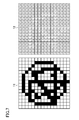
- FIG. 8 is a diagram showing an example output of a display unit of FIG. 1 in the state of FIG. 7 .
- FIG. 9 is a diagram showing how mask information is used where a flag in the image drawing/displaying device of FIG. 1 is “1.”
- FIG. 10 is a diagram showing how the mask information is used where the flag in the image drawing/displaying device of FIG. 1 is “0.”
- FIG. 11 is a block diagram showing a configuration of an image drawing/displaying device according to a second embodiment of the present disclosure.
- FIG. 12 is a diagram showing example states of the image memory and the flag memory of an image drawing/displaying device according to a third embodiment of the present disclosure.
- FIG. 1 is a block diagram showing a configuration of an image drawing/displaying device according to a first embodiment of the present disclosure.
- the image drawing/displaying device of FIG. 1 includes an image memory 11 , a flag memory 12 , an initialization unit 13 , a drawing unit 14 , a non-initialization unit 15 , a flag determination unit 16 , an initial pixel value storage unit 17 , a display unit 18 , a mask information storage unit 19 , and a pixel value reading unit 20 .
- the image memory 11 is configured to store an image to be displayed.
- the flag memory 12 is configured to store, as a 1-bit flag, information indicating whether or not a corresponding pixel in a screen is in the initial state.
- the initialization unit 13 is configured to change the values of all flags in the flag memory 12 to “0” which indicates that a pixel is in the initial state, before beginning to perform a process on one screen of data.
- the drawing unit 14 is configured to write image data of a graphic etc. to the image memory 11 via the non-initialization unit 15 .
- the non-initialization unit 15 is configured to change the value of the flag of a pixel in the flag memory 12 from “0” (initial state) to “1” which indicates that a pixel in the non-initial state when writing has been performed on the pixel in the image memory 11 .
- the initial pixel value storage unit 17 is configured to store the value of a pixel in the screen in the initial state as an initial pixel value.
- the display unit 18 is configured to read image data from the image memory 11 via the flag determination unit 16 , and display the image data.
- the flag determination unit 16 is configured to, when the display unit 18 reads the value of a pixel from the image memory 11 , read a corresponding flag in the flag memory 12 based on the coordinate values of the pixel to determine whether or not the pixel is in the initial state, and if the flag is still “0” (initial state), supply the initial pixel value from the initial pixel value storage unit 17 to the display unit 18 , and otherwise, i.e., if the flag is “1” (non-initial state), read the pixel value in the image memory 11 and supply the pixel value to the display unit 18 .
- the mask information storage unit 19 and the pixel value reading unit 20 will be described below.
- FIG. 2 is a diagram showing example states before initialization of the image memory 11 and the flag memory 12 of FIG. 1 .
- the screen includes 16 pixels ⁇ 16 pixels.
- the image memory 11 of FIG. 2 indicates that a picture of a face is drawn on white background.
- the flag memory 12 of FIG. 2 indicates that flags corresponding to pixels remaining the white background in the image memory 11 are “0” (initial state) and flags corresponding to pixels constituting the picture are “1” (non-initial state).
- the image memory 11 For each pixel, the image memory 11 stores 32-bit data (RGBA) or 24-bit data (color difference signal YUV) in computer graphics. Compared to the flag memory 12 which stores a 1-bit flag for each pixel, the image memory 11 stores a larger amount of information per pixel.
- RGBA 32-bit data
- YUV color difference signal
- FIG. 3 is a diagram showing example states immediately after initialization of the image memory 11 and the flag memory 12 .
- the initialization unit 13 has changed all flags in the flag memory 12 to “0” (initial state). In contrast to this, even after the flag memory 12 has been initialized, the image memory 11 remains unchanged from the state before the initialization.
- the initial pixel value storage unit 17 stores an initial pixel value received from the outside.
- the drawing unit 14 outputs the coordinate values and pixel values of pixels constituting a graphic to be drawn, to replace the pixel values in the image memory 11 corresponding to the output coordinate values with the output pixel values.
- the non-initialization unit 15 changes flags in the flag memory 12 corresponding to the output coordinate values to “1” (non-initial state).
- FIG. 4 is a diagram showing an example graphic which is to be drawn by the drawing unit 14 of FIG. 1 .
- a triangle which is wider than it is high to be drawn.
- FIG. 5 is a diagram showing example states of the image memory 11 and the flag memory 12 immediately after the graphic of FIG. 4 has been drawn.
- the values of pixels corresponding to the drawing data of FIG. 4 have been changed from those of FIG. 3 .
- the value “1” non-initial state
- FIG. 6 is a diagram showing an example graphic which is to be additionally drawn by the drawing unit 14 of FIG. 1 .
- a triangle which is higher than it is wide is to be drawn.
- FIG. 7 is a diagram showing example states of the image memory 11 and the flag memory 12 immediately after the graphic of FIG. 6 has been drawn.
- the image memory 11 of FIG. 7 the pixel values of a portion corresponding to the drawing data of FIG. 6 have been changed from those of FIG. 5 , and therefore, the past and current graphic images coexist.
- the flag memory 12 the value “1” (non-initial state) has been written to form the shape of the drawing data of FIG. 6 over the data of FIG. 5 .
- FIG. 8 is a diagram showing an example output of the display unit 18 of FIG. 1 in the state of FIG. 7 .
- the flag determination unit 16 checks the states of the flags in the flag memory 12 at the coordinate points corresponding to the image data. If the flag is still “0” (initial state), the flag determination unit 16 transfers the initial pixel value stored in the initial pixel value storage unit 17 to the display unit 18 . If the flag is “1” (non-initial state), the flag determination unit 16 reads the value of a pixel at the corresponding coordinate point from the image memory 11 and transfers the pixel value to the display unit 18 .
- the display unit 18 reads from the image memory 11 only the values of pixels corresponding to flags of “1” (non-initial state) in the flag memory 12 of FIG. 7 , and obtains the initial pixel value from the initial pixel value storage unit 17 for the other pixels, whereby the output image shown in FIG. 8 is obtained.
- the amount of access can be reduced by a factor of 7.9.
- the mask information storage unit 19 of FIG. 1 is configured to store mask information indicating which of a plurality of components of each pixel is forbidden to be initialized.
- FIGS. 9 and 10 are diagrams showing how the mask information is used in the flag determination unit 16 of FIG. 1 .
- FIG. 9 shows a case where the flag is “1” (non-initial state) and
- FIG. 10 indicates a case where the flag is “0” (initial state).
- each pixel value includes four components R, G, B, and A, and 1-bit mask information is assigned to each component.
- the components R, G, and B represent red, green, and blue, respectively, and the component A represents semi-transparency.
- the initial pixel value storage unit 17 stores four initial pixel value components Ri, Gi, Bi, and Ai
- the image memory 11 stores four pixel value components Rf, Gf, Bf, and Af
- the mask information storage unit 19 stores 4-bit mask information 0001.
- the flag determination unit 16 when the display unit 18 reads pixel values from the image memory 11 after drawing has been performed, reads flags in the flag memory 12 corresponding to the pixels in order to determine whether or not each of the pixels is in the initial state, and if the corresponding flag is “1” (non-initial state) as shown in FIG. 9 , the pixel value components Rf, Gf, and Bf are supplied from the image memory 11 to the display unit 18 , and if the corresponding flag is “0” (initial state) as shown in FIG. 10 , the initial pixel value components Ri, Gi, and Bi are supplied from the initial pixel value storage unit 17 to the display unit 18 .
- the pixel value component Af is supplied from the image memory 11 to the display unit 18 without using the initial pixel value component Ai from the initial pixel value storage unit 17 .
- operation can be performed in accordance with an application program interface (API) for clearing using a mask.
- API application program interface
- the clearing using a mask is, for example, to clear (or not clear) only the component A of the components R, G, B, and A of a pixel.
- a semi-transparent pattern may always be stored, and may be superimposed on another image.
- the pixel value reading unit 20 When the drawing unit 14 reads a pixel value from the image memory 11 in order to mix a pixel for execution of semi-transparent drawing, the pixel value reading unit 20 reads a flag in the flag memory 12 corresponding to the pixel based on the coordinate values of the pixel to be read in order to determine whether or not the pixel is in the initial state, and if the flag is still “0” (initial state), supplies the initial pixel value from the initial pixel value storage unit 17 to the drawing unit 14 , and otherwise, i.e., if the flag is “1” (non-initial state), reads the pixel value from the image memory 11 and supplies the pixel value to the drawing unit 14 .
- the drawing unit 14 mixes a value supplied from the pixel value reading unit 20 with a pixel value to be drawn at a predetermined ratio, and writes the resultant pixel value to the image memory 11 via the non-initialization unit 15 .
- the non-initialization unit 15 changes the flag of the pixel in the flag memory 12 from “0” (initial state) to “1” (non-initial state).
- the flag memory 12 is an internal memory in an LSI device, external memory access can be further reduced.
- the frequency of IO operation of an LSI device, which has high power consumption, can be reduced.
- FIG. 11 is a block diagram showing a configuration of an image drawing/displaying device according to a second embodiment of the present disclosure.
- the same parts as those of FIG. 1 are indicated by the same reference characters and will not be described.
- the image drawing/displaying device of FIG. 11 includes an unwritten pixel initialization unit 21 instead of the flag determination unit 16 .
- the unwritten pixel initialization unit 21 rewrites pixels in the initial state with an initial pixel value stored in the initial pixel value storage unit 17 based on the flags of the pixels in the flag memory 12 .
- the same operation as that of the first embodiment is performed until the end of drawing by the drawing unit 14 .
- the image memory 11 and the flag memory 12 are in the states shown in FIG. 7 .
- the unwritten pixel initialization unit 21 sequentially checks the values of the flags in the flag memory 12 , and if a flag is still “0” (initial state), rewrites a pixel in the image memory 11 corresponding to that flag with the initial pixel value stored in the initial pixel value storage unit 17 .
- the image memory 11 is in the same state as that of the image output to the display unit 18 of FIG. 8 . Thereafter, the display unit 18 can display the image of FIG. 8 by reading it from the image memory 11 .
- the mask information storage unit 19 stores mask information indicating which of a plurality of components of each pixel is forbidden to be initialized.
- the mask information is used in the unwritten pixel initialization unit 21 as follows. Specifically, for a component for which the mask information indicates initialization permission “0,” as described above, the unwritten pixel initialization unit 21 sequentially checks the values of the flags in the flag memory 12 , and if a flag is still “0” (initial state), rewrites a pixel in the image memory 11 corresponding to that flag with the initial pixel value component stored in the initial pixel value storage unit 17 .
- the pixel value component in the image memory 11 remains unchanged from the previous state no matter whether the flag is “1” (non-initial state) or “0” (initial state).
- the flag determination unit 16 of the first embodiment is not required.
- the display unit 18 is a separate unit. Therefore, when the configuration of the second embodiment is employed, the display unit 18 which is the same as a conventional one can be used, and at the same time, when an image is read from a CPU etc. after drawing has been completed, the same data as that is obtained when the image drawing/displaying device of this embodiment is not used can be obtained, which is convenient.
- FIG. 12 is a diagram showing example states of the image memory 11 and the flag memory 12 of an image drawing/displaying device according to a third embodiment of the present disclosure.
- the device has a configuration similar to that of FIG. 1 , for example. Note that this embodiment can be implemented using the configuration of FIG. 11 .
- this embodiment is different from the first embodiment in that four pixels constituting a block of two pixels (height) ⁇ two pixels (width) in the image memory 11 are managed using one flag in the flag memory 12 .
- the non-initialization unit 15 reads a flag corresponding to the block including the pixel from the flag memory 12 , and if the flag is “0” (initial state), changes the flag to “1” (non-initial state), and writes the desired pixel value to the image memory 11 on a pixel-by-pixel basis, and rewrites the other pixels in the block including that pixel with the initial pixel value stored in the initial pixel value storage unit 17 .
- the flag determination unit 16 checks the values of the flags in the flag memory 12 on a block-by-block basis, if a flag is still “0” (initial state), transfers the initial pixel value stored in the initial pixel value storage unit 17 to the display unit 18 for the corresponding four pixels, and if a flag is “1” (non-initial state), reads the pixel values of the four pixels in the corresponding block from the image memory 11 and transfers the pixel values to the display unit 18 .
- the mask information storage unit 19 stores mask information indicating which of a plurality of components of each pixel is forbidden to be initialized. For a component for which the mask information indicates initialization forbiddance “1,” the non-initialization unit 15 keeps the pixel value component in the image memory 11 unchanged from the previous state no matter whether the flag of the block indicates the non-initial state “1” or the initial state “0.”
- each block includes four pixels, each block may include a larger number of pixels. If the number of pixels in each block is set to be equal to the number of pixels in each block which is the unit of memory access, the compatibility with memory access is increased.
- the image drawing/displaying device of the present disclosure which includes a flag memory for determining the drawing state of each pixel, is useful as memory access reduction means in applications which require memory initialization at the beginning in addition to computer graphics.
Landscapes
- Engineering & Computer Science (AREA)
- Theoretical Computer Science (AREA)
- Physics & Mathematics (AREA)
- General Physics & Mathematics (AREA)
- Computer Hardware Design (AREA)
- General Engineering & Computer Science (AREA)
- Multimedia (AREA)
- Human Computer Interaction (AREA)
- Controls And Circuits For Display Device (AREA)
Abstract
Description
Claims (12)
Applications Claiming Priority (3)
| Application Number | Priority Date | Filing Date | Title |
|---|---|---|---|
| JP2012-015345 | 2012-01-27 | ||
| JP2012015345 | 2012-01-27 | ||
| PCT/JP2012/007956 WO2013111235A1 (en) | 2012-01-27 | 2012-12-12 | Image drawing display device |
Related Parent Applications (1)
| Application Number | Title | Priority Date | Filing Date |
|---|---|---|---|
| PCT/JP2012/007956 Continuation WO2013111235A1 (en) | 2012-01-27 | 2012-12-12 | Image drawing display device |
Publications (2)
| Publication Number | Publication Date |
|---|---|
| US20140292791A1 US20140292791A1 (en) | 2014-10-02 |
| US9711107B2 true US9711107B2 (en) | 2017-07-18 |
Family
ID=48873013
Family Applications (1)
| Application Number | Title | Priority Date | Filing Date |
|---|---|---|---|
| US14/303,453 Expired - Fee Related US9711107B2 (en) | 2012-01-27 | 2014-06-12 | Image drawing/displaying device |
Country Status (2)
| Country | Link |
|---|---|
| US (1) | US9711107B2 (en) |
| WO (1) | WO2013111235A1 (en) |
Citations (8)
| Publication number | Priority date | Publication date | Assignee | Title |
|---|---|---|---|---|
| JPS6122391A (en) | 1984-06-06 | 1986-01-30 | 富士通株式会社 | Copy control system for display |
| JPH02217893A (en) | 1989-02-18 | 1990-08-30 | Fujitsu Ltd | Projection type liquid crystal display device |
| JPH0683297A (en) | 1992-09-03 | 1994-03-25 | Ricoh Co Ltd | Display control device and its display control method |
| JP2003288067A (en) | 2002-03-28 | 2003-10-10 | Hitachi Ltd | Image display device |
| JP2004166017A (en) | 2002-11-14 | 2004-06-10 | Hitachi Ltd | Image display device |
| JP2006276269A (en) | 2005-03-28 | 2006-10-12 | Canon Inc | Image display device, image display method and program thereof |
| US20110018886A1 (en) * | 2007-12-18 | 2011-01-27 | Thales | Display device and method for optimizing the memory bandwith |
| US20130162681A1 (en) * | 2002-05-30 | 2013-06-27 | Adobe Systems Incorporated | Distortion of raster and vector artwork |
-
2012
- 2012-12-12 WO PCT/JP2012/007956 patent/WO2013111235A1/en not_active Ceased
-
2014
- 2014-06-12 US US14/303,453 patent/US9711107B2/en not_active Expired - Fee Related
Patent Citations (9)
| Publication number | Priority date | Publication date | Assignee | Title |
|---|---|---|---|---|
| JPS6122391A (en) | 1984-06-06 | 1986-01-30 | 富士通株式会社 | Copy control system for display |
| JPH02217893A (en) | 1989-02-18 | 1990-08-30 | Fujitsu Ltd | Projection type liquid crystal display device |
| JPH0683297A (en) | 1992-09-03 | 1994-03-25 | Ricoh Co Ltd | Display control device and its display control method |
| US5574483A (en) | 1992-09-03 | 1996-11-12 | Ricoh Company, Ltd. | Display control unit and display control method thereof |
| JP2003288067A (en) | 2002-03-28 | 2003-10-10 | Hitachi Ltd | Image display device |
| US20130162681A1 (en) * | 2002-05-30 | 2013-06-27 | Adobe Systems Incorporated | Distortion of raster and vector artwork |
| JP2004166017A (en) | 2002-11-14 | 2004-06-10 | Hitachi Ltd | Image display device |
| JP2006276269A (en) | 2005-03-28 | 2006-10-12 | Canon Inc | Image display device, image display method and program thereof |
| US20110018886A1 (en) * | 2007-12-18 | 2011-01-27 | Thales | Display device and method for optimizing the memory bandwith |
Non-Patent Citations (1)
| Title |
|---|
| International Search Report issued in International Application No. PCT/JP2012/007956 with Date of mailing Mar. 19, 2013, with English Translation. |
Also Published As
| Publication number | Publication date |
|---|---|
| US20140292791A1 (en) | 2014-10-02 |
| WO2013111235A1 (en) | 2013-08-01 |
Similar Documents
| Publication | Publication Date | Title |
|---|---|---|
| RU2661763C2 (en) | Exploiting frame to frame coherency in architecture of image construction with primitives sorting at intermediate stage | |
| JP5763195B2 (en) | Pixel rendering on the display | |
| EP2245598B1 (en) | Multi-buffer support for off-screen surfaces in a graphics processing system | |
| US8760459B2 (en) | Display data management techniques | |
| CN109166159A (en) | Obtain the method, apparatus and terminal of the dominant hue of image | |
| CN112740278B (en) | Method and apparatus for graphics processing | |
| US9336561B2 (en) | Color buffer caching | |
| CN105190701A (en) | Primitive-based composition | |
| KR20170058113A (en) | Graphic processing apparatus and method for performing graphics pipeline thereof | |
| US11748911B2 (en) | Shader function based pixel count determination | |
| US9424814B2 (en) | Buffer display techniques | |
| US9711107B2 (en) | Image drawing/displaying device | |
| US20110307643A1 (en) | Memory Management Process and Apparatus for the Same | |
| CN109214977B (en) | Image processing device and control method thereof | |
| US20180288353A1 (en) | Low power video composition using a stream out buffer | |
| CN103809972B (en) | A kind of information processing method and electronic equipment | |
| US12412495B2 (en) | Image processing device, operating method thereof, and display system including image processing device | |
| US20090219299A1 (en) | Method and system for dynamic color allocation for anti-aliased images in palette-based systems | |
| WO2024187862A1 (en) | Image processing method, apparatus, computer device, and storage medium | |
| KR20230053597A (en) | image-space function transfer | |
| CN113313800A (en) | Texture-based pixel count determination |
Legal Events
| Date | Code | Title | Description |
|---|---|---|---|
| AS | Assignment |
Owner name: PANASONIC CORPORATION, JAPAN Free format text: ASSIGNMENT OF ASSIGNORS INTEREST;ASSIGNOR:WAKAYAMA, YORIHIKO;REEL/FRAME:033481/0178 Effective date: 20140523 |
|
| AS | Assignment |
Owner name: PANASONIC INTELLECTUAL PROPERTY MANAGEMENT CO., LTD., JAPAN Free format text: ASSIGNMENT OF ASSIGNORS INTEREST;ASSIGNOR:PANASONIC CORPORATION;REEL/FRAME:034194/0143 Effective date: 20141110 Owner name: PANASONIC INTELLECTUAL PROPERTY MANAGEMENT CO., LT Free format text: ASSIGNMENT OF ASSIGNORS INTEREST;ASSIGNOR:PANASONIC CORPORATION;REEL/FRAME:034194/0143 Effective date: 20141110 |
|
| STCF | Information on status: patent grant |
Free format text: PATENTED CASE |
|
| AS | Assignment |
Owner name: PANASONIC INTELLECTUAL PROPERTY MANAGEMENT CO., LTD., JAPAN Free format text: CORRECTIVE ASSIGNMENT TO CORRECT THE ERRONEOUSLY FILED APPLICATION NUMBERS 13/384239, 13/498734, 14/116681 AND 14/301144 PREVIOUSLY RECORDED ON REEL 034194 FRAME 0143. ASSIGNOR(S) HEREBY CONFIRMS THE ASSIGNMENT;ASSIGNOR:PANASONIC CORPORATION;REEL/FRAME:056788/0362 Effective date: 20141110 |
|
| FEPP | Fee payment procedure |
Free format text: MAINTENANCE FEE REMINDER MAILED (ORIGINAL EVENT CODE: REM.); ENTITY STATUS OF PATENT OWNER: LARGE ENTITY |
|
| LAPS | Lapse for failure to pay maintenance fees |
Free format text: PATENT EXPIRED FOR FAILURE TO PAY MAINTENANCE FEES (ORIGINAL EVENT CODE: EXP.); ENTITY STATUS OF PATENT OWNER: LARGE ENTITY |
|
| STCH | Information on status: patent discontinuation |
Free format text: PATENT EXPIRED DUE TO NONPAYMENT OF MAINTENANCE FEES UNDER 37 CFR 1.362 |
|
| FP | Lapsed due to failure to pay maintenance fee |
Effective date: 20210718 |