US9704642B2 - Information transmission apparatus and system using inductive coupling between coils - Google Patents
Information transmission apparatus and system using inductive coupling between coils Download PDFInfo
- Publication number
- US9704642B2 US9704642B2 US13/983,664 US201213983664A US9704642B2 US 9704642 B2 US9704642 B2 US 9704642B2 US 201213983664 A US201213983664 A US 201213983664A US 9704642 B2 US9704642 B2 US 9704642B2
- Authority
- US
- United States
- Prior art keywords
- coil
- transmitter
- receiver
- receiver coil
- plane
- Prior art date
- Legal status (The legal status is an assumption and is not a legal conclusion. Google has not performed a legal analysis and makes no representation as to the accuracy of the status listed.)
- Expired - Fee Related, expires
Links
Images


Classifications
-
- H—ELECTRICITY
- H01—ELECTRIC ELEMENTS
- H01F—MAGNETS; INDUCTANCES; TRANSFORMERS; SELECTION OF MATERIALS FOR THEIR MAGNETIC PROPERTIES
- H01F38/00—Adaptations of transformers or inductances for specific applications or functions
- H01F38/14—Inductive couplings
-
- H—ELECTRICITY
- H01—ELECTRIC ELEMENTS
- H01F—MAGNETS; INDUCTANCES; TRANSFORMERS; SELECTION OF MATERIALS FOR THEIR MAGNETIC PROPERTIES
- H01F27/00—Details of transformers or inductances, in general
- H01F27/28—Coils; Windings; Conductive connections
- H01F27/2871—Pancake coils
-
- H02J17/00—
-
- H—ELECTRICITY
- H02—GENERATION; CONVERSION OR DISTRIBUTION OF ELECTRIC POWER
- H02J—CIRCUIT ARRANGEMENTS OR SYSTEMS FOR SUPPLYING OR DISTRIBUTING ELECTRIC POWER; SYSTEMS FOR STORING ELECTRIC ENERGY
- H02J50/00—Circuit arrangements or systems for wireless supply or distribution of electric power
- H02J50/10—Circuit arrangements or systems for wireless supply or distribution of electric power using inductive coupling
- H02J50/12—Circuit arrangements or systems for wireless supply or distribution of electric power using inductive coupling of the resonant type
-
- H—ELECTRICITY
- H02—GENERATION; CONVERSION OR DISTRIBUTION OF ELECTRIC POWER
- H02J—CIRCUIT ARRANGEMENTS OR SYSTEMS FOR SUPPLYING OR DISTRIBUTING ELECTRIC POWER; SYSTEMS FOR STORING ELECTRIC ENERGY
- H02J50/00—Circuit arrangements or systems for wireless supply or distribution of electric power
- H02J50/70—Circuit arrangements or systems for wireless supply or distribution of electric power involving the reduction of electric, magnetic or electromagnetic leakage fields
-
- H—ELECTRICITY
- H02—GENERATION; CONVERSION OR DISTRIBUTION OF ELECTRIC POWER
- H02J—CIRCUIT ARRANGEMENTS OR SYSTEMS FOR SUPPLYING OR DISTRIBUTING ELECTRIC POWER; SYSTEMS FOR STORING ELECTRIC ENERGY
- H02J50/00—Circuit arrangements or systems for wireless supply or distribution of electric power
- H02J50/80—Circuit arrangements or systems for wireless supply or distribution of electric power involving the exchange of data, concerning supply or distribution of electric power, between transmitting devices and receiving devices
-
- H04B5/0031—
-
- H04B5/0037—
-
- H04B5/0093—
-
- H—ELECTRICITY
- H04—ELECTRIC COMMUNICATION TECHNIQUE
- H04B—TRANSMISSION
- H04B5/00—Near-field transmission systems, e.g. inductive or capacitive transmission systems
- H04B5/20—Near-field transmission systems, e.g. inductive or capacitive transmission systems characterised by the transmission technique; characterised by the transmission medium
- H04B5/24—Inductive coupling
- H04B5/26—Inductive coupling using coils
- H04B5/266—One coil at each side, e.g. with primary and secondary coils
-
- H—ELECTRICITY
- H04—ELECTRIC COMMUNICATION TECHNIQUE
- H04B—TRANSMISSION
- H04B5/00—Near-field transmission systems, e.g. inductive or capacitive transmission systems
- H04B5/70—Near-field transmission systems, e.g. inductive or capacitive transmission systems specially adapted for specific purposes
- H04B5/79—Near-field transmission systems, e.g. inductive or capacitive transmission systems specially adapted for specific purposes for data transfer in combination with power transfer
-
- H—ELECTRICITY
- H05—ELECTRIC TECHNIQUES NOT OTHERWISE PROVIDED FOR
- H05B—ELECTRIC HEATING; ELECTRIC LIGHT SOURCES NOT OTHERWISE PROVIDED FOR; CIRCUIT ARRANGEMENTS FOR ELECTRIC LIGHT SOURCES, IN GENERAL
- H05B6/00—Heating by electric, magnetic or electromagnetic fields
- H05B6/02—Induction heating
- H05B6/10—Induction heating apparatus, other than furnaces, for specific applications
- H05B6/12—Cooking devices
- H05B6/1209—Cooking devices induction cooking plates or the like and devices to be used in combination with them
- H05B6/1236—Cooking devices induction cooking plates or the like and devices to be used in combination with them adapted to induce current in a coil to supply power to a device and electrical heating devices powered in this way
-
- H02J5/005—
-
- H—ELECTRICITY
- H05—ELECTRIC TECHNIQUES NOT OTHERWISE PROVIDED FOR
- H05B—ELECTRIC HEATING; ELECTRIC LIGHT SOURCES NOT OTHERWISE PROVIDED FOR; CIRCUIT ARRANGEMENTS FOR ELECTRIC LIGHT SOURCES, IN GENERAL
- H05B2213/00—Aspects relating both to resistive heating and to induction heating, covered by H05B3/00 and H05B6/00
- H05B2213/06—Cook-top or cookware capable of communicating with each other
-
- Y—GENERAL TAGGING OF NEW TECHNOLOGICAL DEVELOPMENTS; GENERAL TAGGING OF CROSS-SECTIONAL TECHNOLOGIES SPANNING OVER SEVERAL SECTIONS OF THE IPC; TECHNICAL SUBJECTS COVERED BY FORMER USPC CROSS-REFERENCE ART COLLECTIONS [XRACs] AND DIGESTS
- Y02—TECHNOLOGIES OR APPLICATIONS FOR MITIGATION OR ADAPTATION AGAINST CLIMATE CHANGE
- Y02B—CLIMATE CHANGE MITIGATION TECHNOLOGIES RELATED TO BUILDINGS, e.g. HOUSING, HOUSE APPLIANCES OR RELATED END-USER APPLICATIONS
- Y02B40/00—Technologies aiming at improving the efficiency of home appliances, e.g. induction cooking or efficient technologies for refrigerators, freezers or dish washers
-
- Y02B40/123—
Definitions
- the present disclosure relates to a noncontact connector apparatus and a noncontact connector system, each using inductive coupling between coils, and an information transmission apparatus and an information transmission system including the same apparatus and system.
- the noncontact power feeding apparatus of the Patent Document 1 is characterized by including a furniture with a power primary coil supplied with electric power, a cordless device including a power secondary coil arranged in magnetic fluxes caused by the power primary coil in such a state that the same apparatus is arranged in a predetermined arrangement position with respect to the furniture, and informing means for informing of the predetermined arrangement position of the cordless device with respect to the furniture.
- the contactless power transfer coil of the Patent Document 2 is characterized by including a planar coil formed by winding a linear conductor in a spiral form within a roughly identical plane, and a magnetic layer that is formed by coating a liquid magnetic material solution in which magnetic particles are mixed in a binder solvent and coated so as to cover one planar portion of the planar coil and a side surface portion of the planar coil.
- the wireless transmission system of the Patent Document 3 includes a resonator for wireless power transfer, and this has a conductor that forms one or more loops and has a predetermined inductance, and a capacitor network that has predetermined capacitances and desired electrical parameters and is connected to the conductor.
- the capacitor network includes at least one capacitor of a first type having a first temperature profile as an electrical parameter, and at least one capacitor of a second type having a second temperature profile as an electrical parameter.
- noncontact power transfer system The principle of such a noncontact power transfer system is applicable also to an information transmission system including a noncontact connector apparatus and an induction heating apparatus such as an IH cooking apparatus and the like.
- Patent Document 1 Japanese patent laid-open publication No. JP 2001-309579 A;
- Patent Document 2 Japanese patent laid-open publication No. JP 2008-172873 A;
- Patent Document 3 U.S. patent application publication No. US 2010/0181845 A1.
- a transmitter coil provided for the power transfer apparatus e.g., charger
- a receiver coil provided for the power transfer apparatus e.g., object to be charged
- An object of the present disclosure is to provide an information transmission apparatus and an information transmission system that are tolerant of positional misalignment of the transmitter coil and the receiver coil and has a high transmission efficiency with a simple configuration.
- an information transmission apparatus including a transmitter circuit configured to transmit information to a receiver circuit connected to a receiver coil; and a first noncontact connector apparatus connected to the transmitter circuit.
- the first noncontact connector apparatus comprises a transmitter coil, that is provided to be adjacent so as to be electromagnetically coupled to the receiver coil, and a winding of the transmitter coil is wound on a first plane.
- the information transmission apparatus includes a first magnetic body provided between the first plane and a second plane which is opposed to be adjacent to the first plane and on which the receiver coil is provided, and the first magnetic body is provided to be adjacent so as to be electromagnetically coupled to the transmitter coil and to cover at least one part of a region in which at least the winding of the transmitter coil exists.
- an information transmission apparatus including: a receiver circuit configured to receive information from a transmitter circuit connected to a transmitter coil; and a second noncontact connector apparatus connected to the receiver circuit.
- the second noncontact connector apparatus includes a receiver coil, that is provided to be adjacent so as to be electromagnetically coupled to the transmitter coil, and a winding of the receiver coil is wound on a second plane that is opposed to be adjacent to the first plane on which the transmitter coil is provided.
- the information transmission apparatus includes a second magnetic body provided between the first plane and the second plane, and the second magnetic body is provided to be adjacent so as to be electromagnetically coupled to the receiver coil and to cover at least one part of a region in which at least the winding of the receiver coil exists.
- an information transmission system including: the information transmission apparatus according to the first or second aspect of the present disclosure serving as a first information transmission apparatus including the transmitter circuit; and a second information transmission apparatus including the receiver circuit, and a second noncontact connector apparatus connected to the receiver circuit.
- the second noncontact connector apparatus comprises a receiver coil including a winding wound on the second plane.
- the first magnetic body is further put to be adjacent to the receiver coil to be electromagnetically coupled to the receiver coil and to cover at least one part of a region in which at least the winding of the receiver coil exists between the first plane and the second plane, thereby increasing the self-inductance of the receiver coil by putting the first magnetic body to be adjacent to the receiver coil.
- a coupling coefficient between the transmitter coil and the receiver coil is set to be decreased by increasing the self-inductance of each of the transmitter coil and the receiver coil so that a frequency characteristic of transmission efficiency from the transmitter coil to the receiver coil changes from a double-peaked narrow-band characteristic to a single-peaked wide-band characteristic.
- an information transmission system including: the information transmission apparatus according the first or second aspect of the present disclosure serving as a first information transmission apparatus including the transmitter circuit; and the information transmission apparatus according to the third or fourth aspect of the present disclosure serving as a second information transmission apparatus including the receiver circuit.
- a coupling coefficient between the transmitter coil and the receiver coil is set to be decreased by increasing the self-inductance of each of the transmitter coil and the receiver coil so that a frequency characteristic of transmission efficiency from the transmitter coil to the receiver coil changes from a double-peaked narrow-band characteristic to a single-peaked wide-band characteristic.
- information can be transmitted with a stabilized transmission efficiency with a very simple configuration even if positional misalignment occurs between the transmitter coil and the receiver coil.
- FIG. 1 is a perspective view showing a schematic configuration of a power transfer system according to a first embodiment of the present disclosure
- FIG. 2 is a sectional view along a line A-A′ of FIG. 1 ;
- FIG. 3 is a sectional view showing a schematic configuration of a power transfer system of a comparative example
- FIG. 4 is a circuit diagram showing one example of an equivalent circuit of the power transfer system of FIG. 3 ;
- FIG. 5 is a schematic diagram showing frequency characteristics of transmission efficiency when a coupling coefficient k between a transmitter coil 1 and a receiver coil 2 of FIG. 3 is changed;
- FIG. 6 is a schematic diagram showing flows of magnetic fluxes in the power transfer system of FIG. 3 ;
- FIG. 7 is a schematic diagram showing flows of magnetic fluxes when a distance d between the transmitter coil 1 and the receiver coil 2 is increased in the power transfer system of FIG. 3 ;
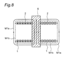
- FIG. 8 is a schematic diagram showing flows of magnetic fluxes when the distance “d” between the transmitter coil 1 and the receiver coil 2 is increased and a magnetic material 6 is inserted in the power transfer system of FIG. 3 ;
- FIG. 9 is a schematic diagram showing flows of magnetic fluxes in the power transfer system of FIG. 1 ;
- FIG. 10 is a schematic diagram showing flows of magnetic fluxes when the transmitter coil 1 and the receiver coil 2 are misaligned in position in the power transfer system of FIG. 1 ;
- FIG. 11 is a perspective view showing a schematic configuration of a power transfer system according to a first implemental example of the present disclosure
- FIG. 12 is a top view of the power transfer system of FIG. 11 ;
- FIG. 13 is a sectional view along a line B-B′ of FIG. 11 ;
- FIG. 14 is a circuit diagram showing an equivalent circuit of the power transfer system of FIG. 11 ;
- FIG. 15 is a diagram showing a positional misalignment generated between the transmitter coil 1 and the receiver coil 2 in the power transfer system of FIG. 11 ;
- FIG. 16 is a graph showing frequency characteristics of transmission efficiency when the positional misalignment of the transmitter coil 1 and the receiver coil 2 is changed in the power transfer system of FIG. 11 from which the magnetic material 3 is removed;
- FIG. 17 is a graph showing frequency characteristics of transmission efficiency when the positional misalignment of the transmitter coil 1 and the receiver coil 2 is changed in the power transfer system of FIG. 11 ;
- FIG. 18 is a graph showing characteristics of transmission efficiency with respect to the positional misalignment of the power transfer system of FIG. 11 ;
- FIG. 19 is a graph showing frequency characteristics of transmission efficiency when a relative permeability of the magnetic material 3 is changed in the power transfer system of FIG. 11 ;
- FIG. 20 is a graph showing frequency characteristics of transmission efficiency when the relative permeability of the magnetic material 3 is changed in the power transfer system of FIG. 11 in which the thickness of the magnetic material 3 is reduced;
- FIG. 21 is a graph showing frequency characteristics of transmission efficiency when the relative permeability of the magnetic material 3 is changed in the power transfer system of FIG. 11 in which the thickness of the magnetic material 3 is reduced;
- FIG. 22 is a top view showing a schematic configuration of a power transfer system according to a second implemental example of the present disclosure
- FIG. 23 is a graph showing frequency characteristics of transmission efficiency when the relative permeability of the magnetic material 3 is changed in the power transfer system of FIG. 22 from which a cavity is removed;
- FIG. 24 is a graph showing frequency characteristics of transmission efficiency when the relative permeability of the magnetic material 3 is changed in the power transfer system of FIG. 22 ;
- FIG. 25 is a sectional view showing a schematic configuration of a power transfer system according to a third implemental example of the present disclosure.
- FIG. 26 is a plan view showing a transmitter coil 1 and a receiver coil 2 of FIG. 25 ;
- FIG. 27 is a graph showing frequency characteristics of transmission efficiency of the power transfer system of FIG. 25 ;
- FIG. 28 is a block diagram showing a schematic configuration of the power transfer system of the first embodiment of the present disclosure.
- FIG. 29 is a sectional view showing a configuration of a power transfer apparatus on the power transmitter side and a power transfer apparatus on the power receiver side in the power transfer system of FIG. 25 ;
- FIG. 30 is a sectional view showing a configuration of a modified embodiment of the power transfer apparatus on the power transmitter side and the power transfer apparatus on the power receiver side in the power transfer system of FIG. 25 ;
- FIG. 31 is a block diagram showing a schematic configuration of a signal transmission system according to a second embodiment of the present disclosure.
- FIG. 32 is a block diagram showing a schematic configuration of an induction heating apparatus according to a third embodiment of the present disclosure.
- FIG. 33 is a sectional view showing a configuration of the induction heating apparatus and the pan 123 of FIG. 32 ;
- FIG. 34 is a sectional view showing a modified embodiment of the transmitter coil 1 and the receiver coil 2 of FIG. 1 ;
- FIG. 35 is a schematic diagram for explaining a winding method of the transmitter coil 1 of FIG. 34 ;
- FIG. 36 is a schematic diagram for explaining a modified embodiment of the winding method of the transmitter coil 1 of FIG. 34 ;
- FIG. 37 is a sectional view showing a modified embodiment of the noncontact connector apparatuses on the transmitter side and the power receiver side of FIG. 1 ;
- FIG. 38 is a perspective view showing a schematic configuration of a power transfer system according to a fourth embodiment of the present disclosure.
- FIG. 39 is a perspective view showing a schematic configuration of a power transfer system according to a fifth embodiment of the present disclosure.
- FIG. 40 is a vertical sectional view showing a schematic configuration of a power transfer system according to a fourth implemental example of the present disclosure.
- FIG. 41 is a graph showing characteristics of the coupling coefficient k with respect to a permeability ratio ⁇ 2/ ⁇ 1 when a normalized inter-coil distance d/D is used as a parameter in the power transfer system of FIG. 40 .
- FIG. 1 is a perspective view showing a schematic configuration of a power transfer system according to the first embodiment of the present disclosure.
- FIG. 2 is a sectional view along a line A-A′ of FIG. 1 .
- the power transfer system of the present embodiment is configured to include a noncontact connector system that uses electromagnetical coupling between a transmitter coil 1 and a receiver coil 2 .
- a power supply, a power transmitter circuit, a power receiver circuit and so on which is beneficial for use in a power transfer system are omitted for simplicity of illustration, and only the noncontact connector system is shown.
- the noncontact connector system is assumed to be configured to include a noncontact connector apparatus that includes a transmitter coil 1 on the transmitter side, and a noncontact connector apparatus that includes a receiver coil 2 on the receiver side.
- the noncontact connector system is configured to include the transmitter coil 1 and the receiver coil 2 , which are provided along a first plane and a second plane, respectively, and arranged to be adjacent and oppose to each other.
- the transmitter coil 1 has terminals P 1 a and P 1 b
- the receiver coil 2 has terminals P 2 a and P 2 b .
- the transmitter coil 1 and the receiver coil 2 are arranged to be adjacent to each other so as to be electromagnetically coupled to each other.
- the transmitter coil 1 is provided along the first plane so that its winding is wound around the peripheries of a predetermined region on the first plane.
- the receiver coil 2 is provided along the second plane so that its winding is wound around the peripheries of a predetermined region on the second plane.
- the noncontact connector system is configured to include a magnetic material 3 having a predetermined relative permeability.
- the magnetic material 3 is provided between the first and second planes, so as to be electromagnetically coupled to the transmitter coil 1 and the receiver coil 2 and to cover at least one part of a region, in which the windings of the transmitter coil 1 and the receiver coil 2 exist between the first plane and the second plane.
- the magnetic material 3 is made of, for example, ferrite.
- a self-inductance of the transmitter coil 1 is increased by putting the magnetic material 3 to be adjacent to the magnetic material 3
- a self-inductance of the receiver coil 2 is increased by putting the magnetic material 3 to be adjacent to the receiver coil 2 .
- the power transfer system of the present embodiment is characterized in that a coupling coefficient between the transmitter coil 1 and the receiver coil 2 is set to be decreased by increasing the self-inductances of the transmitter coil 1 and the receiver coil 2 , so that a frequency characteristic of transmission efficiency from the transmitter coil 1 to the receiver coil 2 changes from a double-peaked narrow-band characteristic to a single-peaked wide-band characteristic.
- FIG. 3 is a sectional view showing a schematic configuration of the power transfer system of a comparative example.
- the noncontact connector system is similar to the noncontact connector system of FIG. 1 except for not having the magnetic material 3 .
- the transmitter coil 1 is provided in a casing 4 of the noncontact connector apparatus on the transmitter side
- the receiver coil 2 is provided in a casing 5 of the noncontact connector apparatus on the receiver side.
- the transmitter coil 1 and the receiver coil 2 are separated to be apart by a distance d provided therebetween.
- L 1 represents the self-inductance of the transmitter coil 1
- L 2 represents the self-inductance of the receiver coil 2 .
- FIG. 4 is a circuit diagram showing one example of an equivalent circuit of the power transfer system of FIG. 3 .
- Q is a signal source
- z 01 is the load impedance of the transmitter circuit
- z 02 is the load impedance of the receiver circuit and the load.
- R 1 and R 2 are resistors
- C 1 and C 2 are capacitors for impedance matching.
- FIG. 5 is a schematic graph showing frequency characteristics of transmission efficiency when the coupling coefficient k between the transmitter coil 1 and the receiver coil 2 of FIG. 3 is changed.
- the Q value is constant.
- FIG. 5 it can be understood that the bandwidth of transmission efficiency changes in accordance with the magnitude of the coupling coefficient k.
- the coupling coefficient k is a ratio of the square root of the self-inductances L 1 and L 2 to the mutual inductance M, the coupling coefficient k can be decreased if the self-inductances L 1 and L 2 can be increased.
- FIGS. 6 to 8 are schematic diagrams showing flows of magnetic fluxes in the power transfer system of FIG. 3 , respectively.
- the casings 4 and 5 of FIG. 3 are omitted, and the transmitter coil 1 and the receiver coil 2 are only shown.
- magnetic fluxes M 1 a and M 1 b are formed so as to surround both of the transmitter coil 1 and the receiver coil 2 , and the mutual inductance M increases, making the coupling coefficient k higher.
- FIG. 7 is a schematic diagram showing flows of magnetic fluxes when the distance d between the transmitter coil 1 and the receiver coil 2 is increased in the power transfer system of FIG. 3 .
- the transmitter coil 1 and the receiver coil 2 are apart from each other as shown in FIG. 7 .
- magnetic fluxes M 2 a and M 2 b partially become leakage fluxes among the magnetic fluxes formed in the peripheries of the transmitter coil 1 and receiver coil 2 , and therefore, the mutual inductance M decreases, making the coupling coefficient k lower.
- FIG. 8 is a schematic diagram showing flows of the magnetic fluxes when the distance d between the transmitter coil 1 and the receiver coil 2 is increased, and a magnetic material 6 is inserted in the power transfer system of FIG. 3 .
- the magnetic material 6 iron, ferrite, or the like
- the leakage fluxes M 2 a and M 2 b of FIG. 7 can be changed into a magnetic flux M 1 b surrounding both of the transmitter coil 1 and the receiver coil 2 through the inside of the magnetic material 6 , consequently increasing the mutual inductance M and making the coupling coefficient k higher.
- the coupling coefficient k becomes higher as described before, and therefore, any wide band operation cannot be achieved. Therefore, it is beneficial to increase the self-inductances L 1 and L 2 by controlling the flows of the magnetic fluxes instead of decreasing the mutual inductance M.
- FIG. 9 is a schematic diagram showing flows of magnetic fluxes in the power transfer system of FIG. 1 .
- a partial magnetic flux M 1 is formed so as to surround both of the transmitter coil 1 and the receiver coil 2 through the magnetic material 3 .
- the other partial magnetic flux M 2 a is not directed toward the receiver coil 2 passing only in the vicinity of the transmitter coil 1 in the magnetic material 3 and but formed as a leakage flux surrounding only the transmitter coil 1 .
- the leakage flux M 2 a the self-inductance L 1 of the transmitter coil 1 increases.
- the magnetic flux is not directed toward the transmitter coil 1 passing only in the vicinity of the receiver coil 2 in the magnetic material 3 , but forms the leakage flux M 2 b surrounding only the receiver coil 2 .
- the leakage flux M 2 b By forming the leakage flux M 2 b , the self-inductance L 2 of the receiver coil 2 increases.
- the self-inductances L 1 and L 2 increase due to the magnetic material 3 provided, and the coupling coefficient k is decreased by comparison with the case of FIG. 6 , therefore allowing the wide band operation to be achieved.
- FIG. 10 is a schematic diagram showing flows of magnetic fluxes when the transmitter coil 1 and the receiver coil 2 are misaligned in position in the power transfer system of FIG. 1 .
- the leakage flux M 2 a surrounding only the transmitter coil 1 and the leakage flux M 2 b surrounding only the receiver coil 2 are formed in a manner similar to that of the case of FIG. 9 . Therefore, the self-inductances L 1 and L 2 increase due to the magnetic material 3 provided in a manner similar to that of the case of FIG. 9 , and the coupling coefficient k is decreased by comparison with the case of FIG. 6 , and therefore this allows the wide band operation to be achieved.
- the beneficial coupling coefficient k is described with reference to FIG. 5 .
- the coupling coefficient k gradually decreases, a frequency interval between the two peaks of transmission efficiency gradually decreases, and the minimum value of transmission efficiency between the two peaks gradually increases.
- the frequency interval becomes substantially zero, i.e., when a difference between the two peaks of transmission efficiency and the minimum value between them decreases (e.g., 5 to 10%), the bandwidth of the power transfer system is maximized.
- the coupling coefficient k is determined so as to satisfy this beneficial point, and the parameters (the thickness and the relative permeability of the magnetic material 3 , the number of turns of the transmitter coil 1 and the receiver coil 2 , etc.) of the power transfer system are determined so as to achieve this value of the coupling coefficient k.
- the coupling coefficient k decreases due to the effects of the magnetic material 3 , and wide band operation can be achieved in the case of the power transfer system of the present embodiment.
- the resonance frequency decreases from 250 kHz to 150 kHz due to increases in the self-inductances L 1 and L 2 when the magnetic material 3 is provided. In other words, a size reduction effect can also be obtained due to the decrease in the resonance frequency in the power transfer system of the present embodiment.
- FIG. 11 is a perspective view showing a schematic configuration of the power transfer system according to the first implemental example of the present disclosure.
- FIG. 12 is a top view of the power transfer system of FIG. 11 .
- FIG. 13 is a sectional view along a line B-B′ of FIG. 11 .
- the transmitter coil 1 and the receiver coil 2 are rectangular coils that have square outer peripheries of 30 mm ⁇ 30 mm, a wiring width of 0.4 mm, a wiring pitch of 0.4 mm, and a wiring thickness of 0.2 mm, and a number of turns is five.
- FIG. 14 is a circuit diagram showing an equivalent circuit of the power transfer system of FIG. 11 .
- Q 1 is a signal source
- Z 1 is a load impedance
- C 3 and C 4 are capacitors loaded for impedance matching.
- the capacitors C 3 and C 4 have a capacitance of 20 nF.
- FIG. 15 is a diagram for explaining positional misalignments generated between the transmitter coil 1 and the receiver coil 2 in the power transfer system of FIG. 11 .
- the receiver coil 2 was displaced in the Y direction with respect to the transmitter coil 1 as shown in FIG. 15 . It is assumed that the magnetic material 3 has a sufficient length in the Y direction so that the displacement in FIG. 15 can be achieved.
- an impedance matrix between the transmitter coil 1 and the receiver coil 2 was calculated by using the finite element method, and 100 ⁇
- FIG. 16 is a graph showing a frequency characteristic of transmission efficiency when the positional misalignment of the transmitter coil 1 and the receiver coil 2 is changed in the power transfer system of FIG. 11 from which the magnetic material 3 is removed.
- FIG. 17 is a graph showing a frequency characteristic of transmission efficiency when the positional misalignment of the transmitter coil 1 and the receiver coil 2 is changed in the power transfer system of FIG. 11 . It can be understood that the resonance frequency shifts to a higher frequency as the displacement between the transmitter coil 1 and the receiver coil 2 increases, and the transmission efficiency decreases in the absence of the magnetic material 3 ( FIG. 16 ). Assuming that the operating frequency is about 700 kHz, then large fluctuations occur in the transmission efficiency.
- FIG. 18 is a graph showing a characteristic of transmission efficiency with respect to the positional misalignment of the power transfer system of FIG. 11 .
- the configuration of the power transfer system is similar to that shown in FIGS. 11 to 14 , and the operating frequency is 680 kHz.
- the comparative example (with no magnetic material) is tolerant of a displacement of up to 5 mm
- the implemental example is tolerant of a positional misalignment up to 13 mm. It can be understood that the power transfer system of the present embodiment has a great tolerance to the positional misalignment of the transmitter coil 1 and the receiver coil 2 .
- FIGS. 19 to 21 a characteristic when the relative permeability of the magnetic material 3 is changed in the power transfer system of the present embodiment is described with reference to FIGS. 19 to 21 .
- the configuration of the power transfer system is similar to that shown in FIGS. 11 to 14 except for the thickness (equal to the distance between the transmitter coil 1 and the receiver coil 2 ) and the relative permeability of the magnetic material 3 .
- the capacitors C 3 and C 4 have a capacitance of 10 nF.
- FIG. 19 is a graph showing a frequency characteristic of transmission efficiency when the relative permeability of the magnetic material 3 is changed in the power transfer system of FIG. 11 .
- the thickness of the magnetic material 3 is 2 mm.
- FIG. 20 is a graph showing a frequency characteristic of transmission efficiency when the relative permeability of the magnetic material 3 is changed in the power transfer system of FIG. 11 in which the thickness of the magnetic material 3 is reduced.
- the thickness of the magnetic material 3 was 1 mm, and the relative permeability ⁇ r identical to the value in the case of FIG. 19 was used for the sake of comparison.
- the coupling coefficient k between the transmitter coil 1 and the receiver coil 2 increases.
- FIG. 20 is a graph showing a frequency characteristic of transmission efficiency when the relative permeability of the magnetic material 3 is changed in the power transfer system of FIG. 11 in which the thickness of the magnetic material 3 is reduced.
- the thickness of the magnetic material 3 was 1 mm, and the relative permeability ⁇ r identical to the value in the case of FIG. 19 was used for the sake of comparison.
- FIG. 22 is a top view showing a schematic configuration of a power transfer system according to the second implemental example of the present disclosure.
- the power transfer system of FIG. 22 has a configuration similar to that of the power transfer system shown in FIGS. 11 to 14 except that a cavity is provided at the magnetic material 3 .
- the dimensions of the cavity are 14 ⁇ 14 mm.
- FIG. 23 is a graph showing a frequency characteristic of transmission efficiency when the relative permeability of the magnetic material 3 is changed in the power transfer system of FIG. 22 in which the cavity is removed.
- FIG. 24 is a graph showing a frequency characteristic of transmission efficiency when the relative permeability of the magnetic material 3 is changed in the power transfer system of FIG. 22 .
- the magnetic material 3 needs only to be provided adjacent to the transmitter coil 1 and the receiver coil 2 so as to cover at least one part of the region in which at least the windings of the transmitter coil 1 and the receiver coil 2 exist. Providing the cavity at the magnetic material 3 leads to reductions in cost and weight.
- FIG. 25 is a sectional view showing a schematic configuration of a power transfer system according to the third implemental example of the present disclosure.
- FIG. 26 is a plan view showing a transmitter coil 1 and a receiver coil 2 of FIG. 25 .
- a magnetic material 11 and a metal shield 12 are provided for shielding below the transmitter coil 1
- a magnetic material 13 and a metal shield 14 are provided for shielding also above the receiver coil 2 .
- the magnetic materials 11 and 13 and the metal shields 12 and 14 have a thickness of 0.1 mm.
- the shield has the advantageous effects of reducing leakage electromagnetic fields and reducing influences on the peripheral units.
- the magnetic material 3 has a relative permeability of 10, and the magnetic materials 11 and 13 have a relative permeability of 1000. As shown in FIG.
- the transmitter coil 1 and the receiver coil 2 are circular coils that have an outer diameter of 29 mm, an inner diameter of 12.5 mm, and a number of turns of 17.
- the windings of the transmitter coil 1 and the receiver coil 2 have a width of 0.48 mm and a thickness of 0.3 mm, and each of the transmitter coil 1 and the receiver coil 2 has an inductance of 11.7 ⁇ H and a series resistance of 0.4 ⁇ .
- FIG. 27 is a graph showing a frequency characteristic of the transmission efficiency of the power transfer system of FIG. 25 .
- the transmitter coil 1 and the receiver coil 2 are adjacent to be each other so as to be electromagnetically strongly coupled to each other, and therefore, any wide band operation cannot be achieved although the transmission efficiency is maximized at a frequency of 150 kHz.
- the mutual inductance decreases due to the fact that the transmitter coil 1 and the receiver coil 2 are separated to be apart from each other, and therefore, the coupling coefficient can be decreased, consequently allowing the wide band operation to be achieved.
- the frequency at which the transmission efficiency becomes maximized increases to 250 kHz. That is, the power transfer system is substantially increased in size.
- the frequency characteristic of the transmission efficiency of the power transfer system of the implemental example becomes maximized at 150 kHz
- the bandwidth of transmission efficiency e.g., bandwidth in which the transmission efficiency becomes equal to or larger than 60%
- the frequency at which the transmission efficiency becomes maximized is lowered.
- FIG. 28 is a block diagram showing a schematic configuration of the power transfer system according to the first embodiment of the present disclosure.
- a power transfer system including the noncontact connector system as described above can be configured. It is assumed that the power transfer system is configured to include a power transfer apparatus on the power transmitter side on which the noncontact connector apparatus on the transmitter side is provided, and a power transfer apparatus on the power receiver side on which the noncontact connector apparatus on the receiver side is provided.
- the transmitter coil 1 FIG. 1
- the power transmitter circuit 102 is connected to a power supply 101 .
- the receiver coil 2 FIG.
- a current flows in the transmitter coil 1 , and an induced electromotive force is generated in the receiver coil 2 by electromagnetic fields in the peripheries of the transmitter coil 1 formed by the current, then an induced current flows in the receiver coil 2 .
- the load 104 By taking out this induced current by the load 104 , the electric power can be transferred between the transmitter coil 1 and the receiver coil 2 .
- FIG. 29 is a sectional view showing a configuration of the power transfer apparatus on the power transmitter side and the power transfer apparatus on the receiver side in the power transfer system of FIG. 25 .
- the power transfer system of the present embodiment e.g., wireless charging or the like
- the receiver coil 2 is provided so that the winding is wound around a predetermined region of the magnetic material 3 on the plane (second plane) opposed to the plane (first plane) on the side where the transmitter coil 1 is provided when the power transfer apparatus on the power receiver side is put to be adjacent to the power transfer apparatus on the power transmitter side.
- the receiver coil 2 is located to be apart from the transmitter coil 1 and the magnetic body 3 .
- the receiver coil 2 When power transfer is performed by putting the power transfer apparatus on the power receiver side to be adjacent to the power transfer apparatus on the power transmitter side, the receiver coil 2 is put to be adjacent to the magnetic body 3 so as to cover at least one part of the region in which the winding of the receiver coil 2 exists, and the self-inductance of the receiver coil 2 is increased by putting the receiver coil 2 to be adjacent to the magnetic body 3 . Subsequently, an operation is performed in a manner similar to that of the case described with reference to FIG. 1 and so on.
- FIG. 30 is a sectional view showing a configuration of a modified embodiment of the power transfer apparatus on the power transmitter side and the power transfer apparatus on the power receiver side in the power transfer system of FIG. 25 .
- Magnetic bodies may be provided for both of the power transfer apparatus on the power transmitter side and the power transfer apparatus on the power receiver side.
- a transmitter coil 1 and a magnetic body 3 a are provided in the casing 4 of the power transfer apparatus on the power transmitter side, and only a magnetic body 3 b and a receiver coil 2 are provided in the casing 5 of the power transfer apparatus on the power receiver side.
- the receiver coil 2 is located to be apart from the transmitter coil 1 .
- the receiver coil 2 When the power transfer is performed by putting the power transfer apparatus on the power receiver side to be adjacent to the power transfer apparatus on the power transmitter side, the receiver coil 2 is electromagnetically coupled to the transmitter coil 1 .
- the coupling coefficient between the transmitter coil 1 and the receiver coil 2 can be set to be decreased so that the frequency characteristic of transmission efficiency from the transmitter coil 1 to the receiver coil 2 changes from a double-peaked narrow-band characteristic to a single-peaked wide-band characteristic. Subsequently, the same system operates in a manner similar to that of the case described with reference to FIG. 1 and so on.
- the casings 4 and 5 are made of, for example, a dielectric or an insulator such as ABS resin or rubber or both of them. It is also possible to configure at least one of the casings 4 and 5 made of a magnetic body. For example, by mixing magnetic body powders with the casing (dielectric), the relative permeability of the casing can be increased. Further, it is also possible to integrate the magnetic body 3 with the casing 4 or 5 made of a magnetic body. By integrating the magnetic body 3 with the casing 4 or 5 , the power transfer system has such an effect that the same system can be reduced in thickness, and because of a reduction in the number of members, cost reduction and weight reduction can be expected.
- power can be transferred with a stabilized transmission efficiency with a very simple configuration even if a positional misalignment occurs between the transmitter coil 1 and the receiver coil 2 .
- FIG. 31 is a block diagram showing a schematic configuration of a signal transmission system according to the second embodiment of the present disclosure. It is acceptable to transmit a signal instead of transmitting power by using the noncontact connector system described above. It is defined that the signal transmission system is configured to include an information transmission apparatus on the transmitter side including a noncontact connector apparatus on the transmitter side, and an information transmission apparatus on the receiver side including a noncontact connector apparatus on the receiver side.
- the transmitter coil 1 ( FIG. 1 ) is connected to a transmitter circuit 112
- the transmitter circuit 112 is connected to a signal source 111 in the information transmission apparatus on the transmitter side.
- the receiver coil 2 In the information transmission apparatus on the receiver side, the receiver coil 2 ( FIG. 1 ) is connected to a receiver circuit 113 .
- the information transmission apparatus on the transmitter side and the information transmission apparatus on the receiver side in the signal transmission system can be configured in a manner similar to that of the power transfer apparatus on the power transmitter side and the power transfer apparatus on the power receiver side shown in FIG. 29 or FIG. 30 .
- information can be transmitted with a stabilized transmission efficiency with a very simple configuration even if a positional misalignment occurs between the transmitter coil 1 and the receiver coil 2 .
- FIG. 32 is a block diagram showing a schematic configuration of an induction heating apparatus according to the third embodiment of the present disclosure.
- FIG. 33 is a sectional view showing a configuration of the induction heating apparatus and the pan 123 of FIG. 32 .
- An induction heating apparatus can be configured by using the principle of the power transfer system described above.
- the transmitter coil 1 ( FIG. 1 ) as an induction heating coil is connected to a cooking circuit 122 , and the cooking circuit 122 is connected to a power supply 121 in the induction heating apparatus. Further, a cooking container for induction heating such as the pan 123 is provided in place of the receiver coil 2 of FIG. 1 . The pan 123 is provided adjacent to the transmitter coil 1 so as to be electromagnetically coupled to the transmitter coil 1 .
- the transmitter coil 1 is provided along a first plane so that a winding is wound around a predetermined region on the horizontal first plane.
- the induction heating apparatus is configured to include a magnetic body 3 , that is provided between the first plane and a second plane which is located above to be opposed and to be adjacent to the first plane and in which the basal plane of the pan 123 is located.
- the magnetic body 3 is provided to be adjacent so as to be electromagnetically coupled to the transmitter coil 1 and the basal plane of the pan 123 throughout a region in which at least the winding of the transmitter coil 1 and the basal plane of the pan 123 exist between the first plane and the second plane.
- the self-inductance of the transmitter coil 1 is increased by putting the magnetic body 3 to be adjacent to the transmitter coil 1
- the self-inductance of the pan 123 is increased by putting the magnetic body 3 to be adjacent to the basal plane of the pan 123 .
- the induction heating apparatus of the present embodiment is characterized in that the coupling coefficient between the transmitter coil 1 and the pan 123 is set to be decreased by increasing the self-inductance of each of the transmitter coil 1 and the pan 123 so that the frequency characteristic of the transmission efficiency from the transmitter coil 1 to the pan 123 changes from a double-peaked narrow-band characteristic to a single-peaked wide-band characteristic.
- the pan 123 can be heated with a stabilized transmission efficiency with a very simple configuration even if a positional misalignment occurs between the transmitter coil 1 and the pan 123 .
- FIGS. 34 to 36 Modified embodiments of the embodiments of the present disclosure are described with reference to FIGS. 34 to 36 .
- the winding of the transmitter coil 1 is wound in a single layer along the first plane
- the winding of the receiver coil 2 is wound in a single layer along the second plane in the embodiments and the implemental examples described with reference to FIG. 1 and so on, the windings may be wound in a plurality of layers.
- FIG. 34 is a sectional view showing a modified embodiment of the transmitter coil 1 and the receiver coil 2 of FIG. 1 .
- FIG. 35 is a schematic diagram for explaining a winding method of the transmitter coil 1 of FIG. 34 .
- FIGS. 34 and 35 a case where the transmitter coil 1 and the receiver coil 2 are each wound in two layers is shown.
- the windings 1 a and 1 b of the layers of the transmitter coil 1 are wound in directions opposite to each other, and the windings 1 a and 1 b are connected in series to each other by connecting them at terminals Pb and Pd.
- the modified embodiment has such an effect that the inductance of the transmitter coil 1 can be increased. The same thing can be said for the receiver coil 2 .
- FIG. 36 is a schematic diagram for explaining a modified embodiment of the winding method of the transmitter coil 1 of FIG. 34 .
- the windings 1 a and 1 b of the layers of the transmitter coil 1 are wound in an identical direction, and the windings 1 a and 1 b are connected in parallel to each other by connecting them at terminals Pa and Pc and further connecting them at terminals Pb and Pd.
- the modified embodiment has such an effect that the resistance of the transmitter coil 2 can be reduced.
- each of the transmitter coil 1 and the receiver coil 2 needs to be drastically shortened with respect to the operating wavelength.
- At least one of the transmitter coil 1 and the receiver coil 2 may be wound in a plurality of layers. Moreover, both or at least one of the transmitter coil 1 and the receiver coil 2 may be wound in three or more layers.
- FIG. 37 is a sectional view showing a modified embodiment of the noncontact connector apparatus on the transmitter side and the receiver side of FIG. 1 .
- the noncontact connector apparatus may be formed on a printed wiring board.
- the transmitter coil 1 and the receiver coil 2 are formed as respective conductor patterns on dielectric substrates 7 and 8 .
- a magnetic body 3 a is applied onto the transmitter coil 1 and the dielectric substrate 7
- a magnetic body 3 b is applied onto (lower surface of the dielectric substrate 8 in FIG. 37 ) the receiver coil 2 and the dielectric substrate 8 .
- capacitors for impedance matching with which the transmitter coil 1 and the receiver coil 2 are loaded, are connected in parallel with the transmitter coil 1 and the receiver coil 2 in FIG. 14 , they may be connected in series as shown in FIG. 4 . Moreover, another impedance matching circuit may also be used.
- the bandwidth does not change even if a relative relation between the antennas changes since the transmitting antenna and the receiving antenna are separated to be apart from each other and are put in an electromagnetically uncoupled state.
- the transmitter coil and the receiver coil are adjacent to each other so as to be electromagnetically coupled to each other in the noncontact connector system, the bandwidth fluctuates in accordance with the coupling state.
- the frequency at which the transmission efficiency becomes maximized shifts even with a slight change in the distance between the transmitter coil and the receiver coil, and the transmission efficiency disadvantageously decreases as a result.
- wide band operation is achieved by providing the magnetic body 3 between the transmitter coil 1 and the receiver coil 2 , and fluctuations in the transmission efficiency can be suppressed even if the frequency at which the transmission efficiency becomes maximized changes due to some positional misalignment as a result (See FIG. 17 ).
- the transmission efficiency can be maintained at the desired frequency even when a positional misalignment occurs between the transmitter coil 1 and the receiver coil 2 .
- FIG. 38 is a perspective view showing a schematic configuration of a power transfer system according to the fourth embodiment of the present disclosure.
- a power transmitter circuit according to the embodiment includes a magnetic body 3 having a transmitter coil 1 may charge or feed electric power to a power receiver circuit according to an embodiment in, for example, a smart phone 201 or another portable telephone including a receiver coil 2 .
- FIG. 40 is a vertical sectional view showing a schematic configuration of a power transfer system according to the fourth implemental example of the present disclosure.
- FIG. 41 is a graph showing a characteristic of the coupling coefficient k with respect to a magnetic permeability ratio of ⁇ 2/ ⁇ 1 when a normalized inter-coil distance d/D is used as a parameter in the power transfer system of FIG. 40 .
- a concrete design example is described below with reference to FIGS. 40 and 41 .
- FIG. 40 shows only the outermost peripheries of the transmitter coil 1 and the receiver coil 2 each having the same number of turns, and the internal diameter of the outer periphery is assumed to be D. Moreover, a magnetic body 3 having a thickness “d” and a magnetic permeability “ ⁇ 2” is interposed between the casings 4 and 5 each having a magnetic permeability “ ⁇ 1”.
- efficiency ⁇
- 2 can be determined by a product of the coupling coefficient k and the Q values of the coils 1 and 2 .
- high efficiency is an indispensable factor, and it is beneficial that kQ>20 in concrete to achieve an efficiency equal to or larger than 90%.
- the coupling coefficient should be equal to or larger than 0.2 in order to achieve kQ>20.
- the coupling coefficient should be equal to or smaller than 0.6 in order to achieve a wide band.
- design is made to determine the magnetic permeability of the magnetic body 3 between the coils 1 and 2 so that 0.2 ⁇ k ⁇ 0.6 is achieved with regard to the coupling coefficient k.
- the magnetic body 3 of the shield member is placed for the purpose of reducing leakage electromagnetic fields to the adjacent electronic device and the like.
- the coupling coefficient k decreases as the magnetic permeability ratio ⁇ 2/ ⁇ 1 increases.
- ⁇ 2/ ⁇ 1 it is beneficial to make ⁇ 2/ ⁇ 1 have a value larger than one in the case of adjacency that the normalized inter-coil distance d/D is equal to or smaller than 0.2.
- the range of ⁇ 2/ ⁇ 1 is equal to or larger one and is equal to or smaller than 100.
- the hatched region 300 indicates the useful region of the present implemental example.
- noncontact connector apparatus or the like is mentioned in each of the above embodiments and modified embodiments, the same apparatus may be called as a “contactless connector apparatus” or the like since it is a connector apparatus of power transfer without contact points.
- an information transmission apparatus including a transmitter circuit configured to transmit information to a receiver circuit connected to a receiver coil; and a first noncontact connector apparatus connected to the transmitter circuit.
- the first noncontact connector apparatus comprises a transmitter coil, that is provided to be adjacent so as to be electromagnetically coupled to the receiver coil, and a winding of the transmitter coil is wound on a first plane.
- the information transmission apparatus includes a first magnetic body provided between the first plane and a second plane which is opposed to be adjacent to the first plane and on which the receiver coil is provided, and the first magnetic body is provided to be adjacent so as to be electromagnetically coupled to the transmitter coil and to cover at least one part of a region in which at least the winding of the transmitter coil exists.
- a self-inductance of the transmitter coil is increased by putting the first magnetic body to be adjacent to the transmitter coil.
- an information transmission apparatus including: a receiver circuit configured to receive information from a transmitter circuit connected to a transmitter coil; and a second noncontact connector apparatus connected to the receiver circuit.
- the second noncontact connector apparatus includes a receiver coil, that is provided to be adjacent so as to be electromagnetically coupled to the transmitter coil, and a winding of the receiver coil is wound on a second plane that is opposed to be adjacent to the first plane on which the transmitter coil is provided.
- the information transmission apparatus includes a second magnetic body provided between the first plane and the second plane, and the second magnetic body is provided to be adjacent so as to be electromagnetically coupled to the receiver coil and to cover at least one part of a region in which at least the winding of the receiver coil exists.
- a self-inductance of the receiver coil is increased by putting the second magnetic body to be adjacent to the receiver coil.
- an information transmission system including: the information transmission apparatus according to the first or second aspect of the present disclosure serving as a first information transmission apparatus including the transmitter circuit; and a second information transmission apparatus including the receiver circuit, and a second noncontact connector apparatus connected to the receiver circuit.
- the second noncontact connector apparatus comprises a receiver coil including a winding wound on the second plane.
- the first magnetic body is further put to be adjacent to the receiver coil to be electromagnetically coupled to the receiver coil and to cover at least one part of a region in which at least the winding of the receiver coil exists between the first plane and the second plane, thereby increasing the self-inductance of the receiver coil by putting the first magnetic body to be adjacent to the receiver coil.
- a coupling coefficient between the transmitter coil and the receiver coil is set to be decreased by increasing the self-inductance of each of the transmitter coil and the receiver coil so that a frequency characteristic of transmission efficiency from the transmitter coil to the receiver coil changes from a double-peaked narrow-band characteristic to a single-peaked wide-band characteristic.
- an information transmission system including: the information transmission apparatus according the first or second aspect of the present disclosure serving as a first information transmission apparatus including the transmitter circuit; and the information transmission apparatus according to the third or fourth aspect of the present disclosure serving as a second information transmission apparatus including the receiver circuit.
- a coupling coefficient between the transmitter coil and the receiver coil is set to be decreased by increasing the self-inductance of each of the transmitter coil and the receiver coil so that a frequency characteristic of transmission efficiency from the transmitter coil to the receiver coil changes from a double-peaked narrow-band characteristic to a single-peaked wide-band characteristic.
- the magnetic permeability of the first magnetic body is set so that the coupling coefficient is set to be equal to or larger than 0.2 and to be equal to or smaller than 0.6.
- a winding of the transmitter coil is wound in a single layer along the first plane, and the winding of the receiver coil is wound in a single layer along the second plane.
- the winding of at least one of the transmitter coil and the receiver coil is wound in a plurality of layers along the first or second plane, and the windings of the layers belonging to the windings of the plurality of layers are connected in series to each other.
- the winding of at least one of the transmitter coil and the receiver coil is wound in a plurality of layers along the first or second plane, and the windings of the layers belonging to the windings of the plurality of layers are connected in parallel to each other.
- the winding of the transmitter coil is formed as a conductor pattern on a first dielectric substrate along the first plane, and the first magnetic body is formed integrally with the transmitter coil and the first dielectric substrate.
- the winding of the transmitter coil is formed as a conductor pattern on the first dielectric substrate along the first plane, and the first magnetic body is formed integrally with the transmitter coil and the first dielectric substrate.
- the winding of the receiver coil is formed as a conductor pattern on a second dielectric substrate along the second plane, and the second magnetic body is formed integrally with the receiver coil and the second dielectric substrate.
- the noncontact connector apparatus the noncontact connector system, the power transfer apparatus and the power transfer system of the present disclosure, power can be transmitted with a stabilized transmission efficiency with a very simple configuration even if a positional misalignment occurs between the transmitter coil and the receiver coil.
- information can be transmitted with a stabilized transmission efficiency with a very simple configuration even if a positional misalignment occurs between the transmitter coil and the receiver coil.
- the cooking container can be heated with a stabilized transmission efficiency with a very simple configuration even if a positional misalignment occurs between the induction heating coil and the cooking container.
Landscapes
- Engineering & Computer Science (AREA)
- Power Engineering (AREA)
- Computer Networks & Wireless Communication (AREA)
- Physics & Mathematics (AREA)
- Electromagnetism (AREA)
- Signal Processing (AREA)
- Charge And Discharge Circuits For Batteries Or The Like (AREA)
- Near-Field Transmission Systems (AREA)
Abstract
Description
Claims (8)
Applications Claiming Priority (3)
| Application Number | Priority Date | Filing Date | Title |
|---|---|---|---|
| JP2011272906 | 2011-12-14 | ||
| JP2011-272906 | 2011-12-14 | ||
| PCT/JP2012/007305 WO2013088641A1 (en) | 2011-12-14 | 2012-11-14 | Information transmission device and system |
Publications (2)
| Publication Number | Publication Date |
|---|---|
| US20140054973A1 US20140054973A1 (en) | 2014-02-27 |
| US9704642B2 true US9704642B2 (en) | 2017-07-11 |
Family
ID=48612121
Family Applications (1)
| Application Number | Title | Priority Date | Filing Date |
|---|---|---|---|
| US13/983,664 Expired - Fee Related US9704642B2 (en) | 2011-12-14 | 2012-11-14 | Information transmission apparatus and system using inductive coupling between coils |
Country Status (4)
| Country | Link |
|---|---|
| US (1) | US9704642B2 (en) |
| JP (1) | JP6099020B2 (en) |
| CN (1) | CN103348561B (en) |
| WO (1) | WO2013088641A1 (en) |
Families Citing this family (11)
| Publication number | Priority date | Publication date | Assignee | Title |
|---|---|---|---|---|
| CN104271384B (en) | 2012-05-09 | 2017-10-10 | 丰田自动车株式会社 | vehicle |
| JP6474968B2 (en) * | 2013-12-26 | 2019-02-27 | ホシデン株式会社 | Male connector, female connector and connection structure with male connector and female connector |
| WO2015173847A1 (en) * | 2014-05-14 | 2015-11-19 | ネオテス株式会社 | Contactless power transfer device |
| CN104682525A (en) * | 2015-01-31 | 2015-06-03 | 深圳市泰金田科技有限公司 | Emitting disc for wireless charging of electric automobile |
| US9836069B1 (en) | 2015-03-31 | 2017-12-05 | Google Inc. | Devices and methods for protecting unattended children in the home |
| JP6607007B2 (en) * | 2015-12-01 | 2019-11-20 | 株式会社Ihi | Coil device |
| US10661432B2 (en) | 2017-01-03 | 2020-05-26 | Sphero, Inc. | Inductive coupling across a moving boundary of a mobile device |
| US11605487B2 (en) * | 2017-04-14 | 2023-03-14 | The Diller Corporation | Laminate with induction coils and charging station device comprising same |
| CN107154685B (en) * | 2017-05-27 | 2019-10-15 | 维沃移动通信有限公司 | A method for prompting alignment of a wireless charging base and a mobile terminal |
| JP7325184B2 (en) * | 2018-12-27 | 2023-08-14 | 株式会社日立ハイテク | Transport device, sample analysis system equipped with the same, sample pretreatment device |
| JP2021136800A (en) * | 2020-02-27 | 2021-09-13 | 国立研究開発法人海洋研究開発機構 | Drill pipe multi-stage connector |
Citations (15)
| Publication number | Priority date | Publication date | Assignee | Title |
|---|---|---|---|---|
| JPH02128409A (en) | 1988-11-08 | 1990-05-16 | Murata Mfg Co Ltd | Electromagnetic coupling device using laminated ceramic substrate |
| US5214392A (en) * | 1988-11-08 | 1993-05-25 | Murata Mfg. Co., Ltd. | Multilayered ceramic type electromagnetic coupler apparatus |
| JP2001309579A (en) | 2000-04-25 | 2001-11-02 | Matsushita Electric Works Ltd | Non-contact power feeding apparatus |
| US20080164844A1 (en) | 2007-01-09 | 2008-07-10 | Sony Ericsson Mobile Communications Japan, Inc. | Noncontact power-transmission coil, portable terminal and terminal charging device, planar coil magnetic layer formation device, and magnetic layer formation method |
| US20090065594A1 (en) | 2006-06-01 | 2009-03-12 | Murata Manufacturing Co., Ltd. | Wireless ic device and wireless ic device composite component |
| WO2010036980A1 (en) | 2008-09-27 | 2010-04-01 | Witricity Corporation | Wireless energy transfer systems |
| US20100181845A1 (en) | 2008-09-27 | 2010-07-22 | Ron Fiorello | Temperature compensation in a wireless transfer system |
| US20100193421A1 (en) | 2006-11-06 | 2010-08-05 | Trojan Technologies | Fluid treatment system |
| JP2010183757A (en) | 2009-02-06 | 2010-08-19 | Sanyo Electric Co Ltd | Solar cell table |
| US20100219183A1 (en) * | 2007-11-19 | 2010-09-02 | Powermat Ltd. | System for inductive power provision within a bounding surface |
| US20110049995A1 (en) * | 2009-08-26 | 2011-03-03 | Sony Corporation | Noncontact electric power feeding apparatus, noncontact electric power receiving apparatus, noncontact electric power feeding method, noncontact electric power receiving method, and noncontact electric power feeding system |
| US20110266882A1 (en) | 2010-05-03 | 2011-11-03 | Panasonic Corporation | Power generating apparatus, power generating system, and wireless electric power transmission apparatus |
| US20120086283A1 (en) | 2010-10-08 | 2012-04-12 | Panasonic Corporation | Power generation system and power generating unit |
| US20120112552A1 (en) * | 2010-09-26 | 2012-05-10 | Access Business Group International Llc | Selectively controllable electromagnetic shielding |
| US20120175967A1 (en) * | 2007-12-21 | 2012-07-12 | Access Business Group International Llc | Inductive power transfer |
Family Cites Families (1)
| Publication number | Priority date | Publication date | Assignee | Title |
|---|---|---|---|---|
| WO2013031025A1 (en) * | 2011-09-02 | 2013-03-07 | 富士通株式会社 | Power relay |
-
2012
- 2012-11-14 CN CN201280007948.9A patent/CN103348561B/en not_active Expired - Fee Related
- 2012-11-14 US US13/983,664 patent/US9704642B2/en not_active Expired - Fee Related
- 2012-11-14 JP JP2013549090A patent/JP6099020B2/en not_active Expired - Fee Related
- 2012-11-14 WO PCT/JP2012/007305 patent/WO2013088641A1/en not_active Ceased
Patent Citations (22)
| Publication number | Priority date | Publication date | Assignee | Title |
|---|---|---|---|---|
| US5214392A (en) * | 1988-11-08 | 1993-05-25 | Murata Mfg. Co., Ltd. | Multilayered ceramic type electromagnetic coupler apparatus |
| JPH02128409A (en) | 1988-11-08 | 1990-05-16 | Murata Mfg Co Ltd | Electromagnetic coupling device using laminated ceramic substrate |
| JP2001309579A (en) | 2000-04-25 | 2001-11-02 | Matsushita Electric Works Ltd | Non-contact power feeding apparatus |
| US20090065594A1 (en) | 2006-06-01 | 2009-03-12 | Murata Manufacturing Co., Ltd. | Wireless ic device and wireless ic device composite component |
| US20100193421A1 (en) | 2006-11-06 | 2010-08-05 | Trojan Technologies | Fluid treatment system |
| CN101304183A (en) | 2007-01-09 | 2008-11-12 | 索尼爱立信移动通信日本株式会社 | Non-contact power transmission coils, portable terminals and terminal charging devices |
| JP2008172873A (en) | 2007-01-09 | 2008-07-24 | Sony Ericsson Mobilecommunications Japan Inc | Non-contact power transmission coil, portable terminal, terminal charging device, planar coil magnetic layer forming apparatus and magnetic layer forming method |
| US20080164844A1 (en) | 2007-01-09 | 2008-07-10 | Sony Ericsson Mobile Communications Japan, Inc. | Noncontact power-transmission coil, portable terminal and terminal charging device, planar coil magnetic layer formation device, and magnetic layer formation method |
| US8072304B2 (en) | 2007-01-09 | 2011-12-06 | Sony Ericsson Mobile Communications Japan, Inc. | Noncontact power-transmission coil, portable terminal and terminal charging device, planar coil magnetic layer formation device, and magnetic layer formation method |
| US20100219183A1 (en) * | 2007-11-19 | 2010-09-02 | Powermat Ltd. | System for inductive power provision within a bounding surface |
| US20120175967A1 (en) * | 2007-12-21 | 2012-07-12 | Access Business Group International Llc | Inductive power transfer |
| WO2010036980A1 (en) | 2008-09-27 | 2010-04-01 | Witricity Corporation | Wireless energy transfer systems |
| US20100181845A1 (en) | 2008-09-27 | 2010-07-22 | Ron Fiorello | Temperature compensation in a wireless transfer system |
| CN102239633A (en) | 2008-09-27 | 2011-11-09 | 韦特里西提公司 | Wireless Energy Transfer System |
| JP2010183757A (en) | 2009-02-06 | 2010-08-19 | Sanyo Electric Co Ltd | Solar cell table |
| CN102005827A (en) | 2009-08-26 | 2011-04-06 | 索尼公司 | Non-contact electric power feeding apparatus, non-contact electric power receiving apparatus, non-contact electric power feeding method, non-contact electric power receiving method and non-contact electric power feeding system |
| JP2011050140A (en) | 2009-08-26 | 2011-03-10 | Sony Corp | Non-contact electric power feeding apparatus, non-contact power electric receiver receiving apparatus, non-contact electric power feeding method, non-contact electric power receiving method and non-contact electric power feeding system |
| US20110049995A1 (en) * | 2009-08-26 | 2011-03-03 | Sony Corporation | Noncontact electric power feeding apparatus, noncontact electric power receiving apparatus, noncontact electric power feeding method, noncontact electric power receiving method, and noncontact electric power feeding system |
| US20110266882A1 (en) | 2010-05-03 | 2011-11-03 | Panasonic Corporation | Power generating apparatus, power generating system, and wireless electric power transmission apparatus |
| WO2011138860A1 (en) | 2010-05-03 | 2011-11-10 | パナソニック株式会社 | Power generating apparatus, power generating system, and wireless power transmitting apparatus |
| US20120112552A1 (en) * | 2010-09-26 | 2012-05-10 | Access Business Group International Llc | Selectively controllable electromagnetic shielding |
| US20120086283A1 (en) | 2010-10-08 | 2012-04-12 | Panasonic Corporation | Power generation system and power generating unit |
Non-Patent Citations (9)
| Title |
|---|
| Hiroyuki Okabe et al., "Realization of Magnetic Resonant Coupling in kHz Frequency Band and The Effect of Ferrite", Proceeding of the 2010 IEICE General Conference, The Institute of Electronics, Information and Communication Engineers in Japan, Communication 1, B-1-28, in Sendai Japan, Mar. 2, 2010 along with partial English translation. |
| International Preliminary Report on Patentability and Written Opinion of the International Searching Authority issued Jun. 26, 2014 in International (PCT) Application No. PCT/JP2012/007304. |
| International Preliminary Report on Patentability and Written Opinion of the International Searching Authority issued Jun. 26, 2014 in International (PCT) Application No. PCT/JP2012/007305. |
| International Search Report issued Jan. 22, 2013 in International (PCT) Application No. PCT/JP2012/007304. |
| International Search Report issued Jan. 22, 2013 in International (PCT) Application No. PCT/JP2012/007305. |
| Office Action issued Feb. 2, 2016 in Chinese Application No. 201280007948.9, with English translation. |
| Office Action issued Jan. 12, 2016 in Chinese Application No. 201280008041.4, with English translation. |
| Office Action issued Jul. 1, 2016 in U.S. Appl. No. 13/983,617. |
| Supplementary European Search Report issued May 11, 2015 in European Patent Application No. 12858005.7. |
Also Published As
| Publication number | Publication date |
|---|---|
| US20140054973A1 (en) | 2014-02-27 |
| JPWO2013088641A1 (en) | 2015-04-27 |
| JP6099020B2 (en) | 2017-03-22 |
| CN103348561A (en) | 2013-10-09 |
| WO2013088641A1 (en) | 2013-06-20 |
| CN103348561B (en) | 2017-07-07 |
Similar Documents
| Publication | Publication Date | Title |
|---|---|---|
| US9620282B2 (en) | Noncontact connector apparatus and system using inductive coupling between coils | |
| US9704642B2 (en) | Information transmission apparatus and system using inductive coupling between coils | |
| US11769629B2 (en) | Device having a multimode antenna with variable width of conductive wire | |
| US11205849B2 (en) | Multi-coil antenna structure with tunable inductance | |
| US11955809B2 (en) | Single structure multi mode antenna for wireless power transmission incorporating a selection circuit | |
| US9941743B2 (en) | Single structure multi mode antenna having a unitary body construction for wireless power transmission using magnetic field coupling | |
| US9548621B2 (en) | Contactless connector system tolerant of position displacement between transmitter coil and receiver coil and having high transmission efficiency | |
| US9960629B2 (en) | Method of operating a single structure multi mode antenna for wireless power transmission using magnetic field coupling | |
| US9941590B2 (en) | Single structure multi mode antenna for wireless power transmission using magnetic field coupling having magnetic shielding | |
| US9960628B2 (en) | Single structure multi mode antenna having a single layer structure with coils on opposing sides for wireless power transmission using magnetic field coupling | |
| US20200076071A1 (en) | Antenna device and electronic apparatus | |
| EP3657519A1 (en) | Single layer multi mode antenna for wireless power transmission using magnetic field coupling | |
| EP2852028A1 (en) | Antenna sheet for contactless charging device and charging device using said sheet | |
| US9941729B2 (en) | Single layer multi mode antenna for wireless power transmission using magnetic field coupling | |
| EP3232451B1 (en) | Shield for a wireless power transmitter | |
| KR101765482B1 (en) | Installation method for attenna apparatus with ntc attenna annd wireless charging coil | |
| JP2013125620A (en) | Induction heating apparatus | |
| KR102704174B1 (en) | Plate type coil and wireless power transfer module including the same | |
| US20230053209A1 (en) | Annular resonator and wireless power transmitter including annular resonator |
Legal Events
| Date | Code | Title | Description |
|---|---|---|---|
| AS | Assignment |
Owner name: PANASONIC CORPORATION, JAPAN Free format text: ASSIGNMENT OF ASSIGNORS INTEREST;ASSIGNORS:ASANUMA, KENICHI;YAMAMOTO, ATSUSHI;SAKATA, TSUTOMU;REEL/FRAME:032125/0415 Effective date: 20130717 |
|
| AS | Assignment |
Owner name: PANASONIC INTELLECTUAL PROPERTY MANAGEMENT CO., LTD., JAPAN Free format text: ASSIGNMENT OF ASSIGNORS INTEREST;ASSIGNOR:PANASONIC CORPORATION;REEL/FRAME:034194/0143 Effective date: 20141110 Owner name: PANASONIC INTELLECTUAL PROPERTY MANAGEMENT CO., LT Free format text: ASSIGNMENT OF ASSIGNORS INTEREST;ASSIGNOR:PANASONIC CORPORATION;REEL/FRAME:034194/0143 Effective date: 20141110 |
|
| STCF | Information on status: patent grant |
Free format text: PATENTED CASE |
|
| AS | Assignment |
Owner name: SOVEREIGN PEAK VENTURES, LLC, TEXAS Free format text: ASSIGNMENT OF ASSIGNORS INTEREST;ASSIGNOR:PANASONIC INTELLECTUAL PROPERTY MANAGEMENT CO., LTD.;REEL/FRAME:048830/0154 Effective date: 20190308 |
|
| AS | Assignment |
Owner name: PANASONIC INTELLECTUAL PROPERTY MANAGEMENT CO., LTD., JAPAN Free format text: CORRECTIVE ASSIGNMENT TO CORRECT THE ERRONEOUSLY FILED APPLICATION NUMBERS 13/384239, 13/498734, 14/116681 AND 14/301144 PREVIOUSLY RECORDED ON REEL 034194 FRAME 0143. ASSIGNOR(S) HEREBY CONFIRMS THE ASSIGNMENT;ASSIGNOR:PANASONIC CORPORATION;REEL/FRAME:056788/0362 Effective date: 20141110 |
|
| FEPP | Fee payment procedure |
Free format text: MAINTENANCE FEE REMINDER MAILED (ORIGINAL EVENT CODE: REM.); ENTITY STATUS OF PATENT OWNER: LARGE ENTITY |
|
| LAPS | Lapse for failure to pay maintenance fees |
Free format text: PATENT EXPIRED FOR FAILURE TO PAY MAINTENANCE FEES (ORIGINAL EVENT CODE: EXP.); ENTITY STATUS OF PATENT OWNER: LARGE ENTITY |
|
| STCH | Information on status: patent discontinuation |
Free format text: PATENT EXPIRED DUE TO NONPAYMENT OF MAINTENANCE FEES UNDER 37 CFR 1.362 |
|
| FP | Lapsed due to failure to pay maintenance fee |
Effective date: 20210711 |