US9672007B2 - Device for performing arithmetic operations of multivariate polynomials, control method, and program - Google Patents
Device for performing arithmetic operations of multivariate polynomials, control method, and program Download PDFInfo
- Publication number
- US9672007B2 US9672007B2 US14/366,129 US201314366129A US9672007B2 US 9672007 B2 US9672007 B2 US 9672007B2 US 201314366129 A US201314366129 A US 201314366129A US 9672007 B2 US9672007 B2 US 9672007B2
- Authority
- US
- United States
- Prior art keywords
- stored values
- registers
- shift register
- register
- output
- Prior art date
- Legal status (The legal status is an assumption and is not a legal conclusion. Google has not performed a legal analysis and makes no representation as to the accuracy of the status listed.)
- Expired - Fee Related, expires
Links
Images


Classifications
-
- G—PHYSICS
- G06—COMPUTING OR CALCULATING; COUNTING
- G06F—ELECTRIC DIGITAL DATA PROCESSING
- G06F5/00—Methods or arrangements for data conversion without changing the order or content of the data handled
- G06F5/01—Methods or arrangements for data conversion without changing the order or content of the data handled for shifting, e.g. justifying, scaling, normalising
-
- G—PHYSICS
- G06—COMPUTING OR CALCULATING; COUNTING
- G06F—ELECTRIC DIGITAL DATA PROCESSING
- G06F7/00—Methods or arrangements for processing data by operating upon the order or content of the data handled
- G06F7/38—Methods or arrangements for performing computations using exclusively denominational number representation, e.g. using binary, ternary, decimal representation
- G06F7/48—Methods or arrangements for performing computations using exclusively denominational number representation, e.g. using binary, ternary, decimal representation using non-contact-making devices, e.g. tube, solid state device; using unspecified devices
- G06F7/544—Methods or arrangements for performing computations using exclusively denominational number representation, e.g. using binary, ternary, decimal representation using non-contact-making devices, e.g. tube, solid state device; using unspecified devices for evaluating functions by calculation
- G06F7/552—Powers or roots, e.g. Pythagorean sums
-
- H—ELECTRICITY
- H04—ELECTRIC COMMUNICATION TECHNIQUE
- H04L—TRANSMISSION OF DIGITAL INFORMATION, e.g. TELEGRAPHIC COMMUNICATION
- H04L9/00—Cryptographic mechanisms or cryptographic arrangements for secret or secure communications; Network security protocols
- H04L9/30—Public key, i.e. encryption algorithm being computationally infeasible to invert or user's encryption keys not requiring secrecy
- H04L9/3093—Public key, i.e. encryption algorithm being computationally infeasible to invert or user's encryption keys not requiring secrecy involving Lattices or polynomial equations, e.g. NTRU scheme
-
- H—ELECTRICITY
- H04—ELECTRIC COMMUNICATION TECHNIQUE
- H04L—TRANSMISSION OF DIGITAL INFORMATION, e.g. TELEGRAPHIC COMMUNICATION
- H04L9/00—Cryptographic mechanisms or cryptographic arrangements for secret or secure communications; Network security protocols
- H04L9/32—Cryptographic mechanisms or cryptographic arrangements for secret or secure communications; Network security protocols including means for verifying the identity or authority of a user of the system or for message authentication, e.g. authorization, entity authentication, data integrity or data verification, non-repudiation, key authentication or verification of credentials
- H04L9/3218—Cryptographic mechanisms or cryptographic arrangements for secret or secure communications; Network security protocols including means for verifying the identity or authority of a user of the system or for message authentication, e.g. authorization, entity authentication, data integrity or data verification, non-repudiation, key authentication or verification of credentials using proof of knowledge, e.g. Fiat-Shamir, GQ, Schnorr, ornon-interactive zero-knowledge proofs
- H04L9/3221—Cryptographic mechanisms or cryptographic arrangements for secret or secure communications; Network security protocols including means for verifying the identity or authority of a user of the system or for message authentication, e.g. authorization, entity authentication, data integrity or data verification, non-repudiation, key authentication or verification of credentials using proof of knowledge, e.g. Fiat-Shamir, GQ, Schnorr, ornon-interactive zero-knowledge proofs interactive zero-knowledge proofs
-
- H—ELECTRICITY
- H04—ELECTRIC COMMUNICATION TECHNIQUE
- H04L—TRANSMISSION OF DIGITAL INFORMATION, e.g. TELEGRAPHIC COMMUNICATION
- H04L9/00—Cryptographic mechanisms or cryptographic arrangements for secret or secure communications; Network security protocols
- H04L9/32—Cryptographic mechanisms or cryptographic arrangements for secret or secure communications; Network security protocols including means for verifying the identity or authority of a user of the system or for message authentication, e.g. authorization, entity authentication, data integrity or data verification, non-repudiation, key authentication or verification of credentials
- H04L9/3247—Cryptographic mechanisms or cryptographic arrangements for secret or secure communications; Network security protocols including means for verifying the identity or authority of a user of the system or for message authentication, e.g. authorization, entity authentication, data integrity or data verification, non-repudiation, key authentication or verification of credentials involving digital signatures
-
- H—ELECTRICITY
- H04—ELECTRIC COMMUNICATION TECHNIQUE
- H04L—TRANSMISSION OF DIGITAL INFORMATION, e.g. TELEGRAPHIC COMMUNICATION
- H04L2209/00—Additional information or applications relating to cryptographic mechanisms or cryptographic arrangements for secret or secure communication H04L9/00
- H04L2209/12—Details relating to cryptographic hardware or logic circuitry
- H04L2209/125—Parallelization or pipelining, e.g. for accelerating processing of cryptographic operations
Definitions
- the present technology relates to an arithmetic operation device, a control method, and a program.
- the digital signature is used for specifying the author of an electronic document. Accordingly, the digital signature should be able to be generated only by the author of the electronic document. If a malicious third party is able to generate the same digital signature, the third party can impersonate the author of the electronic document. That is, an electronic document is forged by the malicious third party.
- Various opinions have been expressed regarding the security of the digital signature to prevent such forgery.
- a RSA signature scheme and a DSA signature scheme are known, for example.
- the RSA signature scheme takes “difficulty of prime factorisation of a large composite number (hereinafter, prime factorisation problem)” as a basis for security. Also, the DSA signature scheme takes “difficulty of solving discrete logarithm problem” as a basis for security.
- prime factorisation problem a large composite number
- DSA signature scheme takes “difficulty of solving discrete logarithm problem” as a basis for security.
- the multivariate polynomial problem is an example of a problem called NP-hard problem which is difficult to solve even when using the quantum computer.
- a public-key authentication scheme that uses the multivariate polynomial problem typified by the HFE or the like uses a multi-order multivariate simultaneous equation with a special trapdoor.
- the multi-order multivariate simultaneous equation F and the linear transformations A and B are the trapdoors.
- the control unit causes the stored values to be output from a predetermined pair of registers constituting the first shift register while causing the stored values to move so that all combinations of a pair of stored values selectable from the stored values x 1 , . . . , x N , and c are output, and causes the stored values to be output from a predetermined pair of registers constituting the other shift register while causing the stored values to move so that all combinations of a pair of stored values selectable from the stored values x N ′, . . . , x 1 ′, and c′ are output.
- the control unit causes the stored values to be output from a predetermined pair of registers constituting the first shift register while causing the stored values to move so that all combinations of a pair of stored values selectable from the stored values x 1 , . . .
- x N , and c are output, and causes the stored values to be output from predetermined pairs of registers constituting the second and third shift registers while causing the stored values to move so that all combinations of a pair of stored values selectable from the stored values x N ′, . . . , x 1 ′, and c′ and all combinations of a pair of stored values selectable from the stored values x N ′′, . . . , x 1 ′′, and c′′ are output.
- c′ is a predetermined number
- a process of outputting the stored values from a predetermined pair of registers constituting the first shift register while the stored values are moved so that all combinations of a pair of stored values selectable from the stored values x 1 , . . . , x N , and c are output, and of outputting the stored values from a predetermined pair of registers constituting the other shift register while the stored values are moved so that all combinations of a pair of stored values selectable from the stored values x N ′, . . . , x 1 ′, and c′ are output is performed.
- x N , and c are output, and of outputting the stored values from predetermined pairs of registers constituting the second and third shift registers while the stored values are moved so that all combinations of a pair of stored values selectable from the stored values x N ′, . . . , x 1 ′, and c′ and all combinations of a pair of stored values selectable from the stored values x N ′′, . . . , x 1 ′′, and c′′ are output is performed.
- the control function causes the stored values to be output from a predetermined pair of registers constituting the first shift register while causing the stored values to move so that all combinations of a pair of stored values selectable from the stored values x 1 , . . . , x N , and c are output, and causes the stored values to be output from a predetermined pair of registers constituting the other shift register while causing the stored values to move so that all combinations of a pair of stored values selectable from the stored values x N ′, . . . , x 1 ′, and c′ are output.
- the control function causes the stored values to be output from a predetermined pair of registers constituting the first shift register while causing the stored values to move so that all combinations of a pair of stored values selectable from the stored values x 1 , . . .
- x N , and c are output, and causes the stored values to be output from predetermined pairs of registers constituting the second and third shift registers while causing the stored values to move so that all combinations of a pair of stored values selectable from the stored values x N ′, . . . , x 1 ′, and c′ and all combinations of a pair of stored values selectable from the stored values x N ′′, . . . , x 1 ′′, and c′′ are output.
- the plurality of arithmetic operation circuits are configured to cause the first shift register and the second shift register to execute a pipeline process in the same order.
- the control unit causes the stored values to be output from a predetermined pair of registers constituting the first shift register while causing the stored values to move so that all combinations of a pair of stored values selectable from the stored values x 1 , .
- a number of registers N+1 of the first shift register is configured to gradually decrease in later arithmetic operation circuits in the pipeline process.
- the plurality of arithmetic operation circuits are configured to cause the first shift register and the second shift register to execute a pipeline process in reverse orders to each other.
- the control unit causes the stored values to be output from a predetermined pair of registers constituting the first shift register while causing the stored values to move so that all combinations of a pair of stored values selectable from the stored values x 1 , . . . , x N , and c are output, and causes the stored values to be output from a predetermined pair of registers constituting the second shift register while causing the stored values to move so that all combinations of a pair of stored values selectable from the stored values x M ′, . . . , x 1 ′, and c′ are output.
- a number of the first shift registers N+1 and a number of registers M+1 of the second shift register are configured to gradually decrease in later arithmetic operation circuits in the pipeline process.
- the plurality of arithmetic operation circuits are configured to cause the first shift register and the second shift register to execute a pipeline process in the same order, and a number of registers N+1 of the first shift register is configured to gradually decrease in later arithmetic operation circuits in the pipeline process.
- a process of outputting the stored values from a predetermined pair of registers constituting the first shift register while the stored values are moved so that all combinations of a pair of stored values selectable from the stored values x 1 , . . . , x N , and c are output, and of outputting the stored values from a predetermined pair of registers constituting the second shift register while the stored values are moved so that all combinations of a pair of stored values selectable from the stored values x M ′, . . . , x 1 ′, and c′ are output is performed.
- the plurality of arithmetic operation circuits are connected to one another in series, and cause the first shift register and the second shift register to execute a pipeline process in reverse orders to each other, and a number of registers N+1 of the first shift register and a number of registers M+1 of the second shift register are configured to gradually decrease in later arithmetic operation circuits in the pipeline process.
- a process of outputting the stored values from a predetermined pair of registers constituting the first shift register while the stored values are moved so that all combinations of a pair of stored values selectable from the stored values x 1 , . . . , x N , and c are output, and of outputting the stored values from a predetermined pair of registers constituting the second shift register while the stored values are moved so that all combinations of a pair of stored values selectable from the stored values x M ′, . . . , x 1 ′, and c′ are output is performed.
- a computer-readable recording medium on which the program is recorded is provided.
- a device that can realize arithmetic operations of multivariate polynomials in a smaller scale at a high speed can be provided.
- FIG. 1 is an illustrative diagram for describing a configuration of algorithms of a public-key authentication scheme.
- FIG. 2 is an illustrative diagram for describing a configuration of algorithms of a digital signature scheme.
- FIG. 3 is an illustrative diagram for describing a configuration of an algorithm according to an n-pass public-key authentication scheme.
- FIG. 4 is an illustrative diagram for describing an efficient algorithm based on a 3-pass public-key authentication scheme.
- FIG. 5 is an illustrative diagram for describing parallelization of an efficient algorithm based on the 3-pass public-key authentication scheme.
- FIG. 6 is an illustrative diagram for describing a configuration example of an efficient algorithm based on a 5-pass public-key authentication scheme.
- FIG. 7 is an illustrative diagram for describing parallelization of an efficient algorithm based on the 5-pass public-key authentication scheme.
- FIG. 8 is an illustrative diagram for describing a method for modifying the efficient algorithm based on the 3-pass public-key authentication scheme to an algorithm of a digital signature scheme.
- FIG. 9 is an illustrative diagram for describing a method for modifying the efficient algorithm based on the 5-pass public-key authentication scheme to an algorithm of a digital signature scheme.
- FIG. 10 is an illustrative diagram for describing a hardware configuration example of an information processing apparatus that can execute an algorithm relating to each embodiment of the present technology.
- FIG. 11 is an illustrative diagram for describing a configuration of a circuit that executes calculation of a multivariate polynomial.
- FIG. 12 is an illustrative diagram for describing a configuration of a circuit that executes calculation of a multivariate polynomial.
- FIG. 13 is an illustrative diagram for describing a configuration of a circuit that executes calculation of a multivariate polynomial.
- FIG. 14 is an illustrative diagram for describing a configuration of a circuit that calculates a plurality of multivariate polynomials in a parallel manner.
- FIG. 15 is an illustrative diagram for describing a configuration of a circuit that calculates a plurality of multivariate polynomials in a parallel manner.
- FIG. 16 is an illustrative diagram for describing a configuration of a circuit that executes calculation of a multivariate polynomial (a configuration example of using selectors with multi-bit inputs).
- FIG. 17 is an illustrative diagram for describing a configuration of a circuit that executes calculation of a multivariate polynomial (a configuration example of using selectors with multi-bit inputs).
- FIG. 18 is an illustrative diagram for describing a configuration of a circuit that executes calculation of a multivariate polynomial (a configuration example of using selectors with multi-bit inputs).
- FIG. 19 is an illustrative diagram for describing a configuration of a circuit that executes calculation of a multivariate polynomial (a configuration example of using selectors with multi-bit inputs).
- FIG. 20 is an illustrative diagram for describing a configuration of a circuit that executes calculation of a multivariate polynomial (a configuration example of using a shift register).
- FIG. 21 is an illustrative diagram for describing a configuration of a circuit that executes calculation of a multivariate polynomial (a configuration example of using a shift register).
- FIG. 22 is an illustrative diagram for describing a configuration of a circuit that executes calculation of a multivariate polynomial (a configuration example of using a shift register).
- FIG. 23 is an illustrative diagram for describing a configuration of a circuit that executes calculation of a multivariate polynomial (a configuration example of using a shift register).
- FIG. 24 is an illustrative diagram for describing a configuration of a circuit that executes calculation of a multivariate polynomial (a configuration example of using a shift register).
- FIG. 25 is an illustrative diagram for describing a configuration of a circuit that executes calculation of a multivariate polynomial (a configuration example of using a shift register).
- FIG. 26 is an illustrative diagram for describing a configuration of a circuit that executes calculation of a multivariate polynomial (a configuration example of using a shift register).
- FIG. 27 is an illustrative diagram for describing a configuration of a circuit that executes calculation of a multivariate polynomial (a configuration example of using a shift register of a plurality of feedback loops).
- FIG. 28 is an illustrative diagram for describing a configuration of a circuit that executes calculation of a multivariate polynomial (a configuration example of using a shift register of a plurality of feedback loops).
- FIG. 29 is an illustrative diagram for describing a configuration of a circuit that executes calculation of a multivariate polynomial (a configuration example of using a shift register of a plurality of feedback loops).
- FIG. 30 is an illustrative diagram for describing a configuration of a circuit that executes calculation of a multivariate polynomial (a configuration example of using a shift register of a plurality of feedback loops).
- FIG. 31 is an illustrative diagram for describing a configuration of a circuit that executes calculation of a multivariate polynomial (a configuration example of using a shift register of a plurality of feedback loops).
- FIG. 32 is an illustrative diagram for describing a configuration of a circuit that executes calculation of a multivariate polynomial (a configuration example of using a shift register of a plurality of feedback loops).
- FIG. 33 is an illustrative diagram for describing a configuration of a circuit that executes calculation of a multivariate polynomial (a configuration example of using a shift register of a plurality of feedback loops).
- FIG. 34 is an illustrative diagram for describing a configuration of a circuit that executes calculation of a multivariate polynomial (a configuration example of using a shift register of a plurality of feedback loops).
- FIG. 35 is an illustrative diagram for describing a configuration of a circuit that executes calculation of a multivariate polynomial (Embodiment #1).
- FIG. 36 is an illustrative diagram for describing a configuration of a circuit that executes calculation of a multivariate polynomial (Embodiment #1).
- FIG. 37 is an illustrative diagram for describing an operation of the circuit that executes calculation of a multivariate polynomial (Embodiment #1).
- FIG. 38 is an illustrative diagram for describing an operation of the circuit that executes calculation of a multivariate polynomial (Embodiment #1).
- FIG. 39 is an illustrative diagram for describing an operation of the circuit that executes calculation of a multivariate polynomial (Embodiment #1).
- FIG. 40 is an illustrative diagram for describing an operation of the circuit that executes calculation of a multivariate polynomial (Embodiment #1).
- FIG. 41 is an illustrative diagram for describing an operation of the circuit that executes calculation of a multivariate polynomial (Embodiment #1).
- FIG. 42 is an illustrative diagram for describing an operation of the circuit that executes calculation of a multivariate polynomial (Embodiment #1).
- FIG. 43 is an illustrative diagram for describing an operation of the circuit that executes calculation of a multivariate polynomial (Embodiment #2).
- FIG. 44 is an illustrative diagram for describing an operation of the circuit that executes calculation of a multivariate polynomial (Embodiment #2).
- FIG. 45 is an illustrative diagram for describing an operation of the circuit that executes calculation of a multivariate polynomial (Embodiment #2).
- FIG. 46 is an illustrative diagram for describing an operation of the circuit that executes calculation of a multivariate polynomial (Embodiment #2).
- FIG. 47 is an illustrative diagram for describing an operation of the circuit that executes calculation of a multivariate polynomial (Embodiment #2).
- FIG. 48 is an illustrative diagram for describing an operation of the circuit that executes calculation of a multivariate polynomial (Embodiment #2).
- FIG. 49 is an illustrative diagram for describing an operation of the circuit that executes calculation of a multivariate polynomial (Embodiment #2).
- FIG. 50 is an illustrative diagram for describing an operation of the circuit that executes calculation of a multivariate polynomial (Embodiment #2).
- FIG. 51 is a table showing a data structure example of a recording memory.
- FIG. 52 is an illustrative diagram for describing an operation of the circuit that executes calculation of a multivariate polynomial (Embodiment #3).
- FIG. 53 is a table showing a data structure example of a recording memory.
- FIG. 54 is an illustrative diagram for describing an operation of the circuit that executes calculation of a multivariate polynomial (Embodiment #3).
- FIG. 55 is an illustrative diagram for describing an operation of the circuit that executes calculation of a multivariate polynomial (Embodiment #3).
- FIG. 56 is an illustrative diagram for describing an operation of the circuit that executes calculation of a multivariate polynomial (Embodiment #3).
- FIG. 57 is an illustrative diagram for describing an operation of the circuit that executes calculation of a multivariate polynomial (Embodiment #3).
- FIG. 58 is an illustrative diagram for describing an operation of the circuit that executes calculation of a multivariate polynomial (Embodiment #3).
- FIG. 59 is an illustrative diagram for describing an operation of the circuit that executes calculation of a multivariate polynomial (Embodiment #3).
- FIG. 60 is an illustrative diagram for describing an operation of the circuit that executes calculation of a multivariate polynomial (Embodiment #3).
- FIG. 61 is an illustrative diagram for describing an operation of the circuit that executes calculation of a multivariate polynomial (Embodiment #3).
- FIG. 62 is an illustrative diagram for describing an operation of the circuit that executes calculation of a multivariate polynomial (Embodiment #3).
- FIG. 63 is an illustrative diagram for describing an operation of the circuit that executes calculation of a multivariate polynomial (Embodiment #3).
- FIG. 64 is an illustrative diagram for describing an operation of the circuit that executes calculation of a multivariate polynomial (Embodiment #3).
- FIG. 65 is an illustrative diagram for describing an operation of the circuit that executes calculation of a multivariate polynomial (Embodiment #3).
- FIG. 66 is an illustrative diagram for describing an operation of the circuit that executes calculation of a multivariate polynomial (Embodiment #4).
- FIG. 67 is an illustrative diagram for describing an operation of the circuit that executes calculation of a multivariate polynomial (Embodiment #4).
- FIG. 68 is an illustrative diagram for describing an operation of the circuit that executes calculation of a multivariate polynomial (Embodiment #4).
- FIG. 69 is an illustrative diagram for describing an operation of the circuit that executes calculation of a multivariate polynomial (Embodiment #4).
- FIG. 70 is an illustrative diagram for describing an operation of the circuit that executes calculation of a multivariate polynomial (Embodiment #4).
- FIG. 71 is an illustrative diagram for describing an operation of the circuit that executes calculation of a multivariate polynomial (Embodiment #4).
- FIG. 72 is an illustrative diagram for describing an operation of the circuit that executes calculation of a multivariate polynomial (Embodiment #4).
- FIG. 73 is an illustrative diagram for describing an operation of the circuit that executes calculation of a multivariate polynomial (Embodiment #4).
- FIG. 74 is an illustrative diagram for describing an operation of the circuit that executes calculation of a multivariate polynomial (Embodiment #4).
- FIG. 75 is an illustrative diagram for describing an operation of the circuit that executes calculation of a multivariate polynomial (Embodiment #4).
- FIG. 76 is an illustrative diagram for describing an operation of the circuit that executes calculation of a multivariate polynomial (Embodiment #4).
- FIG. 77 is an illustrative diagram for describing an operation of the circuit that executes calculation of a multivariate polynomial (Embodiment #4).
- FIG. 78 is an illustrative diagram for describing an operation of the circuit that executes calculation of a multivariate polynomial (Embodiment #4).
- FIG. 79 is an illustrative diagram for describing an operation of the circuit that executes calculation of a multivariate polynomial (Embodiment #4).
- FIG. 80 is an illustrative diagram for describing an operation of the circuit that executes calculation of a multivariate polynomial (Embodiment #4).
- FIG. 81 is an illustrative diagram for describing an operation of the circuit that executes calculation of a multivariate polynomial (Embodiment #4).
- FIG. 82 is an illustrative diagram for describing an operation of the circuit that executes calculation of a multivariate polynomial (Embodiment #4).
- FIG. 83 is an illustrative diagram showing an example in which a plurality of arithmetic operation circuits 401 shown in FIG. 35 are disposed side by side.
- FIGS. 4 and 5 a configuration example of an algorithm of a 3-pass public-key authentication scheme will be described with reference to FIGS. 4 and 5 .
- a configuration example of an algorithm of a 5-pass public-key authentication scheme will be described with reference to FIGS. 6 and 7 .
- a method of modifying an efficient algorithm of the 3-pass and 5-pass public-key authentication schemes to an algorithm of a digital signature scheme will be described with reference to FIGS. 8 and 9 .
- FIG. 10 a hardware configuration example of an information processing apparatus that can realize each algorithm according to an embodiment of the present technology will be described with reference to FIG. 10 .
- FIGS. 11 to 13 a configuration of a circuit that executes calculation of a multivariate polynomial will be described with reference to FIGS. 11 to 13 .
- a configuration of a circuit that executes calculation of a plurality of multivariate polynomials in a parallel manner will be described with reference to FIGS. 14 and 15 .
- a configuration and an operation of a circuit that executes calculation of a multivariate polynomial (configuration example of using selectors with multi-bit inputs) will be described with reference to FIGS. 16 to 19 .
- FIGS. 20 to 26 a configuration of a circuit that executes calculation of a multivariate polynomial
- a configuration and an operation of a circuit that executes calculation of a multivariate polynomial (configuration example of using a shift register of a plurality of feedback loops) will be described with reference to FIGS. 27 to 34 .
- a configuration and an operation of a circuit that executes calculation of a multivariate polynomial (Embodiment #1) will be described with reference to FIGS. 35 to 42 .
- a configuration and an operation of a circuit that executes calculation of a multivariate polynomial (Embodiment #2) will be described with reference to FIGS. 43 to 50 .
- the present embodiment relates to a public-key authentication scheme and a digital signature scheme that take the difficulty of solving a multi-order multivariate simultaneous equation as a basis for security.
- the present embodiment relates to a public-key authentication scheme and a digital signature scheme that uses a multi-order multivariate simultaneous equation that does not have an efficient solution (trapdoor), unlike a past method such as an HFE digital signature scheme.
- FIG. 1 is an illustrative diagram for describing the overview of the algorithms of the public-key authentication scheme.
- a public-key authentication is used when a person (prover) convinces another person (verifier) of his or her identity by using a public key pk and a secret key sk.
- a public key pk A of a prover A is made known to the verifier B.
- a secret key sk A of the prover A is secretly managed by the prover A.
- the public-key authentication mechanism a person who knows the secret key sk A corresponding to the public key pk A is regarded as the prover A herself.
- the prover A When the prover A proves identity as being the prover A to the verifier B using the public-key authentication mechanism, the prover A should present evidence that the prover A knows the secret key sk A corresponding to the public key pk A to the verifier B via an interactive protocol. When the evidence that the prover A knows the secret key sk A is presented to the verifier B and then the verifier B finishes confirmation of the evidence, legitimacy (identity) of the prover A is proven.
- the first condition is “to lower as much as possible the probability of falsification being established, at the time the interactive protocol is performed, by a falsifier not having the secret key sk”. That this first condition is satisfied is called “soundness.” In other words, the soundness means that “falsification is not established during the execution of an interactive protocol by a falsifier not having the secret key sk with a non-negligible probability”.
- the second condition is that, “even if the interactive protocol is performed, information on the secret key sk A of the prover A is not at all leaked to the verifier B”. That this second condition is satisfied is called “zero knowledge.”
- the prover In a model of the public-key authentication scheme, two entities, namely a prover and a verifier, are present, as shown in FIG. 1 .
- the prover generates a pair of public key pk and secret key sk unique to the prover by using a key generation algorithm Gen.
- the prover performs an interactive protocol with the verifier by using the pair of secret key sk and public key pk generated by using the key generation algorithm Gen.
- the prover performs the interactive protocol by using a prover algorithm P.
- the prover proves to the verifier, by using the prover algorithm P, that she possesses the secret key sk.
- the verifier performs the interactive protocol by using a verifier algorithm V, and verifies whether or not the prover possesses the secret key corresponding to the public key that the prover has published. That is, the verifier is an entity that verifies whether or not a prover possesses a secret key corresponding to a public key.
- a model of the public-key authentication scheme is configured from two entities, namely the prover and the verifier, and three algorithms, namely the key generation algorithm Gen, the prover algorithm P and the verifier algorithm V.
- the subject that performs the key generation algorithm Gen and the prover algorithm P is an information processing apparatus corresponding to the entity “prover”.
- the subject that performs the verifier algorithm V is an information processing apparatus.
- the hardware configuration of these information processing apparatuses is as shown in FIG. 12 , for example. That is, the key generation algorithm Gen, the prover algorithm P, and the verifier algorithm V are performed by a CPU 902 based on a program recorded on a ROM 904 , a RAM 906 , a storage unit 920 , a removable recording medium 928 , or the like.
- the key generation algorithm Gen is used by a prover.
- the key generation algorithm Gen is an algorithm for generating a pair of a public key pk and a secret key sk unique to the prover.
- the public key pk generated by the key generation algorithm Gen is published. Furthermore, the published public key pk is used by the verifier.
- the secret key sk generated by the key generation algorithm Gen is secretly managed by the prover.
- the secret key sk that is secretly managed by the prover is used to prove to the verifier of possession of the secret key sk corresponding to the public key pk by the prover.
- the key generation algorithm Gen is represented as formula (1) below as an algorithm that takes security parameter 1 ⁇ ( ⁇ is an integer of 0 or more) as an input and outputs the secret key sk and the public key pk.
- security parameter 1 ⁇ ⁇ is an integer of 0 or more
- the prover algorithm P is used by a prover.
- the prover algorithm P is an algorithm for proving to the verifier that the prover possesses the secret key sk corresponding to the public key pk.
- the prover algorithm P is an algorithm that takes the public key pk and the secret key sk as inputs and performs the interactive protocol.
- the verifier algorithm V is used by the verifier.
- the verifier algorithm V is an algorithm that verifies whether or not the prover possesses the secret key sk corresponding to the public key pk during the interactive protocol.
- the verifier algorithm V is an algorithm that takes the public key pk as input, and outputs 0 or 1 (1 bit) according to the execution results of the interactive protocol. Note that, the verifier decides that the prover is illegitimate in the case where the verifier algorithm V outputs 0, and decides that the prover is legitimate in the case where the verifier algorithm V outputs 1.
- the verifier algorithm V is expressed as in the following formula (2). [Math 2] 0/1 ⁇ V (pk) (2)
- proving that the prover possesses the secret key sk involves the prover executing a procedure dependent on the secret key sk, and after notifying the verifier of the result, causing the verifier to execute verification based on the content of the notification.
- the procedure dependent on the secret key sk is executed to ensure soundness.
- no information about the secret key sk should be leaked to the verifier. For this reason, the above key generation algorithm Gen, the prover algorithm P, and the verifier algorithm V should be skillfully designed to satisfy these requirements.
- FIG. 2 is an illustrative diagram for describing an overview of algorithms of the digital signature scheme.
- a digital signature refers to a setup that associates given data with signature data known only to the creator of the data, provides the signature data to a recipient, and verifies that signature data on the recipient's end.
- the two identities of signer and verifier exist in a model of a digital signature scheme.
- the model of the digital signature scheme is made up of three algorithms: a key generation algorithm Gen, a signature generation algorithm Sig, and a signature verifying algorithm Ver.
- the signer uses the key generation algorithm Gen to generate a paired signature key sk and verification key pk unique to the signer.
- the signer also uses the signature generation algorithm Sig to generate a digital signature ⁇ to attach to a message M.
- the signer is an entity that attaches a digital signature to the message M.
- the verifier uses the signature verifying algorithm Ver to verify the digital signature ⁇ attached to the message M.
- the verifier is an entity that verifies the digital signature ⁇ in order to confirm whether or not the creator of the message M is the signer.
- the agent that executes the key generation algorithm Gen and the signature generation algorithm Sig is an information processing apparatus corresponding to the “signer” entity.
- the agent that executes the signature verifying algorithm Ver is an information processing apparatus.
- the hardware configuration of these information processing apparatus is as illustrated in FIG. 12 , for example.
- the key generation algorithm Gen, the signature generation algorithm Sig, and the signature verifying algorithm Ver are executed by a device such as the CPU 902 on the basis of a program recorded onto a device such as the ROM 904 , the RAM 906 , the storage unit 920 , or the removable recording medium 928 .
- the key generation algorithm Gen is used by the signer.
- the key generation algorithm Gen is an algorithm that generates a paired signature key sk and verification key pk unique to the signer.
- the verification key pk generated by the key generation algorithm Gen is revealed.
- the signer keeps the signature key sk generated by the key generation algorithm Gen in secret.
- the signature key sk is then used to generate a digital signature ⁇ to attach to a message M.
- the key generation algorithm Gen accepts a security parameter 1 ⁇ (where ⁇ is an integer equal to or greater than 0) as input, and outputs a signature key sk and a verification key pk.
- the key generation algorithm Gen may be expressed formally as in the following formula (3). [Math 3] (sk,pk) ⁇ Gen(1 ⁇ ) (3) (Signature Generation Algorithm Sig)
- the signature generation algorithm Sig is used by the signer.
- the signature generation algorithm Sig is an algorithm that generates the digital signature ⁇ to be attached to the message M.
- the signature generation algorithm Sig is an algorithm that accepts the signature key sk and the message M as input, and outputs the digital signature ⁇ .
- the signature generation algorithm Sig may be expressed formally as in the following formula (4). [Math 4] ⁇ Sig(sk, M ) (4) (Signature Verifying Algorithm Ver)
- the signature verifying algorithm Ver is used by the verifier.
- the signature verifying algorithm Ver is an algorithm that verifies whether or not the digital signature ⁇ is a valid digital signature for the message M.
- the signature verifying algorithm Ver is an algorithm that accepts a signer's verification key pk, a message M, and a digital signature q as input, and outputs 0 or 1 (1 bit).
- the signature verifying algorithm Ver can be expressed formally as in the following formula (5).
- the verifier decides that the digital signature ⁇ is invalid in the case where the signature verifying algorithm Ver outputs 0 (the case where the public key pk rejects the message M and the digital signature q), and decides that the digital signature ⁇ is valid in the case where the signature verifying algorithm Ver outputs 1 (the case where the public key pk accepts the message M and the digital signature ⁇ ).
- the signature verifying algorithm Ver outputs 0 (the case where the public key pk rejects the message M and the digital signature q)
- the digital signature ⁇ is valid in the case where the signature verifying algorithm Ver outputs 1 (the case where the public key pk accepts the message M and the digital signature ⁇ ).
- FIG. 3 is an illustrative diagram for describing an n-pass public-key authentication scheme.
- a public-key authentication scheme is an authentication scheme that proves to a verifier that a prover possesses a secret key sk corresponding to a public key pk during an interactive protocol.
- the interactive protocol has to satisfy the two conditions of soundness and zero knowledge. For this reason, in the interactive protocol, both the prover and the verifier exchange information n times while executing respective processes, as illustrated in FIG. 3 .
- the prover executes a process using the prover algorithm P (Operation #1), and transmits information T 1 to the verifier. Subsequently, the verifier executes a process using the verifier algorithm V (Operation #2), and transmits information T 2 to the prover.
- FIG. 4 is an illustrative diagram for describing a detailed configuration of the algorithm based on the 3-pass scheme.
- a quadratic polynomial f i (x) is set to be expressed as the following formula (6).
- x n a tuple of quadratic polynomials (f 1 (x), . . . , f m (x)) is marked by a multivariate polynomial F(x).
- tuple of quadratic polynomials (f 1 (x), . . . , f m (x)) can be expressed by formula (7) described below.
- a 1 , . . . , A m are n ⁇ n matrixes.
- b 1 , . . . , b m each are n ⁇ 1 vectors.
- the multivariate polynomial F can be expressed as formula (8) and formula (9) described below. Establishment of the expressions can be easily checked from formula (10) described below.
- the term G(x, y) corresponding to the third portion is bilinear with regard to x and y.
- G(x, y) is referred to as a bilinear term.
- the sum of the multivariate polynomial F(x+r 0 ) and G(x) is expressed as formula (11) described below.
- the key generation algorithm Gen sets if (f 1 (x 1 , . . . , x n ), . . . , f m (x 1 , . . . , x n ), y) as the public key pk and sets s as a secret key.
- the public key pk is assumed to be made known to the verifier.
- the secret key s is assumed to be secretly managed by the prover.
- the prover algorithm P randomly generates r 0 , t 0 ⁇ K n and e 0 ⁇ K m .
- the prover algorithm P calculates r 1 ⁇ s ⁇ r 0 . This calculation corresponds to manipulation of masking the secret key s with the vector r 0 .
- the prover algorithm P calculates t 1 ⁇ r 0 ⁇ t 0 .
- the prover algorithm P calculates e 1 ⁇ F(r 0 ) ⁇ e 0 .
- the prover algorithm P calculates c 0 ⁇ H(r 1 , G(t 0 , r 1 )+e 0 ).
- the prover algorithm P calculates c 1 ⁇ H(t 0 , e 0 ).
- the prover algorithm P calculates c 2 ⁇ H(t 1 , e 1 ).
- a message (c 0 , c 1 , c 2 ) generated in Operation #1 is transmitted to the verifier algorithm V.
- the verifier algorithm V that has received the message (c 0 , c 1 , c 2 ) selects which verification pattern will be used among three verification patterns. For example, the verifier algorithm V selects one numerical value from three numerical values of ⁇ 0, 1, 2 ⁇ indicating types of verification patterns, and sets the selected numerical value to be a challenge Ch.
- the challenge Ch is transmitted to the prover algorithm P.
- the prover algorithm P that has received the challenge Ch generates responses Rsp to be transmitted to the verifier algorithm V according to the received challenge Ch.
- the responses Rsp generated in Operation #3 are transmitted to the verifier algorithm V.
- the verifier algorithm V that has received the responses Rsp executes the following verification process using the received responses Rsp.
- a serial method of sequentially repeating exchange of a message, a challenge, and a response a plurality of times, and a parallel method of exchanging a plurality of messages, challenges, and responses at once are considered.
- a hybrid-type method obtained by combining the serial method and the parallel method is also considered.
- an algorithm for executing the interactive protocol based on the 3-pass scheme in a parallel manner hereinafter referred to as a parallelized algorithm will be described with reference to FIG. 5 .
- the prover algorithm P generates vectors of r 0i , t 0i ⁇ K n and e 0i ⁇ K m at random.
- the prover algorithm P calculates r 1i ⁇ s ⁇ r 0i . This calculation corresponds to manipulation of masking the secret key s with the vector r 0i . Furthermore, the prover algorithm P calculates t 1i ⁇ r 0i +t 0i .
- the prover algorithm P calculates c 0i ⁇ H(r 1i , G(r 1i , t 0i )+e 0i ).
- the prover algorithm P calculates Cmt ⁇ H(c 01 , c 11 , c 21 , . . . , c 0N , c 1N , c 2N ).
- the hash value Cmt generated in Operation #1 is transmitted to the verifier algorithm V.
- a communication amount can be reduced.
- the prover algorithm P that has received the challenges Ch 1 , . . . , Ch N generates responses Rsp 1 , . . . , Rsp N to be transmitted to the verifier algorithm V according to each of the received challenges Ch 1 , . . . , Ch N .
- the probability of false proof per execution of the interactive protocol in the case of the 3-pass scheme is 2 ⁇ 3
- the probability of false proof per execution of interactive protocol in the case of the 5-pass scheme is 1 ⁇ 2+1/q.
- q is the order of a ring to be used.
- FIG. 6 is an illustrative diagram for describing a detailed configuration of an algorithm based on the 5-pass scheme.
- a case in which the tuple of quadratic polynomials (f 1 (x), . . . , f m (x)) is used as a part of a public key pk will be considered.
- a quadratic polynomial f i (x) is set to be expressed as formula (6) described above.
- x n a tuple of quadratic polynomials (f 1 (x), . . . , f m (x)) is marked by a multivariate polynomial F(x).
- the expression is used, for the multivariate polynomial F(x+r 0 ), the relationship expressed by the following formula (12) is obtained.
- the key generation algorithm Gen sets (f 1 , . . .
- a vector (x 1 , . . . , x n ) is represented as x and the tuple of multivariate polynomial (f 1 (x), . . . , f m (x)) is represented as F(x).
- a process executed using the prover algorithm P and the verifier algorithm V in an interactive protocol will be described with reference to FIG. 6 .
- the public key pk is assumed to be disclosed to the verifier.
- the secret key s is assumed to be secretly managed by the prover.
- description will proceed according to the flowchart shown in FIG. 6 .
- the prover algorithm P randomly generates vectors r 0 ⁇ K n , t 0 ⁇ K n and e 0 ⁇ K m .
- the prover algorithm P calculates r 1 ⁇ s ⁇ r 0 . This calculation corresponds to manipulation of masking the secret key s with the vector r 0 .
- the prover algorithm P generates a hash value c 0 of vectors r 0 , t 0 and e 0 . In other words, the prover algorithm P calculates c 0 ⁇ H(r 0 , t 0 , e 0 ).
- the prover algorithm P generates a hash value c 1 of G(t 0 , r 1 )+e 0 and r 1 .
- the prover algorithm P calculates c 0 ⁇ H(r 1 , G(t 0 , r 1 )+e 0 ).
- a message (c 0 , c 1 ) generated in Operation #1 is transmitted to the verifier algorithm V.
- the verifier algorithm V that has received the message (c 0 , c 1 ) selects one number Ch A at random from the about q elements of the ring K, and transmits the selected number Ch A to the prover algorithm P.
- the prover algorithm P that has received the number Ch A calculates t 1 ⁇ Ch A ⁇ r 0 ⁇ t 0 . Furthermore, the prover algorithm P calculates e 1 ⁇ Ch A ⁇ F(r 0 ) ⁇ e 0 . Then, the prover algorithm P transmits t 1 and e 1 to the verifier algorithm V.
- the verifier algorithm V that has received t 1 and e 1 selects a verification pattern that will be used among two verification patterns. For example, the verifier algorithm V selects one numerical value from two numerical values ⁇ 0, 1 ⁇ indicating types of the verification patterns, and sets the selected numerical value to be a challenge Ch B .
- the challenge Ch B is transmitted to the prover algorithm P.
- the prover algorithm P that has received the challenge Ch B generates a response Rsp to be sent to the verifier algorithm V according to the received challenge Ch B .
- the responses Rsp generated in Operation #5 are transmitted to the verifier algorithm V.
- the verifier algorithm V that has received the responses Rsp executes the following verification process using the received responses Rsp.
- Ch B 1
- the probability of successful false proof can be suppressed to (1 ⁇ 2+1/q) or lower.
- the probability of successful false proof can be suppressed to (1 ⁇ 2+1/q) 2 or lower.
- a serial method of sequentially repeating exchange of a message, a challenge, and a response a plurality of times, and a parallel method of exchanging a plurality of messages, challenges, and responses at once are considered.
- a hybrid-type method obtained by combining the serial method and the parallel method is also considered.
- an algorithm for executing the interactive protocol based on the 5-pass scheme in a parallel manner hereinafter referred to as a parallelized algorithm
- the prover algorithm P generates vectors of r 0i , t 0i ⁇ K n and e 0i ⁇ K m at random.
- Process (2) The prover algorithm P calculates r 1i ⁇ s ⁇ r 0i . This calculation corresponds to manipulation of masking the secret key s with the vector r 0i .
- the prover algorithm P calculates c 0i ⁇ H(r 0i , t 0i , e 0i )
- the prover algorithm P calculates c 1i ⁇ H(r 1i , G(t 0i , r 1i )+e 0i ).
- the prover algorithm P executes a hash value Cmt ⁇ H(c 01 , c 11 , . . . , C 0N , C 1N ). Then, the hash value Cmt generated in Operation #1 is transmitted to the verifier algorithm V.
- the efficient algorithm based on the 3-pass scheme (for example, refer to FIG. 5 ) is expressed by three interactions and four Operations #1 to #4 as shown in FIG. 8 .
- Cmt generated by the prover algorithm P in Operation #1 is transmitted to the verifier algorithm V.
- Operation #2 includes a process of selecting Ch 1 , . . . , Ch N . Ch 1 , . . . , Ch N selected by the verifier algorithm V in Operation #2 are transmitted to the prover algorithm P.
- Operation #3 includes a process of generating Rsp 1 , . . . , Rsp N using Ch 1 , . . . , Ch N and a 1 , . . . , a N .
- This process is expressed by Rsp i ⁇ Select (Ch i , a i ).
- Rsp 1 , . . . , Rsp N generated by the prover algorithm P in Operation #3 are transmitted to the verifier algorithm V.
- the algorithm of the public-key authentication scheme expressed in Operations #1 to #4 described above is modified to a signature generation algorithm Sig and a signature verifying algorithm Ver as shown in FIG. 8 .
- the signature generation algorithm Sig is constituted by processes (1) to (5) described below.
- the signature generation algorithm Sig calculates Cmt ⁇ H(c 01 , c 11 , c 21 , . . . , c 0N , c 1N , c 2N ).
- the signature generation algorithm Sig calculates (Ch 1 , . . . , Ch N ) ⁇ H(M, Cmt).
- the M is a message in which a signature is given.
- the signature verifying algorithm Ver is constituted by processes (1) to (3) below.
- the signature verifying algorithm Ver calculates (Ch 1 , . . . , Ch N ) ⁇ H(M, Cmt).
- the signature verifying algorithm Ver generates c 01 , c 11 , c 21 , . . . , c 0N , c 1N , c 2N using Ch 1 , . . . , Ch N and Rsp 1 , . . . , Rsp N .
- the algorithm of the public-key authentication scheme can be modified to the algorithm of the digital signature scheme.
- the sufficient algorithm based on the 5-pass scheme (for example, refer to FIG. 7 ) is expressed by five interactions and six Operations #1 to #6.
- Cmt generated from the prover algorithm P in Operation #1 is transmitted to the verifier algorithm V.
- Operation #2 includes a process of selecting Ch A1 , . . . , Ch AN . Ch A1 , . . . , Ch AN selected from the verifier algorithm V in Operation #2 are transmitted to the prover algorithm P.
- d generated from the prover algorithm P in Operation #3 is transmitted to the verifier algorithm V.
- Operation #4 includes a process of selecting Ch B1 , . . . , Ch BN . Ch B1 , . . . , Ch BN selected from the verifier algorithm V in Operation #4 are transmitted to the prover algorithm P.
- Operation #5 includes a process of generating Rsp 1 , . . . , Rsp N using Ch B1 , . . . , Ch BN , a 1 , . . . , a N , and b 1 , . . . , b N .
- This process is expressed as Rsp i ⁇ Select (Ch Bi , a i , b i ).
- Rsp 1 , . . . , Rsp N generated from the prover algorithm P in Operation #5 are transmitted to the verifier algorithm V.
- the signature generation algorithm Sig is constituted by processes (1) to (7) below.
- the signature generation algorithm Sig calculates (Ch A1 , . . . , Ch AN ) ⁇ H(M, Cmt).
- the M represents a message to which a signature is given.
- the signature generation algorithm Sig calculates (Ch B1 , . . . , Ch BN ) ⁇ H(M, Cmt, Ch A1 , . . . , Ch AN , d). Note that it may be modified to (Ch B1 , . . . , Ch BN ) ⁇ H(Ch A1 , . . . , Ch AN , d).
- the signature verifying algorithm Ver is constituted by processes (1) to (4) below.
- the signature verifying algorithm Ver calculates (Ch A1 , . . . , Ch AN ) ⁇ H(M, Cmt).
- the signature verifying algorithm Ver calculates (Ch B1 , . . . , Ch BN ) ⁇ H(M, Cmt, Ch A1 , . . . , Ch AN , d). Note that, when modification to (Ch B1 , . . . , Ch BN ) ⁇ H(Ch A1 , . . . , Ch AN , d) occurs in the process (5) executed by the signature verifying algorithm Ver, the signature verifying algorithm Ver calculates (Ch B1 , . . . , Ch BN ) ⁇ H(Ch A1 , . . . , Ch AN , d).
- the signature verifying algorithm Ver generates t 11 , e 11 , . . . , t 1N , e 1N , c 01 , c 11 , . . . , c 0N , c 1N ) using Ch A1 , . . . , Ch AN , Ch B1 , . . . , Ch BN , and Rsp 1 , . . . , Rsp N .
- the algorithm of the public-key authentication scheme can be modified to the algorithm of the digital signature scheme.
- FIG. 10 Hardware Configuration Example
- Each algorithm described above can be performed by using, for example, the hardware configuration of the information processing apparatus shown in FIG. 10 . That is, processing of each algorithm can be realized by controlling the hardware shown in FIG. 10 using a computer program.
- the mode of this hardware is arbitrary, and may be, for example, a personal computer, a mobile information terminal such as a mobile phone, a PHS or a PDA, a game machine, a contact or contactless IC chip, a contact or contactless IC card, or various types of information appliances.
- the PHS is the abbreviation for Personal Handy-phone System.
- the PDA is the abbreviation for Personal Digital Assistant.
- this hardware mainly includes the CPU 902 , the ROM 904 , the RAM 906 , a host bus 908 , and a bridge 910 . Furthermore, this hardware includes an external bus 912 , an interface 914 , an input unit 916 , an output unit 918 , the storage unit 920 , a drive 922 , a connection port 924 , and a communication unit 926 .
- the CPU is the abbreviation for Central Processing Unit.
- the ROM is the abbreviation for Read Only Memory.
- the RAM is the abbreviation for Random Access Memory.
- the CPU 902 functions as an arithmetic processing unit or a control unit, for example, and controls entire operation or a part of the operation of each structural element based on various programs recorded on the ROM 904 , the RAM 906 , the storage unit 920 , or the movable recording medium 928 .
- the ROM 904 is means for storing a program to be read by the CPU 902 or data or the like used in an arithmetic operation.
- the RAM 906 temporarily or perpetually stores, for example, a program to be read by the CPU 902 or various parameters or the like arbitrarily changed in execution of the program.
- the host bus 908 capable of performing high-speed data transmission.
- the host bus 908 is connected through the bridge 910 to the external bus 912 whose data transmission speed is relatively low, for example.
- the input unit 916 is, for example, a mouse, a keyboard, a touch panel, a button, a switch, or a lever.
- the input unit 916 may be a remote controller (hereinafter, a remote controller) that can transmit a control signal by using an infrared ray or other radio waves.
- the output unit 918 is, for example, a display device such as a CRT, an LCD, a PDP or an ELD, an audio output device such as a speaker or headphones, a printer, a mobile phone, or a facsimile, that can visually or auditorily notify a user of acquired information.
- a display device such as a CRT, an LCD, a PDP or an ELD
- an audio output device such as a speaker or headphones, a printer, a mobile phone, or a facsimile, that can visually or auditorily notify a user of acquired information.
- the CRT is the abbreviation for Cathode Ray Tube.
- the LCD is the abbreviation for Liquid Crystal Display.
- the PDP is the abbreviation for Plasma Display Panel.
- the ELD is the abbreviation for Electro-Luminescence Display.
- the storage unit 920 is a device for storing various data.
- the storage unit 920 is, for example, a magnetic storage device such as a hard disk drive (HDD), a semiconductor storage device, an optical storage device, or a magneto-optical storage device.
- the HDD is the abbreviation for Hard Disk Drive.
- the drive 922 is a device that reads information recorded on the removable recording medium 928 , for example, a magnetic disk, an optical disk, a magneto-optical disk, or a semiconductor memory, or writes information in the removable recording medium 928 .
- the removable recording medium 928 is, for example, a DVD medium, a Blu-ray medium, an HD DVD medium, various types of semiconductor storage media, or the like.
- the removable recording medium 928 may be, for example, an electronic device or an IC card on which a non-contact IC chip is mounted.
- the IC is the abbreviation for Integrated Circuit.
- the connection port 924 is, for example, a USB port, an IEEE1394 port, a SCSI, an RS-232C port, or a port for connecting an externally connected device 930 such as an optical audio terminal.
- the externally connected device 930 is, for example, a printer, a mobile music player, a digital camera, a digital video camera, or an IC recorder.
- the USB is the abbreviation for Universal Serial Bus.
- the SCSI is the abbreviation for Small Computer System Interface.
- the communication unit 926 is a communication device to be connected to a network 932 , and is, for example, a communication card for a wired or wireless LAN, Bluetooth (registered trademark), or WUSB, an optical communication router, an ADSL router, or a device for contact or non-contact communication.
- the network 932 connected to the communication unit 926 is configured to be a wire-connected or wirelessly connected network, and is the Internet, a home-use LAN, infrared communication, visible light communication, broadcasting, or satellite communication, for example.
- the LAN is the abbreviation for Local Area Network.
- the WUSB is the abbreviation for Wireless USB.
- the ADSL is the abbreviation for Asymmetric Digital Subscriber Line.
- the circuit is designed focusing on items to be evaluated such as a processing speed, a circuit scale, power consumption, and the like.
- the processing speed mentioned here is evaluated based on, for example, a maximum operation frequency and the number of processing cycles.
- the maximum operation frequency is decided based on a length of a path (critical path) on which propagation of a signal is the latest in the circuit.
- a smaller circuit scale is assumed to be better in terms of a degree of freedom in designing and manufacturing costs.
- power consumption is regarded as important in terms of a battery continuous time or a degree of freedom in thermal designing of a device to be applied.
- a quadratic multivariate polynomial f(x) is expressed as in formula (13) described below.
- x (x 1 , . . . , x N ). That is, calculation of the quadratic multivariate polynomial f(x) is not different from the arithmetic operation of summing the terms a ij x i x j and b i x i .
- the circuit that can calculate the quadratic multivariate polynomial f(x) can be constructed.
- the circuit that calculates the one quadratic multivariate polynomial f(x) that is expressed by formula (13) described above is constituted by an intermediate value generation circuit 11 , an XOR circuit 12 , and an intermediate value retaining circuit 13 as shown in FIG. 11 .
- the intermediate value generation circuit 11 is a circuit that generates intermediate values by calculating the terms a ij x i x j and b i x i .
- the XOR circuit 12 is a circuit that sums the intermediate values of the terms generated by the intermediate value generation circuit 11 .
- the intermediate value retaining circuit 13 is a circuit that temporarily retains the result summed using the XOR circuit 12 .
- the intermediate values generated by the intermediate value generation circuit 11 are summed on each occasion, and thereby the arithmetic operation result of the quadratic multivariate polynomial f(x) is finally obtained.
- the summing circuit is shared for arithmetic operations of all terms, the circuit scale is suppressed to be small.
- the intermediate value generation circuit 11 is constructed using, for example a variable generation circuit 21 and an AND circuit 22 as shown in FIG. 12 .
- the variable generation circuit 12 generates the variable x i x j or x i of each term according to inputs of each cycle.
- the AND circuit 22 executes a logical AND operation of one bit between the value of the variable x i x j or x i of each term generated by the variable generation circuit 12 and the value of the coefficient a ij or b i of each term.
- the AND circuit 22 can be shared for arithmetic operations of all of the terms, and accordingly, the circuit scale can be suppressed to be small.
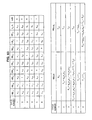
- the value of a coefficient input to the AND circuit 22 is set to be stored in a recording memory (a ROM, a RAM, or the like) in advance in the form shown in, for example, FIG. 13 . For this reason, the value of a desired coefficient can be obtained by accessing a desired address at a desired timing.
- an arithmetic operation circuit can be constructed by one variable generation circuit 31 , a plurality of AND circuits 32 and 35 , a plurality of multipliers 33 and 36 , and a plurality of intermediate value retaining circuits 34 and 37 .
- the variable x i x j or x j generated by the variable generation circuit 31 once is used for an arithmetic operation of the quadratic multivariate polynomials f 1 (x), . . . , f m (x) in a parallel manner.
- b mi are assumed to be stored in the recording memory (the ROM, the RAM, or the like) in advance in the form shown in FIG. 15 .
- the value of a desired coefficient with regard to f 1 (x), . . . , f m (x) can be obtained at once by accessing a desired address at a desired timing.
- the circuit By configuring the circuit as described above, the m quadratic multivariate polynomials f 1 (x), . . . , f m (x) can be calculated in parallel, and thereby the number of processing cycles is reduced.
- description will proceed focusing on one quadratic multivariate polynomials f i .
- the circuit that calculates the m quadratic multivariate polynomials f 1 (x), . . . , f m (x) in a parallel manner can be constructed.
- Reference Literature 2 (Andrey Bogdanov, Thomas Eisenbarth, Andy Rupp, and Christopher Wolf, “Time-Area Optimized Public-Key Engines: MQ-Cryptosystems as Replacement for Elliptic Curves?”, CHES 2008, LNCS 5154, pp. 45-61, 2008.) provides description.
- Reference Literature 2 introduces a circuit configuration that adopts a feedback loop for a shift register.
- the circuit configurations described in Reference Literature 1 and Reference Literature 2 are for calculating a quadratic multivariate polynomial f(x) with respect to one input x ⁇ 0, 1 ⁇ n . For this reason, in order to calculate quadratic multivariate polynomials f(x 1 ) and f(x 2 ) for two inputs x 1 and x 2 ⁇ 0, 1 ⁇ n , it is necessary to operate two arithmetic operation circuits in parallel or one arithmetic operation circuit two times. In addition, as will be described in detail below, the circuit configurations described in Reference Literature 1 and Reference Literature 2 can be improved in terms of a processing speed or a circuit scale.
- the arithmetic operation circuit that uses selectors with multi-bit inputs is constituted by a first circuit part (refer to FIGS. 16 and 17 ) that generates the variable x i x j or x i of each term constituting the quadratic multivariate polynomial f(x) and a second circuit part (refer to FIG. 18 ) that sums intermediate values obtained by multiplying the variable of each term by the coefficient a ij or b j , and then outputs the arithmetic operation result z.
- the register 101 includes registers R 1 , . . . , R n and selectors S 1 , . . . , S n as shown in FIG. 17 .
- the registers R 1 , . . . , R n store x 1 , . . . , x n via the selectors S 1 , . . . , S n respectively at a first cycle.
- x 1 , . . . , x n stored in the registers R 1 , . . . , R n are output as y 1 , . . . , y n at an arbitrary timing.
- the output values y 1 , . . . , y n of the register 101 are input to the selectors 102 and 103 as shown in FIG. 16 .
- the selector 102 selects one value from each of the input values y 1 , . . . , y n and then inputs the values to the AND circuit 104 .
- the selector 103 selects one value from each of the input values y 2 , . . . , y n and a constant “1” and then inputs the values to the AND circuit 104 .
- the AND circuit 104 performs a logical AND operation for the two input values and then outputs x i x j or x i .
- the output value of the AND circuit 104 is input to an AND circuit 105 constituting the second circuit part as shown in FIG. 18 .
- the second circuit part includes an XOR circuit 106 and a register 107 in addition to the AND circuit 105 as shown in FIG. 18 .
- the width of all wirings shown in FIG. 18 is one bit.
- the output value of the AND circuit 104 and the coefficient a ij or b i are input to the AND circuit 105 . Then, the output value (intermediate value) of the AND circuit 105 is input to the XOR circuit 106 .
- the intermediate value and a stored value of the register 107 are input to the XOR circuit 106 .
- the XOR circuit 106 performs an exclusive-OR operation for the two input values, and then inputs the arithmetic operation result (intermediate value) to the register 107 .
- the value stored in the register 107 is output as an arithmetic operation result z.
- the registers R 1 , . . . , R n constituting the register 101 store inputs x ⁇ 0, 1 ⁇ n .
- the succeeding cycle (P2) in the state in which the stored values of the registers R 1 , . . . , R n are retained, the stored values x 1 , . . . , x n of the registers R 1 , . . . , R n are output as y 1 , . . . , y n .
- y n and the constant “1” is executed by the selectors 102 and 103 with inputs of n bits.
- “1” is output from one of the selectors 102 and 103 .
- the arithmetic operation circuit of the quadratic multivariate polynomial f(x) can be constructed by using the selectors with multi-bit inputs.
- the selectors with multi-bit inputs since the selectors with multi-bit inputs are used, the critical path is lengthened and the maximum operation frequency is lowered.
- the selectors with multi-bit inputs are installed, the circuit scale increases.
- an arithmetic operation circuit that calculates the quadratic multivariate polynomial f(x) with regard to a plurality of inputs is constructed by installing arithmetic operation circuits that use selectors with multi-bit inputs in parallel, it is necessary to prepare a plurality of pairs of AND circuits and XOR circuits. These points can be improved.
- the arithmetic operation circuit that uses a shift register does not includes a selector with multi-bit inputs, and can generate intermediate values using an output of a shift register without change, and thus a drop of the maximum operation frequency or an increase of the circuit scale can be suppressed.
- the arithmetic operation circuit that uses a shift register is constituted by a first circuit part (refer to FIGS. 20 and 21 ) that generates the variable x i x j or x i of each term constituting the quadratic multivariate polynomial f(x) and a second circuit part (refer to FIG. 22 ) that sums intermediate values obtained by multiplying the variable of each term by the coefficient a ij or b j and then outputs the arithmetic operation result z.
- the first circuit part includes a shift register 201 and an AND circuit 202 as shown in FIG. 20 .
- the shift register 201 includes selectors S 1 , . . . , S n+1 and registers R 1 , . . . , R n+1 as shown in FIG. 21 .
- the selectors S 1 , . . . , S n+1 are registers of “3-bit input: 1-bit output.”
- the selectors S 2 , . . . , S n are registers of “2-bit input: 1-bit output.”
- the width of all wirings is 1 bit.
- the second circuit part includes an AND circuit 203 , an XOR circuit 204 , a register 205 as shown in FIG. 22 .
- An output value of the AND circuit 202 constituting the first circuit part and coefficient a ij or b i are input to the AND circuit 203 .
- An output value of the AND circuit 203 is input to the XOR circuit 204 .
- the output value of the AND circuit 203 and a stored value in the register 205 are input to the XOR circuit 204 .
- the stored value of the register 205 is updated to an output value of the XOR circuit 204 . Then, when a summation process is completed for all combinations of the inputs x, the stored value of the register 205 is output as an arithmetic operation result z.
- the registers R 1 , . . . , R n constituting the shift register 201 store inputs x ⁇ 0, 1 ⁇ n .
- the register R n+1 stores the value “1.”
- the stored value “1” is used to calculate a first-order term included in the quadratic multivariate polynomial f(x).
- the shift register 201 outputs the stored value as an output value y 1 .
- the shift register 201 outputs the stored value of the registers R 2 as an output value y 2 .
- the stored values are rotated in the registers R 2 , . . . , R n+1 .
- the value x 2 of one bit stored in the registers R 2 is moved to the register R n+1
- the values x 3 , . . . , x n , and 1 of one bit stored in the registers R 3 , . . . , R n+1 are moved to the registers R 2 , . . . , R n .
- the registers R 1 , . . . , R n+1 store values x 1 , x 3 , . . . , x n , 1, x 2 of one bit respectively.
- next cycle (P3) while the stored value of the register R 1 is maintained, the stored value is output from the shift register 201 as the output value y 1 as shown in FIG. 24 .
- the stored value of the register R 2 is output from the shift register 201 as the output value y 2 .
- rotation of the stored values is performed in the registers R 2 , . . . , R n+1 .
- outputs of y 1 and y 2 and rotation of the stored values are repeated.
- the registers R 1 , . . . , R n+1 store the values x 1 , x 2 , . . . , x n , and 1 of one bit respectively
- the stored values are rotated in the registers R 1 , . . . , R n+1 (P6).
- the registers R 1 , . . . , R n+1 are in the state in which each stores the value x 2 , x 3 , . . . , x n , 1, and x 1 of one bit respectively.
- the stored value of the register R1 is maintained again, the stored value is output from the shift register 201 as the output value y 1 .
- the stored value of the register R 2 is output from the shift register 201 as the output value y 2 .
- the stored values are rotated in the registers R 2 , . . . , R n+1 .
- the shift register 201 combines rotation of the stored values in the registers R 2 , . . . , R n+1 and rotation of the stored values of the registers R 1 , . . . , R n+1 and controls the combination of two output values y 1 and y 2 .
- the registers R 1 , . . . , R 5 store inputs x 1 , . . . , x 4 , and 1.
- the stored values x 1 and x 2 are output from the registers R 1 and R 2 as the output values y 1 and y 2 .
- the output values y 1 and y 2 are input to the AND circuit 202 .
- the logical sum y is input to the AND circuit 203 .
- the logical AND with a coefficient a 12 is calculated by the AND circuit 203 , and stored in the register 205 .
- cycle number 2 the stored values are rotated in the registers R 2 , . . . , R 5 , and the stored values are updated to x 3 , x 4 , 1, and x 2 , respectively. For this reason, the output values y 1 and y 2 of the shift register 201 become x 1 and x 3 .
- the stored values are rotated in the registers R 2 , . . . , R 5 , and the shift register 201 outputs the values y 1 and y 2 in each cycle.
- the stored values of the registers R 1 , . . . , R 5 become x 1 , . . . , x 4 , and 1 respectively, and when the stored values are output from the registers R 1 and R 2 as they are, the values x 1 and x 2 that have already been output are output.
- the stored value of the register 205 is retained.
- rotation is performed in the registers R 1 , . . . , R 5 .
- the stored values of the registers R 1 , . . . , R 5 are x 2 , x 3 , x 4 , 1, and x 1 in this order as described in the field of the rotation number 5+1.
- the shift register 201 outputs the stored values from the registers R 1 and R 2 .
- the shift register 201 outputs the stored values from the registers R 1 and R 2 while rotating the stored values of the registers R 2 , . . . , R 5 .
- the stored value of the register 205 is not updated.
- the stored values of the registers R 1 , . . . , R 5 are rotated to array the stored values of the registers R 1 , . . . , R 5 , without updating the stored value of the register 205 .
- the shift register 201 performs rotation of the registers R 2 , . . . , R 5 that causes the output from the registers R 1 and R 2 , rotation of the registers R 2 , . . . , R 5 that does not cause the output from the registers R 1 and R 2 , and rotation of the registers R 1 , . . . , R 5 that does not cause the output from the registers R 1 and R 2 , and then outputs values for all combinations of the stored values.
- the values y 1 and y 2 output from the shift register 201 are summed by the AND circuits 202 and 203 , the XOR circuit 204 , and the register 205 on each occasion.
- the arithmetic operation circuit for the quadratic multivariate polynomial f(x) can be constructed by using the shift register.
- the arithmetic operation circuit for calculating the quadratic multivariate polynomial f(x) with regard to a plurality of inputs is constructed by parallel-installing circuits using the exemplified arithmetic operation circuit herein, it is necessary to prepare a plurality of pairs of AND circuits and XOR circuits. This point can be improved.
- This configuration uses a plurality of feedback loops and enables rotation executed only for arraying an order of storage values to be avoided.
- the arithmetic operation circuit that uses a shift register is constituted by a first circuit part (refer to FIGS. 27 and 28 ) for generating the variable x i x j or x i of each term constituting the quadratic multivariate polynomial f(x) and a second circuit part (refer to FIG. 29 ) that sums intermediate values obtained by multiplying the variable of each term by the coefficient a ij or b j and outputting the arithmetic operation result z.
- the first circuit part mainly includes a shift register 301 and an AND circuit 302 as shown in FIG. 27 .
- a mask circuit 303 (refer to FIG. 29 ) provided in the front stage of the AND circuit 302 is omitted for the sake of convenience in order to facilitate comparison to the shift register 201 shown in FIG. 20 .
- the shift register 301 includes the selectors S 1 , . . . , S n and the registers R 1 , . . . , R n as shown in FIG. 28 .
- the selector S 1 is a register of “3-bit input: 1-bit output.”
- the selectors S 2 , . . . , S n are registers of “4-bit input: 1-bit output.”
- the width of all wirings is 1 bit.
- the second circuit part includes an AND circuit 304 , an XOR circuit 305 , and a register 306 as shown in FIG. 29 .
- the mask circuit 303 outputs 1 regardless of the value of the input y 2 .
- the mask circuit 303 outputs the value of the input y 2 without change.
- the output value of the mask circuit 303 is input to the AND circuit 302 .
- the one value y 1 output from the shift register 301 and the output value of the mask circuit 303 are input to the AND circuit 302 .
- the output value of the AND circuit 302 constituting the first circuit part and the coefficient a ij or b i are input to the AND circuit 304 .
- the output value of the AND circuit 304 is input to the XOR circuit 305 .
- the output value of the AND circuit 304 and the stored value in the register 306 are input to the XOR circuit 305 .
- the stored value of the register 306 is updated to the output value of the XOR circuit 306 . Then, when a summation process for all combinations of inputs x is completed, the stored value of the register 306 is output as an arithmetic operation result z.
- the registers R 1 , . . . , R n constituting the shift register 201 store inputs x ⁇ 0, 1 ⁇ n .
- the shift register 201 outputs the stored value as an output value y 1 .
- the shift register 201 outputs the stored value of the registers R 2 as an output value y 2 .
- rotation of stored values is performed in the registers R 2 , . . . , R n .
- the value x 2 of one bit stored in the registers R 2 is moved to the register R n , and the values x 3 , . . . , x x , of one bit stored in the registers R 3 , . . . , R n are moved to the registers R 2 , . . . , R n ⁇ 1 .
- the registers R 1 , . . . , R n store values x 1 , x 3 , . . . , x n , and x 2 of one bit respectively.
- next cycle (P3) while the stored value of the register R1 is maintained, the stored value is output from the shift register 301 as the output value y 1 as shown in FIG. 31 .
- the stored value of the register R 2 is output from the shift register 301 as the output value y 2 .
- rotation of the stored values is performed in the registers R 2 , . . . , R n .
- outputs of y 1 and y 2 and rotation of the stored values are repeated.
- the registers R 1 , . . . , R n store the values x 1 , x 2 , . . . , x n of one bit respectively.
- the stored values are rotated in the registers R 1 , . . . , R n (P5).
- the shift register 301 outputs the stored values from the registers R 1 and R 2 .
- the pair of the output stored values x 1 and x 2 has already been output, but the value x 2 (y 2 ) is masked by setting the mask value to be 1, and then the value x 1 (y 1 ) and the value “1” are input to the AND circuit 302 .
- the registers R 1 , . . . , R n are in the state in which each stores the value x 2 , x 3 , . . . , x n , and x 1 of one bit respectively (P6).
- the stored value of the register R 1 is maintained again, the stored value is output from the shift register 301 as the output value y 1 .
- the stored value of the register R 2 is output from the shift register 301 as the output value y 2 .
- the stored value of R n in which x 1 is stored is also maintained. Based on this, rotation of the stored values is performed in the registers R 2 , . . . , R n ⁇ 1 . Then, when the process of generating a term relating to the variable x 2 is finished, rotation of the stored values is performed in the registers R 1 , . .
- a difference between the shift register 201 previously described and the shift register 301 is that there is no period in which cycles are spent only for arraying the stored values of the registers R 1 , . . . , R n . This matter will be reviewed in more detail with reference to a specific example.
- a specific operation of the arithmetic operation circuit will be described with reference to FIG. 33 .
- the first cycle (cycle number 1), inputs x 1 , . . . , x 4 are input to the registers R 1 , . . . , R 4 .
- the stored values x 1 and x 2 are output from the registers R 1 and R 2 as the output values y 1 and y 2 .
- the output values y 1 and y 2 are respectively input to the AND circuit 302 and the mask circuit 303 .
- the logical sum y is input to the AND circuit 304 .
- the logical AND with a coefficient a 12 is calculated by the AND circuit 304 and then stored in the register 306 .
- the stored values of the registers R 1 , . . . , R 4 respectively turn into x 1 , . . . , x 4 , and when the stored values are output from the registers R 1 and R 2 without change, the values x 1 and x 2 which have already been output are output.
- the stored values of the registers R 1 , . . . , R 4 are respectively x 2 , x 3 , x 4 , and x 1 in this order as described in the field of the cycle number 4+1.
- the shift register 301 retains the stored values of the registers R 1 , . . . , R 4 and performs rotation of the registers R 1 , . . . , R 4 while switching the setting of the mask value mask, and then outputs values with regard to all combinations of the stored values.
- the values y 1 and y 2 output from the shift register 301 are summed by the mask circuit 303 , the AND circuits 302 and 304 , the XOR circuit 305 , and the register 306 on each occasion. Then, when the summation of all combinations that can be selected from the values x 1 , . . . , x 4 is completed, the stored value of the register 306 is output from the arithmetic operation circuit as the arithmetic operation result z.
- the arithmetic operation circuit of the quadratic multivariate polynomial f(x) can be constructed by using a shift register.
- a useless cycle for performing rotation without outputting a value to array an order of stored values as described above is no longer necessary.
- a configuration of a control device 310 that controls the selectors S 1 , . . . , S n with multi-bit inputs constituting the shift register 301 becomes complicated. As a result, an expansion of a circuit scale and an increase in the critical path occur.
- Embodiment #1 a configuration of an arithmetic operation circuit that can be used in calculation of a quadratic multivariate polynomial F(x) (calculation of f(x) constituting F(x)) (Embodiment #1) will be described.
- the arithmetic operation circuit according to Embodiment #1 is designed to enable execution of calculation of quadratic multivariate polynomials F(x 1 ) and F(x 2 ) (calculation of f(x 1 ) and f(x 2 )) in parallel with respect to two inputs x 1 and x 2 .
- the arithmetic operation circuit according to Embodiment #1 is constituted by a shift register 401 , AND circuits 402 and 403 , a selector 404 , an AND circuit 405 , an XOR circuit 406 , selectors 407 and 409 , registers 408 and 410 , and a selector 411 .
- the shift register 401 includes a first shift register 4011 and a second shift register 4012 .
- a configuration of the first shift register 4011 is substantially the same as that of the shift register 201 shown in FIG. 21 .
- a configuration of the second shift register 4012 is substantially the same as that of the shift register 201 shown in FIG. 21 except that combinations of registers that output values are different.
- the first shift register 4011 and the second shift register 4012 are operated in association with each other in the same cycles.
- the first shift register 4011 is constituted by registers R 1,1 , . . . , R 1,n+1 and selectors S 1,1 , . . . , S 1,n+1 .
- the first shift register 4011 is configured to output stored values from the registers R 1,1 and R 1,2 .
- the second shift register 4012 is constituted by registers R 2,1 , . . . , R 2,n+1 and selectors S 2,1 , . . . , S 2,n+1 .
- the second shift register 4012 is configured to output stored values from the registers R 2,1 and R 2,n+1 .
- Values y 1,1 and y 1,2 output from the first shift register 4011 are input to the AND circuit 402 as shown in FIG. 36 .
- values y 2,1 and y 2,2 output from the second shift register 4012 are input to the AND circuit 403 .
- the AND circuit 402 computes the logical AND of the input values y 1,1 and y 1,2 and inputs the computation result to the selector 404 .
- the AND circuit 403 computes the logical AND of the input values y 2,1 and y 2,2 and inputs the computation result to the selector 404 .
- the selector 404 selects one value from the two input values, and then inputs the selection result to the AND circuit 405 .
- the output value of the selector 404 and the coefficients a ij and b i are input to the AND circuit 405 .
- the AND circuit 405 computes the logical AND of the input output value and the coefficients, and then inputs the computation result to the XOR circuit 406 .
- the output value of the AND circuit 405 and the output value of the selector 411 that will be described later are input to the XOR circuit 406 .
- the XOR circuit 406 executes an exclusive-OR operation for the two input values, and then inputs the arithmetic operation result to the selectors 407 and 409 .
- the arithmetic operation result is stored in the register 408 or the register 410 according to the state of the selectors 407 and 409 .
- either of the stored values of the registers 408 and 410 is input to the XOR circuit 406 or both are output from the arithmetic operation circuit as the arithmetic operation result z according to the state of the selector 4
- the portions in which wirings are indicated by dashed lines in the drawing represent control over signals not to substantially flow in corresponding cycles.
- the portions in which wirings are indicated by solid lines in the drawing represent control over signals to flow in corresponding cycles.
- the control of the signal paths is realized by controlling the selectors S 1,1 , . . . , S 1,n , S 2,1 , . . . , S 2,n+1 , the selector 404 , the selector 407 , the selector 409 , and the selector 411 .
- the registers R 1,1 , . . . , R 1,n store input values x 1,1 , . . . , x 1,n as shown in FIG. 37 .
- the register R 1,n+1 stores the value “1.”
- the value “1” stored here is used to calculate a first-order term included in the quadratic multivariate polynomials f(x 1 ).
- the registers R 2,1 , . . . , R 2,n store input values x 2 , . . . , x 2,1 (the reverse order should be noted).
- the register R 2,n+1 stores the value “1.”
- the value “1” stored here is used to calculate a first-order term included in the quadratic multivariate polynomials f(x 2 ).
- the stored values x 1,1 and x 1,2 stored in the registers R 1,1 and R 1,2 are output as output values y 1,1 and y 1,2 as shown in FIG. 38 .
- the stored value of the register R 1,1 is retained, and the stored values of the registers R 1,2 , . . . , R 1,n+1 are rotated.
- the value x 1,2 of one bit stored in the register R 1,2 is moved to the register R 1,n+1 and the values x 1,3 , . . . , x 1,n , and 1 of one bit stored in the registers R 1,3 , . . . , R 1,n+1 are moved to the registers R 1,2 , . .
- the registers R 1,1 , . . . , R 1,n+1 are in the state in which the values x 1,1 , x 1,3 , . . . , x 1,n , 1, and x 1,2 of one bit are respectively stored.
- the stored value of the register R 2,1 is retained, and the stored values of the registers R 2,2 , . . . , R 2,n+1 are rotated.
- a value x 2,n ⁇ 1 of one bit stored in the register R 2,2 is moved to the register R 2,n+1 , and values x 2, n ⁇ 2 , . . . , x 2,1 , and 1 of one bit stored in the registers R 2,3 , . . . , R 2,n+1 are moved to the registers R 2,2 , . . . , R 2,n .
- R 2,n+1 are in the state in which values x 2,n , x 2, n ⁇ 2 , . . . , x 2,1 , 1, and x 2,n ⁇ 1 of one bit are respectively stored.
- the stored values of the registers R 2,1 and R 2,n+1 are not output from the shift register 401 (actually, an output value of the AND circuit 402 is selected by the selector 404 ).
- the values y 1,1 and y 1,2 output from the shift register 401 are input to the AND circuit 402 as shown in FIG. 39 .
- the value of the logical AND output from the AND circuit 402 is input to the selector 404 .
- the selector 404 is controlled such that the output value of the AND circuit 402 is selected.
- the value input to the selector 404 is input to the AND circuit 405 as an output value y of the selector 404 , and multiplied by a coefficient.
- the output of the AND circuit 405 is input to the XOR circuit 406 .
- the value input to the XOR circuit 406 is input to the selectors 407 and 409 .
- the selector 409 blocks a path connecting the output of the XOR circuit 406 and connects a path connecting the output of the register 410 .
- the output value of the XOR circuit 406 is stored in the register 408 via the selector 407 connected to the output of the XOR circuit 406 .
- control is performed such that the input of the selector 404 is connected to the output of the AND circuit 402 , the output of the XOR circuit 406 is connected to the input of the selector 407 in the cycle in which the first shift register 4011 outputs a stored value, and the input of the selector 409 is connected to the output of the register 410 .
- the selector 411 is maintained in the state in which the output of the register 408 is connected to the input of the XOR circuit 406 . While this state is maintained, the shift register 401 outputs the stored values of the registers R 1,1 and R 1,2 , rotating the stored values of the registers R 1,2 , . . . , R 1,n+1 and the registers R 2,2 , . . . , R 2,n+1 . Then, each time a value is output from the shift register 401 , intermediate values are summed via the AND circuit 402 , the selector 404 , the XOR circuit 406 , and the selector 407 , and thereby the stored value of the register 408 is updated.
- the input of the selector 404 is controlled such that it is connected to the output of the AND circuit 403 .
- the input of the selector 407 is controlled such that it is connected to the output of the register 408 .
- the input of the selector 409 is controlled such that it is connected to the output of the XOR circuit 406 .
- the input of the selector 411 is controlled such that it is connected to the output of the register 410 .
- the output value of the AND circuit 403 is input to the AND circuit 405 via the selector 404 .
- the output value of the AND circuit 405 is stored in the register 410 via the XOR circuit 406 and the selector 409 .
- the arithmetic operation circuit processes the output value of the second shift register 4012 at the timing at which rotation with regard to the registers R 1,2 , . . . , R 1,n+1 and rotation with regard to the registers R 1,1 , . . . , R 1,n+1 are performed in order for the first shift register 4011 to array the stored values.
- the selectors 404 , 407 , 409 , and 411 are controlled to cause the signal path to return to the original state.
- a process of outputting the stored values of the registers R 1,1 and R 1,2 is performed while the stored values of the registers R 1,2 , . . . , R 1,n+1 are rotated.
- the registers R 1,1 , . . . , R 1,5 store inputs x 1,1 , . . . , x 1,4 , and 1.
- the registers R 2,1 , . . . , R 2,5 store inputs x 2,4 , . . . , x 2,1 , and 1.
- the stored values x 1,1 and x 1,2 are output from the registers R 1,1 and R 1,2 as the output values y 1,1 and y 1,2 .
- the stored values x 2,1 and 1 are output from the registers R 2,1 and R 2,5 as the output values y 2,1 and y 2,2 .
- the selector 404 chooses the outputs of the AND circuit 402 . Note that detailed processes in the later stage of the selector 404 will not be provided.
- the stored values are rotated in the registers R 1,2 , . . . , R 1,5 , and the stored values are respectively updated to x 1,3 , x 1,4 , 1, and x 1,2 .
- the output values y 1,1 and y 1,2 of the shift register 401 respectively turn into x 1,1 and x 1,3 .
- the stored values are rotated in the registers R 2,2 , . . . , R 2,5 , and the stored values are respectively updated to x 2,2 , x 2,1 , 1, and x 2,3 .
- the stored values are rotated in the registers R 1,2 , . . . , R 1,5 , and R 2,2 , . . . , R 2,5 , and the values y 1,1 and y 1,2 are output from the shift register 401 in each cycle.
- the stored values of the registers R 1,1 , . . . , R 1,5 respectively turn into x 1,1 , . . . , x 1,4 , and 1, and the stored values are output from the registers R 1,1 and R 1,2 without change, the values x 1,1 and x 1,2 that have already been output are output.
- the shift register 401 performs rotation in the registers R 1,1 , . . . , R 1,5 without outputting a value from the registers R 1,1 and R 1,2 .
- the shift register 401 outputs the stored values from the registers R 2,1 and R 2,5 .
- the selector 404 chooses the output of the AND circuit 403 .
- the stored values of the registers R 1,1 , . . . , R 1,5 are arrayed in the order of x 1,2 , x 1,3 , x 1,4 , 1, and x 1,1 as described in the field of the cycle number 5+1.
- the stored values of the registers R 2,1 , . . . , R 2,5 are arrayed in the order of x 2,3 , x 2,2 , x 2,1 , 1, and x 2,4 . Note that, in the cycles numbers 5+1 to 5+3, the selector 404 chooses the output of the AND circuit 402 again.
- the first shift register 4011 performs rotation of the stored values in the registers R 1,2 , . . . , R 1,5 .
- the stored values are output from the registers R 1,1 and R 1,2 .
- the shift register 401 rotates the stored values of the registers R 1,1 , . . . , R 1,5 to array the stored values of the registers R 1,1 , . . . , R 1,5 without outputting a value from the registers R 1,1 and R 1,2 as in the cycle number 5.
- the second shift register 4012 performs rotation of the stored vales of the registers R 2,2 , . . . , R 2,5 in the cycles numbers 5+1 to 5+4.
- the stored values are output from the registers R 2,1 and R 2,5 .
- the cycle number 2 ⁇ 5 the stored values are output from the registers R 2,1 and R 2,5 while the stored values of the registers R 2,1 , . . . , R 2,5 are rotated.
- the selector 404 chooses the output of the AND circuit 403 .
- the shift register 401 performs rotation accompanied with an output from the registers R 1,1 and R 1,2 and rotation accompanied with an output from the registers R 2,1 and R 2,5 and then outputs values with regard to all combinations of the stored values. Then, when the summation is completed for all combinations that can be selected from the values x 1,1 , . . . , x 1,4 , and 1, and all combinations that can be selected from the values x 2,4 , . . . , x 2,1 , and 1, the stored values are respectively output from the registers 408 and 410 as the arithmetic operation result z.
- control over the selectors 404 , 407 , 409 , and 411 is performed by a control unit (not illustrated) provided in the arithmetic operation circuit or a control device (not illustrated) provided in the outside of the arithmetic operation circuit.
- the input of the selector 404 is connected to the output of the AND circuit 402 .
- the input of the selector 407 is connected to the output of the XOR circuit 406 .
- the input of the selector 409 is connected to the output of the register 410 .
- the input of the selector 411 is connected to the output of the register 408 .
- the input of the selector 404 is connected to the output of the AND circuit 403 .
- the input of the selector 409 is connected to the output of the XOR circuit 406 .
- the input of the selector 407 is connected to the output of the register 408 .
- the input of the selector 411 is connected to the output of the register 410 .
- coefficients that are subject to an arithmetic operation for the output of the AND circuit 403 are denoted by giving primes for the sake of convenience, but the same coefficients as those that are subject to an arithmetic operation for the output of the AND circuit 402 may be used.
- the arithmetic operation circuit according to Embodiment #1 since the arithmetic operation circuit according to Embodiment #1 uses the shift registers, it does not include a selector with multi-bit inputs. In addition, the arithmetic operation circuit only includes two kinds of feedback loops of the shift registers. Furthermore, since, at a timing at which one shift register arrays stored values of registers, the other shift register outputs stored values, the arithmetic operation circuit does not spend cycles only for arraying the stored values. In addition, the two shift registers share AND circuits for multiplying coefficients and the XOR circuit for summation. As a result, an increase in the critical path and an expansion of the circuit scale are suppressed and accordingly a small-sized arithmetic operation circuit that performs arithmetic operations at a high speed is realized.
- Embodiment #2 a configuration of an arithmetic operation circuit that can be used in calculation of quadratic multivariate polynomials F(x 1 ) and G(x 2 , x 3 ) (Embodiment #2) will be described.
- the arithmetic operation circuit according to Embodiment #2 is designed to execute calculation of the quadratic multivariate polynomials F(x 1 ) and G(x 2 , x 3 ) (calculation of f(x 1 ) and g(x 2 , x 3 )) in parallel with regard to three inputs x 1 , x 2 , and x 3 .
- the arithmetic operation circuit according to Embodiment #2 is constituted by a shift register 501 , AND circuits 502 , 503 , and 504 , an XOR circuit 505 , a selector 506 , an AND circuit 507 , an XOR circuit 508 , selectors 509 and 511 , registers 510 and 512 , and a selector 513 .
- the shift register 501 includes a first shift register 5011 , a second shift register 5012 , and a third shift register 5013 .
- first shift register 5011 is substantially the same as that of the first shift register 4011 according to Embodiment #1 described above.
- configurations of the second shift register 5012 and the third shift register 5013 are substantially the same as that of the second shift register 4012 according to Embodiment #1 described above. Thus, detailed description of the configurations will not be provided. Note that the first shift register 5011 , the second shift register 5012 , and the third shift register 5013 are operated in association with each other in the same cycles.
- the significant difference between the arithmetic operation circuit according to Embodiment #1 and the arithmetic operation circuit according to Embodiment #2 is that the number of shift registers included in the shift register 501 described above and the configuration of the XOR circuit 505 .
- the configuration of the arithmetic operation circuit according to Embodiment #2 will be described focusing on the difference.
- the difference is added to calculate the quadratic multivariate polynomial g(x 2 , x 3 ).
- quadratic multivariate polynomials f(x 1 ) that is subject to an arithmetic operation is also expressed as in formula (14) provided below
- quadratic multivariate polynomial g(x 2 , x 3 ) is expressed as in formula (15) provided below.
- the second shift register 5012 , the third shift register 5013 , and the AND circuit 503 are provided to compute x 2i x 3j
- the second shift register, the third shift register 5013 , and the AND circuit 504 are provided to compute x 2j x 3i
- the XOR circuit 505 is provided to add up the computation results.
- the second shift register 5012 and the third shift register 5013 output stored values of the registers in the same cycle.
- the output of the XOR circuit 505 is input to the AND circuit 507 via the selector 506 in the cycle. Note that, since configurations of the circuits provided in the later stage of the AND circuit 507 are substantially the same as that of the arithmetic operation circuit according to Configuration Example #2, description thereof will not be provided.
- Embodiment #2 the configuration of the arithmetic operation circuit according to Embodiment #2 has been described.
- the arithmetic operation circuit according to Embodiment #2 is easily understood considering that the second shift register 4012 in the arithmetic operation circuit according to Embodiment #1 is switched to the second shift register 5012 and the third shift register 5013 and the AND circuit 403 is switched to the set of the AND circuit 503 and 504 and XOR circuit 505 .
- Embodiment #2 an operation of the arithmetic operation circuit according to Embodiment #2 will be described with reference to FIGS. 45 to 50 .
- the operation of the arithmetic operation circuit according to Embodiment #2 is the same as that of the arithmetic operation circuit according to Embodiment #1, detailed description thereof will be omitted and description will proceed focusing on differences.
- control over signal paths is realized by controlling selectors S 1,1 , . . . , S 1,n , S 2,1 , . . . , S 2,n+1 , S 3,1 , . . . , S 3,n+1 and the selector 506 , the selector 509 , the selector 511 , and the selector 513 .
- the operations of the first shift register 5011 and the second shift register 5012 are focused, it is ascertained that they are substantially the same as those of the first shift register 4011 and the second shift register 4012 according to Embodiment #1 as shown in FIGS. 45, 46, and 48 .
- the operation of the third shift register 5013 is the same as that of the second shift register 5012 .
- the input of the selector 506 is connected to the output of the AND circuit 502 in the cycle in which the first shift register 5011 outputs a value as shown in FIG. 47 , the operations are the same as those of the arithmetic operation circuit according to Embodiment #1.
- the input of the selector 506 is connected to the output of the XOR circuit 505 .
- the output values of the second shift register 5012 and the third shift register 5013 are respectively input to the AND circuits 503 and 504
- the output values of the AND circuits 503 and 504 are input to the XOR circuit 505
- the output value of the XOR circuit 505 is input to the AND circuit 507 via the selector 506 .
- operations of the circuits positioned in the later stage of the AND circuit 507 are substantially the same as in the arithmetic operation circuit according to Embodiment #1.
- the arithmetic operation circuit according to Embodiment #2 efficiently generates the terms of the quadratic multivariate polynomial f(x 1 ) expressed in formula (14) above and the terms of the quadratic multivariate polynomial g(x 2 , x 3 ) expressed in formula (15) above. In this manner, when the arithmetic operation circuit according to Embodiment #2 is used, an arithmetic operation of a multivariate polynomial necessary for applying the public-key authentication scheme and the digital signature scheme previously described can be realized.
- arithmetic operation circuits described above enables a reduction of a circuit scale and improvement of a processing speed that take the problem of solving a multivariate polynomial as the base of security to be achieved.
- the probability of successful false proof can be reduced enough to be negligible by calculating the arithmetic operation of quadratic polynomials f(x 1 ) and f(x 2 ) for each of x 1 and x 2 a plurality of times (for example, 140 times) and increasing the number of repetitions of the interactive protocol.
- FIG. 83 is an illustrative diagram showing an example in which a plurality of arithmetic operation circuits 401 shown in FIG. 35 are disposed in parallel. As shown in FIG.
- FIG. 51 is an illustrative diagram showing an example of a data structure of the recording memory.
- FIG. 51 is an illustrative diagram showing the example of the data structure of the recording memory to which an arithmetic operation circuit with a 4-bit and 4-stage pipeline that will be described later refers.
- the plurality of arithmetic operation circuits that execute the arithmetic operation process for the quadratic polynomials are disposed in parallel, it is not necessary to have addresses double due to having the data structure shown in FIG. 51 . This is because the addresses gradually increase when the arithmetic operation process is performed and when the process reaches the final address, the addresses may decrease.
- FIG. 52 is an illustrative diagram showing a configuration of an arithmetic operation circuit according to Embodiment #3.
- the arithmetic operation circuit shown in FIG. 52 performs an arithmetic operation on a quadratic polynomial and outputs values when an input x is 4-bit.
- the arithmetic operation circuit according to Embodiment #3 is configured to include arithmetic operation circuits 600 a , 600 b , 600 c , and 600 d and a ROM 690 that stores coefficients.
- the ROM 690 is divided into two regions 690 a and 690 b.
- the arithmetic operation circuits 600 a , 600 b , 600 c , and 600 d are circuits that generate the quadratic multivariate polynomials f(x 1 ) and f(x 2 ) in parallel from the two inputs x 1 and x 2 .
- the arithmetic operation circuits according to Embodiments #1 and #2 are designed to execute calculation of the quadratic multivariate polynomials f(x 1 ) and f(x 2 ) in parallel for the two inputs x 1 and x 2 with one circuit.
- the pipeline process is a process of connecting processing elements in series so that the output of a processing element is connected to the input of the next processing element, and the pipelined processing elements are parallelized to perform a process.
- FIG. 53 is an illustrative diagram showing an example of a data structure of the ROM 690 and showing examples of coefficients stored in the regions 690 a and 690 b.
- arithmetic operation circuits 600 a and 600 d refer to the coefficients stored in the region 690 a and arithmetic operation circuits 600 b and 600 c refer to the coefficients stored in the region 690 b .
- a drop of the maximum operation frequency can be prevented and higher speed-up of the arithmetic operation process for quadratic polynomials can be achieved.
- FIGS. 54 and 55 are illustrative diagrams showing a circuit configuration of the arithmetic operation circuit 600 a .
- the arithmetic operation circuit 600 a is constituted by a shift register 601 a , AND circuits 602 a and 603 a , a selector 604 a , an AND circuit 605 a , an XOR circuit 606 a , selectors 607 a and 609 a , registers 608 a and 610 a , and a selector 611 a .
- the shift register 601 a includes a first shift register 6011 a and a second shift register 6012 a.
- Configurations of the first shift register 6011 a and the second shift register 6012 a are substantially the same as those of the first shift register 4011 and the second shift register 4012 shown in FIG. 35 except for the difference in combinations of registers that output values. However, the first shift register 6011 a and the second shift register 6012 a are operated in association with each other in the same cycles.
- the first shift register 6011 a is constituted by registers RA 1,1 , RA 1,2 , RA 1,3 , RA 1,4 , and RA 1,5 , and selectors SA 1,1 , SA 1,2 , SA 1,3 , SA 1,4 , and SA 1,5 .
- the first shift register 6011 a is configured to output stored values from the registers RA 1,1 , RA 1,2 , and RA 1,3 .
- the second shift register 6012 a is constituted by registers RA 2,1 , RA 2,2 , RA 2,3 , RA 2,4 , and RA 2,5 , and selectors SA 2,1 , SA 2,2 , SA 2,3 , SA 2,4 , and SA 2,5 .
- the second shift register 6012 a is configured to output stored values from the registers RA 2,1 , RA 2,2 , RA 2,3 , and RA 2,5 .
- Values ya 1,1 , ya 1,2 , and ya 1,3 output from the first shift register 6011 a are input to the arithmetic operation circuit 600 b provided in the later stage.
- the values ya 1,1 and ya 1,2 output from the first shift register 6011 a are input to the AND circuit 602 a as shown in FIG. 55 .
- values ya 2,1 , ya 2,2 , ya 2,3 , and ya 2,5 output from the second shift register 6012 a are input to the arithmetic operation circuit 600 b provided in the later stage.
- the values ya 2,1 and ya 2,5 output from the second shift register 6012 a are input to the AND circuit 603 a .
- the AND circuit 602 a computes the logical AND of the input values ya 1,1 and ya 1,2 and inputs the computation result to the selector 604 a .
- the AND circuit 603 a computes the logical AND of the input values ya 2,1 and ya 2,5 and inputs the computation result to the selector 604 a .
- the selector 604 a selects one value from the two input values and inputs the selection result to the AND circuit 605 a.
- Coefficients a ij and b i and the output value of the selector 604 a are input to the AND circuit 605 a .
- the AND circuit 605 a computes the logical AND of the input output value and the coefficients, and then inputs the computation result to the XOR circuit 606 a .
- the output value of the AND circuit 605 a and the output value of the selector 611 a that will be described later are input to the XOR circuit 606 a .
- the XOR circuit 606 a performs an exclusive-OR operation for the two input values, and then inputs the arithmetic operation result to the selectors 607 a and 609 a .
- the arithmetic operation result is stored in the register 608 a or the register 610 a according to states of the selectors 607 a and 609 a .
- either stored value of the register 608 a or 610 a is input to the XOR circuit 606 a or output from the arithmetic operation circuit 600 a as arithmetic operation results za 1 and za 2 according to a state of the selector 611 a .
- the values za 1 and za 2 from the registers 608 a and 610 a are input to the arithmetic operation circuit 600 b provided in the later stage.
- selectors 604 a and 611 a select and output one of the input values according to the value of selA that will be described later.
- FIGS. 56 and 57 are illustrative diagrams showing a circuit configuration of the arithmetic operation circuit 600 b .
- the arithmetic operation circuit 600 b is constituted by a shift register 601 b , AND circuits 602 b and 603 b , a selector 604 b , an AND circuit 605 b , an XOR circuit 606 b , selectors 607 b and 609 b , registers 608 b and 610 b , and a selector 611 b .
- the shift register 601 b includes a first shift register 6011 b and a second shift register 6012 b.
- a configuration of the first shift register 6011 b has one less register than the configuration of the first shift register 6011 a shown in FIG. 54 .
- a configuration of the second shift register 6012 b is substantially the same as that of the second shift register 6012 a shown in FIG. 54 except that combinations of the registers that output values are different. However, the first shift register 6011 b and the second shift register 6012 b are operated in association with each other in the same cycles.
- the first shift register 6011 b is constituted by registers RB 1,1 , RB 1,2 , RB 1,3 , and RB 1,4 , and selectors SB 1,1 , SB 1,2 , SB 1,3 , and SB 1,4 .
- the first shift register 6011 b is configured to output stored values from the registers RB 1,1 , and RB 1,2 .
- the second shift register 6012 b is constituted by registers RB 2,1 , RB 2,2 , RB 2,3 , RB 2,4 , and RB 2,5 , and selectors SB 2,1 , SB 2,2 , SB 2,3 , SB 2,4 , and SB 2,5 .
- the second shift register 6012 b is configured to output stored values from the registers RB 2,1 , RB 2,2 , RB 2,4 , and RB 2,5 .
- Values yb 1,1 , and yb 1,2 output from the first shift register 6011 b are input to the arithmetic operation circuit 600 c provided in the later stage.
- the values yb 1,1 , and yb 1,2 output from the first shift register 6011 b are input to the AND circuit 602 b as shown in FIG. 57 .
- values yb 2,1 , yb 2,2 , yb 2,4 , and yb 2,5 output from the second shift register 6012 b are input to the arithmetic operation circuit 600 c provided in the later stage.
- the values yb 2,1 and yb 2,5 output from the second shift register 6012 b are input to the AND circuit 603 b .
- the AND circuit 602 b computes the logical AND of the input values yb 1,1 and yb 1,2 and inputs the computation result to the selector 604 b .
- the AND circuit 603 b computes the logical AND of the input values yb 2,1 and yb 2,5 and inputs the computation result to the selector 604 b .
- the selector 604 b selects one value from the two input values and inputs the selection result to the AND circuit 605 b.
- the coefficients a ij and b i and the output value of the selector 604 b are input to the AND circuit 605 b .
- the AND circuit 605 b computes the logical AND of the input output value and the coefficients, and then inputs the computation result to the XOR circuit 606 b .
- the output value of the AND circuit 605 b and the output value of the selector 611 b that will be described later are input to the XOR circuit 606 b .
- the XOR circuit 606 b performs an exclusive-OR operation for the two input values, and then inputs the arithmetic operation result to the selectors 607 b and 609 a .
- the arithmetic operation result is stored in the register 608 b or the register 610 b according to states of the selectors 607 b and 609 b .
- either stored value of the register 608 b or 610 b is input to the XOR circuit 606 b or output from the arithmetic operation circuit as arithmetic operation results zb 1 and zb 2 according to a state of the selector 611 b .
- the values zb 1 and zb 2 from the registers 608 b and 610 b are input to the arithmetic operation circuit 600 c provided in the later stage.
- the selectors 604 b and 611 b select and output one of the input values according to the value of selB that will be described later.
- the selector 607 b selects and outputs one of the output of the XOR circuit 606 b , the value za 1 supplied from the arithmetic operation circuit 600 a , and the output of the register 608 b .
- the selector 609 b selects and outputs one of the output of the XOR circuit 606 b , the value za 2 supplied from the arithmetic operation circuit 600 a , and the output of the register 610 b.
- FIGS. 58 and 59 are illustrative diagrams showing a circuit configuration of the arithmetic operation circuit 600 c .
- the arithmetic operation circuit 600 c is constituted by a shift register 601 c , AND circuits 602 c and 603 c , a selector 604 c , an AND circuit 605 c , an XOR circuit 606 c , selectors 607 c and 609 c , registers 608 c and 610 c , and a selector 611 c .
- the shift register 601 c includes a first shift register 6011 c and a second shift register 6012 c.
- a configuration of the first shift register 6011 c has one less register than the configuration of the first shift register 6011 b shown in FIG. 56 .
- a configuration of the second shift register 6012 c is substantially the same as that of the second shift register 6012 a shown in FIG. 54 except that combinations of the registers that output values are different. However, the first shift register 6011 c and the second shift register 6012 c are operated in association with each other in the same cycles.
- the first shift register 6011 c is constituted by registers RC 1,1 , RC 1,2 , and RC 1,3 , and selectors SC 1,1 , SC 1,2 , and SC 1,3 .
- the first shift register 6011 c is configured to output stored values from the registers RC 1,1 , and RC 1,2 .
- the second shift register 6012 c is constituted by registers RC 2,1 , RC 2,2 , RC 2,3 , RC 2,4 , and RC 2,5 , and selectors SC 2,1 , SC 2,2 , SC 2,3 , SC 2,4 , and SC 2,5 .
- the second shift register 6012 c is configured to output stored values from the registers RC 2,1 , RC 2,3 , RC 2,4 , and RC 2,5 .
- a value yc 1,1 output from the first shift register 6011 c is input to the arithmetic operation circuit 600 d provided in the later stage.
- the values yc 1,1 , and yc 1,2 output from the first shift register 6011 c are input to the AND circuit 602 c as shown in FIG. 59 .
- values yc 2,1 , yc 2,3 , yc 2,4 , and yc 2,5 output from the second shift register 6012 c are input to the arithmetic operation circuit 600 d provided in the later stage.
- the values yc 2,1 and yc 2,5 output from the second shift register 6012 c are input to the AND circuit 603 c .
- the AND circuit 602 c computes the logical AND of the input values yc 2,1 and yc 1,2 and inputs the computation result to the selector 604 c .
- the AND circuit 603 c computes the logical AND of the input values yc 2,1 and yc 2,5 and inputs the computation result to the selector 604 c .
- the selector 604 c selects one value from the two input values and inputs the selection result to the AND circuit 605 c.
- the coefficients a ij and b i and the output value of the selector 604 c are input to the AND circuit 605 c .
- the AND circuit 605 c computes the logical AND of the input output value and the coefficients, and then inputs the computation result to the XOR circuit 606 c .
- the output value of the AND circuit 605 c and the output value of the selector 611 c that will be described later are input to the XOR circuit 606 c .
- the XOR circuit 606 c performs an exclusive-OR operation for the two input values, and then inputs the arithmetic operation result to the selectors 607 c and 609 c.
- the arithmetic operation result is stored in the register 608 c or the register 610 c according to states of the selectors 607 c and 609 c .
- either stored value of the register 608 c or 610 c is input to the XOR circuit 606 c or output from the arithmetic operation circuit as arithmetic operation results zc 1 and zc 2 according to a state of the selector 611 c .
- the values zc 1 and zc 2 from the registers 608 c and 610 c are input to the arithmetic operation circuit 600 d provided in the later stage.
- selectors 604 c and 611 c select and output one of the input values according to the value of selC that will be described later.
- the selector 607 c selects and outputs one of the output of the XOR circuit 606 c , the value zb 1 supplied from the arithmetic operation circuit 600 b , and the output of the register 608 c .
- the selector 609 c selects and outputs one of the output of the XOR circuit 606 c , the value zb 2 supplied from the arithmetic operation circuit 600 b , and the output of the register 610 c.
- FIGS. 60 and 61 are illustrative diagrams showing a circuit configuration of the arithmetic operation circuit 600 d .
- the arithmetic operation circuit 600 d is constituted by a shift register 601 d , AND circuits 602 d and 603 d , a selector 604 d , an AND circuit 605 d , an XOR circuit 606 d , selectors 607 d and 609 d , registers 608 d and 610 d , and a selector 611 d .
- the shift register 601 d includes a first shift register 6011 d and a second shift register 6012 d.
- a configuration of the first shift register 6011 d has one less register than the configuration of the first shift register 6011 c shown in FIG. 58 .
- a configuration of the second shift register 6012 d is substantially the same as that of the second shift register 6012 a shown in FIG. 54 except that combinations of the registers that output values are different. However, the first shift register 6011 d and the second shift register 6012 d are operated in association with each other in the same cycles.
- the first shift register 6011 d is constituted by registers RD 1,1 , and RD 1,2 , and selectors SD 1,1 , and SD 1,2 .
- the first shift register 6011 d is configured to output stored values from the registers RD 1,1 , and RD 1,2 .
- the second shift register 6012 d is constituted by registers RD 2,1 , RD 2,2 , RD 2,3 , RD 2,4 , and RD 2,5 , and selectors SD 2,1 , SD 2,2 , SD 2,3 , SD 2,4 , and SD 2,5 .
- the second shift register 6012 d is configured to output stored values from the registers RD 2,1 , and RD 2,5 .
- Values yd 1,1 and yd 1,2 output from the first shift register 6011 d are input to the AND circuit 602 d as shown in FIG. 61 .
- the values yd 2,1 , and yd 2,5 output from the second shift register 6012 d are input to the AND circuit 603 d .
- the AND circuit 602 d computes the logical AND of the input values yd 1,1 and yd 1,2 and then inputs the computation result to the selector 604 d .
- the AND circuit 603 d computes the logical AND of the input values yd 2,1 , and yd 2,5 and then inputs the computation result to the selector 604 d .
- the selector 604 d selects one value from the two input values and inputs the selection result to the AND circuit 605 d.
- the coefficients a ij and b i and the output value of the selector 604 d are input to the AND circuit 605 d .
- the AND circuit 605 d computes the logical AND of the input output value and the coefficients, and then inputs the computation result to the XOR circuit 606 d .
- the output value of the AND circuit 605 d and the output value of the selector 611 d that will be described later are input to the XOR circuit 606 d .
- the XOR circuit 606 d performs an exclusive-OR operation for the two input values, and then inputs the arithmetic operation result to the selectors 607 d and 609 d .
- the arithmetic operation result is stored in the register 608 d or the register 610 d according to states of the selectors 607 d and 609 d .
- either stored value of the register 608 d or 610 d is input to the XOR circuit 606 d or output from the arithmetic operation circuit as arithmetic operation results zd 1 and zd 2 according to a state of the selector 611 d .
- the values zd 1 and zd 2 from the registers 608 d and 610 d respectively correspond to f(x 1 ) and f(x 2 ).
- the selectors 604 d and 611 d select and output one of the input values according to the value of selD that will be described later.
- the selector 607 d selects and outputs one of the output of the XOR circuit 606 d , the value zc 1 supplied from the arithmetic operation circuit 600 c , and the output of the register 608 d .
- the selector 609 d selects and outputs one of the output of the XOR circuit 606 d , the value zc 2 supplied from the arithmetic operation circuit 600 c , and the output of the register 610 d.
- FIGS. 62 to 65 respectively summarize the stored values of the registers of the arithmetic operation circuits 600 a to 600 d , the coefficients read from the ROM 690 , and the signals supplied to the selectors and the output values from the arithmetic operation circuits 600 a to 600 d.
- each of the selectors included in the arithmetic operation circuits 600 a to 600 d controls storage and rotation of the values.
- the stored values of the registers of the arithmetic operation circuit 600 a , the coefficients read from the ROM 690 , and the signals supplied to the selectors and the output values from the arithmetic operation circuit 600 a will be described using FIG. 62 .
- T 1,i and T 2,i shown in FIGS. 62 to 65 respectively indicate the following expressions.
- f(x 1 ) and f(x 2 ) are expressed in the following expressions.
- f ( x 1 ) T 1,1 +T 1,2 +T 1,3 +T 1,4 (18)
- f ( x 2 ) T 2,1 +T 2,2 +T 2,3 +T 2,4 (19)
- the registers of the arithmetic operation circuit 600 a respectively store values as shown in FIG. 62 .
- the coefficient a 1,2 is read from the region 690 a of the ROM 690 .
- signals that cause inputs from “0” in FIG. 55 to be output are supplied to the selectors 604 a and 611 a .
- outputs from the registers 608 a and 610 a are all 0.
- each selector controls such that the values are stored in the registers of the arithmetic operation circuit 600 a as shown in FIG. 62 .
- the coefficient a 1,3 is read from the region 690 a of the ROM 690 .
- the signals that cause inputs from “0” in FIG. 55 to be output are supplied to the selectors 604 a and 611 a .
- the output from the register 608 a is a 1,2 x 1,1 x 1,2 and the output from the register 610 a is 0.
- each selector controls such that the values are stored in the registers of the arithmetic operation circuit 600 a as shown in FIG. 62 .
- the coefficient a 1,4 is read from the region 690 a of the ROM 690 .
- the signals that cause inputs from “0” in FIG. 55 to be output are supplied to the selectors 604 a and 611 a .
- the output from the register 608 a is a 1,2 x 1,1 x 1,2 +a 1,3 x 1,1 x 1,3 and the output from the register 610 a is 0.
- each selector controls such that the values are stored in the registers of the arithmetic operation circuit 600 a as shown in FIG. 62 .
- the coefficient b 1 is read from the region 690 a of the ROM 690 .
- the signals that cause inputs from “0” in FIG. 55 to be output are supplied to the selectors 604 a and 611 a .
- the output from the register 608 a is a 1,2 x 1,1 x 1,2 +a 1,3 x 1,1 x 1,3 +a 1,4 x 1,1 x 1,4 and the output from the register 610 a is 0.
- each selector controls such that the values are stored in the registers of the arithmetic operation circuit 600 a as shown in FIG. 62 .
- the coefficient b 4 is read from the region 690 a of the ROM 690 .
- the signals that cause inputs from “1” in FIG. 55 to be output are supplied to the selectors 604 a and 611 a .
- each selector controls such that the values are stored in the registers of the arithmetic operation circuit 600 a as shown in FIG. 62 .
- the arithmetic operation circuit 600 a outputs the arithmetic operation results to the arithmetic operation circuit 600 b by repeating the cycles numbers 1 to 6.
- the arithmetic operation circuit 600 a executes the same arithmetic operation process for the next x 1 , and x 2 .
- FIG. 63 the stored values of the registers of the arithmetic operation circuit 600 b , the coefficients read from the ROM 690 , and signals supplied to the selectors and the output values from the arithmetic operation circuit 600 b will be described using FIG. 63 .
- the stored values of the registers of the arithmetic operation circuit 600 b shown in FIG. 63 have been supplied to the arithmetic operation circuit 600 b after the arithmetic operation circuit 600 a executed rotation including the cycles numbers 1 to 6.
- the registers of the arithmetic operation circuit 600 b respectively store values as shown in FIG. 63 .
- the coefficient a 2,3 is read from the region 690 b of the ROM 690 .
- the signals that cause inputs from “0” in FIG. 57 to be output are supplied to the selectors 604 b and 611 b .
- each selector controls such that the values are stored in the registers of the arithmetic operation circuit 600 b as shown in FIG. 63 .
- the coefficient a 2,4 is read from the region 690 b of the ROM 690 .
- the signals that cause inputs from “0” in FIG. 57 to be output are supplied to the selectors 604 b and 611 b .
- the output from the register 608 b is T 1,1 +a 2,3 x 1,2 x 1,3 and the output from the register 610 b is T 2,4 .
- each selector controls such that the values are stored in the registers of the arithmetic operation circuit 600 b as shown in FIG. 63 .
- the coefficient b 2 is read from the region 690 b of the ROM 690 .
- the signals that cause inputs from “0” in FIG. 57 to be output are supplied to the selectors 604 b and 611 b .
- the output from the register 608 b is T 1,1 +a 2,3 x 1,2 x 1,3 +a 2,4 x 1,2 x 1,4 and the output from the register 610 b is T 2,4 .
- each selector controls such that the values are stored in the registers of the arithmetic operation circuit 600 b as shown in FIG. 63 .
- the coefficient b 3 is read from the region 690 b of the ROM 690 .
- the signals that cause inputs from “1” in FIG. 57 to be output are supplied to the selectors 604 b and 611 b .
- each selector controls such that the values are stored in the registers of the arithmetic operation circuit 600 b as shown in FIG. 63 .
- the coefficient a 3,4 is read from the region 690 b of the ROM 690 .
- the signals that cause inputs from “1” in FIG. 57 to be output are supplied to the selectors 604 b and 611 b .
- the output from the register 608 b is T 1,1 +T 1,2
- the output from the register 610 b is T 2,4 +b 3 x 2,3 .
- each selector controls such that the values are stored in the registers of the arithmetic operation circuit 600 b as shown in FIG. 63 .
- the arithmetic operation circuit 600 b outputs the arithmetic operation results to the arithmetic operation circuit 600 c by repeating the cycles numbers 1 to 6.
- the arithmetic operation circuit 600 b executes the same arithmetic operation process for the next x 1 , and x 2 .
- FIG. 64 the stored values of the registers of the arithmetic operation circuit 600 c , the coefficients read from the ROM 690 , and signals supplied to the selectors and the output values from the arithmetic operation circuit 600 c will be described using FIG. 64 .
- the stored values of the registers of the arithmetic operation circuit 600 c shown in FIG. 64 have been supplied to the arithmetic operation circuit 600 c after the arithmetic operation circuit 600 b executed rotation including the cycles numbers 1 to 6.
- the registers of the arithmetic operation circuit 600 c respectively store values as shown in FIG. 64 .
- the coefficient a 3,4 is read from the region 690 b of the ROM 690 .
- the signals that cause inputs from “0” in FIG. 59 to be output are supplied to the selectors 604 c and 611 c .
- each selector controls such that the values are stored in the registers of the arithmetic operation circuit 600 c as shown in FIG. 64 .
- the coefficient b 3 is read from the region 690 b of the ROM 690 .
- the signals that cause inputs from “0” in FIG. 59 to be output are supplied to the selectors 604 c and 611 c .
- the output from the register 608 c is T 1,1 +T 1,2 +a 3,4 a 3,4 x 1,3 x 1,4 and the output from the register 610 c is T 2,4 +T 2,3 .
- each selector controls such that the values are stored in the registers of the arithmetic operation circuit 600 c as shown in FIG. 64 .
- the coefficient b 2 is read from the region 690 b of the ROM 690 .
- the signals that cause inputs from “1” in FIG. 59 to be output are supplied to the selectors 604 c and 611 c .
- each selector controls such that the values are stored in the registers of the arithmetic operation circuit 600 c as shown in FIG. 64 .
- the coefficient a 2,4 is read from the region 690 b of the ROM 690 .
- the signals that cause inputs from “1” in FIG. 59 to be output are supplied to the selectors 604 c and 611 c .
- the output from the register 608 c is T 1,1 +T 1,2 +T 1,3
- the output from the register 610 c is T 2,4 +T 2,3 +b 2 x 2,2 .
- each selector controls such that the values are stored in the registers of the arithmetic operation circuit 600 c as shown in FIG. 64 .
- the coefficient a 2,3 is read from the region 690 b of the ROM 690 .
- the signals that cause inputs from “1” in FIG. 59 to be output are supplied to the selectors 604 c and 611 c .
- the output from the register 608 c is T 1,1 +T 1,2 +T 1,3
- the output from the register 610 c is T 2,4 +T 2,3 +b 2 x 2,2 +a 2,4 x 2,2 x 2,4 .
- each selector controls such that the values are stored in the registers of the arithmetic operation circuit 600 c as shown in FIG. 64 .
- the output from the register 608 c is T 1,1 +T 1,2 +T 1,3
- the arithmetic operation circuit 600 c outputs the arithmetic operation results to the arithmetic operation circuit 600 d by repeating the cycles numbers 1 to 6. When the cycle number 6 is completed, the arithmetic operation circuit 600 c executes the same arithmetic operation process for the next x 1 , and x 2 .
- FIG. 65 the stored values of the registers of the arithmetic operation circuit 600 d , the coefficients read from the ROM 690 , and signals supplied to the selectors and the output values from the arithmetic operation circuit 600 d will be described using FIG. 65 .
- the stored values of the registers of the arithmetic operation circuit 600 d shown in FIG. 65 have been supplied to the arithmetic operation circuit 600 d after the arithmetic operation circuit 600 c executed rotation including the cycles numbers 1 to 6.
- the registers of the arithmetic operation circuit 600 d respectively store values as shown in FIG. 65 .
- the coefficient b 4 is read from the region 690 a of the ROM 690 .
- the signals that cause inputs from “0” in FIG. 61 to be output are supplied to the selectors 604 d and 611 d .
- each selector controls such that the values are stored in the registers of the arithmetic operation circuit 600 d as shown in FIG. 65 .
- the coefficient b 1 is read from the region 690 a of the ROM 690 .
- the signals that cause inputs from “1” in FIG. 61 to be output are supplied to the selectors 604 d and 611 d .
- each selector controls such that the values are stored in the registers of the arithmetic operation circuit 600 d as shown in FIG. 65 .
- the coefficient a 1,4 is read from the region 690 a of the ROM 690 .
- the signals that cause inputs from “1” in FIG. 61 to be output are supplied to the selectors 604 d and 611 d .
- the output from the register 608 d is T 1,1 +T 1,2 +T 1,3 +T 1,4
- the output from the register 610 d is T 2,4 +T 2,3 +T 2,2 +b 1 x 2,1 .
- each selector controls such that the values are stored in the registers of the arithmetic operation circuit 600 d as shown in FIG. 65 .
- the coefficient a 1,3 is read from the region 690 a of the ROM 690 .
- the signals that cause inputs from “1” in FIG. 61 to be output are supplied to the selectors 604 d and 611 d .
- the output from the register 608 d is T 1,1 +T 1,2 +T 1,3 +T 1,4
- the output from the register 610 d is T 2,4 +T 2,3 +T 2,2 +b 1 x 2,1 +a 1,4 x 2,1 x 2,4 .
- each selector controls such that the values are stored in the registers of the arithmetic operation circuit 600 d as shown in FIG. 65 .
- the coefficient a 1,2 is read from the region 690 a of the ROM 690 .
- the signals that cause inputs from “1” in FIG. 61 to be output are supplied to the selectors 604 d and 611 d .
- the output from the register 608 d is T 1,1 +T 1,2 +T 1,3 +T 1,4
- the output from the register 610 d is T 2,4 +T 2,3 +T 2,2 +b 1 x 2,1 +a 1,4 x 2,1 x 2,4 +a 1,3 x 2,1 x 2,3 .
- each selector controls such that the values are stored in the registers of the arithmetic operation circuit 600 d as shown in FIG. 65 .
- the output from the register 608 d is T 1,1 +T 1,2 +T 1,3 +T 1,4
- the arithmetic operation circuit 600 d outputs the arithmetic operation results of f(x 1 ) and f(x 2 ) by repeating the cycles numbers 1 to 6. When the cycle number 6 is completed, the arithmetic operation circuit 600 d executes the same arithmetic operation process for the next x 1 , and x 2 .
- the arithmetic operation circuit according to Embodiment #3 divides the ROM 690 in which the coefficients a ij and b i are stored into a plurality of regions to pipeline the arithmetic operation process of the quadratic polynomials f(x 1 ) and f(x 2 ), thereby being able to alleviate the restriction on the disposition of the ROM 690 and preventing a drop of the maximum operation frequency.
- the arithmetic operation circuit according to Embodiment #3 can use an output of a certain arithmetic operation circuit as an input of another arithmetic operation circuit provided in the later stage, and thus the number of registers can be reduced in the order of the shift registers 6011 a , 6011 b , 6011 c , and 6011 d . Therefore, the arithmetic operation circuit according to Embodiment #3 can reduce the number of registers more than the case in which a plurality of arithmetic operation circuits according to Embodiment #1 are merely provided in parallel.
- Embodiment #4 an arithmetic operation circuit according to Embodiment #4 will be described.
- the arithmetic operation circuit according to Embodiment #3 has been described as being able to reduce the number of registers more than the case in which a plurality of arithmetic operation circuits according to Embodiment #1 are merely provided in parallel, by performing arithmetic operations on the two inputs x 1 and x 2 in the same order; however, the number of registers can be reduced more by reversing the order of the arithmetic operation of the two inputs x 1 and x 2 .
- FIG. 66 is an illustrative diagram showing a configuration of the arithmetic operation circuit according to Embodiment #4.
- the arithmetic operation circuit shown in FIG. 66 performs an arithmetic operation on quadratic polynomials and outputs results when an input x is 4 bits.
- the arithmetic operation circuit according to Embodiment #4 is configured to include arithmetic operation circuits 700 a , 700 b , 700 c , and 700 d , and a ROM 790 storing coefficients.
- the ROM 790 is divided into two regions 790 a and 790 b.
- the arithmetic operation circuits 700 a , 700 b , 700 c , and 700 d are circuits that generate the quadratic multivariate polynomials f(x 1 ) and f(x 2 ) from the two inputs x 1 and x 2 in parallel.
- the arithmetic operation circuit according to Embodiment #3 is designed to generate the quadratic multivariate polynomials f(x 1 ) and f(x 2 ) from the two inputs x 1 and x 2 in parallel through the pipeline process in the order of the four arithmetic operation circuits 600 a , 600 b , 600 c , and 600 d .
- the arithmetic operation circuit according to Embodiment #4 is designed to respectively generate the quadratic multivariate polynomial f(x 1 ) from the input x 1 through a pipeline process performed in the order of the four arithmetic operation circuits 700 a , 700 b , 700 c , and 700 d and the quadratic multivariate polynomial f(x 2 ) from the input x 2 through a pipeline process performed in the reverse order thereof.
- the ROM 790 storing the coefficients is divided into the two regions 790 a and 790 b .
- the coefficients stored in the regions 790 a and 790 b are the same as those shown in FIG. 53 .
- FIGS. 67 and 68 are illustrative diagrams showing a circuit configuration of the arithmetic operation circuit 700 a .
- the arithmetic operation circuit 700 a is constituted by a shift register 701 a , AND circuits 702 a and 703 a , a selector 704 a , an AND circuit 705 a , an XOR circuit 706 a , selectors 707 a and 709 a , registers 708 a and 710 a , and a selector 711 a .
- the shift register 701 a includes a first shift register 7011 a and a second shift register 7012 a.
- a configuration of the first shift register 7011 a is substantially the same as that of the first shift register 4011 shown in FIG. 35 except that combinations of the registers that output values are different. However, the first shift register 7011 a and the second shift register 7012 a are operated in association with each other in the same cycles.
- the first shift register 7011 a is constituted by registers RA 1,1 , RA 1,2 , RA 1,3 , RA 1,4 , and RA 1,5 , and selectors SA 1,1 , SA 1,2 , SA 1,3 , SA 1,4 , and SA 1,5 .
- the first shift register 7011 a is configured to output stored values from the registers RA 1,1 , RA 1,2 , and RA 1,3 .
- the second shift register 7012 a is constituted by registers RA 2,1 , and RA 2,2 , and selectors SA 2,1 , and SA 2,2 .
- the second shift register 7012 a is configured to output stored values from the registers RA 2,1 and RA 2,2 .
- Values ya 1,1 , ya 1,2 , and ya 1,3 output from the first shift register 7011 a are input to the arithmetic operation circuit 700 b provided in the later stage.
- the values ya 1,1 and ya 1,2 output from the first shift register 7011 a are input to the AND circuit 702 a as shown in FIG. 68 .
- values ya 2,1 and ya 2,2 output from the second shift register 7012 a are input to the AND circuit 703 a .
- the AND circuit 702 a computes the logical AND of the input values ya 1,1 and ya 1,2 and inputs the computation result to the selector 704 a .
- the AND circuit 703 a computes the logical AND of the input values ya 2,1 and ya 2,2 and inputs the computation result to the selector 704 a .
- the selector 704 a selects one value from the two input values and inputs the selection result to the AND circuit 705 a.
- Coefficients a ij and b, and the output value of the selector 704 a are input to the AND circuit 705 a .
- the AND circuit 705 a computes the logical AND of the input output value and the coefficients, and then inputs the computation result to the XOR circuit 706 a .
- the output value of the AND circuit 705 a and the output value of the selector 711 a that will be described later are input to the XOR circuit 706 a .
- the XOR circuit 706 a performs an exclusive-OR operation for the two input values, and then inputs the arithmetic operation result to the selectors 707 a and 709 a .
- the arithmetic operation result is stored in the register 708 a or the register 710 a according to states of the selectors 707 a and 709 a .
- either stored value of the register 708 a or 710 a is input to the XOR circuit 706 a or output from the arithmetic operation circuit 700 a as arithmetic operation results za 1 and za 2 according to a state of the selector 711 a .
- the value za 1 from the register 708 a is input to the arithmetic operation circuit 700 b provided in the later stage.
- the value za 2 from the register 710 a is output from the arithmetic operation circuit as the quadratic multivariate polynomial f(x 2 ).
- selectors 704 a and 711 a select and output one of the input values according to the value of selA that will be described later.
- selector 707 a selects and outputs one of the output of the XOR circuit 706 a , the value “0,” and the output of the register 708 a .
- selector 709 a selects and outputs one of the output of the XOR circuit 706 a , a value zb 2 supplied from the arithmetic operation circuit 700 b , and the output of the register 710 a.
- FIGS. 69 and 70 are illustrative diagrams showing a circuit configuration of the arithmetic operation circuit 700 b .
- the arithmetic operation circuit 700 b is constituted by a shift register 701 b , AND circuits 702 b and 703 b , a selector 704 b , an AND circuit 705 b , an XOR circuit 706 b , selectors 707 b and 709 b , registers 708 b and 710 b , and a selector 711 b .
- the shift register 701 b includes a first shift register 7011 b and a second shift register 7012 b.
- a configuration of the first shift register 7011 b has one less register than the configuration of the first shift register 7011 a shown in FIG. 67 .
- a configuration of the second shift register 7012 b has one more register than that of the first shift register 7012 a shown in FIG. 67 .
- the first shift register 7011 b and the second shift register 7012 b are operated in association with each other in the same cycles.
- the first shift register 7011 b is constituted by registers RB 1,1 , RB 1,2 , RB 1,3 , and RB 1,4 , and selectors SB 1,1 , SB 1,2 , SB 1,3 , and SB 1,4 .
- the first shift register 7011 b is configured to output stored values from the registers RB 1,1 , and RB 1,2 .
- the second shift register 7012 b is constituted by registers RB 2,1 , RB 2,2 , and RB 2,3 , and selectors SB 2,1 , SB 2,2 , and SB 2,3 .
- the second shift register 7012 b is configured to output stored values from the registers RB 2,1 , RB 2,2 , and RB 2,3 .
- Values yb 1,1 , and yb 1,2 output from the first shift register 7011 b are input to the arithmetic operation circuit 700 c provided in the later stage.
- the values yb 1,1 , and yb 1,2 output from the first shift register 7011 b are input to the AND circuit 702 b as shown in FIG. 70 .
- a value yb 2,2 output from the second shift register 7012 b is input to the arithmetic operation circuit 700 a provided in the later stage.
- values yb 2,1 and yb 2,2 output from the second shift register 7012 b are input to the AND circuit 703 b .
- the AND circuit 702 b computes the logical AND of the input values yb 1,1 and yb 1,2 and inputs the computation result to the selector 704 b .
- the AND circuit 703 b computes the logical AND of the input values yb 2,1 and yb 2,2 and inputs the computation result to the selector 704 b .
- the selector 704 b selects one value from the two input values and inputs the selection result to the AND circuit 705 b.
- the coefficients a ij and b i and the output value of the selector 704 b are input to the AND circuit 705 b .
- the AND circuit 705 b computes the logical AND of the input output value and the coefficients, and then inputs the computation result to the XOR circuit 706 b .
- the output value of the AND circuit 705 b and the output value of the selector 711 b that will be described later are input to the XOR circuit 706 b .
- the XOR circuit 706 b performs an exclusive-OR operation for the two input values, and then inputs the arithmetic operation result to the selectors 707 b and 709 a .
- the arithmetic operation result is stored in the register 708 b or the register 710 b according to states of the selectors 707 b and 709 b .
- either stored value of the register 708 b or 710 b is input to the XOR circuit 706 b or output from the arithmetic operation circuit 700 b as arithmetic operation results zb 1 and zb 2 according to a state of the selector 711 b .
- the value zb 1 from the register 708 b is input to the arithmetic operation circuit 700 c provided in the later stage.
- the value zb 2 from the register 710 b is input to the arithmetic operation circuit 700 a provided in the later stage.
- the selectors 704 b and 711 b select and output one of the input values according to the value of selB that will be described later.
- the selector 707 b selects and outputs one of the output of the XOR circuit 706 b , the value za 1 supplied from the arithmetic operation circuit 700 a , and the output of the register 708 b .
- the selector 709 b selects and outputs one of the output of the XOR circuit 706 b , the value zc 2 supplied from the arithmetic operation circuit 700 c , and the output of the register 710 b.
- FIGS. 71 and 72 are illustrative diagrams showing a circuit configuration of the arithmetic operation circuit 700 c .
- the arithmetic operation circuit 700 c is constituted by a shift register 701 c , AND circuits 702 c and 703 c , a selector 704 c , an AND circuit 705 c , an XOR circuit 706 c , selectors 707 c and 709 c , registers 708 c and 710 c , and a selector 711 c .
- the shift register 701 c includes a first shift register 7011 c and a second shift register 7012 c.
- a configuration of the first shift register 7011 c has one less register than the configuration of the first shift register 7011 b shown in FIG. 69 .
- a configuration of the second shift register 7012 c has one more register than the configuration of the first shift register 7012 b shown in FIG. 69 .
- the first shift register 7011 c and the second shift register 7012 c are operated in association with each other in the same cycles.
- the first shift register 7011 c is constituted by registers RC 1,1 , RC 1,2 , and RC 1,3 , and selectors SC 1,1 , SC 1,2 , and SC 1,3 .
- the first shift register 7011 c is configured to output stored values from the registers RC 1,1 , RC 1,2 , and RC 1,3 .
- the second shift register 7012 c is constituted by registers RC 2,1 , RC 2,2 , R 2,3 , and RC 2,4 , and selectors SC 2,1 , SC 2,2 , SC 2,3 , and SC 2,4 .
- the second shift register 7012 c is configured to output stored values from the registers RC 2,1 and RC 2,2 .
- a value yc 1,1 output from the first shift register 7011 c is input to the arithmetic operation circuit 700 d provided in the later stage.
- the values yc 1,1 , and yc 1,2 output from the first shift register 7011 c are input to the AND circuit 702 c as shown in FIG. 72 .
- values yc 2,1 and yc 2,2 output from the second shift register 7012 c are input to the arithmetic operation circuit 700 b provided in the later stage.
- the values yc 2,1 and yc 2,2 output from the second shift register 7012 c are input to the AND circuit 703 c .
- the AND circuit 702 c computes the logical AND of the input values yc 1,1 and yc 1,2 and inputs the computation result to the selector 704 c .
- the AND circuit 703 c computes the logical AND of the input values yc 2,1 and yc 2,2 and inputs the computation result to the selector 704 c .
- the selector 704 c selects one value from the two input values and inputs the selection result to the AND circuit 705 c.
- the coefficients a ij and b i and the output value of the selector 704 c are input to the AND circuit 705 c .
- the AND circuit 705 c computes the logical AND of the input output value and the coefficients, and then inputs the computation result to the XOR circuit 706 c .
- the output value of the AND circuit 705 c and the output value of the selector 711 c that will be described later are input to the XOR circuit 706 c .
- the XOR circuit 706 c performs an exclusive-OR operation for the two input values, and then inputs the arithmetic operation result to the selectors 707 c and 709 c .
- the arithmetic operation result is stored in the register 708 c or the register 710 c according to states of the selectors 707 c and 709 c .
- either stored value of the register 708 c or 710 c is input to the XOR circuit 706 c or output from the arithmetic operation circuit as arithmetic operation results zc 1 and zc 2 according to a state of the selector 711 c .
- the value zc 1 from the register 708 c is input to the arithmetic operation circuit 700 d provided in the later stage.
- the value zc 2 from the register 710 c is input to the arithmetic operation circuit 700 b provided in the later stage.
- the selectors 704 c and 711 c select and output one of the input values according to the value of selC that will be described later.
- the selector 707 c selects and outputs one of the output of the XOR circuit 706 c , the value zb 1 supplied from the arithmetic operation circuit 700 b , and the output of the register 708 c .
- the selector 709 c selects and outputs one of the output of the XOR circuit 706 c , a value zd 2 supplied from the arithmetic operation circuit 700 d , and the output of the register 710 c.
- FIGS. 73 and 74 are illustrative diagrams showing a circuit configuration of the arithmetic operation circuit 700 d .
- the arithmetic operation circuit 700 d is constituted by a shift register 701 d , AND circuits 702 d and 703 d , a selector 704 d , an AND circuit 705 d , an XOR circuit 706 d , selectors 707 d and 709 d , registers 708 d and 710 d , and a selector 711 d .
- the shift register 701 d includes a first shift register 6011 d and a second shift register 7012 d.
- a configuration of the first shift register 7011 d has one less register than the configuration of the first shift register 7011 c shown in FIG. 71 .
- a configuration of the second shift register 7012 d has one more register than that of the first shift register 7012 c shown in FIG. 71 .
- the first shift register 7011 d and the second shift register 7012 d are operated in association with each other in the same cycles.
- the first shift register 7011 d is constituted by registers RD 1,1 , and RD 1,2 , and selectors SD 1,1 , and SB 1,2 .
- the first shift register 7011 d is configured to output stored values from the registers RD 1,1 , and RD 1,2 .
- the second shift register 7012 d is constituted by registers RD 2,1 , RD 2,2 , RD 2,3 , RD 2,4 , and RD 2,5 , and selectors SD 2,1 , SD 2,2 , SD 2,3 , SD 2,4 , and SD 2,5 .
- the second shift register 7012 d is configured to output stored values from the registers RD 2,1 , RD 2,2 , and RD 2,3 .
- Values yd 1,1 and yd 1,2 output from the first shift register 7011 d are input to the AND circuit 702 d as shown in FIG. 74 .
- values yd 2,1 , and yd 2,2 output from the second shift register 7012 d are input to the AND circuit 703 d .
- the AND circuit 702 d computes the logical AND of the input values yd 1,1 and yd 1,2 and then inputs the computation result to the selector 704 d .
- the AND circuit 703 d computes the logical AND of the input values yd 2,1 , and yd 2,2 and then inputs the computation result to the selector 704 d .
- the selector 704 d selects one value from the two input values and inputs the selection result to the AND circuit 705 d.
- the coefficients a ij and b i and the output value of the selector 704 d are input to the AND circuit 705 d .
- the AND circuit 705 d computes the logical AND of the input output value and the coefficients, and then inputs the computation result to the XOR circuit 706 d .
- the output value of the AND circuit 705 d and the output value of the selector 711 d that will be described later are input to the XOR circuit 706 d .
- the XOR circuit 706 d performs an exclusive-OR operation for the two input values, and then inputs the arithmetic operation result to the selectors 707 d and 709 d .
- the arithmetic operation result is stored in the register 708 d or the register 710 d according to states of the selectors 707 d and 709 d .
- either stored value of the register 708 d or 710 d is input to the XOR circuit 706 d or output from the arithmetic operation circuit as arithmetic operation results zd 1 and zd 2 according to a state of the selector 711 d .
- the value zd 1 from the register 708 d corresponds to f(x 1 ).
- the value zd 2 from the register 710 d is input to the arithmetic operation circuit 700 c provided in the later stage.
- the selectors 704 d and 711 d select and output one of the input values according to the value of selD that will be described later.
- the selector 707 d selects and outputs one of the output of the XOR circuit 706 d , the value zc 1 supplied from the arithmetic operation circuit 700 c , and the output of the register 708 d .
- the selector 709 d selects and outputs one of the output of the XOR circuit 706 d , the value “0,” and the output of the register 710 d.
- FIGS. 75 to 82 respectively summarize the stored values of the registers of the arithmetic operation circuits 700 a to 700 d , the coefficients read from the ROM 690 , the signals supplied to the selectors and the output values from the arithmetic operation circuits 700 a to 700 d .
- FIGS. 75 and 76 summarize the arithmetic operation circuit 700 a
- FIGS. 77 and 78 summarize the arithmetic operation circuit 700 b
- FIGS. 79 and 80 summarize the arithmetic operation circuit 700 c
- FIGS. 81 and 82 summarize the arithmetic operation circuit 700 d.
- each selector controls such that the registers of the arithmetic operation circuits 700 a and 700 d store values as shown in FIGS. 75 and 81 .
- the coefficient a 1,2 is read from the region 790 a of the ROM 790 .
- the signals that cause inputs from “0” in FIG. 68 to be output are supplied to the selectors 704 a and 711 a
- the signals that cause inputs from “1” in FIG. 74 to be output are supplied to the selectors 704 d and 711 d .
- the outputs from the registers 708 a and 710 d are 0 as shown in FIGS. 76 and 82 .
- each selector controls such that the registers of the arithmetic operation circuits 700 a and 700 d store values as shown in FIGS. 75 and 81 .
- the coefficient a 1,3 is read from the region 790 a of the ROM 790 .
- the signals that cause inputs from “0” in FIG. 68 to be output are supplied to the selectors 704 a and 711 a
- the signals that cause inputs from “1” in FIG. 74 to be output are supplied to the selectors 704 d and 711 d .
- the output from the register 708 a is a 1,2 x 1,1 x 1,2
- the output from the register 710 d is a 1,2 x 2,1 x 2,2 .
- each selector controls such that the registers of the arithmetic operation circuits 700 a and 700 d store values as shown in FIGS. 75 and 81 .
- the coefficient a 1,4 is read from the region 790 a of the ROM 790 .
- the signals that cause inputs from “0” in FIG. 68 to be output are supplied to the selectors 704 a and 711 a
- the signals that cause inputs from “1” in FIG. 74 to be output are supplied to the selectors 704 d and 711 d .
- the output from the register 708 a is a 1,2 x 1,1 x 1,2 +a 1,3 x 1,1 x 1,3 and the output from the register 710 d is a 1,2 x 2,1 x 2,2 +a 1,3 x 2,1 x 2,3 .
- each selector controls such that the registers of the arithmetic operation circuits 700 a and 700 d store values as shown in FIGS. 75 and 81 .
- the coefficient b 1 is read from the region 790 a of the ROM 790 .
- the signals that cause inputs from “0” in FIG. 68 to be output are supplied to the selectors 704 a and 711 a
- the signals that cause inputs from “1” in FIG. 74 to be output are supplied to the selectors 704 d and 711 d .
- the output from the register 708 a is a 1,2 x 1,1 x 1,2 +a 1,3 x 1,1 x 1,3 +a 1,4 x 1,1 x 1,4 and the output from the register 710 d is a 1,2 x 2,1 x 2,2 +a 1,3 x 2,1 x 2,3 +a 1,4 x 2,1 x 2,4 .
- each selector controls such that the registers of the arithmetic operation circuits 700 a and 700 d store values as shown in FIGS. 75 and 81 .
- the coefficient b 4 is read from the region 790 a of the ROM 790 .
- each selector controls such that the registers of the arithmetic operation circuits 700 a and 700 d store values as shown in FIGS. 76 and 81 .
- the output from the register 708 a is T 1,1
- the output from the register 710 d is T 2,1 .
- the arithmetic operation circuits 700 a and 700 d respectively output the arithmetic operation results to the arithmetic operation circuits 700 b and 700 c repeating the six cycles numbers 1 to 6.
- the arithmetic operation circuits 700 a and 700 d respectively perform the same arithmetic operation process for the next x 1 and x 2 .
- each selector controls such that the registers of the arithmetic operation circuits 700 b and 700 c store values as shown in FIGS. 77 and 79 .
- the coefficient a 2,3 is read from the region 790 b of the ROM 790 .
- the signals that cause inputs from “0” in FIG. 70 to be output are supplied to the selectors 704 b and 711 b
- the signals that cause inputs from “1” in FIG. 72 to be output are supplied to the selectors 704 c and 711 c .
- the output from the register 708 b is T 1,1
- the output from the register 710 c is T 2,1 as shown in FIGS. 78 and 80 .
- each selector controls such that the registers of the arithmetic operation circuits 700 b and 700 c store values as shown in FIGS. 77 and 79 .
- the coefficient a 2,4 is read from the region 790 b of the ROM 790 .
- the signals that cause inputs from “0” in FIG. 70 to be output are supplied to the selectors 704 b and 711 b
- the signals that cause inputs from “1” in FIG. 72 to be output are supplied to the selectors 704 c and 711 c .
- the output from the register 708 b is T 1,1 +a 2,3 x 1,2 x 1,3
- the output from the register 710 c is T 2,1 +a 2,3 x 2,2 x 2,3 .
- each selector controls such that the registers of the arithmetic operation circuits 700 b and 700 c store values as shown in FIGS. 77 and 79 .
- the coefficient b 2 is read from the region 790 b of the ROM 790 .
- the signals that cause inputs from “0” in FIG. 70 to be output are supplied to the selectors 704 b and 711 b
- the signals that cause inputs from “1” in FIG. 72 to be output are supplied to the selectors 704 c and 711 c .
- the output from the register 708 b is T 1,1 +a 2,3 x 1,2 x 1,3 +a 2,4 x 1,2 x 1,4 and the output from the register 710 c is T 2,1 +a 2,3 x 2,2 x 2,3 +a 2,4 x 2,2 x 2,4 .
- each selector controls such that the registers of the arithmetic operation circuits 700 b and 700 c store values as shown in FIGS. 77 and 79 .
- the coefficient b 3 is read from the region 790 b of the ROM 790 .
- the output from the register 708 b is T 1,1 +a 2,3 x 1,2 x 1,3 +a 2,4 x 1,2 x 1,4 +b 2 x 1,2 T 1,1 +T 1,2
- the arithmetic operation circuits 700 b and 700 c respectively output the arithmetic operation results to the arithmetic operation circuits 700 c and 700 b repeating the six cycles.
- the arithmetic operation circuits 700 a and 700 d executes the same arithmetic operation process for the values supplied from the arithmetic operation circuits 700 a and 700 d.
- each selector controls such that the registers of the arithmetic operation circuits 700 b and 700 c store values as shown in FIGS. 77 and 79 .
- the registers RB 2,1 , RB 2,2 , and RB 2,3 that have not stored values in the cycle number 6+1, the output value from the shift register 7012 c of the arithmetic operation circuit 700 c or “1” is stored.
- the registers RC 1,1 , RC 1,2 , and RC 1,3 that have not stored values in the cycle number 6+1, the output value from the shift register 7012 b of the arithmetic operation circuit 700 b or “1” is stored.
- the coefficient a 2,3 is read from the region 790 b of the ROM 790 .
- the signals that cause inputs from “0” in FIG. 70 to be output are supplied to the selectors 704 b and 711 b
- the signals that cause inputs from “1” in FIG. 72 to be output are supplied to the selectors 704 c and 711 c .
- the output from the register 708 b is T 1,1
- the output from the register 710 b is T 2,1 +T 2,2
- the output from the register 708 c is T 1,1 +T 1,2
- the output from the register 710 c is T 2,1 as shown in FIGS. 78 and 80 .
- each selector controls such that the registers of the arithmetic operation circuits 700 b and 700 c store values as shown in FIGS. 77 and 79 .
- the coefficient a 2,4 is read from the region 790 b of the ROM 790 .
- the signals that cause inputs from “0” in FIG. 70 to be output are supplied to the selectors 704 b and 711 b
- the signals that cause inputs from “1” in FIG. 72 to be output are supplied to the selectors 704 c and 711 c .
- the output from the register 708 b is T 1,1 +a 2,3 x 1,2 x 1,3
- the output from the register 710 b is T 2,1 +T 2,2
- the output from the register 708 c is T 1,1 +T 1,2
- the output from the register 710 c is T 2,1 +a 2,3 x 2,2 x 2,3 as shown in FIGS. 78 and 80 .
- each selector controls such that the registers of the arithmetic operation circuits 700 b and 700 c store values as shown in FIGS. 77 and 79 .
- the coefficient b 2 is read from the region 790 b of the ROM 790 .
- the signals that cause inputs from “0” in FIG. 70 to be output are supplied to the selectors 704 b and 711 b
- the signals that cause inputs from “1” in FIG. 72 to be output are supplied to the selectors 704 c and 711 c .
- the output from the register 708 b is T 1,1 +a 2,3 x 1,2 x 1,3 +a 2,4 x 1,2 x 1,4
- the output from the register 710 b is T 2,1 +T 2,2
- the output from the register 708 c is T 1,1 +T 1,2
- the output from the register 710 c is T 2,1 +a 2,3 x 2,2 x 2,3 +a 2,4 x 2,2 x 2,4 as shown in FIGS. 78 and 80 .
- each selector controls such that the registers of the arithmetic operation circuits 700 b and 700 c store values as shown in FIGS. 77 and 79 .
- the coefficient b 3 is read from the region 790 b of the ROM 790 .
- the signals that cause inputs from “1” in FIG. 70 to be output are supplied to the selectors 704 b and 711 b
- the signals that cause inputs from “0” in FIG. 72 to be output are supplied to the selectors 704 c and 711 c .
- the output from the register 710 b is T 2,1 +T 2,2
- the output from the register 708 c is T 1,1 +T 1,2
- each selector controls such that the registers of the arithmetic operation circuits 700 b and 700 c store values as shown in FIGS. 77 and 79 .
- the coefficient a 3,4 is read from the region 790 b of the ROM 790 .
- the signals that cause inputs from “1” in FIG. 70 to be output are supplied to the selectors 704 b and 711 b
- the signals that cause inputs from “0” in FIG. 72 to be output are supplied to the selectors 704 c and 711 c .
- the output from the register 708 b is T 1,1 +T 1,2
- the output from the register 710 b is T 2,1 +T 2,2 +b 3 x 2,3
- the output from the register 708 c is T 1,1 +T 1,2 +b 3 x 1,3
- the output from the register 710 c is T 2,1 +T 2,2 as shown in FIGS. 78 and 80 .
- each selector controls such that the registers of the arithmetic operation circuits 700 b and 700 c store values as shown in FIGS. 77 and 79 .
- the output from the register 708 b is T 1,1 +T 1,2
- the output from the register 710 c is T 2,1 +x 2,2 as shown in FIGS. 78 and 80 .
- each selector controls such that the registers of the arithmetic operation circuits 700 a and 700 d store values as shown in FIGS. 75 and 81 .
- the registers RA 2,1 , and RA 2,2 that have not stored values in the cycles numbers 1 to 2 ⁇ 6+6, the output value from the shift register 7012 b of the arithmetic operation circuit 700 b or “1” is stored.
- the registers RD 1,1 , and RD 1,2 that have not stored values in the cycles numbers 1 to 2 ⁇ 6+6, the output value from the shift register 7012 c of the arithmetic operation circuit 700 c or “1” is stored.
- the coefficient a 1,2 is read from the region 790 a of the ROM 790 .
- the signals that cause inputs from “0” in FIG. 68 to be output are supplied to the selectors 704 a and 711 a
- the signals that cause inputs from “1” in FIG. 74 to be output are supplied to the selectors 704 d and 711 d .
- the output from the register 708 a is 0, the output from the register 710 a is T 2,1 +T 2,2 +T 2,3 , the output from the register 708 d is T 1,1 +T 1,2 +T 1,3 , and the output from the register 710 d is 0 as shown in FIGS. 76 and 82 .
- each selector controls such that the registers of the arithmetic operation circuits 700 a and 700 d store values as shown in FIGS. 75 and 81 .
- the coefficient a 1,3 is read from the region 790 a of the ROM 790 .
- the signals that cause inputs from “0” in FIG. 68 to be output are supplied to the selectors 704 a and 711 a
- the signals that cause inputs from “1” in FIG. 74 to be output are supplied to the selectors 704 d and 711 d .
- the output from the register 708 a is a 1,2 x 1,1 x 1,2
- the output from the register 710 a is T 2,1 +T 2,2 +T 2,3
- the output from the register 708 d is T 1,1 +T 1,2 +T 1,3
- the output from the register 710 d is a 1,2 x 2,1 x 2,2 as shown in FIGS. 76 and 82 .
- each selector controls such that the registers of the arithmetic operation circuits 700 a and 700 d store values as shown in FIGS. 75 and 81 .
- the coefficient a 1,4 is read from the region 790 a of the ROM 790 .
- the signals that cause inputs from “0” in FIG. 68 to be output are supplied to the selectors 704 a and 711 a
- the signals that cause inputs from “1” in FIG. 74 to be output are supplied to the selectors 704 d and 711 d .
- the output from the register 708 a is a 1,2 x 1,1 x 1,2 +a 1,3 x 1,1 x 1,3
- the output from the register 710 a is T 2,1 +T 2,2 +T 2,3
- the output from the register 708 d is T 1,1 +T 1,2 +T 1,3
- the output from the register 710 d is a 1,2 x 2,1 x 2,2 +a 1,3 x 2,1 x 2,3 as shown in FIGS. 76 and 82 .
- each selector controls such that the registers of the arithmetic operation circuits 700 a and 700 d store values as shown in FIGS. 75 and 81 .
- the coefficient b 1 is read from the region 790 a of the ROM 790 .
- the signals that cause inputs from “0” in FIG. 68 to be output are supplied to the selectors 704 a and 711 a
- the signals that cause inputs from “1” in FIG. 74 to be output are supplied to the selectors 704 d and 711 d .
- the output from the register 708 a is a 1,2 x 1,1 x 1,2 +a 1,3 x 1,1 x 1,3 +a 1,4 x 1,1 x 1,4
- the output from the register 710 a is T 2,1 +T 2,2 +T 2,3
- the output from the register 708 d is T 1,1 +T 1,2 +T 1,3
- the output from the register 710 d is a 1,2 x 2,1 x 2,2 +a 1,3 x 2,1 x 2,3 +a 1,4 x 2,1 x 2,4 as shown in FIGS. 76 and 82 .
- each selector controls such that the registers of the arithmetic operation circuits 700 a and 700 d store values as shown in FIGS. 75 and 81 .
- the coefficient b 4 is read from the region 790 a of the ROM 790 .
- the signals that cause inputs from “1” in FIG. 68 to be output are supplied to the selectors 704 a and 711 a
- the signals that cause inputs from “0” in FIG. 74 to be output are supplied to the selectors 704 d and 711 d .
- the output from the register 710 a is T 2,1 +T 2,2 +T 2,3
- the output from the register 708 d is T 1,1 +T 1,2 +T 1,3
- each selector controls such that the registers of the arithmetic operation circuits 700 a and 700 d store values as shown in FIGS. 75 and 81 .
- the output from the register 708 a is T 1,1
- the output from the register 710 d is T 2,1 as shown in FIGS. 77 and 82 .
- the output value T 2,1 +T 2,2 +T 2,3 +T 2,4 from the register 710 a in the cycle number 3 ⁇ 6+6 corresponds to f(x 2 ) as shown in formula (19), and the output value T 1,1 +T 1,2 +T 1,3 +T 1,4 from the register 708 d corresponds to f(x 1 ) as shown in formula (18).
- the arithmetic operation circuit according to Embodiment #4 can alleviate the restriction on the disposition of the ROM 790 and can prevent a drop of the maximum operation frequency by dividing the ROM 790 storing the coefficients a ij and b i into a plurality of regions and pipelining the arithmetic operation process of the quadratic polynomials f(x 1 ) and f(x 2 ).
- the arithmetic operation circuit according to Embodiment #4 and the arithmetic operation circuit according to Embodiment #4 generate the quadratic multivariate polynomial f(x 1 ) from the input x 1 through the pipeline process in the order of the four arithmetic operation circuits 700 a , 700 b , 700 c , and 700 d , and the quadratic multivariate polynomial f(x 2 ) from the input x 2 through the pipeline process in the reverse order thereof in parallel, and thus can further reduce the number of registers in comparison to the arithmetic operation circuit according to Embodiment #3.
- the present disclosure is not limited thereto.
- the number of bits of the input x or the maximum value of i and j is increased, by increasing, for example, the number of arithmetic operation circuits for performing the pipeline process and the number of divided regions of the ROM, arithmetic operation processes can be similarly performed in parallel while reducing the number of registers in the entire arithmetic operation circuits in comparison to the case in which a plurality of arithmetic operation circuits are simply provided.
- the arithmetic operation processes can be performed in parallel while reducing the number of registers in the entire arithmetic operation circuits in comparison to the case in which there are simply a plurality of arithmetic operation circuits.
- the arithmetic operation circuit according to Embodiment #3 and the arithmetic operation circuit according to Embodiment #4 can also be expanded when the circuits execute calculation of the multivariate polynomials F and G in parallel as in the arithmetic operation circuit according to Embodiment #2.
- a functional configuration of the device described above is expressed as below.
- the device described in (1) below outputs the stored values using another shift register in a cycle in which the stored values have not been output.
- the number of cycles in which effective stored values are not output can be reduced, and an amount of arithmetic operation per unit cycle increases.
- a selector with multi-bit inputs may not be used, and thus a circuit scale can be suppressed. Resultantly, a small-sized device that performs an arithmetic operation process at a high speed can be realized.
- the device described in (1) below can be used in an arithmetic operation of the multivariate polynomial F described above for two inputs.
- the device described in (5) below can be used in an arithmetic operation of the multivariate polynomials F and G described above.
- the device described in (13) and (16) below can be used in an arithmetic operation of the multivariate polynomial F described above for the two inputs.
- An arithmetic operation device including:
- a control unit configured to cause a first shift register in which the first to (N+1) th registers respectively store stored values x 1 , . . . , x N , and c (c is a predetermined number) to move the stored values, and to cause another shift register in which the first to (N+1) th registers respectively store stored values x N ′, . . . , x 1 ′, and c′ (c′ is a predetermined number) to move the stored values in the same cycle as the first shift register,
- the arithmetic operation device further including:
- variable multiplication unit configured to multiply two stored values output from each of the shift registers
- a selection unit configured to select one from a plurality of output results from the variable multiplication unit
- a coefficient multiplication unit configured to multiply the output value of the selection unit by a predetermined coefficient
- a first summing unit configured to add up all output values of the coefficient multiplication unit relating to the stored values output from the first shift register
- a second summing unit configured to add up all output values of the coefficient multiplication unit relating to the stored values output from the other shift register.
- predetermined pair of registers of the first shift register are the first and second registers
- predetermined pair of registers of the other shift register are the first and (N+1) th registers.
- the arithmetic operation device according to any one of (1) to (3), wherein, by combining a first control process in which the stored values stored in the second to (N+1) th registers are moved while a stored value stored in the first register is maintained and a second control process in which all stored values stored in the first to (N+1) th registers are moved, the control unit controls the shift registers so that all combinations of the pair of stored values are output.
- An arithmetic operation device including:
- a control unit configured to cause a first shift register in which the first to (N+1) th registers respectively store stored values x 1 , . . . , x N , and c (c is a predetermined number) to move the stored values, to cause a second shift register in which the first to (N+1) th registers respectively store stored values x N ′, . . . , x 1 ′, and c′ (c′ is a predetermined number) to move the stored values in the same cycle as the first shift register, and to cause a third shift register in which the first to (N+1) th registers respectively store stored values x N ′′, . . . , x 1 ′′, and c′′ (c′′ is a predetermined number) to move the stored values in the same cycle as the second shift register,
- the arithmetic operation device further including:
- variable multiplication unit configured to multiply two stored values output from each of the shift registers
- an addition unit configured to add an output value of the variable multiplication unit based on a first stored value output from the second shift register and a second stored value output from the third shift register to an output value of the variable multiplication unit based on a second stored value output from the second shift register and a first stored value output from the third shift register;
- a selection unit configured to select one from a plurality of output results from the variable multiplication unit and the addition unit
- a coefficient multiplication unit configured to multiply the output value of the selection unit by a predetermined coefficient
- a first summing unit configured to add up all output values of the coefficient multiplication unit relating to the stored values output from the first shift register
- a second summing unit configured to add up output values of the coefficient multiplication unit relating to the stored values output from the second and third shift registers.
- predetermined pair of registers of the first shift register are the first and second registers
- predetermined pairs of registers of the second and third shift registers are the first and (N+1) th registers.
- the arithmetic operation device according to any one of (5) to (8), wherein, by combining a first control process in which the stored values stored in the second to (N+1) th registers are moved while a stored value stored in the first register is maintained and a second control process in which all stored values stored in the first to (N+1) th registers are moved, the control unit controls the shift registers so that all combinations of the pairs of stored values are output.
- a control method including:
- a step of causing, among a plurality of shift registers each constituted by) first to (N+1) th registers and capable of moving a stored value from an (n+1) th register (n 1 to N) to an n th register, a first shift register in which the first to (N+1 registers respectively store stored values x 1 , . . . , x N , and c (c is a predetermined number) to move the stored values and causing another shift register in which the first to (N+1) th registers respectively store stored values x N ′, . . . , x 1 ′, and c′ (c′ is a predetermined number) to move the stored values in the same cycle as the first shift register,
- a control method including:
- a step of causing, among a plurality of shift registers each constituted by first to (N+1) th registers and capable of moving a stored value from an (n+1) th register (n 1 to N) to an n th register, a first shift register in which the first to (N+1) th registers respectively store stored values x 1 , . . . , x N , and c (c is a predetermined number) to move the stored values, a second shift register in which the first to (N+1) th registers respectively store stored values x N ′, . . .
- a program causing a computer to realize a control function of causing, among a plurality of shift registers each constituted by first to (N+1) th registers and capable of moving a stored value from an (n+1) th register (n 1 to N) to an n th register, a first shift register in which the first to (N+1) th registers respectively store stored values x 1 , . . . , x N , and c (c is a predetermined number) to move the stored values and causing another shift register in which the first to (N+1) th registers respectively store stored values x N ′, . . . , x 1 ′, and c′ (c′ is a predetermined number) to move the stored values in the same cycle as the first shift register,
- a program causing a computer to realize a control function of causing, among a plurality of shift registers each constituted by first to (N+1) th registers and capable of moving a stored value from an (n+1) th register (n 1 to N) to an n th register, a first shift register in which the first to (N+1) th registers respectively store stored values x 1 , . . . , x N , and c (c is a predetermined number) to move the stored values, a second shift register in which the first to (N+1) th registers respectively store stored values x N ′, . . .
- An arithmetic operation device including:
- control unit configured to cause the first shift register of each of the arithmetic operation circuits in which the first to (N+1) th registers respectively store stored values x 1 , . . . , x N , and c (c is a predetermined number) to move the stored values, and to cause the second shift register thereof in which the first to (M+1) th registers respectively store stored values x M ′, . . . , x 1 ′, and c′ (c′ is a predetermined number) to move the stored values in the same cycle as the first shift register,
- a number of registers N+1 of the first shift register is configured to gradually decrease in later arithmetic operation circuits in the pipeline process.
- each of the arithmetic operation circuits further includes:
- variable multiplication unit configured to multiply two stored values output from each of the shift registers
- a selection unit configured to select one from output results from the variable multiplication unit
- a coefficient multiplication unit configured to multiply the output value of the selection unit by a predetermined coefficient
- a first summing unit configured to add up all output values of the coefficient multiplication unit relating to the stored values output from the first shift register
- a second summing unit configured to add up all output values of the coefficient multiplication unit relating to the stored values output from the second shift register
- first summing unit and the second summing unit further add the output value of the coefficient multiplication unit to the value summed by a first summing unit and a second summing unit of the arithmetic operation circuit provided in an earlier stage in the pipeline process.
- predetermined pair of registers of the first shift register are the first and second registers
- predetermined pair of registers of the second shift register are the first and (M+1) th registers.
- An arithmetic operation device including:
- control unit configured to cause the first shift register of each of the arithmetic operation circuits in which the first to (N+1) th registers respectively store stored values x 1 , . . . , x N , and c (c is a predetermined number) to move the stored values, and to cause the second shift register thereof in which the first to (m+1) th registers respectively store stored values x M ′, . . . , x 1 ′, and c′ (c′ is a predetermined number) to move the stored values in the same cycle as the first shift register,
- a number of the first shift registers N+1 and a number of registers M+1 of the second shift register are configured to gradually decrease in later arithmetic operation circuits in the pipeline process.
- each of the arithmetic operation circuits further includes:
- variable multiplication unit configured to multiply two stored values output from each of the shift registers
- a selection unit configured to select one from output results from the variable multiplication unit
- a coefficient multiplication unit configured to multiply the output value of the selection unit by a predetermined coefficient
- a first summing unit configured to add up all output values of the coefficient multiplication unit relating to the stored values output from the first shift register
- a second summing unit configured to add up all output values of the coefficient multiplication unit relating to the stored values output from the second shift register
- first summing unit and the second summing unit further add the output value of the coefficient multiplication unit to a value summed by a first summing unit and a second summing unit of the arithmetic operation circuit provided in an earlier stage in the pipeline process.
- the plurality of arithmetic operation circuits are connected to one another in series and configured to cause the first shift register and the second shift register to execute a pipeline process in the same order, and a number of registers N+1 of the first shift register is configured to gradually decrease in later arithmetic operation circuits in the pipeline process, and
- the plurality of arithmetic operation circuits are connected to one another in series, and cause the first shift register and the second shift register to execute a pipeline process in reverse orders to each other, and a number of registers N+1 of the first shift register and a number of registers M+1 of the second shift register are configured to gradually decrease in later arithmetic operation circuits in the pipeline process, and
- a computer-readable recording medium on which the program is recorded A computer-readable recording medium on which the program is recorded.
Landscapes
- Engineering & Computer Science (AREA)
- Theoretical Computer Science (AREA)
- Physics & Mathematics (AREA)
- General Physics & Mathematics (AREA)
- Computer Security & Cryptography (AREA)
- Mathematical Analysis (AREA)
- Pure & Applied Mathematics (AREA)
- General Engineering & Computer Science (AREA)
- Computing Systems (AREA)
- Mathematical Optimization (AREA)
- Computer Networks & Wireless Communication (AREA)
- Signal Processing (AREA)
- Computational Mathematics (AREA)
- Mathematical Physics (AREA)
- Algebra (AREA)
- Complex Calculations (AREA)
- Advance Control (AREA)
Abstract
Description
- Non-Patent Literature 1: Jacques Patarin, Asymmetric Cryptography with a Hidden Monomial, CRYPTO 1996, pp. 45-60.
- Non-Patent Literature 2: Patarin, J., Courtois, N., and Goubin, L., QUARTZ, 128-Bit Long Digital Signatures. In Naccache, D., Ed. Topics in Cryptology—CT-RSA 2001 (San Francisco, Calif., USA, April 2001), vol. 2020 of Lecture Notes in Computer Science, Springer-Verlag, pp. 282-297.
-
- 1-1: Algorithms of a public-key authentication scheme
- 1-2: Algorithms of a digital signature scheme
- 1-3: Public-key authentication scheme of n-pass
-
- 2-1: Detailed configuration example of the algorithm
- 2-2: Configuration example of a parallelized algorithm
-
- 3-1: Detailed configuration example of the algorithm
- 3-2: Configuration example of a parallelized algorithm
-
- 4-1: Modification from the 3-pass public-key authentication scheme to the digital signature scheme
- 4-2: Modification from the 5-pass public-key authentication scheme to the digital signature scheme
-
- 6-1: Overview
- 6-2: Configuration that uses selectors with multi-bit inputs
- 6-2-1: Circuit configuration
- 6-2-2: Operation
- 6-3: Configuration that uses a
shift register # 1- 6-3-1: Circuit configuration
- 6-3-2: Operation
- 6-4: Configuration that uses a shift register #2 (feedback loop)
- 6-4-1: Circuit configuration
- 6-4-2: Operation
- 6-5: Embodiment #1 (Calculation of a multivariate polynomial F)
- 6-5-1: Circuit configuration
- 6-5-2: Operation
- 6-6: Embodiment #2 (Calculation of multivariate polynomials F and G)
- 6-5-1: Circuit configuration
- 6-5-2: Operation
- 6-7: Embodiment #3 (Pipelining of calculation of a multivariate polynomial F)
- 6-5-1: Circuit configuration
- 6-5-2: Operation
- 6-8: Embodiment #4 (Pipelining of calculation of a multivariate polynomial F)
- 6-5-1: Circuit configuration
- 6-5-2: Operation
[Math 1]
(sk,pk)←Gen(1λ) (1)
(Prover Algorithm P)
[Math 2]
0/1←V(pk) (2)
[Math 3]
(sk,pk)←Gen(1λ) (3)
(Signature Generation Algorithm Sig)
[Math 4]
σ←Sig(sk,M) (4)
(Signature Verifying Algorithm Ver)
[Math 5]
0/1←Ver(pk,M,σ) (5)
[Math 13]
T 1,i=Σj=i+1 4 a i,j x 1,i x 1,j +b i x 1,i (16)
t 2,i=Σj=i+1 4 a i,j x 2,i x 2,j +b i x 2,i (17)
[Math 14]
f(x 1)=T 1,1 +T 1,2 +T 1,3 +T 1,4 (18)
f(x 2)=T 2,1 +T 2,2 +T 2,3 +T 2,4 (19)
- 401, 501 shift register
- 4011, 5011 first shift register
- 4012, 5012 second shift register
- 5013 third shift register
- 402, 403, 405, 502, 503, 504, 507 AND circuit
- 404, 407, 409, 411, 506, 509, 511, 513 selector
- 406, 505, 508 XOR circuit
- 408, 410, 510, 512 register
Claims (16)
Applications Claiming Priority (5)
| Application Number | Priority Date | Filing Date | Title |
|---|---|---|---|
| JP2012-046688 | 2012-03-02 | ||
| JP2012046688 | 2012-03-02 | ||
| JP2012191546 | 2012-08-31 | ||
| JP2012-191546 | 2012-08-31 | ||
| PCT/JP2013/053651 WO2013129134A1 (en) | 2012-03-02 | 2013-02-15 | Computing device, control method, and program |
Publications (2)
| Publication Number | Publication Date |
|---|---|
| US20140365546A1 US20140365546A1 (en) | 2014-12-11 |
| US9672007B2 true US9672007B2 (en) | 2017-06-06 |
Family
ID=49082336
Family Applications (1)
| Application Number | Title | Priority Date | Filing Date |
|---|---|---|---|
| US14/366,129 Expired - Fee Related US9672007B2 (en) | 2012-03-02 | 2013-02-15 | Device for performing arithmetic operations of multivariate polynomials, control method, and program |
Country Status (4)
| Country | Link |
|---|---|
| US (1) | US9672007B2 (en) |
| EP (1) | EP2800084A4 (en) |
| TW (1) | TW201351195A (en) |
| WO (1) | WO2013129134A1 (en) |
Families Citing this family (1)
| Publication number | Priority date | Publication date | Assignee | Title |
|---|---|---|---|---|
| CN111190569B (en) * | 2019-12-30 | 2022-05-13 | 中国科学技术大学 | Homomorphic encryption unloading method based on Intel QAT |
Citations (8)
| Publication number | Priority date | Publication date | Assignee | Title |
|---|---|---|---|---|
| JPH10505439A (en) | 1996-01-26 | 1998-05-26 | ブル・セー・ペー・8 | Asymmetric cryptographic communication method and related portable objects |
| US20030206628A1 (en) * | 2002-05-01 | 2003-11-06 | Sun Microsystems, Inc. | Generic modular multiplier using partial reduction |
| JP2004158951A (en) | 2002-11-05 | 2004-06-03 | Nippon Telegr & Teleph Corp <Ntt> | Security device, security method, program, and recording medium |
| US20090182795A1 (en) * | 2007-12-19 | 2009-07-16 | Dobbek Jeffrey J | Method and system for performing calculations using fixed point microprocessor hardware |
| US7631190B2 (en) * | 2004-05-27 | 2009-12-08 | Silverbrook Research Pty Ltd | Use of variant and base keys with two entities |
| US7757086B2 (en) * | 2004-05-27 | 2010-07-13 | Silverbrook Research Pty Ltd | Key transportation |
| JP2011107528A (en) | 2009-11-19 | 2011-06-02 | Sony Corp | Information processing apparatus, key generating apparatus, signature verifying apparatus, information processing method, signature generating method, and program |
| WO2012014669A1 (en) | 2010-07-30 | 2012-02-02 | ソニー株式会社 | Authentication device, authentication method, and program |
-
2013
- 2013-01-21 TW TW102102204A patent/TW201351195A/en unknown
- 2013-02-15 WO PCT/JP2013/053651 patent/WO2013129134A1/en not_active Ceased
- 2013-02-15 EP EP13754141.3A patent/EP2800084A4/en not_active Withdrawn
- 2013-02-15 US US14/366,129 patent/US9672007B2/en not_active Expired - Fee Related
Patent Citations (10)
| Publication number | Priority date | Publication date | Assignee | Title |
|---|---|---|---|---|
| JPH10505439A (en) | 1996-01-26 | 1998-05-26 | ブル・セー・ペー・8 | Asymmetric cryptographic communication method and related portable objects |
| US6111952A (en) | 1996-01-26 | 2000-08-29 | Bull Cp8 | Asymmetrical cryptographic communication method and portable object therefore |
| US20030206628A1 (en) * | 2002-05-01 | 2003-11-06 | Sun Microsystems, Inc. | Generic modular multiplier using partial reduction |
| JP2004158951A (en) | 2002-11-05 | 2004-06-03 | Nippon Telegr & Teleph Corp <Ntt> | Security device, security method, program, and recording medium |
| US7631190B2 (en) * | 2004-05-27 | 2009-12-08 | Silverbrook Research Pty Ltd | Use of variant and base keys with two entities |
| US7757086B2 (en) * | 2004-05-27 | 2010-07-13 | Silverbrook Research Pty Ltd | Key transportation |
| US20090182795A1 (en) * | 2007-12-19 | 2009-07-16 | Dobbek Jeffrey J | Method and system for performing calculations using fixed point microprocessor hardware |
| JP2011107528A (en) | 2009-11-19 | 2011-06-02 | Sony Corp | Information processing apparatus, key generating apparatus, signature verifying apparatus, information processing method, signature generating method, and program |
| US20120233704A1 (en) | 2009-11-19 | 2012-09-13 | Sakumoto Koichi | Information processing apparatus, key generation apparatus, signature verification apparatus, information processing method, signature generation method, and program |
| WO2012014669A1 (en) | 2010-07-30 | 2012-02-02 | ソニー株式会社 | Authentication device, authentication method, and program |
Non-Patent Citations (8)
| Title |
|---|
| "Supplementary European Search Report", Received for European Patent Application No. 13754141.3, Mailed on Oct. 9, 2015, pp. 8. |
| International Search Report issued Apr. 16, 2013 in PCT/JP2013/053651. |
| Jacques Patarin, "Asymmetric cryptography with a hidden monomial and a candidate algorithm for ≅ 64 bits asymmetric signatures", CP8 TRANSAC, 1996, pp. 45-60. |
| Jacques Patarin, et al., "Quartz, 128-bit long digital signatures", CT-RSA 2001, LNCS 2020, http://www.minrank.org/quartz/, 2001, pp. 282-297. |
| Jacques Patarin: "Asymmetric Cryptography With a Hidden Monomial", Advances in Cryptology—CRYPTO '96, 16th Annual International Cryptology Conference Santa Barbara, Aug. 18-22, 1996, p. 16, ISBN: 978-3-540-61512-5, Springer-Verlag Berlin Heidelberg, DE. |
| Morris Mano, "Registers and Counters", Slides Handout Based on "Digital Design" by Morris Mano, 4th Edition, Jan. 1, 2008, pp. 11, XP055217693. |
| MORRIS MANO: "Registers and Counters", SLIDES HANDOUT BASED ON "DIGITAL DESIGN" BY MORRIS MANO, 4TH EDITION, 1 January 2008 (2008-01-01), XP055217693, Retrieved from the Internet <URL:http://www.eecs.yorku.ca/course_archive/2009-10/F/3201/Module7_Reg.pdf> [retrieved on 20151001] |
| Ray Andraka, "A Survey of Cordic Algorithms for FPGA Based Computers", FGPA '98 Proceedings of the 1998 ACM/SIGDA International Symposium on Field Programmable Gate Arrays, Feb. 22, 1998, pp. 10, vol. 6th, ISBN: 0-89791-978-5, ACM, New York, USA. |
Also Published As
| Publication number | Publication date |
|---|---|
| EP2800084A1 (en) | 2014-11-05 |
| US20140365546A1 (en) | 2014-12-11 |
| EP2800084A4 (en) | 2015-11-11 |
| TW201351195A (en) | 2013-12-16 |
| WO2013129134A1 (en) | 2013-09-06 |
Similar Documents
| Publication | Publication Date | Title |
|---|---|---|
| US9129122B2 (en) | Signature verification apparatus, signature verification method, program, and recording medium | |
| CN102263638B (en) | Authenticating device, authentication method and signature generation device | |
| RU2595924C2 (en) | Information processing apparatus, information processing method and program | |
| Petzoldt et al. | A multivariate based threshold ring signature scheme | |
| US9276735B2 (en) | Information processing apparatus, signature generation apparatus, information processing method, signature generation method, and program | |
| CN103718502B (en) | Information processing device and information processing method | |
| EP2822217A1 (en) | Information processing device, information processing method, and program | |
| Sahoo et al. | EASB: ECC based aggregate signature without bilinear pairing for blockchain | |
| US20140380062A1 (en) | Information processing apparatus, image processing method, and program | |
| US9672007B2 (en) | Device for performing arithmetic operations of multivariate polynomials, control method, and program | |
| US20140208110A1 (en) | Information processing apparatus, signature generation apparatus, signature verification apparatus, information processing method, signature generation method, and signature verification method | |
| CN103733563A (en) | Information processing device, signature generating device, information processing method, signature generating method and program | |
| Ye et al. | Linkable ring signature scheme from NTRU lattice | |
| US20140211940A1 (en) | Information processing apparatus, information processing method, program, and recording medium | |
| Kawachi et al. | Progress in Quantum Computational Cryptography. |
Legal Events
| Date | Code | Title | Description |
|---|---|---|---|
| AS | Assignment |
Owner name: SONY CORPORATION, JAPAN Free format text: ASSIGNMENT OF ASSIGNORS INTEREST;ASSIGNORS:HIWATARI, HARUNAGA;AKISHITA, TORU;SIGNING DATES FROM 20140528 TO 20140530;REEL/FRAME:033118/0934 |
|
| FEPP | Fee payment procedure |
Free format text: PAYOR NUMBER ASSIGNED (ORIGINAL EVENT CODE: ASPN); ENTITY STATUS OF PATENT OWNER: LARGE ENTITY |
|
| STCF | Information on status: patent grant |
Free format text: PATENTED CASE |
|
| MAFP | Maintenance fee payment |
Free format text: PAYMENT OF MAINTENANCE FEE, 4TH YEAR, LARGE ENTITY (ORIGINAL EVENT CODE: M1551); ENTITY STATUS OF PATENT OWNER: LARGE ENTITY Year of fee payment: 4 |
|
| FEPP | Fee payment procedure |
Free format text: MAINTENANCE FEE REMINDER MAILED (ORIGINAL EVENT CODE: REM.); ENTITY STATUS OF PATENT OWNER: LARGE ENTITY |
|
| LAPS | Lapse for failure to pay maintenance fees |
Free format text: PATENT EXPIRED FOR FAILURE TO PAY MAINTENANCE FEES (ORIGINAL EVENT CODE: EXP.); ENTITY STATUS OF PATENT OWNER: LARGE ENTITY |
|
| STCH | Information on status: patent discontinuation |
Free format text: PATENT EXPIRED DUE TO NONPAYMENT OF MAINTENANCE FEES UNDER 37 CFR 1.362 |
|
| FP | Lapsed due to failure to pay maintenance fee |
Effective date: 20250606 |