US9648425B2 - Multi-layer composite backplate for micromechanical microphone - Google Patents
Multi-layer composite backplate for micromechanical microphone Download PDFInfo
- Publication number
- US9648425B2 US9648425B2 US14/894,390 US201414894390A US9648425B2 US 9648425 B2 US9648425 B2 US 9648425B2 US 201414894390 A US201414894390 A US 201414894390A US 9648425 B2 US9648425 B2 US 9648425B2
- Authority
- US
- United States
- Prior art keywords
- layer
- mems device
- layers
- interconnect layer
- backplate
- Prior art date
- Legal status (The legal status is an assumption and is not a legal conclusion. Google has not performed a legal analysis and makes no representation as to the accuracy of the status listed.)
- Active
Links
Images


Classifications
-
- H—ELECTRICITY
- H04—ELECTRIC COMMUNICATION TECHNIQUE
- H04R—LOUDSPEAKERS, MICROPHONES, GRAMOPHONE PICK-UPS OR LIKE ACOUSTIC ELECTROMECHANICAL TRANSDUCERS; ELECTRIC HEARING AIDS; PUBLIC ADDRESS SYSTEMS
- H04R19/00—Electrostatic transducers
- H04R19/005—Electrostatic transducers using semiconductor materials
-
- B—PERFORMING OPERATIONS; TRANSPORTING
- B81—MICROSTRUCTURAL TECHNOLOGY
- B81B—MICROSTRUCTURAL DEVICES OR SYSTEMS, e.g. MICROMECHANICAL DEVICES
- B81B3/00—Devices comprising flexible or deformable elements, e.g. comprising elastic tongues or membranes
- B81B3/0064—Constitution or structural means for improving or controlling the physical properties of a device
- B81B3/0067—Mechanical properties
- B81B3/007—For controlling stiffness, e.g. ribs
-
- B—PERFORMING OPERATIONS; TRANSPORTING
- B81—MICROSTRUCTURAL TECHNOLOGY
- B81B—MICROSTRUCTURAL DEVICES OR SYSTEMS, e.g. MICROMECHANICAL DEVICES
- B81B7/00—Microstructural systems ; Auxiliary parts of microstructural devices or systems
- B81B7/0006—Interconnects
-
- H—ELECTRICITY
- H04—ELECTRIC COMMUNICATION TECHNIQUE
- H04R—LOUDSPEAKERS, MICROPHONES, GRAMOPHONE PICK-UPS OR LIKE ACOUSTIC ELECTROMECHANICAL TRANSDUCERS; ELECTRIC HEARING AIDS; PUBLIC ADDRESS SYSTEMS
- H04R19/00—Electrostatic transducers
- H04R19/04—Microphones
-
- B—PERFORMING OPERATIONS; TRANSPORTING
- B81—MICROSTRUCTURAL TECHNOLOGY
- B81B—MICROSTRUCTURAL DEVICES OR SYSTEMS, e.g. MICROMECHANICAL DEVICES
- B81B2201/00—Specific applications of microelectromechanical systems
- B81B2201/02—Sensors
- B81B2201/0257—Microphones or microspeakers
-
- B—PERFORMING OPERATIONS; TRANSPORTING
- B81—MICROSTRUCTURAL TECHNOLOGY
- B81B—MICROSTRUCTURAL DEVICES OR SYSTEMS, e.g. MICROMECHANICAL DEVICES
- B81B2207/00—Microstructural systems or auxiliary parts thereof
- B81B2207/07—Interconnects
-
- H—ELECTRICITY
- H04—ELECTRIC COMMUNICATION TECHNIQUE
- H04R—LOUDSPEAKERS, MICROPHONES, GRAMOPHONE PICK-UPS OR LIKE ACOUSTIC ELECTROMECHANICAL TRANSDUCERS; ELECTRIC HEARING AIDS; PUBLIC ADDRESS SYSTEMS
- H04R2201/00—Details of transducers, loudspeakers or microphones covered by H04R1/00 but not provided for in any of its subgroups
- H04R2201/003—Mems transducers or their use
Definitions
- the present invention relates to micromechanical systems (“MEMS”), such as, for example, MEMS microphone systems.
- MEMS micromechanical systems
- the invention provides a MEMS microphone system.
- the system includes a membrane and a perforated counter electrode opposite the membrane, also referred to as a backplate regardless of position relative to the membrane.
- the backplate includes multiple thin layers of varying materials which are stacked to produce a rigid, strong, and flat backplate. Thick MEMS layers are prone to stress gradients which cause curvature, but by alternating thin layers of different materials it is possible to minimize backplate curvature. Additionally, through a composite layered backplate, it is possible to combine tensile material layers with compressive material layers to adjust the amount of net tension in the backplate affecting the strength and rigidity of the backplate. Thin layers can also be more easily patterned to tighter tolerances.
- one embodiment of the invention related to CMOS MEMS provides a backplate including an upper metal layer and a lower metal layer with similar embodiments related to traditional MEMS using other material layers.
- An interconnect layer connects the two metal layers.
- the interconnect layer can have a smaller width than the metal layers and can be constructed from a different metal (e.g., tungsten).
- the interconnect layer can be constructed of multiple materials including using a sacrificial material (e.g. silicon dioxide) encapsulated by another material or combination of materials.
- an upper layer is used to encapsulate and protect an unetched but otherwise sacrificial interconnect layer.
- the upper and lower layers may each also be constructed with different widths, different thicknesses, and different opening sizes with respect to each other.
- a person skilled in the art would know that the structures described herein are made by known methods such as depositing layers and patterning them.
- the invention provides a MEMS device.
- the device includes a membrane, and a reinforced backplate having a plurality of openings.
- the reinforced backplate include a first layer, and a second layer coupled to the first layer.
- FIG. 1 is a schematic cross-sectional view of a portion of a MEMS microphone system.
- FIG. 2 is side, cross-sectional view of a composite backplate.
- FIGS. 3 a and 3 b are side, cross-sectional views of alternative constructions of a composite backplate.
- FIGS. 4 a and 4 b are top, plan views of a composite backplate including an interconnect layer composed of discrete posts.
- FIG. 4 c is a top, plan view of a composite backplate including an interconnect layer composed of a continuous wall.
- FIG. 4 d is a top, plan view of a composite backplate including an interconnect layer composed of individual continuous walls surrounding each backplate opening.
- FIGS. 5 a - c are side, cross-sectional views of alternative configurations of a composite backplate.
- FIG. 1 is a side, cross-sectional view of a portion of a MEMS microphone system 100 .
- the system includes a membrane 102 that moves in response to acoustic pressures and a counter electrode opposite the membrane (referred to as a backplate) 104 .
- An electrical circuit detects movement of the membrane 102 relative to the backplate 104 (e.g., due to varying capacitance) and generates an electrical signal indicative of the acoustic pressure (i.e., sound).
- CMOS and/or ASIC components e.g., integrated with the system 100 or external to the system 100 ) process the electrical signal. As illustrated in FIG.
- the backplate 104 can include holes or vents 106 that allow air to pass between the membrane 102 and the backplate 104 .
- the backplate needs a balance between size and strength.
- a thick backplate provides robust strength but reduces the acoustic noise performance of the system 100 .
- a thin or highly perforated backplate may not provide adequate strength and may not provide adequate particle filtration.
- the design of the backplate impacts the microphone capacitance and sensitivity and impacts the acoustic signal-to-noise ratio of the system. Therefore, the design of the backplate impacts the performance of the system 100 .
- FIG. 2 is a cross-sectional view of the backplate 104 in more detail.
- the backplate 104 includes an upper metal layer 200 a and a lower metal layer 200 b .
- An interconnect layer 200 c connects the upper layer 200 a and the lower layer 200 b .
- Each of the upper and lower metal layers can include a composite stack of different metals.
- CMOS. MEMS at least one of the upper and lower layers 200 a and 200 b are composed of a stack of the following layers: titanium nitride, titanium, aluminum copper, titanium, and titanium nitride.
- the composite backplate 104 can include conductive or insulating upper and lower layers 200 a and 200 b and a conductive or insulating interconnect layer 200 c.
- the vertical interconnect layer 200 c can be constructed of a different material than the upper and lower layers 200 a and 200 b , such as a standard CMOS via material layer such as tungsten.
- the interconnect layer 200 c has a smaller width than the upper layer 200 a and/or the lower layer 200 b .
- each layer has a different width.
- the interconnect material 200 c is removed so that the upper layer 200 a connects directly to the lower layer 200 b.
- additional layers can be added to the backplate 104 .
- another interconnect layer 200 c and another upper metal layer 200 a can be added to the backplate.
- FIGS. 3 a and 3 b in some embodiments, only one of the upper and lower layers 200 a and 200 b are used in the backplate 104 where no metal (or insulator) layer is present above or below the interconnect layer 200 c.
- the interconnect layer 200 c can be provided as discrete connections (e.g. as intermittent linear segments or circular posts) or as a continuous wall.
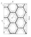
- FIG. 4 a is a top, plan view of the backplate 104 where the interconnect layer 200 c is formed to create posts 300 positioned between the holes 106 .
- the posts 300 can be solid.
- the posts 300 can be constructed as a ring wall that surrounds a core 302 (e.g., an oxide core).
- the core 302 can contain one or more materials or can be hollow.
- the posts 300 are illustrated in FIGS. 4 a and 4 b as being circular, it should be understood that the posts 300 can have any desired shape, such as triangular, square, polygonal, etc., and any size.
- the interconnect layer 200 c can be constructed as walls.
- FIG. 4 c is a top, plan view of the backplate 104 where the interconnect layer 200 c consists of a single continuous wall 304 between the holes 106 .
- the walls 304 are illustrated in FIG. 4 c as continuous straight walls, the walls 304 can be continuous or intermittent and straight or curved and can include one or more multiple walls (e.g., two parallel walls encapsulating a region between the walls that can be hollow or filled with one or more materials).
- FIG. 4 c
- 4 d is a top, plan view of the backplate 104 where the interconnect layer 200 c is constructed of multiple materials including one material used to form a plurality of continuous walls surrounding the backplate perimeter and each backplate opening in order to encapsulate and protect a second interconnect layer material in a region interior to the walls.
- FIGS. 5 a - c illustrate additional alternative constructions for the composite backplate 104 .
- FIG. 5 a illustrates a composite backplate 104 including an interconnect layer 200 c having a double wall 304 (see FIG. 4 c ) or discrete ring posts 300 (see FIGS. 4 a and 4 b ).
- the wall 304 or ring posts 300 protect a core 310 that can be filled with a different material than the interconnect layer 200 c , such as silicon dioxide.
- the core 310 can be hollow.
- An optional release hole 312 can be formed in the upper layer 200 a .
- the release hole 312 allows removal of material to create a core 310 that is hollow. It should be understood that the release hole 312 can alternatively or in addition be included in the lower layer 200 b.
- FIG. 5 b illustrates an alternative backplate 104 that includes an interconnect layer 200 c formed as either walls 304 or posts) where an upper portion of layer 200 c is wider or has a different shape than the lower portion.
- the upper portion of the layer 200 c matches a shape or size of the upper layer 200 a .
- Forming the interconnect layer 200 c in this fashion stiffens and provide more support to the upper layer 200 a .
- the constructions of the interconnect layer 200 c illustrated in FIG. 5 b can alternatively or in addition be used with the lower layer 200 b.
- a similar construction of the interconnect layer 200 c can also be used with no upper layer 200 a to form the backplate 104 (see FIG. 5 c ). As previously noted, forming the interconnect layer 200 c as illustrated in FIG. 5 c stiffens and provides support to the backplate 104 (e.g., the lower layer 200 b ). It should be understood that the constructions of the interconnect layer 200 c illustrated in FIG. 5 c can alternatively of in addition be used when the backplate 104 does not include a lower layer 200 b.
- embodiments of the invention provide, among other things, a composite backplate that is thin and highly perforated yet strong and flat with adequate tensile properties.
- the composite backplate can also provide better particle filtration with less reduction of acoustic signal-to-noise ratio than existing backplates.
- the same patterns can be used as a front plate in a MEMS system.
- the backplate (or frontplate) of this construction can be formed using CMOS MEMS material layers or traditional MEMS material layers and processing steps.
Landscapes
- Engineering & Computer Science (AREA)
- Physics & Mathematics (AREA)
- Acoustics & Sound (AREA)
- Signal Processing (AREA)
- Computer Hardware Design (AREA)
- Microelectronics & Electronic Packaging (AREA)
- Mechanical Engineering (AREA)
- Micromachines (AREA)
- Obtaining Desirable Characteristics In Audible-Bandwidth Transducers (AREA)
Abstract
Description
Claims (22)
Priority Applications (1)
| Application Number | Priority Date | Filing Date | Title |
|---|---|---|---|
| US14/894,390 US9648425B2 (en) | 2013-05-28 | 2014-05-28 | Multi-layer composite backplate for micromechanical microphone |
Applications Claiming Priority (3)
| Application Number | Priority Date | Filing Date | Title |
|---|---|---|---|
| US201361827982P | 2013-05-28 | 2013-05-28 | |
| PCT/US2014/039793 WO2014193954A1 (en) | 2013-05-28 | 2014-05-28 | Multi-layer composite backplate for micromechanical microphone |
| US14/894,390 US9648425B2 (en) | 2013-05-28 | 2014-05-28 | Multi-layer composite backplate for micromechanical microphone |
Related Parent Applications (1)
| Application Number | Title | Priority Date | Filing Date |
|---|---|---|---|
| PCT/US2014/039793 A-371-Of-International WO2014193954A1 (en) | 2013-05-28 | 2014-05-28 | Multi-layer composite backplate for micromechanical microphone |
Related Child Applications (1)
| Application Number | Title | Priority Date | Filing Date |
|---|---|---|---|
| US15/589,577 Continuation US20170245060A1 (en) | 2013-05-28 | 2017-05-08 | Multi-layer composite backplate for micromechanical microphone |
Publications (2)
| Publication Number | Publication Date |
|---|---|
| US20160127837A1 US20160127837A1 (en) | 2016-05-05 |
| US9648425B2 true US9648425B2 (en) | 2017-05-09 |
Family
ID=51022454
Family Applications (2)
| Application Number | Title | Priority Date | Filing Date |
|---|---|---|---|
| US14/894,390 Active US9648425B2 (en) | 2013-05-28 | 2014-05-28 | Multi-layer composite backplate for micromechanical microphone |
| US15/589,577 Abandoned US20170245060A1 (en) | 2013-05-28 | 2017-05-08 | Multi-layer composite backplate for micromechanical microphone |
Family Applications After (1)
| Application Number | Title | Priority Date | Filing Date |
|---|---|---|---|
| US15/589,577 Abandoned US20170245060A1 (en) | 2013-05-28 | 2017-05-08 | Multi-layer composite backplate for micromechanical microphone |
Country Status (4)
| Country | Link |
|---|---|
| US (2) | US9648425B2 (en) |
| EP (1) | EP3005729B1 (en) |
| CN (1) | CN105247890B (en) |
| WO (1) | WO2014193954A1 (en) |
Families Citing this family (3)
| Publication number | Priority date | Publication date | Assignee | Title |
|---|---|---|---|---|
| DE102016123130B4 (en) | 2016-11-30 | 2020-12-10 | Infineon Technologies Austria Ag | MEMS device and method of making a MEMS device |
| WO2018148871A1 (en) * | 2017-02-15 | 2018-08-23 | Harman International Industries, Incorporated | Air particle filter used in microphone |
| US20240340598A1 (en) * | 2023-04-07 | 2024-10-10 | Fortemedia, Inc. | Mems structure |
Citations (17)
| Publication number | Priority date | Publication date | Assignee | Title |
|---|---|---|---|---|
| US2868894A (en) * | 1955-09-14 | 1959-01-13 | Theodore J Schultz | Miniature condenser microphone |
| WO2006123299A2 (en) | 2005-05-18 | 2006-11-23 | Kolo Technologies, Inc. | Methods for fabricating micro-electro-mechanical devices |
| US20070264749A1 (en) * | 2006-05-15 | 2007-11-15 | Dimatix, Inc. | Multi-Post Structures |
| US20090122651A1 (en) | 2007-10-18 | 2009-05-14 | Mario Kupnik | Direct wafer bonded 2-D CUMT array |
| US20100119088A1 (en) * | 2007-04-25 | 2010-05-13 | University Of Florida Research Foundation, Inc. | Capacitive Microphone With Integrated Cavity |
| EP2202559A2 (en) * | 2004-09-27 | 2010-06-30 | Qualcomm Mems Technologies, Inc | Method and system for packaging a MEMS device |
| US20100164025A1 (en) | 2008-06-25 | 2010-07-01 | Yang Xiao Charles | Method and structure of monolithetically integrated micromachined microphone using ic foundry-compatiable processes |
| GB2467776A (en) * | 2009-02-13 | 2010-08-18 | Wolfson Microelectronics Plc | Integrated MEMS transducer and circuitry |
| CN202261791U (en) | 2011-09-13 | 2012-05-30 | 华景传感科技(无锡)有限公司 | MEMS (Micro Electro Mechanical System) silicon microphone longitudinally integrated with CMOS (Complementary Metal Oxide Semiconductor) circuit |
| US20120189143A1 (en) * | 2011-01-05 | 2012-07-26 | Robert Bosch Gmbh | Micromechanical Microphone Device and Method for Producing a Micromechanical Microphone Device |
| US20120225259A1 (en) | 2011-03-02 | 2012-09-06 | Epcos Ag | Flat back plate |
| EP2536168A2 (en) | 2011-06-15 | 2012-12-19 | Robert Bosch Gmbh | Epitaxial silicon CMOS-MEMS microphones and method for manufacturing |
| US20120319174A1 (en) | 2010-07-28 | 2012-12-20 | Goertek Inc. | Cmos compatible mems microphone and method for manufacturing the same |
| US20130285173A1 (en) * | 2012-04-27 | 2013-10-31 | Nxp B.V. | Acoustic transducers with perforated membranes |
| US8590136B2 (en) | 2009-08-28 | 2013-11-26 | Analog Devices, Inc. | Method of fabricating a dual single-crystal backplate microphone |
| US20130343580A1 (en) | 2012-06-07 | 2013-12-26 | Knowles Electronics, Llc | Back Plate Apparatus with Multiple Layers Having Non-Uniform Openings |
| US20140084396A1 (en) | 2012-09-24 | 2014-03-27 | Wolfson Microelectronics Plc. | Mems device and process |
Family Cites Families (5)
| Publication number | Priority date | Publication date | Assignee | Title |
|---|---|---|---|---|
| DE19509868A1 (en) * | 1995-03-17 | 1996-09-19 | Siemens Ag | Micromechanical semiconductor component |
| US8105941B2 (en) * | 2005-05-18 | 2012-01-31 | Kolo Technologies, Inc. | Through-wafer interconnection |
| US8447054B2 (en) * | 2009-11-11 | 2013-05-21 | Analog Devices, Inc. | Microphone with variable low frequency cutoff |
| US9245834B2 (en) * | 2012-03-16 | 2016-01-26 | Stats Chippac, Ltd. | Semiconductor device and method of forming compliant conductive interconnect structure in flipchip package |
| US8921956B2 (en) * | 2013-01-25 | 2014-12-30 | Infineon Technologies Ag | MEMS device having a back plate with elongated protrusions |
-
2014
- 2014-05-28 US US14/894,390 patent/US9648425B2/en active Active
- 2014-05-28 EP EP14733451.0A patent/EP3005729B1/en active Active
- 2014-05-28 WO PCT/US2014/039793 patent/WO2014193954A1/en not_active Ceased
- 2014-05-28 CN CN201480030794.4A patent/CN105247890B/en active Active
-
2017
- 2017-05-08 US US15/589,577 patent/US20170245060A1/en not_active Abandoned
Patent Citations (17)
| Publication number | Priority date | Publication date | Assignee | Title |
|---|---|---|---|---|
| US2868894A (en) * | 1955-09-14 | 1959-01-13 | Theodore J Schultz | Miniature condenser microphone |
| EP2202559A2 (en) * | 2004-09-27 | 2010-06-30 | Qualcomm Mems Technologies, Inc | Method and system for packaging a MEMS device |
| WO2006123299A2 (en) | 2005-05-18 | 2006-11-23 | Kolo Technologies, Inc. | Methods for fabricating micro-electro-mechanical devices |
| US20070264749A1 (en) * | 2006-05-15 | 2007-11-15 | Dimatix, Inc. | Multi-Post Structures |
| US20100119088A1 (en) * | 2007-04-25 | 2010-05-13 | University Of Florida Research Foundation, Inc. | Capacitive Microphone With Integrated Cavity |
| US20090122651A1 (en) | 2007-10-18 | 2009-05-14 | Mario Kupnik | Direct wafer bonded 2-D CUMT array |
| US20100164025A1 (en) | 2008-06-25 | 2010-07-01 | Yang Xiao Charles | Method and structure of monolithetically integrated micromachined microphone using ic foundry-compatiable processes |
| GB2467776A (en) * | 2009-02-13 | 2010-08-18 | Wolfson Microelectronics Plc | Integrated MEMS transducer and circuitry |
| US8590136B2 (en) | 2009-08-28 | 2013-11-26 | Analog Devices, Inc. | Method of fabricating a dual single-crystal backplate microphone |
| US20120319174A1 (en) | 2010-07-28 | 2012-12-20 | Goertek Inc. | Cmos compatible mems microphone and method for manufacturing the same |
| US20120189143A1 (en) * | 2011-01-05 | 2012-07-26 | Robert Bosch Gmbh | Micromechanical Microphone Device and Method for Producing a Micromechanical Microphone Device |
| US20120225259A1 (en) | 2011-03-02 | 2012-09-06 | Epcos Ag | Flat back plate |
| EP2536168A2 (en) | 2011-06-15 | 2012-12-19 | Robert Bosch Gmbh | Epitaxial silicon CMOS-MEMS microphones and method for manufacturing |
| CN202261791U (en) | 2011-09-13 | 2012-05-30 | 华景传感科技(无锡)有限公司 | MEMS (Micro Electro Mechanical System) silicon microphone longitudinally integrated with CMOS (Complementary Metal Oxide Semiconductor) circuit |
| US20130285173A1 (en) * | 2012-04-27 | 2013-10-31 | Nxp B.V. | Acoustic transducers with perforated membranes |
| US20130343580A1 (en) | 2012-06-07 | 2013-12-26 | Knowles Electronics, Llc | Back Plate Apparatus with Multiple Layers Having Non-Uniform Openings |
| US20140084396A1 (en) | 2012-09-24 | 2014-03-27 | Wolfson Microelectronics Plc. | Mems device and process |
Non-Patent Citations (1)
| Title |
|---|
| International Search Report and Written Opinion for Application No. PCT/US2014/039793 dated Jun. 2, 2014, 9 pages. |
Also Published As
| Publication number | Publication date |
|---|---|
| CN105247890A (en) | 2016-01-13 |
| EP3005729A1 (en) | 2016-04-13 |
| EP3005729B1 (en) | 2020-08-05 |
| US20160127837A1 (en) | 2016-05-05 |
| WO2014193954A1 (en) | 2014-12-04 |
| US20170245060A1 (en) | 2017-08-24 |
| CN105247890B (en) | 2019-03-29 |
Similar Documents
| Publication | Publication Date | Title |
|---|---|---|
| KR102381099B1 (en) | System and method for a mems transducer | |
| EP3005730B1 (en) | Mesh in mesh backplate for micromechanical microphone | |
| KR101740113B1 (en) | A mems sensor structure for sensing pressure waves and a change in ambient pressure | |
| CN106688245B (en) | MEMS speaker with actuator structure and diaphragm spaced therefrom | |
| US20180048951A1 (en) | Package structure of mems microphone | |
| CN102066239A (en) | MEMS device | |
| ITUA20163571A1 (en) | MEMS ACOUSTIC TRANSDUCER WITH INTERDIGATED ELECTRODES AND ITS MANUFACTURING PROCEDURE | |
| US20170245060A1 (en) | Multi-layer composite backplate for micromechanical microphone | |
| WO2008103672B1 (en) | Microfabricated microphone | |
| KR20140121623A (en) | Mems microphone having multiple sound pass hole | |
| US9232318B2 (en) | Hearing device with a microphone | |
| CN105144750B (en) | sound changer | |
| EP3243337B1 (en) | Microphone with dustproof through holes | |
| ITTO20130441A1 (en) | DETECTION STRUCTURE FOR A MEMS ACOUSTIC TRANSDUCER WITH IMPROVED DEFORMATION RESISTANCE | |
| US10623852B2 (en) | MEMS devices and processes | |
| WO2014045042A1 (en) | Mems device and process | |
| US20160112803A1 (en) | Mems microphone element | |
| US20180132023A1 (en) | Microphone and manufacturing method thereof | |
| CN104270701A (en) | Vibrating diaphragm structure of MEMS microphone and manufacturing method thereof | |
| US20240171917A1 (en) | Electrodes for microelectromechanical system microphones | |
| WO2024112406A1 (en) | Electrodes for microelectromechanical system microphones | |
| TWI473506B (en) | Member with micro mechanical microphone structure and manufacturing method thereof | |
| CN204119483U (en) | Diaphragm structure in a kind of MEMS microphone | |
| KR20190044905A (en) | Capcitive microphone | |
| KR102409521B1 (en) | Mems microphone |
Legal Events
| Date | Code | Title | Description |
|---|---|---|---|
| AS | Assignment |
Owner name: ROBERT BOSCH GMBH, GERMANY Free format text: ASSIGNMENT OF ASSIGNORS INTEREST;ASSIGNORS:ZINN, JOHN W.;DIAMOND, BRETT MATHEW;REEL/FRAME:037940/0759 Effective date: 20130930 Owner name: AKUSTICA, INC., PENNSYLVANIA Free format text: ASSIGNMENT OF ASSIGNORS INTEREST;ASSIGNORS:ZINN, JOHN W.;DIAMOND, BRETT MATHEW;REEL/FRAME:037940/0759 Effective date: 20130930 |
|
| STCF | Information on status: patent grant |
Free format text: PATENTED CASE |
|
| MAFP | Maintenance fee payment |
Free format text: PAYMENT OF MAINTENANCE FEE, 4TH YEAR, LARGE ENTITY (ORIGINAL EVENT CODE: M1551); ENTITY STATUS OF PATENT OWNER: LARGE ENTITY Year of fee payment: 4 |
|
| MAFP | Maintenance fee payment |
Free format text: PAYMENT OF MAINTENANCE FEE, 8TH YEAR, LARGE ENTITY (ORIGINAL EVENT CODE: M1552); ENTITY STATUS OF PATENT OWNER: LARGE ENTITY Year of fee payment: 8 |