US9645963B2 - Systems and methods for concurrently testing master and slave devices in a system on a chip - Google Patents
Systems and methods for concurrently testing master and slave devices in a system on a chip Download PDFInfo
- Publication number
- US9645963B2 US9645963B2 US14/623,293 US201514623293A US9645963B2 US 9645963 B2 US9645963 B2 US 9645963B2 US 201514623293 A US201514623293 A US 201514623293A US 9645963 B2 US9645963 B2 US 9645963B2
- Authority
- US
- United States
- Prior art keywords
- slave
- master
- test
- clock signal
- coupled
- Prior art date
- Legal status (The legal status is an assumption and is not a legal conclusion. Google has not performed a legal analysis and makes no representation as to the accuracy of the status listed.)
- Active, expires
Links
Images


Classifications
-
- G—PHYSICS
- G06—COMPUTING OR CALCULATING; COUNTING
- G06F—ELECTRIC DIGITAL DATA PROCESSING
- G06F13/00—Interconnection of, or transfer of information or other signals between, memories, input/output devices or central processing units
- G06F13/38—Information transfer, e.g. on bus
- G06F13/40—Bus structure
- G06F13/4063—Device-to-bus coupling
- G06F13/4068—Electrical coupling
-
- G—PHYSICS
- G01—MEASURING; TESTING
- G01R—MEASURING ELECTRIC VARIABLES; MEASURING MAGNETIC VARIABLES
- G01R31/00—Arrangements for testing electric properties; Arrangements for locating electric faults; Arrangements for electrical testing characterised by what is being tested not provided for elsewhere
- G01R31/28—Testing of electronic circuits, e.g. by signal tracer
- G01R31/317—Testing of digital circuits
- G01R31/31707—Test strategies
-
- G—PHYSICS
- G01—MEASURING; TESTING
- G01R—MEASURING ELECTRIC VARIABLES; MEASURING MAGNETIC VARIABLES
- G01R31/00—Arrangements for testing electric properties; Arrangements for locating electric faults; Arrangements for electrical testing characterised by what is being tested not provided for elsewhere
- G01R31/28—Testing of electronic circuits, e.g. by signal tracer
- G01R31/317—Testing of digital circuits
- G01R31/31727—Clock circuits aspects, e.g. test clock circuit details, timing aspects for signal generation, circuits for testing clocks
Definitions
- This disclosure relates generally to testing systems on a chip with master and slave devices, and more specifically, to concurrently testing master and slave devices in a system on a chip.
- SoC System on a Chip
- MCU microcontroller unit
- FIG. 1 is a block diagram of an embodiment of a test system for integrated circuitry in accordance with the present invention.
- FIG. 2 is a block diagram of another embodiment of integrated circuitry in accordance with the present invention.
- FIG. 3 is a flow diagram showing an example of concurrent testing of master and slave systems on the integrated circuitry of FIGS. 1 and 2 .
- Embodiments of systems and methods are disclosed that allow a slave system to be tested in parallel with a master system in an integrated circuit device.
- the master system configures the slave system for a test.
- the slave system is then isolated from the master system by blocking reset signals to the slave system and signals such as interrupts from the slave system to the master system.
- a separate clock signal can also be used in the slave system independent of the clock signal used by the master system during the testing.
- the master system can perform its own test(s), including testing built-in flash memory.
- the master and slave systems can be tested repeatedly as required, per normal test requirements. After both systems have completed their individual testing, the isolation can be removed and any interdependent tests can be performed.
- the master system is typically a microcontroller and the slave system can be any other suitable device such as a radio system, another microcontroller, or a radio with a built-in microcontroller.
- the SoC can also include more than one slave device, and all the slave devices can be tested in parallel with one another and with the master system.
- FIG. 1 is a block diagram of an embodiment of a test system 100 including a substrate with integrated circuitry 102 for a System on a Chip (SoC) that can communicate with SoC test resources 104 and radio test resources 106 .
- SoC System on a Chip
- Implemented on substrate is a master system in the form of microcontroller unit (MCU) 108 and a slave system in the form of radio system 112 .
- MCU microcontroller unit
- Either an internal clock or an external clock will provide a clock signal to clock select logic 124 in radio system 112 via I/O pads or pins 114 , 116 .
- a test or master clock signal can also be provided to clock select logic 124 .
- clock select logic 124 can use a high quality clock signal from the internal clock or external clock while MCU 108 uses a master clock or other clock signal that does not require the same level of quality as the clock signal for testing radio system 112 . During normal operation, clock select logic 124 can provide the master system clock to radio system 112 .
- Reset isolation indicator 120 and radio isolation indicator 122 can be included in radio system 112 to isolate radio system 112 from MCU 108 during test periods.
- Reset isolation indicator 120 and radio isolation indicator 122 are set by MCU 108 after radio system 112 is configured for a test.
- Reset isolation indicator 120 is coupled to an inverting input of logic gate 128 and a SoC reset signal is coupled to a non-inverting input of logic gate 128 .
- the output of logic gate 128 will provide a reset signal to radio system 112 when the reset isolation indicator is set low, but will block the reset signal otherwise.
- Radio isolation indicator 122 is coupled to an inverting input of logic gate 130 and radio signals such as interrupts from radio system 112 are coupled to a non-inverting input of logic gate 130 .
- the output of logic gate 130 will provide interrupt signals to MCU 108 when the radio isolation indicator is set low, but will block the interrupt signals otherwise.
- the reset isolation indicator and radio isolation indicators are set high during test periods in the embodiment shown.
- Logic gates 128 , 130 are shown as AND gates, but can be implemented using other suitable logic gates in combination with inputs configured to isolate radio system 112 from receiving reset signals and sending interrupt signals to MCU 108 .
- MCU 108 and logic gate 128 can receive the reset signal via Input/Output (I/O) pad 132 formed at the perimeter or other suitable location on substrate or in the SoC.
- I/O pads 134 can also be included to provide a system or master clock signal to MCU 108 , along with conducting other signals being communicated to and from MCU 108 .
- RF radio frequency
- SoC test resources 104 can be coupled to reset pad 132 and I/O pads 134 , and is configured to provide configuration set-up information and test inputs to MCU 108 .
- the tests can be designed to check functionality of processing cores, memory devices, serial and parallel I/O, timers, system integration and other functions of MCU 108 .
- Configuration information for testing one or more slave systems can be provided by SoC test resources and distributed by MCU 108 to the slave systems. For example, when the slave system is a radio system 112 , MCU 108 can provide test configuration information to test RF control, RF analog inputs, RF link layer, RF registers, system integration, and other functionality of radio system 112 .
- Radio test resources 106 can be coupled to RF I/O pads 126 to provide test configuration information to radio system 112 in addition to or instead of information being provided by MCU 108 to radio system 112 .
- corresponding test resources may be included instead of radio test resources 106 .
- logic to provide configuration information and to set the reset and radio isolation indicators may be implemented in software, hardware, or any combination thereof.
- FIG. 2 is a block diagram of another embodiment of an SoC test configuration, where the radio system MCU 220 can perform testing using a clean clock signal from an RF crystal oscillator clock source fed via I/O pads or pins 214 and 216 , an external single-ended clock in parallel with MCU 208 that uses a separate test clock 234 or a master clock generated on the integrated circuit 202 .
- Signals provided on pins 214 , 216 can be used in a differential manner to attach an RF crystal oscillator for the combination radio system 212 and MCU 220 .
- the external crystal works with an on-chip reference oscillator circuit that is used to condition the sinusoidal oscillation waveform from the crystal reference to a buffered and amplitude scaled square wave.
- This clock is then used as the reference clock in radio system 212 .
- the buffered and conditioned output from this external reference can be provided in a single-ended fashion to radio system 212 via pin 216 .
- this single-ended input can also be used on a test platform to inject a tester based high purity clock to the radio, which is also available to the external test resources to allow for synchronized operations between the external tester and radio platform under test.
- Integrated circuit or SoC 202 includes a substrate that can communicate with SoC test resources 104 and radio test resources 106 of FIG. 1 .
- SoC 202 includes a master system in the form of microcontroller unit (MCU) 208 and a slave system in the form of radio system 212 .
- MCU microcontroller unit
- Either an internal clock or external clock signal will provide a clock signal to clock select logic 224 in radio system 212 via pins 214 , 216 .
- a test or master clock signal can also be provided to clock select logic 224 .
- clock select logic 224 can use a high quality clock signal from an external RF (crystal) Oscillator clock or an external single-ended clock while MCU 208 uses a master clock or other clock signal that does not require the same level of quality as the clock signal for testing radio system 212 .
- clock select logic 224 can provide the master system clock to radio system 212 .
- MCU 208 can receive a system or master reset signal via Input/Output (I/O) pad 232 formed at the perimeter or other suitable location on or in the SoC.
- I/O pads 234 can also be included to provide a test or master clock signal to MCU 208 , along with conducting other signals being communicated to and from MCU 208 and radio system 212 .
- radio system 212 can receive an auxiliary reset signal via one or I/O pads 234 .
- the auxiliary reset signal can be generated by a controller external to SoC 202 and is independent of the master reset signal that is sent to MCU 208 and can be used by MCU 220 and/or by other components in radio system 212 during test periods.
- RF radio frequency
- SoC 202 can also include a shared memory device 230 that is coupled to MCU 208 and radio system 212 .
- Memory device 230 can be used to communicate test configuration parameters and other information between MCU 208 and radio system 212 .
- one or more isolation indicators can be used during test periods to prevent reset signals from MCU 208 being sent to radio system 212 , and to further prevent interrupts and other signals being sent from radio system 212 to MCU 208 during test periods.
- Test resources 204 can be coupled to one or more debug interface pads 236 on SoC 202 to gain independent access to registers 222 in radio system 212 .
- Test resources 204 can provide test configuration parameters, clock select, and isolation indicators in addition to or instead of the test configuration parameters, clock select, and isolation indicators from MCU 208 via a suitable debug interface such as Single Wire Debug (SWD) or Joint Test Action Group (JTAG) debug interfaces.
- SWD Single Wire Debug
- JTAG Joint Test Action Group
- Test resources 204 can also be coupled to reset pad 232 and I/O pads 234 to provide configuration set-up information and test inputs to MCU 208 .
- the tests can be designed to check functionality of processing cores, memory devices, serial and parallel I/O, timers, system integration and other functions of MCU 208 .
- Configuration information for testing one or more slave systems can be provided by SoC test resources 204 and distributed by MCU 208 to the slave system(s). For example, when the slave system is radio system 212 , MCU 208 can provide test configuration information to test MCU 220 , RF control, RF analog inputs, RF link layer, RF registers, system integration, and other functionality of radio system 212 .
- Test resources 204 can also be coupled to RF I/O pads 226 to provide test configuration information to radio system 212 in addition to or instead of information being provided by MCU 208 to radio system 212 or via debug interfaces 236 .
- the slave system is another type of device other than radio system 212
- other appropriate test resources may be included instead of test resources 204 .
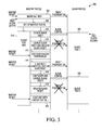
- FIG. 3 is a flow diagram showing an example of a method 300 to concurrently test master and slave systems in the integrated circuitry 100 , 200 of FIGS. 1 and 2 .
- Process 302 begins the SoC test by receiving a reset signal in the master system.
- the master system can propagate the reset signal to the slave system.
- the reset signal may originate in a controller for a device that uses the SoC.
- a system clock signal is also received in the master system, typically at regular intervals.
- Process 306 can include setting test parameters for the master device including any and all components in the master device such as flash memory, processor core(s), I/O interfaces, system integration, and timers in the master system, among others.
- Process 308 includes configuring test parameters for the slave system in the master system, and sending the test parameters from the master system to the slave system.
- the parameters can include an indicator of whether the slave system should use the master clock signal or another clock signal that is more accurate, among other parameters and indicators.
- test configuration information can be provided to the slave system from external test resources via a debug interface.
- Process 310 can include isolating the master system from the slave system and launching the test in the slave system, as indicated by process 330 .
- a reset isolation indicator and a radio (or slave) isolation indicator can be set to prevent system reset signals from being propagated from the master system to the slave system, and to further prevent interrupt signals from being propagated from the slave system to the master system during the test period(s).
- a reset signal from the master system to the slave system is shown crossed out during the first test of the slave system in FIG. 3 to indicate that the reset signal is prevented from being received in the slave system.
- logic can be included in the slave system to ignore reset signals in the slave system based on the reset isolation indicator.
- Process 311 can include starting the test of any components that require a significant amount of time to test, such as flash memory, at the start of the test period in the master system once the test for the master system has been configured.
- Process 312 can include testing other components in the master system concurrently with the test of flash memory in the master system and with the test being performed in the slave system.
- process 314 includes sending a reset signal from the master system to the slave system.
- the reset isolation in the slave system can be disabled to allow the reset signal to be sent from the master system to the slave system. Note that the interrupt isolation can remain enabled while the slave system is reset to prevent the slave system from affecting the test(s) being conducted concurrently in the master system.
- Process 316 can include the master system configuring a second test for the slave system if more than one test is to be performed on the slave system.
- the second test configuration is then provided to the slave system from the master system.
- test configuration information can be provided to the slave system from external test resources via a debug interface.
- process 318 re-establishes reset isolation between the master and slave systems, and the second test of the slave system can be initiated and performed concurrently with tests running in the master system, as indicated by process 332 .
- a reset signal from the master system to the slave system is shown crossed out during the second test of the slave system in FIG. 3 to indicate that the reset signal is prevented from being received in the slave system.
- logic can be included in the slave system to ignore reset signals in the slave system based on the reset isolation indicator.
- Process 320 includes continuing to test components in the master system while the second test is performed in the slave system. Note that as many tests as desired can be performed in the master and slave systems. Additionally, two or more tests can run concurrently in either or both of the slave system and the master system. Further, the master system can configure tests for more than one slave system, and the additional slave systems can also be isolated from the master system during the test periods.
- an integrated circuit that can include a substrate, a master system ( 108 ) on the substrate, a slave system ( 112 ) on the substrate and coupled to communicate with the master system, a first clock signal coupled to the master system, and a second clock signal coupled to the slave system.
- the master system is configured to isolate the slave system from the master system while a first test of the master system is conducted in parallel with a second test of the slave system.
- the master system uses the first clock signal during the first test and the slave system uses the second clock signal during the second test.
- the master system can isolate the slave system by blocking a reset signal to the slave system during the second test.
- the slave system can include clock select logic configured to choose between a test clock signal from the master system and the second clock signal.
- the IC can further comprise a memory device on the substrate coupled to communicate with the master and slave systems during the first and second test.
- the IC can further comprise a first set of input/output pads on the substrate and coupled only to the master system, and a second set of input/output pads on the substrate and coupled only to the slave system.
- the IC can further comprise a debug input/output pad on the substrate coupled to a register in the slave system, wherein the debug input/output pad is used to input a signal to isolate the slave system from the master system.
- the master system can be a microcontroller and the slave system can be a radio system.
- the radio system can include a second microcontroller.
- the master and the slave systems can be microcontrollers.
- the IC can further comprise a master reset signal coupled to the master system, and an auxiliary reset signal coupled to the slave system.
- the auxiliary reset signal can be enabled only during the second test.
- the auxiliary reset signal can be used by a second microcontroller in the slave system.
- the IC can further comprise a first logic gate configured to block a reset signal to the slave system when reset blocking is enabled.
- the IC can further comprise a second logic gate configured to block interrupt signals from the slave system to the master system when slave output blocking is enabled.
- a method of testing an integrated circuit device can comprise isolating a slave device from a master device by blocking a reset signal to the slave device during a test period, providing a first clock signal to the master device, providing a second clock signal to the slave device during the test period, testing the slave device in parallel with testing the master device during the test period, and using the first clock signal to operate the slave device and the master device during normal operation.
- the method can further comprise sharing a memory device between the master device and the slave device during the test period.
- the method can further comprise blocking interrupt signals from the slave system to the master system when slave output blocking is enabled.
- the master system can be a microcontroller and the slave system can be at least one of a group consisting of a radio system and a second microcontroller.
- the method can further comprise configuring the slave system for the test period before blocking the reset signal.
- the method can further comprise utilizing an auxiliary reset signal for the slave device during the test period.
- isolating the slave system from the master system can include using a debug input/output pad to provide a signal to indicate whether to block the reset signal.
- the systems and methods disclosed herein may be incorporated into a wide range of electronic devices including, for example, computer systems or Information Technology (IT) products (e.g., servers, desktops, laptops, switches, routers, etc.), telecommunications hardware, consumer devices or appliances (e.g., mobile phones, tablets, televisions, cameras, sound systems, etc.), scientific instrumentation, industrial robotics, medical or laboratory electronics (e.g., imaging, diagnostic, or therapeutic equipment, etc.), transportation vehicles (e.g., automobiles, buses, trains, watercraft, aircraft, etc.), military equipment, etc. More generally, the systems and methods discussed herein may be incorporated into any device or system having one or more electronic parts or components.
- IT Information Technology
- Examples of integrated circuitry 102 may include, for instance, a System-On-Chip (SoC), an Application Specific Integrated Circuit (ASIC), a Digital Signal Processor (DSP), a Field-Programmable Gate Array (FPGA), a processor, a microprocessor, a controller, a microcontroller (MCU), or the like.
- SoC System-On-Chip
- ASIC Application Specific Integrated Circuit
- DSP Digital Signal Processor
- FPGA Field-Programmable Gate Array
- processor a microprocessor
- controller a microcontroller
- integrated circuit(s) 102 may include a memory circuit or device such as, for example, a Random Access Memory (RAM), a Static RAM (SRAM), a Magnetoresistive RAM (MRAM), a Nonvolatile RAM (NVRAM, such as “FLASH” memory, etc.), and/or a Dynamic RAM (DRAM) such as Synchronous DRAM (SDRAM), a Double Data Rate (e.g., DDR, DDR2, DDR3, etc.) RAM, an Erasable Programmable ROM (EPROM), an Electrically Erasable Programmable ROM (EEPROM), etc.
- RAM Random Access Memory
- SRAM Static RAM
- MRAM Magnetoresistive RAM
- NVRAM Nonvolatile RAM
- DRAM Dynamic RAM
- SDRAM Synchronous DRAM
- EPROM Erasable Programmable ROM
- EEPROM Electrically Erasable Programmable ROM
- integrated circuitry 102 may include one or more mixed-signal or analog circuits, such as, for example, Analog-to-Digital Converter (ADCs), Digital-to-Analog Converter (DACs), Phased Locked Loop (PLLs), oscillators, filters, amplifiers, transformers, etc. Additionally or alternatively, integrated circuit(s) 102 may include one or more Micro-ElectroMechanical Systems (MEMS), Nano-ElectroMechanical Systems (NEMS), or the like.
- ADCs Analog-to-Digital Converter
- DACs Digital-to-Analog Converter
- PLLs Phased Locked Loop
- integrated circuit(s) 102 may include one or more Micro-ElectroMechanical Systems (MEMS), Nano-ElectroMechanical Systems (NEMS), or the like.
- MEMS Micro-ElectroMechanical Systems
- NEMS Nano-ElectroMechanical Systems
- integrated circuitry 102 may include a number of different portions, areas, or regions. These various portions may include one or more processing cores, cache memories, internal bus(es), timing units, controllers, analog sections, mechanical elements, etc.
- integrated circuit(s) 102 may include a bandgap circuit and a trimming circuit configured to set or control an output voltage—that is, a bandgap voltage—provided by the bandgap circuit. During the production test of integrated circuit(s) 102 , the trimming circuit may be adjusted using the various systems and methods for trimming acceleration described herein.
- Integrated circuit(s) 102 may be disposed within an electronic component package configured to be mounted onto printed circuit board (PCB) using any suitable packaging technology such as, for example, Ball Grid Array (BGA) packaging or the like.
- PCB printed circuit board
- BGA Ball Grid Array
- the PCB may be mechanically mounted within or fastened onto an electronic device.
- FIG. 1 and the discussion thereof describe an exemplary information processing architecture
- this exemplary architecture is presented merely to provide a useful reference in discussing various aspects of the disclosure.
- the description of the architecture has been simplified for purposes of discussion, and it is just one of many different types of appropriate architectures that may be used in accordance with the disclosure.
- Those skilled in the art will recognize that the boundaries between logic blocks are merely illustrative and that alternative embodiments may merge logic blocks or circuit elements or impose an alternate decomposition of functionality upon various logic blocks or circuit elements.
- any two components herein combined to achieve a particular functionality can be seen as “associated with” each other such that the desired functionality is achieved, irrespective of architectures or intermedial components.
- any two components so associated can also be viewed as being “operably connected,” or “operably coupled,” to each other to achieve the desired functionality.
Landscapes
- Engineering & Computer Science (AREA)
- General Engineering & Computer Science (AREA)
- Physics & Mathematics (AREA)
- General Physics & Mathematics (AREA)
- Theoretical Computer Science (AREA)
- Computer Hardware Design (AREA)
- Semiconductor Integrated Circuits (AREA)
Abstract
Description
Claims (19)
Priority Applications (1)
| Application Number | Priority Date | Filing Date | Title |
|---|---|---|---|
| US14/623,293 US9645963B2 (en) | 2015-02-16 | 2015-02-16 | Systems and methods for concurrently testing master and slave devices in a system on a chip |
Applications Claiming Priority (1)
| Application Number | Priority Date | Filing Date | Title |
|---|---|---|---|
| US14/623,293 US9645963B2 (en) | 2015-02-16 | 2015-02-16 | Systems and methods for concurrently testing master and slave devices in a system on a chip |
Publications (2)
| Publication Number | Publication Date |
|---|---|
| US20160238654A1 US20160238654A1 (en) | 2016-08-18 |
| US9645963B2 true US9645963B2 (en) | 2017-05-09 |
Family
ID=56622087
Family Applications (1)
| Application Number | Title | Priority Date | Filing Date |
|---|---|---|---|
| US14/623,293 Active 2035-05-15 US9645963B2 (en) | 2015-02-16 | 2015-02-16 | Systems and methods for concurrently testing master and slave devices in a system on a chip |
Country Status (1)
| Country | Link |
|---|---|
| US (1) | US9645963B2 (en) |
Families Citing this family (2)
| Publication number | Priority date | Publication date | Assignee | Title |
|---|---|---|---|---|
| US20190242941A1 (en) * | 2018-02-06 | 2019-08-08 | Marvell World Trade Ltd. | Methods and Apparatus for Testing an Integrated Circuit |
| FR3089322B1 (en) * | 2018-11-29 | 2020-12-18 | St Microelectronics Rousset | Managing access restrictions within a system on a chip |
Citations (13)
| Publication number | Priority date | Publication date | Assignee | Title |
|---|---|---|---|---|
| US5187794A (en) * | 1989-03-15 | 1993-02-16 | The United States Of America As Represented By The Administrator Of The National Aeronautics And Space Administration | System for simultaneously loading program to master computer memory devices and corresponding slave computer memory devices |
| US5392297A (en) | 1989-04-18 | 1995-02-21 | Vlsi Technology, Inc. | Method for automatic isolation of functional blocks within integrated circuits |
| US6000051A (en) * | 1997-10-10 | 1999-12-07 | Logic Vision, Inc. | Method and apparatus for high-speed interconnect testing |
| US6076177A (en) | 1997-09-23 | 2000-06-13 | Motorola, Inc. | Method and apparatus for testing a circuit module concurrently with a non-volatile memory operation in a multi-module data processing system |
| US6925408B2 (en) | 2003-09-08 | 2005-08-02 | Texas Instruments Incorporated | Mixed-signal core design for concurrent testing of mixed-signal, analog, and digital components |
| US7225285B1 (en) * | 2004-09-07 | 2007-05-29 | Altera Corporation | Assigning interrupts in multi-master systems |
| US20090158107A1 (en) * | 2007-12-12 | 2009-06-18 | Infineon Technologies Ag | System-on-chip with master/slave debug interface |
| US20100032669A1 (en) | 2008-08-08 | 2010-02-11 | Sun Mo An | Semiconductor integrated circuit capable of controlling test modes without stopping test |
| US8122306B2 (en) | 2007-06-26 | 2012-02-21 | Hynix Semiconductor Inc. | Test circuit for supporting concurrent test mode in a semiconductor memory |
| US8330477B1 (en) | 2008-01-17 | 2012-12-11 | Marvell International Ltd. | Test engine for integrated circuit chip testing |
| US20130162274A1 (en) | 2011-12-21 | 2013-06-27 | Hong-Sok Choi | Semiconductor integrated circuit and test control method thereof |
| US20140122756A1 (en) * | 2012-10-30 | 2014-05-01 | Anayas360.Com, Llc | Address based serial communication interface for control and monitoring of system-on-chip implementations |
| US20140351359A1 (en) * | 2013-05-24 | 2014-11-27 | Arm Limited | Data processing apparatus and method for communicating between a master device and an asychronous slave device via an interface |
-
2015
- 2015-02-16 US US14/623,293 patent/US9645963B2/en active Active
Patent Citations (13)
| Publication number | Priority date | Publication date | Assignee | Title |
|---|---|---|---|---|
| US5187794A (en) * | 1989-03-15 | 1993-02-16 | The United States Of America As Represented By The Administrator Of The National Aeronautics And Space Administration | System for simultaneously loading program to master computer memory devices and corresponding slave computer memory devices |
| US5392297A (en) | 1989-04-18 | 1995-02-21 | Vlsi Technology, Inc. | Method for automatic isolation of functional blocks within integrated circuits |
| US6076177A (en) | 1997-09-23 | 2000-06-13 | Motorola, Inc. | Method and apparatus for testing a circuit module concurrently with a non-volatile memory operation in a multi-module data processing system |
| US6000051A (en) * | 1997-10-10 | 1999-12-07 | Logic Vision, Inc. | Method and apparatus for high-speed interconnect testing |
| US6925408B2 (en) | 2003-09-08 | 2005-08-02 | Texas Instruments Incorporated | Mixed-signal core design for concurrent testing of mixed-signal, analog, and digital components |
| US7225285B1 (en) * | 2004-09-07 | 2007-05-29 | Altera Corporation | Assigning interrupts in multi-master systems |
| US8122306B2 (en) | 2007-06-26 | 2012-02-21 | Hynix Semiconductor Inc. | Test circuit for supporting concurrent test mode in a semiconductor memory |
| US20090158107A1 (en) * | 2007-12-12 | 2009-06-18 | Infineon Technologies Ag | System-on-chip with master/slave debug interface |
| US8330477B1 (en) | 2008-01-17 | 2012-12-11 | Marvell International Ltd. | Test engine for integrated circuit chip testing |
| US20100032669A1 (en) | 2008-08-08 | 2010-02-11 | Sun Mo An | Semiconductor integrated circuit capable of controlling test modes without stopping test |
| US20130162274A1 (en) | 2011-12-21 | 2013-06-27 | Hong-Sok Choi | Semiconductor integrated circuit and test control method thereof |
| US20140122756A1 (en) * | 2012-10-30 | 2014-05-01 | Anayas360.Com, Llc | Address based serial communication interface for control and monitoring of system-on-chip implementations |
| US20140351359A1 (en) * | 2013-05-24 | 2014-11-27 | Arm Limited | Data processing apparatus and method for communicating between a master device and an asychronous slave device via an interface |
Non-Patent Citations (1)
| Title |
|---|
| Q. Xu et al., Wrapper design for testing IP cores with multiple clock domains, in Proc. Design, Automation and Test in Europe Conf., pp. 416-421, Feb. 2004. * |
Also Published As
| Publication number | Publication date |
|---|---|
| US20160238654A1 (en) | 2016-08-18 |
Similar Documents
| Publication | Publication Date | Title |
|---|---|---|
| US9547043B2 (en) | Test control point insertion and X-bounding for logic built-in self-test (LBIST) using observation circuitry | |
| US8805636B2 (en) | Protocol aware digital channel apparatus | |
| US8461865B2 (en) | Logic built-in self-test system and method for applying a logic built-in self-test to a device under test | |
| US5721740A (en) | Flip-flop controller for selectively disabling clock signal | |
| US9583216B2 (en) | MBIST device for use with ECC-protected memories | |
| JP6594309B2 (en) | Channel circuit and automatic test system | |
| US8901991B2 (en) | Power monitoring circuitry | |
| US9429630B2 (en) | Circuit for testing power supplies in multiple power modes | |
| US9595350B2 (en) | Hardware-based memory initialization | |
| US9645963B2 (en) | Systems and methods for concurrently testing master and slave devices in a system on a chip | |
| US9366725B1 (en) | Multiplexer circuit | |
| US20150046763A1 (en) | Apparatus and Method for Controlling Internal Test Controllers | |
| US20170366177A1 (en) | Integrated circuit and method of testing | |
| US20150178102A1 (en) | System-on-chip, method of manufacture thereof and method of controlling a system-on-chip | |
| US6085343A (en) | Method for concurrent testing of on-chip circuitry and timing counters | |
| US9234942B2 (en) | Transition fault testing of source synchronous interface | |
| US20150035561A1 (en) | Apparatus and method for correcting output signal of fpga-based memory test device | |
| US11715544B2 (en) | System and method for low power memory test | |
| US8793545B2 (en) | Apparatus and method for clock glitch detection during at-speed testing | |
| US8773180B2 (en) | Device for generating reset signal having sufficient pulse width | |
| CN106199256A (en) | The method for designing of TCXO test circuit | |
| JP2007155670A (en) | Power source noise resistance inspection circuit, and power source noise resistance inspection method | |
| JP6304472B2 (en) | Semiconductor integrated circuit, oscillator, electronic device, moving object, and method for inspecting semiconductor integrated circuit | |
| US9529047B2 (en) | Integrated circuit device and method of performing self-testing within an integrated circuit device | |
| US7375570B2 (en) | High-speed TDF testing on low cost testers using on-chip pulse generators and dual ATE references for rapidchip and ASIC devices |
Legal Events
| Date | Code | Title | Description |
|---|---|---|---|
| AS | Assignment |
Owner name: FREESCALE SEMICONDUCTOR, INC., TEXAS Free format text: ASSIGNMENT OF ASSIGNORS INTEREST;ASSIGNORS:STOLL, CHRIS N.;NAPPI, CHRIS P.;REDFORD, GEORGE R.;AND OTHERS;SIGNING DATES FROM 20150206 TO 20150210;REEL/FRAME:034968/0253 |
|
| AS | Assignment |
Owner name: CITIBANK, N.A., AS NOTES COLLATERAL AGENT, NEW YORK Free format text: SUPPLEMENT TO IP SECURITY AGREEMENT;ASSIGNOR:FREESCALE SEMICONDUCTOR, INC.;REEL/FRAME:035571/0095 Effective date: 20150428 Owner name: CITIBANK, N.A., AS NOTES COLLATERAL AGENT, NEW YORK Free format text: SUPPLEMENT TO IP SECURITY AGREEMENT;ASSIGNOR:FREESCALE SEMICONDUCTOR, INC.;REEL/FRAME:035571/0080 Effective date: 20150428 Owner name: CITIBANK, N.A., AS NOTES COLLATERAL AGENT, NEW YORK Free format text: SUPPLEMENT TO IP SECURITY AGREEMENT;ASSIGNOR:FREESCALE SEMICONDUCTOR, INC.;REEL/FRAME:035571/0112 Effective date: 20150428 Owner name: CITIBANK, N.A., AS NOTES COLLATERAL AGENT, NEW YOR Free format text: SUPPLEMENT TO IP SECURITY AGREEMENT;ASSIGNOR:FREESCALE SEMICONDUCTOR, INC.;REEL/FRAME:035571/0112 Effective date: 20150428 Owner name: CITIBANK, N.A., AS NOTES COLLATERAL AGENT, NEW YOR Free format text: SUPPLEMENT TO IP SECURITY AGREEMENT;ASSIGNOR:FREESCALE SEMICONDUCTOR, INC.;REEL/FRAME:035571/0080 Effective date: 20150428 Owner name: CITIBANK, N.A., AS NOTES COLLATERAL AGENT, NEW YOR Free format text: SUPPLEMENT TO IP SECURITY AGREEMENT;ASSIGNOR:FREESCALE SEMICONDUCTOR, INC.;REEL/FRAME:035571/0095 Effective date: 20150428 |
|
| AS | Assignment |
Owner name: FREESCALE SEMICONDUCTOR, INC., TEXAS Free format text: PATENT RELEASE;ASSIGNOR:CITIBANK, N.A., AS COLLATERAL AGENT;REEL/FRAME:037357/0974 Effective date: 20151207 |
|
| AS | Assignment |
Owner name: MORGAN STANLEY SENIOR FUNDING, INC., MARYLAND Free format text: ASSIGNMENT AND ASSUMPTION OF SECURITY INTEREST IN PATENTS;ASSIGNOR:CITIBANK, N.A.;REEL/FRAME:037458/0341 Effective date: 20151207 Owner name: MORGAN STANLEY SENIOR FUNDING, INC., MARYLAND Free format text: ASSIGNMENT AND ASSUMPTION OF SECURITY INTEREST IN PATENTS;ASSIGNOR:CITIBANK, N.A.;REEL/FRAME:037458/0359 Effective date: 20151207 |
|
| AS | Assignment |
Owner name: MORGAN STANLEY SENIOR FUNDING, INC., MARYLAND Free format text: SUPPLEMENT TO THE SECURITY AGREEMENT;ASSIGNOR:FREESCALE SEMICONDUCTOR, INC.;REEL/FRAME:039138/0001 Effective date: 20160525 |
|
| AS | Assignment |
Owner name: NXP, B.V., F/K/A FREESCALE SEMICONDUCTOR, INC., NETHERLANDS Free format text: RELEASE BY SECURED PARTY;ASSIGNOR:MORGAN STANLEY SENIOR FUNDING, INC.;REEL/FRAME:040925/0001 Effective date: 20160912 Owner name: NXP, B.V., F/K/A FREESCALE SEMICONDUCTOR, INC., NE Free format text: RELEASE BY SECURED PARTY;ASSIGNOR:MORGAN STANLEY SENIOR FUNDING, INC.;REEL/FRAME:040925/0001 Effective date: 20160912 |
|
| AS | Assignment |
Owner name: NXP B.V., NETHERLANDS Free format text: RELEASE BY SECURED PARTY;ASSIGNOR:MORGAN STANLEY SENIOR FUNDING, INC.;REEL/FRAME:040928/0001 Effective date: 20160622 |
|
| AS | Assignment |
Owner name: NXP USA, INC., TEXAS Free format text: CHANGE OF NAME;ASSIGNOR:FREESCALE SEMICONDUCTOR INC.;REEL/FRAME:040626/0683 Effective date: 20161107 |
|
| AS | Assignment |
Owner name: NXP USA, INC., TEXAS Free format text: CORRECTIVE ASSIGNMENT TO CORRECT THE NATURE OF CONVEYANCE PREVIOUSLY RECORDED AT REEL: 040626 FRAME: 0683. ASSIGNOR(S) HEREBY CONFIRMS THE MERGER AND CHANGE OF NAME;ASSIGNOR:FREESCALE SEMICONDUCTOR INC.;REEL/FRAME:041414/0883 Effective date: 20161107 Owner name: NXP USA, INC., TEXAS Free format text: CORRECTIVE ASSIGNMENT TO CORRECT THE NATURE OF CONVEYANCE PREVIOUSLY RECORDED AT REEL: 040626 FRAME: 0683. ASSIGNOR(S) HEREBY CONFIRMS THE MERGER AND CHANGE OF NAME EFFECTIVE NOVEMBER 7, 2016;ASSIGNORS:NXP SEMICONDUCTORS USA, INC. (MERGED INTO);FREESCALE SEMICONDUCTOR, INC. (UNDER);SIGNING DATES FROM 20161104 TO 20161107;REEL/FRAME:041414/0883 |
|
| STCF | Information on status: patent grant |
Free format text: PATENTED CASE |
|
| AS | Assignment |
Owner name: NXP B.V., NETHERLANDS Free format text: RELEASE BY SECURED PARTY;ASSIGNOR:MORGAN STANLEY SENIOR FUNDING, INC.;REEL/FRAME:050744/0097 Effective date: 20190903 |
|
| AS | Assignment |
Owner name: NXP B.V., NETHERLANDS Free format text: CORRECTIVE ASSIGNMENT TO CORRECT THE REMOVEAPPLICATION 11759915 AND REPLACE IT WITH APPLICATION11759935 PREVIOUSLY RECORDED ON REEL 040928 FRAME 0001. ASSIGNOR(S) HEREBY CONFIRMS THE RELEASE OF SECURITYINTEREST;ASSIGNOR:MORGAN STANLEY SENIOR FUNDING, INC.;REEL/FRAME:052915/0001 Effective date: 20160622 Owner name: NXP B.V., NETHERLANDS Free format text: CORRECTIVE ASSIGNMENT TO CORRECT THE REMOVE APPLICATION 11759915 AND REPLACE IT WITH APPLICATION 11759935 PREVIOUSLY RECORDED ON REEL 040928 FRAME 0001. ASSIGNOR(S) HEREBY CONFIRMS THE RELEASE OF SECURITY INTEREST;ASSIGNOR:MORGAN STANLEY SENIOR FUNDING, INC.;REEL/FRAME:052915/0001 Effective date: 20160622 |
|
| AS | Assignment |
Owner name: NXP, B.V. F/K/A FREESCALE SEMICONDUCTOR, INC., NETHERLANDS Free format text: CORRECTIVE ASSIGNMENT TO CORRECT THE REMOVEAPPLICATION 11759915 AND REPLACE IT WITH APPLICATION11759935 PREVIOUSLY RECORDED ON REEL 040925 FRAME 0001. ASSIGNOR(S) HEREBY CONFIRMS THE RELEASE OF SECURITYINTEREST;ASSIGNOR:MORGAN STANLEY SENIOR FUNDING, INC.;REEL/FRAME:052917/0001 Effective date: 20160912 Owner name: NXP, B.V. F/K/A FREESCALE SEMICONDUCTOR, INC., NETHERLANDS Free format text: CORRECTIVE ASSIGNMENT TO CORRECT THE REMOVE APPLICATION 11759915 AND REPLACE IT WITH APPLICATION 11759935 PREVIOUSLY RECORDED ON REEL 040925 FRAME 0001. ASSIGNOR(S) HEREBY CONFIRMS THE RELEASE OF SECURITY INTEREST;ASSIGNOR:MORGAN STANLEY SENIOR FUNDING, INC.;REEL/FRAME:052917/0001 Effective date: 20160912 |
|
| MAFP | Maintenance fee payment |
Free format text: PAYMENT OF MAINTENANCE FEE, 4TH YEAR, LARGE ENTITY (ORIGINAL EVENT CODE: M1551); ENTITY STATUS OF PATENT OWNER: LARGE ENTITY Year of fee payment: 4 |
|
| MAFP | Maintenance fee payment |
Free format text: PAYMENT OF MAINTENANCE FEE, 8TH YEAR, LARGE ENTITY (ORIGINAL EVENT CODE: M1552); ENTITY STATUS OF PATENT OWNER: LARGE ENTITY Year of fee payment: 8 |