US9643504B2 - Wireless power transmission system, resonator in wireless power transmission system, and resonator design method for optimum power division - Google Patents
Wireless power transmission system, resonator in wireless power transmission system, and resonator design method for optimum power division Download PDFInfo
- Publication number
- US9643504B2 US9643504B2 US13/614,098 US201213614098A US9643504B2 US 9643504 B2 US9643504 B2 US 9643504B2 US 201213614098 A US201213614098 A US 201213614098A US 9643504 B2 US9643504 B2 US 9643504B2
- Authority
- US
- United States
- Prior art keywords
- power
- resonator
- denotes
- fom
- amount
- Prior art date
- Legal status (The legal status is an assumption and is not a legal conclusion. Google has not performed a legal analysis and makes no representation as to the accuracy of the status listed.)
- Active, expires
Links
Images


Classifications
-
- B60L11/182—
-
- B—PERFORMING OPERATIONS; TRANSPORTING
- B60—VEHICLES IN GENERAL
- B60L—PROPULSION OF ELECTRICALLY-PROPELLED VEHICLES; SUPPLYING ELECTRIC POWER FOR AUXILIARY EQUIPMENT OF ELECTRICALLY-PROPELLED VEHICLES; ELECTRODYNAMIC BRAKE SYSTEMS FOR VEHICLES IN GENERAL; MAGNETIC SUSPENSION OR LEVITATION FOR VEHICLES; MONITORING OPERATING VARIABLES OF ELECTRICALLY-PROPELLED VEHICLES; ELECTRIC SAFETY DEVICES FOR ELECTRICALLY-PROPELLED VEHICLES
- B60L53/00—Methods of charging batteries, specially adapted for electric vehicles; Charging stations or on-board charging equipment therefor; Exchange of energy storage elements in electric vehicles
- B60L53/10—Methods of charging batteries, specially adapted for electric vehicles; Charging stations or on-board charging equipment therefor; Exchange of energy storage elements in electric vehicles characterised by the energy transfer between the charging station and the vehicle
- B60L53/12—Inductive energy transfer
-
- H02J5/005—
-
- H—ELECTRICITY
- H02—GENERATION; CONVERSION OR DISTRIBUTION OF ELECTRIC POWER
- H02J—ELECTRIC POWER NETWORKS; CIRCUIT ARRANGEMENTS OR SYSTEMS FOR SUPPLYING OR DISTRIBUTING ELECTRIC POWER; SYSTEMS FOR STORING ELECTRIC ENERGY
- H02J50/00—Circuit arrangements or systems for wireless supply or distribution of electric power
- H02J50/10—Circuit arrangements or systems for wireless supply or distribution of electric power using inductive coupling
- H02J50/12—Circuit arrangements or systems for wireless supply or distribution of electric power using inductive coupling of the resonant type
-
- H—ELECTRICITY
- H02—GENERATION; CONVERSION OR DISTRIBUTION OF ELECTRIC POWER
- H02J—ELECTRIC POWER NETWORKS; CIRCUIT ARRANGEMENTS OR SYSTEMS FOR SUPPLYING OR DISTRIBUTING ELECTRIC POWER; SYSTEMS FOR STORING ELECTRIC ENERGY
- H02J50/00—Circuit arrangements or systems for wireless supply or distribution of electric power
- H02J50/80—Circuit arrangements or systems for wireless supply or distribution of electric power involving the exchange of data, concerning supply or distribution of electric power, between transmitting devices and receiving devices
-
- H—ELECTRICITY
- H02—GENERATION; CONVERSION OR DISTRIBUTION OF ELECTRIC POWER
- H02J—ELECTRIC POWER NETWORKS; CIRCUIT ARRANGEMENTS OR SYSTEMS FOR SUPPLYING OR DISTRIBUTING ELECTRIC POWER; SYSTEMS FOR STORING ELECTRIC ENERGY
- H02J7/00—Circuit arrangements for charging or discharging batteries or for supplying loads from batteries
- H02J7/60—Circuit arrangements for charging or discharging batteries or for supplying loads from batteries including safety or protection arrangements
- H02J7/62—Circuit arrangements for charging or discharging batteries or for supplying loads from batteries including safety or protection arrangements against overcurrent
-
- H—ELECTRICITY
- H02—GENERATION; CONVERSION OR DISTRIBUTION OF ELECTRIC POWER
- H02J—ELECTRIC POWER NETWORKS; CIRCUIT ARRANGEMENTS OR SYSTEMS FOR SUPPLYING OR DISTRIBUTING ELECTRIC POWER; SYSTEMS FOR STORING ELECTRIC ENERGY
- H02J7/00—Circuit arrangements for charging or discharging batteries or for supplying loads from batteries
- H02J7/60—Circuit arrangements for charging or discharging batteries or for supplying loads from batteries including safety or protection arrangements
- H02J7/64—Circuit arrangements for charging or discharging batteries or for supplying loads from batteries including safety or protection arrangements against overvoltage
-
- G06F17/5063—
-
- G—PHYSICS
- G06—COMPUTING OR CALCULATING; COUNTING
- G06F—ELECTRIC DIGITAL DATA PROCESSING
- G06F30/00—Computer-aided design [CAD]
- G06F30/30—Circuit design
- G06F30/36—Circuit design at the analogue level
-
- H02J7/025—
-
- Y—GENERAL TAGGING OF NEW TECHNOLOGICAL DEVELOPMENTS; GENERAL TAGGING OF CROSS-SECTIONAL TECHNOLOGIES SPANNING OVER SEVERAL SECTIONS OF THE IPC; TECHNICAL SUBJECTS COVERED BY FORMER USPC CROSS-REFERENCE ART COLLECTIONS [XRACs] AND DIGESTS
- Y02—TECHNOLOGIES OR APPLICATIONS FOR MITIGATION OR ADAPTATION AGAINST CLIMATE CHANGE
- Y02T—CLIMATE CHANGE MITIGATION TECHNOLOGIES RELATED TO TRANSPORTATION
- Y02T10/00—Road transport of goods or passengers
- Y02T10/60—Other road transportation technologies with climate change mitigation effect
- Y02T10/70—Energy storage systems for electromobility, e.g. batteries
-
- Y02T10/7005—
-
- Y—GENERAL TAGGING OF NEW TECHNOLOGICAL DEVELOPMENTS; GENERAL TAGGING OF CROSS-SECTIONAL TECHNOLOGIES SPANNING OVER SEVERAL SECTIONS OF THE IPC; TECHNICAL SUBJECTS COVERED BY FORMER USPC CROSS-REFERENCE ART COLLECTIONS [XRACs] AND DIGESTS
- Y02—TECHNOLOGIES OR APPLICATIONS FOR MITIGATION OR ADAPTATION AGAINST CLIMATE CHANGE
- Y02T—CLIMATE CHANGE MITIGATION TECHNOLOGIES RELATED TO TRANSPORTATION
- Y02T10/00—Road transport of goods or passengers
- Y02T10/60—Other road transportation technologies with climate change mitigation effect
- Y02T10/7072—Electromobility specific charging systems or methods for batteries, ultracapacitors, supercapacitors or double-layer capacitors
-
- Y—GENERAL TAGGING OF NEW TECHNOLOGICAL DEVELOPMENTS; GENERAL TAGGING OF CROSS-SECTIONAL TECHNOLOGIES SPANNING OVER SEVERAL SECTIONS OF THE IPC; TECHNICAL SUBJECTS COVERED BY FORMER USPC CROSS-REFERENCE ART COLLECTIONS [XRACs] AND DIGESTS
- Y02—TECHNOLOGIES OR APPLICATIONS FOR MITIGATION OR ADAPTATION AGAINST CLIMATE CHANGE
- Y02T—CLIMATE CHANGE MITIGATION TECHNOLOGIES RELATED TO TRANSPORTATION
- Y02T90/00—Enabling technologies or technologies with a potential or indirect contribution to GHG emissions mitigation
- Y02T90/10—Technologies relating to charging of electric vehicles
- Y02T90/12—Electric charging stations
-
- Y02T90/122—
-
- Y—GENERAL TAGGING OF NEW TECHNOLOGICAL DEVELOPMENTS; GENERAL TAGGING OF CROSS-SECTIONAL TECHNOLOGIES SPANNING OVER SEVERAL SECTIONS OF THE IPC; TECHNICAL SUBJECTS COVERED BY FORMER USPC CROSS-REFERENCE ART COLLECTIONS [XRACs] AND DIGESTS
- Y02—TECHNOLOGIES OR APPLICATIONS FOR MITIGATION OR ADAPTATION AGAINST CLIMATE CHANGE
- Y02T—CLIMATE CHANGE MITIGATION TECHNOLOGIES RELATED TO TRANSPORTATION
- Y02T90/00—Enabling technologies or technologies with a potential or indirect contribution to GHG emissions mitigation
- Y02T90/10—Technologies relating to charging of electric vehicles
- Y02T90/14—Plug-in electric vehicles
-
- Y—GENERAL TAGGING OF NEW TECHNOLOGICAL DEVELOPMENTS; GENERAL TAGGING OF CROSS-SECTIONAL TECHNOLOGIES SPANNING OVER SEVERAL SECTIONS OF THE IPC; TECHNICAL SUBJECTS COVERED BY FORMER USPC CROSS-REFERENCE ART COLLECTIONS [XRACs] AND DIGESTS
- Y02—TECHNOLOGIES OR APPLICATIONS FOR MITIGATION OR ADAPTATION AGAINST CLIMATE CHANGE
- Y02T—CLIMATE CHANGE MITIGATION TECHNOLOGIES RELATED TO TRANSPORTATION
- Y02T90/00—Enabling technologies or technologies with a potential or indirect contribution to GHG emissions mitigation
- Y02T90/10—Technologies relating to charging of electric vehicles
- Y02T90/16—Information or communication technologies improving the operation of electric vehicles
Definitions
- the following description relates to a wireless power transmission system, a resonator in the wireless power transmission system, and a resonator design method for optimum power division.
- Wireless power refers to energy transferred from a wireless power transmitter to a wireless power receiver, for example, through magnetic coupling.
- a wireless power transmission system includes a source device and a target device. The source device wirelessly transmits power, and the target device wirelessly receives power.
- the source device may be referred to as a wireless power transmitter, and the target device may be referred to as a wireless power receiver.
- the source device includes a source resonator
- the target device includes a target resonator.
- Magnetic coupling or resonance coupling may be formed between the source resonator and the target resonator.
- a distance between a source device and a target device, or matching requirements matching a source resonator and a target resonator may be changed, which may result in a change in a power transmission efficiency. Additionally, wireless power transmission may not be normally-performed based on a method of designing a target resonator. Accordingly, there is a desire for a design condition of a target resonator to realize optimum wireless power transmission.
- a power receiver of a wireless power transmission system including a resonator configured to receive a power from a power transmitter.
- the power receiver further includes a power supply configured to supply the received power to a load.
- a figure of merit (FOM) of the resonator corresponds to a power dividing ratio of the power transmitter.
- the FOM of the resonator may be determined based on a reference FOM of a source resonator of the power transmitter, and a design constant set in advance.
- the design constant may include a value within an error margin set in advance.
- the design constant may be defined by the following equation:
- U ref denotes the reference FOM
- k ref denotes a coupling coefficient of a reference device
- Q 0 denotes a quality factor of the source resonator
- Q ref denotes a quality factor of the reference device
- the error margin may satisfy the following condition: 0.95 ⁇ DC ⁇ R design ⁇ 1.05 ⁇ DC
- R design denotes the error margin
- DC denotes the design constant
- the FOM of the resonator may be defined by the following equation:
- U D denotes the FOM of the resonator
- U ref denotes a reference FOM of a source resonator of the power transmitter
- DC denotes a design constant set in advance
- P R denotes an amount of power required by a reference device
- P D denotes an amount of power required by the load.
- k ref denotes a coupling coefficient of the reference device
- Q 0 denotes a quality factor of the source resonator
- Q ref denotes a quality factor of the reference device.
- the amount required by the reference device may be 1 Watt.
- the power dividing ratio may include a ratio of an amount of power required by the load to an amount of power required by a reference device.
- the reference device and the power receiver may receive the power at the same time.
- the FOM of the resonator may be determined based on a ratio of an amount of power required by the load to an amount of power required by a reference device.
- the amount of the power required by the load may include a value in a range of 85% to 115% of a dissipation power of the load.
- a method of designing a resonator configured to receive a power from a power transmitter, the method including receiving information on an amount of power required by a load connected to the resonator.
- the method further includes determining a figure of merit (FOM) of the resonator based on the received information and a power dividing ratio of the power transmitter.
- the method further includes determining a design parameter of the resonator based on the FOM of the resonator.
- FOM figure of merit
- the design parameter may include a size of the resonator, or a thickness of a conductor included in the resonator, or a width of the conductor, or a loss of the conductor, or a resistance of the conductor, or an inductance value of the resonator, or any combination thereof.
- an apparatus configured to determine a design parameter of a resonator configured to receive a power from a power transmitter, the apparatus including an input unit configured to receive information on an amount of power required by a load connected to the resonator.
- the apparatus further includes a figure-of-merit (FOM) determining unit configured to determine a FOM of the resonator based on the received information and a power dividing ratio of the power transmitter.
- the apparatus further includes a design parameter determining unit configured to determine a design parameter of the resonator based on the FOM of the resonator.
- FOM figure-of-merit
- FIG. 1 is a diagram illustrating an example of a wireless power transmission system.
- FIG. 2 is a diagram illustrating an example of a multi-target environment.
- FIG. 3 is a diagram illustrating an example of a ratio of a dissipation power to a total required power in the multi-target environment of FIG. 2 .
- FIGS. 4 and 5 are diagrams illustrating examples of problems occurring when power division is not considered.
- FIG. 6 is a diagram illustrating an example of a design constant of a target resonator and an amount of normalized power dividing ratio.
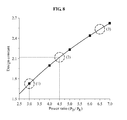
- FIGS. 7 and 8 are diagrams illustrating examples of a design constant of a target resonator and a power ratio.
- FIG. 9 is a diagram illustrating an example of a design of a target resonator.
- FIG. 10 is a diagram illustrating an example of a power division of target resonators.
- FIG. 11 is a flowchart illustrating an example of a method of designing a target resonator.
- FIG. 12 is a block diagram illustrating an example of an apparatus configured to determine a design parameter of a target resonator.
- FIGS. 13A through 14B are diagrams illustrating examples of applications in which a wireless power receiver and a wireless power transmitter may be mounted.
- FIG. 15 is a diagram illustrating an example of a wireless power transmitter and a wireless power receiver.
- FIG. 16 is a diagram illustrating an example of an electric vehicle charging system.
- FIG. 1 is a diagram illustrating an example of a wireless power transmission and charging system.
- the wireless power transmission and charging system includes a source device 110 and a target device 120 .
- the source device 110 is a device supplying wireless power, and may be any of various devices that supply power, such as pads, terminals, televisions (TVs), and any other device that supplies power.
- the target device 120 is a device receiving wireless power, and may be any of various devices that consume power, such as terminals, TVs, vehicles, washing machines, radios, lighting systems, and any other device that consumes power.
- the source device 110 includes an alternating current-to-direct current (AC/DC) converter 111 , a power detector 113 , a power converter 114 , a control and communication (control/communication) unit 115 , and a source resonator 116 .
- AC/DC alternating current-to-direct current
- the target device 120 includes a target resonator 121 , a rectification unit 122 , a DC-to-DC (DC/DC) converter 123 , a switch unit 124 , a device load 125 , and a control/communication unit 126 .
- the AC/DC converter 111 generates a DC voltage by rectifying an AC voltage having a frequency of tens of hertz (Hz) output from a power supply 112 .
- the AC/DC converter 111 may output a DC voltage having a predetermined level, or may output a DC voltage having an adjustable level by the control/communication unit 115 .
- the power detector 113 detects an output current and an output voltage of the AC/DC converter 111 , and provides, to the control/communication unit 115 , information on the detected current and the detected voltage. Additionally, the power detector 113 detects an input current and an input voltage of the power converter 114 .
- the power converter 114 generates a power by converting the DC voltage output from the AC/DC converter 111 to an AC voltage using a switching pulse signal having a frequency of a few kilohertz (kHz) to tens of megahertz (MHz).
- the power converter 114 converts a DC voltage supplied to a power amplifier to an AC voltage using a reference resonance frequency F Ref , and generates a wake-up power or a charging power to be used for charging that may be used in a plurality of target devices.
- the wake-up power may be, for example, a low power of 0.1 to 1 milliwatts (mW) that may be used by a target device to perform communication
- the charging power may be, for example, a high power of 1 mW to 200 Watts (W) that may be consumed by a device load of a target device.
- the term “charging” may refer to supplying power to an element or a unit that charges a battery or other rechargeable device with power.
- the term “charging” may refer supplying power to an element or a unit that consumes power.
- the term “charging power” may refer to power consumed by a target device while operating, or power used to charge a battery of the target device.
- the unit or the element may include, for example, a battery, a display device, a sound output circuit, a main processor, and various types of sensors.
- control/communication unit 115 may control a frequency of the switching pulse signal used by the power converter 114 .
- the control/communication unit 115 may perform out-of-band communication using a communication channel.
- the control/communication unit 115 may include a communication module, such as a ZigBee module, a Bluetooth module, or any other communication module, that the control/communication unit 115 may use to perform the out-of-band communication.
- the control/communication unit 115 may transmit or receive data to or from the target device 120 via the out-of-band communication.
- the source resonator 116 transfers electromagnetic energy, such as the wake-up power or the charging power, to the target resonator 121 via a magnetic coupling with the target resonator 121 .
- the target resonator 121 receives the electromagnetic energy, such as the wake-up power or the charging power, from the source resonator 116 via a magnetic coupling with the source resonator 116 . Additionally, the target resonator 121 receives various messages from the source device 110 via the in-band communication.
- a figure of merit (FOM) of the target resonator 121 satisfies a power dividing ratio of the source device 110 .
- the FOM of the target resonator 121 and the power dividing ratio will be further described with reference to FIGS. 2 through 10 .
- the rectification unit 122 generates a DC voltage by rectifying an AC voltage received by the target resonator 121 .
- the DC/DC converter 123 adjusts a level of the DC voltage output from the rectification unit 122 based on a voltage rating of the device load 125 .
- the DC/DC converter 123 may adjust the level of the DC voltage output from the rectification unit 122 to a level in a range from 3 volts (V) to 10 V.
- the switch unit 124 is turned on or off by the control/communication unit 126 .
- the control/communication unit 115 of the source device 110 may detect a reflected wave.
- the switch unit 124 is turned off, the magnetic coupling between the source resonator 116 and the target resonator 121 is interrupted.
- the device load 125 may include a battery.
- the device load 125 may charge the battery using the DC voltage output from the DC/DC converter 123 .
- the control/communication unit 126 is activated by the wake-up power.
- the control/communication unit 126 communicates with the source device 110 , and controls an operation of the target device 120 .
- the rectification unit 122 , the DC/DC converter 123 , and the switch unit 124 may be referred to as power supply units. Accordingly, the target device 120 includes the target resonator 121 and the power supply units 122 , 123 and 124 configured to supply the received power to the device load 125 .
- the device load 125 may be briefly expressed as a load.
- FIG. 2 illustrates an example of a multi-target environment.
- a source device 210 simultaneously, wirelessly transfers energy and data to target devices, for example, target devices 221 , 223 , and 225 . That is, based on a wireless power transmission employing a resonance scheme, the source device 210 simultaneously charges the target devices 221 , 223 , and 225 .
- the target devices 221 , 223 , and 225 may be of various types.
- the target device 221 may be a smartphone, a tablet personal computer (PC), and/or an MP3 (Moving Picture Experts Group Audio Layer III) player.
- the target devices 223 and 225 may be of the same type as, or a different type from, the target device 221 .
- the power may need to be divided based on an amount of power required by each of the target devices 221 , 223 , and 225 .
- each of the target devices 221 , 223 , and 225 may need to receive the required power.
- the power required by each of the target devices 221 , 223 , and 225 may refer to a power used to operate a device load, and/or a power required to completely charge a device load.
- the target device 221 When the target device 221 receives the power less than the amount of the power required by the target device 221 , the target device 221 may not operate, and/or a long period of time may be required to charge the target device 221 .
- the target device 221 receives the power greater than the amount of the required power, an error may occur in the target device 221 due to overvoltage or overcurrent. In other words, when the power is not correctly divided in the multi-target environment, a transmission efficiency may decrease, a device may malfunction, and/or the power may be wasted.
- a wireless power transmission system enabling an optimum power division, while maintaining a maximum power transmission efficiency of the wireless power transmission system.
- a method of designing a target resonator based on a power transmission efficiency and a power division is provided.
- FIG. 3 illustrates an example of a ratio of a dissipation power to a total required power in the multi-target environment of FIG. 2 .
- a horizontal axis represents an amount of normalized power
- a vertical axis represents a power dividing ratio.
- the amount of the normalized power is obtained by dividing an amount of power to be received by a target device (i.e., the dissipation power), by a total amount of power to be transmitted by a source device (i.e., the total required power).
- the source device 210 may transmit a total power of 10 W. Accordingly, when a power of 2 W is received by the target device 221 , a power of 3 W is received by the target device 223 , and a power of 4 W is received by the target device 225 , a normalized power of 0.2 W, a normalized power of 0.3 W, and a normalized power of 0.4 W may be obtained, respectively. Additionally, power dividing ratios for the target devices 221 , 223 , and 225 may be 20%, 30%, and 40%, respectively.
- the power dividing ratios of the source device 210 are obtained by dividing an amount of power to be received by each of the target devices 221 , 223 and 225 (i.e., the dissipation power), by a total amount of power to be transmitted by the source device 210 (i.e., the total required power).
- an optimum power division may be enabled.
- FIGS. 4 and 5 illustrate examples of problems occurring when power division is not considered.
- FIG. 4 illustrates an example in which a power is not divided correctly when a magnetic field of a source resonator is not uniform.
- a power division may be controlled using a matching network; however, an extremely large number of controls may be required. Additionally, when a large number of target devices exist, it may be difficult to divide a power using the matching network.
- Efficiency_T 1 indicates a power reception efficiency of a target device T 1
- Efficiency_T 2 indicates a power reception efficiency of a target device T 2
- Efficiency_Total indicates a total power reception efficiency of the target devices T 1 and T 2 .
- the Efficiency_T 1 may be 83%, but the Efficiency_T 2 may be 10%.
- the Efficiency_Total may be 93%.
- FIG. 5 illustrates an example in which a power dividing ratio is not satisfied due to a wrong design of a target resonator, despite a uniform magnetic field of a source resonator.
- an amount of power required by a target device T 1 may be 6.5 W and 3 W, respectively. Since an amount of power received by the target device T 1 may be almost identical to an amount of power received by the target device T 2 , a problem may occur in a power division.
- the target device T 1 when the target device T 1 receives a power less than the amount of the required power, it may be impossible to charge the target device T 1 , and/or a period of time longer than necessary may be required to charge the target device T 1 .
- the target device T 2 when the target device T 2 receives an extremely high power, the target device T 2 may be damaged due to overvoltage or overcurrent, and a total power transmission efficiency may be reduced.
- T 1 _Effi. indicates a power reception efficiency of a target device T 1
- T 2 _Effi. indicates a power reception efficiency of a target device T 2
- Total_Effi. indicates a total power reception efficiency of the target devices T 1 and T 2 .
- the T 1 _Effi. may be 40%
- the T 2 _Effi. may be 40%
- the Total_Effi. may be 80%.
- a condition required to satisfy the optimum power division in the multi-target environment is determined based on a FOM of a target resonator.
- a FOM of a target resonator there is a need to design the FOM of the target resonator to satisfy a power dividing ratio of a power transmitter.
- the optimum power division may be realized in the multi-target environment.
- a target device in the multi-target environment may be expressed as a target resonator, for convenience of description.
- the power dividing ratio may be determined based on the following example of Equation 1:
- Equation 1 ⁇ denotes a total power transmission efficiency in the multi-target environment.
- the total power transmission efficiency refers to a ratio of a power received by each of target resonators to a power output from a source device.
- the power dividing ratio refers to a ratio of a power amount of a load of a first target device to a power amount of a second target device, i.e., a reference device.
- the first target device and the second target device may receive power at the same time.
- the power amount of the load refers to an amount of power required by the load.
- N denotes a number of the target resonators.
- U 0n denotes a FOM of an n-th target resonator with respect to the source device.
- Equation 1 In the multi-target environment, in a condition in which impedance matching is completed, Equation 1 may be expressed as shown in the following example of Equation 2:
- the power dividing ratio ⁇ n of the power transmitter may be expressed as shown in the example of Equation 3 below.
- the power dividing ratio of the power transmitter may be expressed as a power dividing ratio.
- Total Efficiency refers to the total power transmission efficiency of the wireless power transmission system. Additionally, “Efficiency of n-th target” refers to a power reception efficiency of an n-th target resonator.
- the power dividing ratio may be expressed in terms of the FOM of the n-the target resonator.
- the FOM of the n-th target resonator may be expressed in terms of the quality factor of the n-th target resonator and the coupling coefficient of the source resonator and the n-th target resonator.
- an FOM of a target resonator may be determined.
- the FOM U D of the target resonator determined based on the power dividing ratio may be expressed as shown in the following example of Equation 4:
- Equation 4 X denotes a normalized power dividing ratio, P R denotes a reference power amount, P D denotes a power amount of a load, namely, a device load, and DC denotes a design constant of the target resonator.
- the reference power amount may refer to a maximum amount of power required by a reference device, for example, 1 W.
- the reference device may be a virtual device configured to determine a reference FOM U ref of the source device or the source resonator. Additionally, the reference device may be a predetermined device configured to determine the reference FOM U ref .
- the FOM of the target resonator may be determined based on the reference FOM U ref of the source resonator, and a design constant DC set in advance. Additionally, the FOM of the target resonator may be determined based on a ratio P D /P R of the power amount of the load connected to the target resonator to the reference power amount, namely, the amount of the power required by the reference device. For example, when a dissipation power of a load, or a maximum amount of power that may be received by the load, is 100 W, the ratio P D /P R may be determined to be in a range of 85 W to 115 W. That is, the power amount of the load to determine the FOM of the target resonator may be in the range of 85% to 115% of the dissipation power of the load.
- Equation 5 k ref denotes a coupling coefficient of the reference device, Q 0 denotes the quality factor of the source resonator, and Q ref denotes a quality factor of the reference device.
- a value of the FOM U D satisfying Equation 4 may be determined by adjusting a coupling coefficient k D of the target resonator, and a quality factor Q D of the target resonator.
- Equation 6 The coupling coefficient k D and the quality factor Q D in Equation 6 may be expressed as shown in the following examples of Equations 7 and 8, respectively:
- Equation 7 M denotes a mutual inductance between the source resonator and the target resonator, L 0 denotes an inductance value of the source resonator, and L D denotes an inductance value of the target resonator.
- ⁇ denotes a value determined by representing a resonance frequency as an angular speed
- R D _ rad denotes a conductor resistance value of the target resonator
- R D _ loss denotes a conductor loss value of the target resonator.
- FIG. 6 illustrates an example of a design constant of a target resonator and an amount of normalized power dividing ratio.
- a horizontal axis represents a normalized power dividing ratio X in Equation 4
- a vertical axis represents a design constant of a target resonator.
- a power amount P D of the target resonator to be designed may include an infinite value.
- a design constant may be 1.
- the target resonator to be designed may receive a power lower than a power received by a reference device.
- the target resonator may be designed based on information regarding the reference device.
- a FOM of the target resonator satisfies Equation 4
- an optimum power division may be enabled in a multi-target environment.
- the FOM of the target resonator may be designed or determined to satisfy Equation 4.
- FIGS. 7 and 8 illustrate examples of a design constant of a target resonator and a power ratio.
- a horizontal axis represents a power ratio P D /P R of a target device to a source device
- a vertical axis represents a design constant of a target resonator.
- Graphs of FIGS. 7 and 8 may be acquired from Equations 4 through 7. For example, data shown in FIGS. 7 and 8 may be stored in a lookup table. When a value of the power ratio P D /P R is input, a computer system may output information on a design constant matched to the value of the power ratio P D /P R .
- a power dividing ratio may be normally maintained.
- the design range is determined based on a reference FOM of a source resonator, and a design constant set in advance.
- a power division may not be maintained normally.
- the design constant of the target resonator may include a determined value of
- the error margin R design of the design constant may need to satisfy the following example of Condition 1: 0.95 ⁇ DC ⁇ R design ⁇ 1.05 ⁇ DC [Condition 1]
- the design constant when the power ratio is 6.5, the design constant may be 2.55, as indicated by a point 701 .
- the design constant includes an extremely small value, compared to the power ratio, and accordingly, when the design constant is beyond the error margin, the power dividing ratio may be difficult to maintain.
- Table 1 illustrates an example of a lookup table in which the data of FIGS. 7 and 8 is stored.
- a reference device Ref requires a power of 1 W
- a normalized power dividing ratio X includes a value of 0.5
- a design constant DC is 1.
- the design constant DC is 1.73.
- the design constant DC is 2.12.
- the design constant DC is 2.55.
- the reference device Ref may require a power of 1 W, a power greater than or less than 1 W, and/or both.
- a normal power division may be enabled in a multi-target environment.
- the normal power division may include an error margin within 15% of a power amount of each of the target devices.
- a power of 2.8 W is required to smoothly charge a first target device
- the first target device may be determined to receive the power that is normally divided.
- power of 6 W is required to smoothly charge a second target device
- the second target device may be determined to receive the power that is normally divided.
- a value of an FOM of a target resonator may be determined by multiplication of a quality factor Q and a coupling coefficient k of the target resonator.
- the quality factor Q and the coupling coefficient k may be used as design parameters of the target resonator.
- the quality factor Q may be adjusted based on a conductor loss of the target resonator, a conductor resistance of the target resonator, and/or an inductance of the target resonator. A value of a resonance frequency may remain unchanged.
- the coupling coefficient k may be adjusted based on a size of the target resonator, a thickness of a conductor included in the target resonator, and/or a width of the conductor.
- the design parameters of the target resonator may be determined based on the FOM of the target resonator. Values of the design parameters may be combined in countless combinations, and may be determined based on Equations 5 through 8.
- FIG. 9 illustrates an example of a design of a target resonator.
- the target resonator includes a shape of a rectangular loop.
- a FOM of the target resonator may be determined based on Equations 7 and 8.
- a value of an inductance of the target resonator used to obtain the FOM may be expressed as shown in the following example of Equation 9:
- the value of the inductance of the target resonator to be designed may be adjusted based on numerical values a, b, c, d, and g associated with the shape of the target resonator.
- a denotes a horizontal distance of the target resonator
- b denotes a vertical distance of the target resonator
- c denotes a horizontal thickness of the target resonator
- d denotes a thickness between opposite faces of the target resonator
- g denotes a diagonal distance between the thicknesses c and d.
- the expression described in Equation 9 may be used to determine the value of the inductance of the rectangular loop-shaped resonator.
- an equation, such as Equation 9 may be induced using a simulation result of the target resonator.
- FIG. 10 illustrates an example of a power division of target resonators.
- T 1 indicates a target device requiring a power of 3 W
- T 2 indicates a target device requiring a power of 4.5 W
- T 3 indicates a target device requiring a power of 6.5 W.
- a total amount of power transmitted by a source device is 14 W.
- a target resonator of the target device T 1 may include a design constant of 1, and a target resonator of the target device T 2 may include a design constant of 1.73. Additionally, a target resonator of the target device T 3 may include a design constant of 2.55. Due to the power division and the design constants of the target resonators, each of the target devices T 1 , T 2 , and T 3 receives a power based on the respective amounts of the required power, and at optimum respective power reception efficiencies. For example, at a resonance frequency of 13.56 MHz, the target device T 1 receives a power of 3 W, which corresponds to the amount of the required power, and at an optimal power reception efficiency of about 20%.
- FIG. 11 illustrates an example of a method of designing a target resonator.
- the method of FIG. 11 may be performed by a computer system.
- the computer system may be operated as a design parameter determining apparatus configured to determine design parameters of the target resonator to be designed.
- the method of FIG. 11 is assumed to be performed by a processor.
- the processor receives information on a power amount of a load connected to the target resonator.
- the information on the power amount of the load may be automatically-selected based on an input of a model name of a corresponding target device, a type of the target device, a model number of the target device, and/or other information known to one of ordinary skill in the art. For example, when a smartphone is used as the target device and includes a model number of PHY-3, a power amount of a load connected to the smartphone may be determined to be 3 W based on the mode number of PHY-3.
- the processor determines a FOM of the target resonator based on the received information.
- the FOM satisfies a power dividing ratio of a power transmitter.
- the FOM satisfying the power dividing ratio may be determined based on the data of FIGS. 7 and 8 and/or the data of Table 1.
- the FOM may be determined based on the power amount the load, a reference FOM of a source resonator of the power transmitter, and a design constant of the target resonator.
- the FOM satisfying the power dividing ratio may be determined based on a type of the target resonator.
- the processor determines a design parameter of the target resonator based on the FOM. For example, the processor may determine and output or display a value of a quality factor Q and a value of a coupling coefficient k, of the target resonator, that are suitable for the FOM, and/or may store the values in a memory. Additionally, the processor may determine the design parameter based on the design constant.
- the design parameter may include, for example, a size of the target resonator, a thickness of a conductor included in the target resonator, a width of the conductor, a loss of the conductor, a resistance of the conductor, and/or an inductance value of the target resonator.
- FIG. 12 illustrates an example of an apparatus 1200 configured to determine a design parameter of a target resonator.
- the apparatus 1200 may perform the method of FIG. 11 .
- the apparatus 1200 includes an input unit 1210 , a FOM determining unit 1220 , and a design parameter determining unit 1230 .
- the input unit 1210 receives information on a power amount of a load connected to the target resonator.
- the input unit 1210 may include, for example, a user interface enabling a user to enter the information on the power amount of the load.
- the FOM determining unit 1220 determines a FOM of the target resonator based on a lookup table and the received information on the power amount of the load.
- the FOM satisfies a power dividing ratio of a power transmitter.
- the lookup table may include the data of FIGS. 7 and 8 and/or the data of Table 1.
- the FOM determining unit 1220 may include a memory configured to store all information required to determine the FOM, such as a reference FOM of a source resonator of the power transmitter.
- the design parameter determining unit 1230 determines a design parameter of the target resonator based on the FOM.
- the processor may determine and output or display a value of a quality factor Q and a value of a coupling coefficient k, of the target resonator, that are suitable for the FOM, and/or may store the values in a memory.
- FIGS. 13A through 14B illustrate examples of applications in which a wireless power receiver and a wireless power transmitter may be mounted.
- FIG. 13A illustrates an example of wireless power charging between a pad 1310 and a mobile terminal 1320
- FIG. 13B illustrates an example of wireless power charging between pads 1330 and 1340 and hearing aids 1350 and 1360 , respectively.
- a wireless power transmitter is mounted in the pad 1310
- a wireless power receiver is mounted in the mobile terminal 1320 .
- the pad 1310 charges a single mobile terminal, namely, the mobile terminal 1320 .
- two wireless power transmitters are respectively mounted in the pads 1330 and 1340 .
- the hearing aids 1350 and 1360 are used for a left ear and a right ear, respectively.
- Two wireless power receivers are respectively mounted in the hearing aids 1350 and 1360 .
- the pads 1330 and 1340 charge two hearing aids, respectively, namely, the hearing aids 1350 and 1360 .
- FIG. 14A illustrates an example of wireless power charging between an electronic device 1410 inserted into a human body, and a mobile terminal 1420 .
- FIG. 14B illustrates an example of wireless power charging between a hearing aid 1430 and a mobile terminal 1440 .
- a wireless power transmitter and a wireless power receiver are mounted in the mobile terminal 1420 .
- Another wireless power receiver is mounted in the electronic device 1410 .
- the electronic device 1410 is charged by receiving a power from the mobile terminal 1420 .
- a wireless power transmitter and a wireless power receiver are mounted in the mobile terminal 1440 .
- Another wireless power receiver is mounted in the hearing aid 1430 .
- the hearing aid 1430 is charged by receiving a power from the mobile terminal 1440 .
- Low-power electronic devices for example, Bluetooth earphones, may also be charged by receiving a power from the mobile terminal 1440 .
- FIG. 15 illustrates an example of a wireless power transmitter 1510 and a wireless power receiver 1520 .
- the wireless power transmitter 1510 may be mounted in each of the pad 1310 of FIG. 13A and pads 1330 and 1340 of FIG. 13B . Additionally, the wireless power transmitter 1510 may be mounted in each of the mobile terminal 1420 of FIG. 14A and the mobile terminal 1440 of FIG. 14B .
- the wireless power receiver 1520 may be mounted in each of the mobile terminal 1320 of FIG. 13A and the hearing aids 1350 and 1360 of FIG. 13B . Further, the wireless power receiver 1520 may be mounted in each of the electronic device 1410 of FIG. 14A and the hearing aid 1430 of FIG. 14B .
- the wireless power transmitter 1510 may include a similar configuration to the source device 110 of FIG. 1 .
- the wireless power transmitter 1510 may include a unit configured to transmit a power using magnetic coupling.
- the wireless power transmitter 1510 includes a signal generator, a power amplifier, a microcontroller unit (MCU), a source resonator, and a communication/tracking unit 1511 .
- the communication/tracking unit 1511 communicates with the wireless power receiver 1520 , and controls an impedance and a resonance frequency to maintain a wireless power transmission efficiency. Additionally, the communication/tracking unit 1511 may perform similar functions to the power converter 114 and the control/communication unit 115 of FIG. 1 .
- the wireless power receiver 1520 may include a similar configuration to the target device 120 of FIG. 1 .
- the wireless power receiver 1520 may include a unit configured to wirelessly receive a power and to charge a battery.
- the wireless power receiver 1520 includes a target resonator, a rectifier, a DC/DC converter, and a charging circuit. Additionally, the wireless power receiver 1520 includes a communication/control unit 1523 . The communication/control unit 1523 communicates with the wireless power transmitter 1510 , and performs an operation to protect overvoltage and overcurrent.
- the wireless power receiver 1520 may include a hearing device circuit 1521 .
- the hearing device circuit 1521 may be charged by a battery.
- the hearing device circuit 1521 may include a microphone, an analog-to-digital converter (ADC), a processor, a digital-to-analog converter (DAC), and a receiver.
- ADC analog-to-digital converter
- DAC digital-to-analog converter
- the hearing device circuit 1521 may include the same configuration as a hearing aid.
- FIG. 16 illustrates an example of an electric vehicle charging system.
- an electric vehicle charging system 1600 includes a source system 1610 , a source resonator 1620 , a target resonator 1630 , a target system 1640 , and an electric vehicle battery 1650 .
- the electric vehicle charging system 1600 has a structure similar to the structure of the wireless power transmission system of FIG. 1 .
- the source system 1610 and the source resonator 1620 in the electric vehicle charging system 1600 operate as a source.
- the target resonator 1630 and the target system 1640 in the electric vehicle charging system 1600 operate as a target.
- the source system 1610 includes an alternating current-to-direct current (AC/DC) converter, a power detector, a power converter, a control and communication (control/communication) unit similar to those of the source device 110 of FIG. 1 .
- the target system 1640 includes a rectification unit, a DC-to-DC (DC/DC) converter, a switch unit, a charging unit, and a control/communication unit similar to those of the target device 120 of FIG. 1 .
- the electric vehicle battery 1650 is charged by the target system 1640 .
- the electric vehicle charging system 1600 may use a resonant frequency in a band of a few kHz to tens of MHz.
- the source system 1610 generates power based on a type of the vehicle being charged, a capacity of the electric vehicle battery 1650 , and a charging state of the electric vehicle battery 1650 , and wirelessly transmits the generated power to the target system 1640 via a magnetic coupling between the source resonator 1620 and the target resonator 1630 .
- the source system 1610 may control an alignment of the source resonator 1620 and the target resonator 1630 .
- the controller of the source system 1610 may transmit a message to the target system 1640 to control the alignment of the source resonator 1620 and the target resonator 1630 .
- the source system 1610 may instruct a position of the vehicle to be adjusted to control the source resonator 1620 and the target resonator 1630 to be aligned.
- this is just an example, and other methods of aligning the source resonator 1620 and the target resonator 1630 may be used.
- the source system 1610 and the target system 1640 may transmit or receive an ID of a vehicle and exchange various messages by performing communication with each other.
- the electric vehicle charging system 1600 may use a resonant frequency in a band of a few kHz to tens of MHz, and may wirelessly transmit power that is equal to or higher than tens of watts to charge the electric vehicle battery 1650 .
- a resonator enabling optimum power division, and a method of designing the resonator, in a wireless power transmission environment in which various target devices exist.
- the units described herein may be implemented using hardware components and software components.
- the hardware components may include microphones, amplifiers, band-pass filters, audio to digital convertors, and processing devices.
- a processing device may be implemented using one or more general-purpose or special purpose computers, such as, for example, a processor, a controller and an arithmetic logic unit, a digital signal processor, a microcomputer, a field programmable array, a programmable logic unit, a microprocessor or any other device capable of responding to and executing instructions in a defined manner.
- the processing device may run an operating system (OS) and one or more software applications that run on the OS.
- the processing device also may access, store, manipulate, process, and create data in response to execution of the software.
- OS operating system
- a processing device may include multiple processing elements and multiple types of processing elements.
- a processing device may include multiple processors or a processor and a controller.
- different processing configurations are possible, such a parallel processors.
- the software may include a computer program, a piece of code, an instruction, or some combination thereof, to independently or collectively instruct or configure the processing device to operate as desired.
- Software and data may be embodied permanently or temporarily in any type of machine, component, physical or virtual equipment, computer storage medium or device, or in a propagated signal wave capable of providing instructions or data to or being interpreted by the processing device.
- the software also may be distributed over network coupled computer systems so that the software is stored and executed in a distributed fashion.
- the software and data may be stored by one or more computer readable recording mediums.
- the computer readable recording medium may include any data storage device that can store data which can be thereafter read by a computer system or processing device.
- non-transitory computer readable recording medium examples include read-only memory (ROM), random-access memory (RAM), CD-ROMs, magnetic tapes, floppy disks, optical data storage devices.
- ROM read-only memory
- RAM random-access memory
- CD-ROMs compact disc-read only memory
- magnetic tapes magnetic tapes
- floppy disks optical data storage devices.
- functional programs, codes, and code segments accomplishing the examples disclosed herein can be easily construed by programmers skilled in the art to which the examples pertain based on and using the flow diagrams and block diagrams of the figures and their corresponding descriptions as provided herein.
- Program instructions to perform a method described herein, or one or more operations thereof, may be recorded, stored, or fixed in one or more computer-readable storage media.
- the program instructions may be implemented by a computer.
- the computer may cause a processor to execute the program instructions.
- the media may include, alone or in combination with the program instructions, data files, data structures, and the like.
- Examples of non-transitory computer-readable storage media include magnetic media, such as hard disks, floppy disks, and magnetic tape; optical media such as CD ROM disks and DVDs; magneto-optical media, such as optical disks; and hardware devices that are configured to store and perform program instructions, such as read-only memory (ROM), random access memory (RAM), flash memory, and the like.
- Examples of program instructions include machine code, such as produced by a compiler, and files including higher level code that may be executed by the computer using an interpreter.
- the program instructions that is, software, may be distributed over network coupled computer systems so that the software is stored and executed in a distributed fashion.
- the software and data may be stored by one or more computer readable storage mediums.
- functional programs, codes, and code segments accomplishing the example examples disclosed herein can be easily construed by programmers skilled in the art to which the examples pertain based on and using the flow diagrams and block diagrams of the figures and their corresponding descriptions as provided herein.
- a terminal and a device described herein may refer to mobile devices such as a cellular phone, a personal digital assistant (PDA), a digital camera, a portable game console, and an MP3 player, a portable/personal multimedia player (PMP), a handheld e-book, a portable laptop PC, a global positioning system (GPS) navigation, a tablet, a sensor, and devices such as a desktop PC, a high definition television (HDTV), an optical disc player, a setup box, a home appliance, and the like that are capable of wireless communication or network communication consistent with that which is disclosed herein.
- mobile devices such as a cellular phone, a personal digital assistant (PDA), a digital camera, a portable game console, and an MP3 player, a portable/personal multimedia player (PMP), a handheld e-book, a portable laptop PC, a global positioning system (GPS) navigation, a tablet, a sensor, and devices such as a desktop PC, a high definition television (HDTV), an optical disc player, a
Landscapes
- Engineering & Computer Science (AREA)
- Power Engineering (AREA)
- Computer Networks & Wireless Communication (AREA)
- Transportation (AREA)
- Mechanical Engineering (AREA)
- Computer Hardware Design (AREA)
- Physics & Mathematics (AREA)
- Theoretical Computer Science (AREA)
- Evolutionary Computation (AREA)
- Geometry (AREA)
- General Engineering & Computer Science (AREA)
- General Physics & Mathematics (AREA)
- Charge And Discharge Circuits For Batteries Or The Like (AREA)
Abstract
Description
and
U ref =k ref√{square root over (Q 0 Q ref)},
0.95×DC≦R design≦1.05×DC
and
U ref =k ref√{square root over (Q 0 Q ref)},
U ref =k ref√{square root over (Q 0 Q ref)} [Equation 5]
U D =k D√{square root over (Q 0 Q D)} [Equation 6]
and include an error margin within 5%. In other words, the error margin Rdesign of the design constant may need to satisfy the following example of Condition 1:
0.95×DC≦R design≦1.05×DC [Condition 1]
of the target resonator.
| TABLE 1 | ||||
| PD | X = PD/(PD + PR) | DC = {square root over (X/(1 − X))} | ||
| Ref. | 1 | 0.5 | 1 | ||
| |
3 | 0.75 | 1.73 | ||
| T2 | 4.5 | 0.82 | 2.12 | ||
| T3 | 6.5 | 0.87 | 2.55 | ||
Claims (19)
U ref =k ref√{square root over (Q 0 Q ref)},
0.95×DC≦R design≦1.05×DC,
U ref =k ref√{square root over (Q 0 Q ref)},
U ref =k ref√{square root over (Q 0 Q ref)},
0.95×DC≦R design≦1.05×DC,
Applications Claiming Priority (2)
| Application Number | Priority Date | Filing Date | Title |
|---|---|---|---|
| KR1020110116025A KR101321436B1 (en) | 2011-11-08 | 2011-11-08 | Wireless power transmission system, resonator design method for optimal power distribution and resonator in wireless power transmission system |
| KR10-2011-0116025 | 2011-11-08 |
Publications (2)
| Publication Number | Publication Date |
|---|---|
| US20130113296A1 US20130113296A1 (en) | 2013-05-09 |
| US9643504B2 true US9643504B2 (en) | 2017-05-09 |
Family
ID=48223217
Family Applications (1)
| Application Number | Title | Priority Date | Filing Date |
|---|---|---|---|
| US13/614,098 Active 2035-06-30 US9643504B2 (en) | 2011-11-08 | 2012-09-13 | Wireless power transmission system, resonator in wireless power transmission system, and resonator design method for optimum power division |
Country Status (2)
| Country | Link |
|---|---|
| US (1) | US9643504B2 (en) |
| KR (1) | KR101321436B1 (en) |
Cited By (1)
| Publication number | Priority date | Publication date | Assignee | Title |
|---|---|---|---|---|
| US20150239354A1 (en) * | 2012-09-13 | 2015-08-27 | Toyota Jidosha Kabushiki Kaisha | Non-contact power supply system, and power transmission device and vehicle used therein |
Families Citing this family (20)
| Publication number | Priority date | Publication date | Assignee | Title |
|---|---|---|---|---|
| JP5071574B1 (en) * | 2011-07-05 | 2012-11-14 | ソニー株式会社 | Sensing device, power receiving device, non-contact power transmission system, and sensing method |
| CN103295079A (en) * | 2013-06-09 | 2013-09-11 | 国家电网公司 | Electric power multi-objective decision support method based on intelligent data mining model |
| CN103413254A (en) * | 2013-09-04 | 2013-11-27 | 国家电网公司 | Medium-and-long-term load prediction research and management integration application system |
| DE102013217816A1 (en) | 2013-09-06 | 2015-03-12 | Robert Bosch Gmbh | Device for inductive energy transmission and method for operating a device for inductive energy transmission |
| KR101579675B1 (en) * | 2014-03-14 | 2015-12-23 | 한국과학기술원 | System and method for detecting resonance frequency |
| WO2016022499A1 (en) | 2014-08-03 | 2016-02-11 | PogoTec, Inc. | Wearable camera systems and apparatus and method for attaching camera systems or other electronic devices to wearable articles |
| US9635222B2 (en) | 2014-08-03 | 2017-04-25 | PogoTec, Inc. | Wearable camera systems and apparatus for aligning an eyewear camera |
| KR101994737B1 (en) * | 2014-08-19 | 2019-07-01 | 삼성전기주식회사 | Wireless charging apparatus and method for the same |
| KR102231851B1 (en) | 2014-09-25 | 2021-03-26 | 삼성전자주식회사 | A method for recharging one or more eelectronic devices and a recharging apparatus therefor |
| CN107251364A (en) | 2014-12-23 | 2017-10-13 | 波戈技术有限公司 | wireless camera system and method |
| CN104574210A (en) * | 2015-01-08 | 2015-04-29 | 国家电网公司 | Full-dimension electricity market analyzing and researching method |
| EP3872559A1 (en) | 2015-06-10 | 2021-09-01 | Pogotec, Inc. | Electronic wearable device for an eyewear with magnetic track |
| US10481417B2 (en) | 2015-06-10 | 2019-11-19 | PogoTec, Inc. | Magnetic attachment mechanism for electronic wearable device |
| US10224752B2 (en) * | 2015-08-28 | 2019-03-05 | Qualcomm Incorporated | Method and apparatus for computer aided designing, tuning and matching of wireless power transfer systems |
| US10341787B2 (en) | 2015-10-29 | 2019-07-02 | PogoTec, Inc. | Hearing aid adapted for wireless power reception |
| US11558538B2 (en) | 2016-03-18 | 2023-01-17 | Opkix, Inc. | Portable camera system |
| US10863060B2 (en) | 2016-11-08 | 2020-12-08 | PogoTec, Inc. | Smart case for electronic wearable device |
| WO2020015746A1 (en) * | 2018-07-19 | 2020-01-23 | Mediatek Singapore Pte. Ltd. | Detecting foreign objects in wireless power transfer systems |
| US11300857B2 (en) | 2018-11-13 | 2022-04-12 | Opkix, Inc. | Wearable mounts for portable camera |
| KR20250098606A (en) | 2023-12-22 | 2025-07-01 | 주식회사 엘지에너지솔루션 | Data processing apparatus and method for analyzing battery manufacturing process |
Citations (8)
| Publication number | Priority date | Publication date | Assignee | Title |
|---|---|---|---|---|
| JP2010063245A (en) | 2008-09-02 | 2010-03-18 | Sony Corp | Non-contact feeder system |
| JP2010104203A (en) | 2008-10-27 | 2010-05-06 | Seiko Epson Corp | Power feed control apparatus, power feed apparatus, electric power-receiving control apparatus, electric power-receiving apparatus, electronic equipment, and contactless power transmission system |
| JP2010141977A (en) | 2008-12-09 | 2010-06-24 | Toyota Industries Corp | Power transmission method in non-contact power transmission apparatus, and the non-contact power transmission apparatus |
| WO2010116441A1 (en) | 2009-03-30 | 2010-10-14 | 富士通株式会社 | Wireless power supply system, wireless power transmission device, and wireless power receiving device |
| US20100276995A1 (en) | 2009-04-29 | 2010-11-04 | Thomas Louis Marzetta | Security for wireless transfer of electrical power |
| WO2011061821A1 (en) * | 2009-11-18 | 2011-05-26 | 株式会社 東芝 | Wireless power transmission device |
| KR20110094382A (en) | 2010-02-16 | 2011-08-24 | 서울대학교산학협력단 | Multiple Wireless Power Transmission Method and System Using Time Division Method |
| KR20110099485A (en) | 2010-03-02 | 2011-09-08 | 전자부품연구원 | Multi-node wireless energy transmission system using resonant magnetic induction |
Family Cites Families (1)
| Publication number | Priority date | Publication date | Assignee | Title |
|---|---|---|---|---|
| KR101136532B1 (en) * | 2009-09-15 | 2012-04-17 | 주식회사 삼보컴퓨터 | Contactless charging device, contactless charging battery device and contactless charging system comprising the same |
-
2011
- 2011-11-08 KR KR1020110116025A patent/KR101321436B1/en not_active Expired - Fee Related
-
2012
- 2012-09-13 US US13/614,098 patent/US9643504B2/en active Active
Patent Citations (10)
| Publication number | Priority date | Publication date | Assignee | Title |
|---|---|---|---|---|
| JP2010063245A (en) | 2008-09-02 | 2010-03-18 | Sony Corp | Non-contact feeder system |
| JP2010104203A (en) | 2008-10-27 | 2010-05-06 | Seiko Epson Corp | Power feed control apparatus, power feed apparatus, electric power-receiving control apparatus, electric power-receiving apparatus, electronic equipment, and contactless power transmission system |
| JP2010141977A (en) | 2008-12-09 | 2010-06-24 | Toyota Industries Corp | Power transmission method in non-contact power transmission apparatus, and the non-contact power transmission apparatus |
| WO2010116441A1 (en) | 2009-03-30 | 2010-10-14 | 富士通株式会社 | Wireless power supply system, wireless power transmission device, and wireless power receiving device |
| US20100276995A1 (en) | 2009-04-29 | 2010-11-04 | Thomas Louis Marzetta | Security for wireless transfer of electrical power |
| WO2011061821A1 (en) * | 2009-11-18 | 2011-05-26 | 株式会社 東芝 | Wireless power transmission device |
| US20120235509A1 (en) * | 2009-11-18 | 2012-09-20 | Kabushiki Kaisha Toshiba | Wireless power transmission device |
| JPWO2011061821A1 (en) * | 2009-11-18 | 2013-04-04 | 株式会社東芝 | Wireless power transmission device |
| KR20110094382A (en) | 2010-02-16 | 2011-08-24 | 서울대학교산학협력단 | Multiple Wireless Power Transmission Method and System Using Time Division Method |
| KR20110099485A (en) | 2010-03-02 | 2011-09-08 | 전자부품연구원 | Multi-node wireless energy transmission system using resonant magnetic induction |
Cited By (2)
| Publication number | Priority date | Publication date | Assignee | Title |
|---|---|---|---|---|
| US20150239354A1 (en) * | 2012-09-13 | 2015-08-27 | Toyota Jidosha Kabushiki Kaisha | Non-contact power supply system, and power transmission device and vehicle used therein |
| US9963040B2 (en) * | 2012-09-13 | 2018-05-08 | Toyota Jidosha Kabushiki Kaisha | Non-contact power supply system, and power transmission device and vehicle used therein |
Also Published As
| Publication number | Publication date |
|---|---|
| KR101321436B1 (en) | 2013-11-04 |
| US20130113296A1 (en) | 2013-05-09 |
| KR20130050782A (en) | 2013-05-16 |
Similar Documents
| Publication | Publication Date | Title |
|---|---|---|
| US9643504B2 (en) | Wireless power transmission system, resonator in wireless power transmission system, and resonator design method for optimum power division | |
| US9997959B2 (en) | Wireless power transmission system and method for increasing coupling efficiency by adjusting resonant frequency | |
| US10315525B2 (en) | Source device and method for controlling magnetic field using two source resonators in wireless power transmission system | |
| US9706307B2 (en) | Sound system using wireless power transmission | |
| US9112367B2 (en) | Wireless power transmission system, method and apparatus for tracking resonance frequency in wireless power transmission system | |
| US9748800B2 (en) | Wireless power transmission system, and method of controlling power in wireless power transmission system based on detection parameter | |
| US9350193B2 (en) | Method and apparatus for detecting load fluctuation of wireless power transmission | |
| US9543074B2 (en) | Apparatus and method for wireless power reception, apparatus and method for wireless power transmission, and wireless power transmission system | |
| US9608452B2 (en) | Wireless power transmission system, and method and apparatus for controlling power in wireless power transmission system | |
| US10205353B2 (en) | Apparatus and method for charging control in wireless charging system | |
| US9178568B2 (en) | Apparatus and method for communication using wireless power | |
| US9425863B2 (en) | Apparatus and method for wirelessly receiving power, and apparatus and method for wirelessly transmitting power | |
| CN106133857B (en) | System, apparatus and method for wireless power receiver coil configuration | |
| US9882426B2 (en) | Method and apparatus for detecting efficiency of wireless power transmission | |
| US9287735B2 (en) | Wireless power transmission system and multi-mode resonator in wireless power transmission system | |
| US20130113298A1 (en) | Wireless power transmission system and method based on impedance matching condition | |
| US9437362B2 (en) | Apparatus and method for wireless power reception | |
| US9502174B2 (en) | Wireless power transmission apparatus and wireless power reception apparatus | |
| US20140375256A1 (en) | Wireless power transmission system with ability to determine charging circumstances | |
| US20140080409A1 (en) | Static tuning of wireless transmitters | |
| US9673872B2 (en) | Multi-band transmit antenna | |
| US10199871B2 (en) | Apparatus and method for wireless power charging of subsequent receiver | |
| KR20160087870A (en) | Method and apparatus for wireless energy transmission and reception | |
| US20170133860A1 (en) | System And Method Of Wireless Power Transfer Without Data Communication Channel |
Legal Events
| Date | Code | Title | Description |
|---|---|---|---|
| AS | Assignment |
Owner name: SAMSUNG ELECTRONICS CO., LTD., KOREA, REPUBLIC OF Free format text: ASSIGNMENT OF ASSIGNORS INTEREST;ASSIGNORS:RYU, YOUNG HO;PARK, EUN SEOK;KWON, SANG WOOK;AND OTHERS;REEL/FRAME:028956/0059 Effective date: 20120824 |
|
| STCF | Information on status: patent grant |
Free format text: PATENTED CASE |
|
| FEPP | Fee payment procedure |
Free format text: PAYOR NUMBER ASSIGNED (ORIGINAL EVENT CODE: ASPN) |
|
| MAFP | Maintenance fee payment |
Free format text: PAYMENT OF MAINTENANCE FEE, 4TH YEAR, LARGE ENTITY (ORIGINAL EVENT CODE: M1551); ENTITY STATUS OF PATENT OWNER: LARGE ENTITY Year of fee payment: 4 |
|
| MAFP | Maintenance fee payment |
Free format text: PAYMENT OF MAINTENANCE FEE, 8TH YEAR, LARGE ENTITY (ORIGINAL EVENT CODE: M1552); ENTITY STATUS OF PATENT OWNER: LARGE ENTITY Year of fee payment: 8 |