US9614192B2 - Method for forming thin film and method for fabricating organic light-emitting diode (OLED) display using the same - Google Patents
Method for forming thin film and method for fabricating organic light-emitting diode (OLED) display using the same Download PDFInfo
- Publication number
- US9614192B2 US9614192B2 US14/487,946 US201414487946A US9614192B2 US 9614192 B2 US9614192 B2 US 9614192B2 US 201414487946 A US201414487946 A US 201414487946A US 9614192 B2 US9614192 B2 US 9614192B2
- Authority
- US
- United States
- Prior art keywords
- substrate
- thin film
- forming
- deposition source
- shadow masks
- Prior art date
- Legal status (The legal status is an assumption and is not a legal conclusion. Google has not performed a legal analysis and makes no representation as to the accuracy of the status listed.)
- Expired - Fee Related, expires
Links
Images


Classifications
-
- H—ELECTRICITY
- H05—ELECTRIC TECHNIQUES NOT OTHERWISE PROVIDED FOR
- H05B—ELECTRIC HEATING; ELECTRIC LIGHT SOURCES NOT OTHERWISE PROVIDED FOR; CIRCUIT ARRANGEMENTS FOR ELECTRIC LIGHT SOURCES, IN GENERAL
- H05B33/00—Electroluminescent light sources
- H05B33/10—Apparatus or processes specially adapted to the manufacture of electroluminescent light sources
-
- H—ELECTRICITY
- H10—SEMICONDUCTOR DEVICES; ELECTRIC SOLID-STATE DEVICES NOT OTHERWISE PROVIDED FOR
- H10K—ORGANIC ELECTRIC SOLID-STATE DEVICES
- H10K71/00—Manufacture or treatment specially adapted for the organic devices covered by this subclass
- H10K71/10—Deposition of organic active material
- H10K71/12—Deposition of organic active material using liquid deposition, e.g. spin coating
- H10K71/13—Deposition of organic active material using liquid deposition, e.g. spin coating using printing techniques, e.g. ink-jet printing or screen printing
-
- H01L51/56—
-
- C—CHEMISTRY; METALLURGY
- C23—COATING METALLIC MATERIAL; COATING MATERIAL WITH METALLIC MATERIAL; CHEMICAL SURFACE TREATMENT; DIFFUSION TREATMENT OF METALLIC MATERIAL; COATING BY VACUUM EVAPORATION, BY SPUTTERING, BY ION IMPLANTATION OR BY CHEMICAL VAPOUR DEPOSITION, IN GENERAL; INHIBITING CORROSION OF METALLIC MATERIAL OR INCRUSTATION IN GENERAL
- C23C—COATING METALLIC MATERIAL; COATING MATERIAL WITH METALLIC MATERIAL; SURFACE TREATMENT OF METALLIC MATERIAL BY DIFFUSION INTO THE SURFACE, BY CHEMICAL CONVERSION OR SUBSTITUTION; COATING BY VACUUM EVAPORATION, BY SPUTTERING, BY ION IMPLANTATION OR BY CHEMICAL VAPOUR DEPOSITION, IN GENERAL
- C23C14/00—Coating by vacuum evaporation, by sputtering or by ion implantation of the coating forming material
- C23C14/04—Coating on selected surface areas, e.g. using masks
- C23C14/042—Coating on selected surface areas, e.g. using masks using masks
-
- C—CHEMISTRY; METALLURGY
- C23—COATING METALLIC MATERIAL; COATING MATERIAL WITH METALLIC MATERIAL; CHEMICAL SURFACE TREATMENT; DIFFUSION TREATMENT OF METALLIC MATERIAL; COATING BY VACUUM EVAPORATION, BY SPUTTERING, BY ION IMPLANTATION OR BY CHEMICAL VAPOUR DEPOSITION, IN GENERAL; INHIBITING CORROSION OF METALLIC MATERIAL OR INCRUSTATION IN GENERAL
- C23C—COATING METALLIC MATERIAL; COATING MATERIAL WITH METALLIC MATERIAL; SURFACE TREATMENT OF METALLIC MATERIAL BY DIFFUSION INTO THE SURFACE, BY CHEMICAL CONVERSION OR SUBSTITUTION; COATING BY VACUUM EVAPORATION, BY SPUTTERING, BY ION IMPLANTATION OR BY CHEMICAL VAPOUR DEPOSITION, IN GENERAL
- C23C14/00—Coating by vacuum evaporation, by sputtering or by ion implantation of the coating forming material
- C23C14/22—Coating by vacuum evaporation, by sputtering or by ion implantation of the coating forming material characterised by the process of coating
- C23C14/225—Oblique incidence of vaporised material on substrate
-
- C—CHEMISTRY; METALLURGY
- C23—COATING METALLIC MATERIAL; COATING MATERIAL WITH METALLIC MATERIAL; CHEMICAL SURFACE TREATMENT; DIFFUSION TREATMENT OF METALLIC MATERIAL; COATING BY VACUUM EVAPORATION, BY SPUTTERING, BY ION IMPLANTATION OR BY CHEMICAL VAPOUR DEPOSITION, IN GENERAL; INHIBITING CORROSION OF METALLIC MATERIAL OR INCRUSTATION IN GENERAL
- C23C—COATING METALLIC MATERIAL; COATING MATERIAL WITH METALLIC MATERIAL; SURFACE TREATMENT OF METALLIC MATERIAL BY DIFFUSION INTO THE SURFACE, BY CHEMICAL CONVERSION OR SUBSTITUTION; COATING BY VACUUM EVAPORATION, BY SPUTTERING, BY ION IMPLANTATION OR BY CHEMICAL VAPOUR DEPOSITION, IN GENERAL
- C23C14/00—Coating by vacuum evaporation, by sputtering or by ion implantation of the coating forming material
- C23C14/22—Coating by vacuum evaporation, by sputtering or by ion implantation of the coating forming material characterised by the process of coating
- C23C14/24—Vacuum evaporation
- C23C14/243—Crucibles for source material
-
- H01L51/0004—
-
- H01L51/0011—
-
- H01L51/5206—
-
- H01L51/5221—
-
- H—ELECTRICITY
- H10—SEMICONDUCTOR DEVICES; ELECTRIC SOLID-STATE DEVICES NOT OTHERWISE PROVIDED FOR
- H10K—ORGANIC ELECTRIC SOLID-STATE DEVICES
- H10K50/00—Organic light-emitting devices
- H10K50/80—Constructional details
- H10K50/805—Electrodes
- H10K50/81—Anodes
-
- H—ELECTRICITY
- H10—SEMICONDUCTOR DEVICES; ELECTRIC SOLID-STATE DEVICES NOT OTHERWISE PROVIDED FOR
- H10K—ORGANIC ELECTRIC SOLID-STATE DEVICES
- H10K50/00—Organic light-emitting devices
- H10K50/80—Constructional details
- H10K50/805—Electrodes
- H10K50/82—Cathodes
-
- H—ELECTRICITY
- H10—SEMICONDUCTOR DEVICES; ELECTRIC SOLID-STATE DEVICES NOT OTHERWISE PROVIDED FOR
- H10K—ORGANIC ELECTRIC SOLID-STATE DEVICES
- H10K71/00—Manufacture or treatment specially adapted for the organic devices covered by this subclass
-
- H—ELECTRICITY
- H10—SEMICONDUCTOR DEVICES; ELECTRIC SOLID-STATE DEVICES NOT OTHERWISE PROVIDED FOR
- H10K—ORGANIC ELECTRIC SOLID-STATE DEVICES
- H10K71/00—Manufacture or treatment specially adapted for the organic devices covered by this subclass
- H10K71/10—Deposition of organic active material
- H10K71/16—Deposition of organic active material using physical vapour deposition [PVD], e.g. vacuum deposition or sputtering
- H10K71/166—Deposition of organic active material using physical vapour deposition [PVD], e.g. vacuum deposition or sputtering using selective deposition, e.g. using a mask
-
- H01L27/3283—
-
- H01L27/3295—
-
- H—ELECTRICITY
- H10—SEMICONDUCTOR DEVICES; ELECTRIC SOLID-STATE DEVICES NOT OTHERWISE PROVIDED FOR
- H10K—ORGANIC ELECTRIC SOLID-STATE DEVICES
- H10K59/00—Integrated devices, or assemblies of multiple devices, comprising at least one organic light-emitting element covered by group H10K50/00
- H10K59/10—OLED displays
- H10K59/12—Active-matrix OLED [AMOLED] displays
- H10K59/122—Pixel-defining structures or layers, e.g. banks
-
- H—ELECTRICITY
- H10—SEMICONDUCTOR DEVICES; ELECTRIC SOLID-STATE DEVICES NOT OTHERWISE PROVIDED FOR
- H10K—ORGANIC ELECTRIC SOLID-STATE DEVICES
- H10K59/00—Integrated devices, or assemblies of multiple devices, comprising at least one organic light-emitting element covered by group H10K50/00
- H10K59/10—OLED displays
- H10K59/17—Passive-matrix OLED displays
- H10K59/173—Passive-matrix OLED displays comprising banks or shadow masks
Definitions
- the described technology generally relates to a method for forming a thin film and a method for fabricating an organic light-emitting diode (OLED) display using the same.
- Display devices include circuits having a thin film transistor and a capacitor. Each of these electrical components includes electrodes which are electrically connected to each other through a wire.
- One inventive aspect is a method for forming a thin film and a method for fabricating an OLED display using the same, which can decrease the fabricating costs and increase the yield thereof.
- Another aspect is a thin film and a method for fabricating an OLED display including the same, in which a plurality of electrodes or wires can be formed with a substantially uniform thickness at a substantially uniform spacing.
- Another aspect is a method for forming a thin film, the method including forming a plurality of shadow masks on a substrate, bending and then fixing the substrate so that a surface of the substrate has a predetermined curvature, disposing a deposition source at a position having an equal angle with respect to central and peripheral portions of the substrate, and allowing a thin film to be deposited on the substrate including the shadow masks from the deposition source.
- the substrate may be made of at least one of glass, polymer, metal, or silicon, or one or more compounds thereof.
- the shadow masks may be formed in row and column directions.
- the shadow masks in the row direction may be arranged at about an equal interval and the shadow masks in the column direction may be connected to each other.
- the shadow mask may include a vertex positioned on a vertical line with respect to the surface of the substrate, a first side connected at an acute angle to the surface of the substrate from the vertex, and a second side connected to the surface of the substrate from the vertex using the length of the first side as a radius.
- the vertex may be positioned on the line connecting the surface of the substrate and the deposition source.
- the first and second sides may be formed to have curved surfaces.
- the first side may be formed to have a planar surface and the second side may be formed to have a curved surface.
- the substrate may be fixed to a substrate support having a surface curved to have the curvature.
- the substrate support may be formed into a symmetric structure in which surfaces curved to have the curvature are symmetric to each other and the substrates may be respectively fixed to the surfaces with the symmetric structure.
- the deposition source may be disposed to have a center axis substantially parallel to the normal of the central portion of the substrate.
- the curvature of the surface of the substrate may correspond to a logarithmic spiral.
- the equal angle may be one angle selected from a range of about 1 to about 45 degrees.
- the method may further include disposing, on the substrate, an open mask in which an opening is formed so that the substrate including the shadow masks is exposed.
- the thin film may be deposited through one of sputtering, evaporation, vaporization, or sublimation.
- the thin film may be made of at least one of a conducting material or a metal.
- Another aspect is a method for fabricating an OLED display, the method including forming a first electrode on a substrate, forming an insulating layer on the substrate including the first electrode and then patterning the insulating layer so that a first electrode in an emission area is exposed, forming an organic thin film layer on the exposed first electrode, forming a plurality of shadow masks on the insulating layer, bending and then fixing the substrate so that a surface of the substrate has a predetermined curvature, disposing a deposition source at a position having an equal angle with respect to central and peripheral portions of the substrate, and forming a second electrode by allowing a thin film to be deposited on the shadow mask and the organic thin film layer from the deposition source.
- the substrate may be made of at least one of glass, polymer, metal, or silicon, or one or more compounds thereof.
- the shadow mask may include a vertex positioned on a vertical line with respect to the surface of the substrate, a first side connected at an acute angle to the surface of the substrate from the vertex, and a second side connected up to the surface of the substrate from the vertex using the length of the first side as a radius.
- the vertex may be positioned on the line connecting the surface of the substrate and the deposition source.
- the substrate may be fixed to a substrate support having a surface curved to have the curvature.
- the substrate support may be formed into a symmetric structure in which surfaces curved to have the curvature are symmetric to each other and the substrates may be respectively fixed to the surfaces with the symmetric structure.
- the deposition source may be disposed to have a center axis substantially parallel to the normal of the central portion of the substrate.
- the curvature of the surface of the substrate may correspond to a logarithmic spiral.
- the equal angle may be one angle selected from a range of about 1 to about 45 degrees.
- the method may further include disposing, on the substrate, an open mask in which an opening is formed so that the substrate including the shadow masks is exposed.
- the thin film may be deposited through one of sputtering, evaporation, vaporization, sublimation.
- the thin film may be made of any one of a conducting material or a metal.
- the method may further include forming a thin film transistor on the substrate, forming an insulating layer on the substrate including the thin film transistor, and forming, in the insulating layer, a via hole for connecting the thin film transistor and the first electrode.
- Another aspect is a method for forming a thin film comprising forming shadow masks on a substrate; bending the substrate to have a predetermined curvature; placing a deposition source at a position having a substantially equal angle with respect to the shadow masks and central and peripheral portions of the substrate; and depositing a deposition material from the deposition source onto the substrate and the shadow masks so as to form a thin film.
- the substrate includes at least one material selected from the group consisting of glass, polymer, metal and silicon.
- the shadow masks can be formed in row and column directions.
- the shadow masks i) can be substantially equally spaced apart in the row direction and ii) can extend in the column direction.
- Each of the shadow masks can include i) a vertex formed over the substrate, ii) a first side extending from the substrate to the vertex and forming an acute angle with the substrate, and iii) a second side extending from the substrate to the vertex and forming a curved surface with a radius substantially equal to the length of the first side.
- the vertex can be positioned on a line connecting the surface of the substrate and the deposition source.
- the first and second sides can be formed in a curved surface.
- the first side can have a plane surface and the second side can have a curved surface.
- the method further comprises fixing the substrate to a substrate support having a curved surface substantially equal to the predetermined curvature of the substrate.
- the method can further comprise fixing another substrate to the substrate support, wherein the substrate support has a substantially symmetric structure having two curved surfaces substantially equal to the predetermined curvatures of the substrates.
- the deposition source can be located such that a center axis of the deposition source is substantially parallel to the normal of the central portion of the substrate.
- e is the base of the natural logarithm
- a is an arbitrary real constant
- b is cot ⁇ .
- the equal angle is between about 1 degree to about 45 degrees.
- the method can further comprise disposing an open mask over the substrate wherein the open mask has an opening which exposes an area of the substrate including the shadow masks.
- the depositing can comprise at least one of sputtering method, evaporation method, vaporization method, or sublimation method.
- the deposition material can comprise at least one of a conducting material or a metal.
- Another aspect is a method for fabricating an organic light-emitting diode (OLED) display comprising forming a first electrode including an emission area over a substrate; forming an insulating layer over the substrate and the first electrode; patterning the insulating layer to expose the emission area of the first electrode; forming an organic thin film layer over the emission area; forming a plurality of shadow masks over the insulating layer; bending the substrate to have a predetermined curvature; placing a deposition source at a position having a substantially equal angle with respect to the shadow masks and central and peripheral portions of the substrate; and depositing a deposition material from the deposition source onto the shadow masks and the organic thin film layer so as to form a second electrode.
- OLED organic light-emitting diode
- the substrate includes at least one material selected from the group consisting of glass, polymer, metal and silicon.
- Each of the shadow masks can include i) a vertex formed over the insulating layer, ii) a first side extending from the insulating layer to the vertex, and iii) a second side extending from the insulating layer to the vertex and forming a curved surface with a radius substantially equal to the length of the first side.
- the vertex can be positioned on a line connecting the surface of the substrate and the deposition source.
- the method can further comprise fixing the substrate to a substrate support having a curved surface substantially equal to the predetermined curvature of the substrate.
- the method can further comprise fixing another substrate to the substrate support, wherein the substrate support has a substantially symmetric structure having two curved surfaces substantially equal to the predetermined curvatures of the substrates.
- a center axis of the deposition source can be substantially parallel to the normal of the central portion of the substrate.
- e is the base of the natural logarithm
- a is an arbitrary real constant
- b is cot ⁇ .
- the equal angle is between about 1 degree to about 45 degrees.
- the method can further comprise disposing an open mask over the substrate, wherein the open mask has an opening which exposes an area of the substrate including the shadow masks.
- the depositing can comprise at least one of sputtering method, evaporation method, vaporization method, or sublimation method.
- the deposition material can comprise at least one of a conducting material or a metal.
- the method can further comprise forming a thin film transistor over the substrate; forming a second insulating layer over the substrate and the thin film transistor; and forming a via hole in the second insulating layer for connecting the thin film transistor to the first electrode.
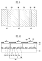
- FIG. 1A is a plan view illustrating a method for depositing a thin film according to an embodiment.
- FIG. 1B is a sectional view taken along line I 1 -I 2 of FIG. 1A .
- FIG. 1C is a partial sectional view illustrating a shadow mask.
- FIG. 2 is a sectional view illustrating a method for forming a thin film according to an embodiment.
- FIGS. 3A and 3B are graphs illustrating a logarithmic spiral.
- FIGS. 4 to 7 are sectional views illustrating a method for forming a thin film according to an embodiment.
- FIGS. 8A to 8E are sectional views illustrating a method for fabricating an OLED display according to an embodiment.
- FIG. 9 is a plan view illustrating a method for fabricating an OLED display according to an embodiment.
- FIG. 10 is a sectional view illustrating a method for fabricating an OLED display according to another embodiment.
- FIG. 11 is a flowchart illustrating an exemplary procedure for forming a thin film according to an embodiment.
- a plurality of shadow masks 20 are formed on a substrate 10 .
- the substrate 10 may be formed of at least one of glass, polymer, metal or silicon, or one or more compounds thereof.
- the substrate 10 preferably has flexibility.
- the shadow masks 20 are arranged in row and column directions.
- the shadow masks 20 arranged in the column directions are connected to each other to form a stripe shape and the shadow masks 20 may be spaced apart from each other at regular intervals.
- the shadow masks 20 extend in the column direction and are substantially equally spaced apart from each other in the row direction.
- the shadow mask 20 is formed in an asymmetric structure including a vertex 22 positioned on a vertical line VL which is perpendicular with respect to a surface of the substrate 10 , a first side 24 forming an acute angle with the surface of the substrate 10 , and a second side 26 connected to the surface of the substrate 10 and the first side 24 through the vertex 22 .
- the length of the first side 24 is the radius of the curvature of the second side 26 .
- the vertex 22 may be positioned on the line connecting the surface of the substrate 10 and a deposition source.
- the first and second sides 24 and 26 may be formed to have a curved surface.
- the first side 24 may be formed as a planar surface and the second side 26 may be formed to have a curved surface.
- the shadow masks 20 may be formed of an inorganic or organic electrically insulating material.
- the shadow masks 20 may be formed by sequentially forming an insulating layer and a photoresist layer on the substrate 10 , patterning the photoresist layer through a lithography and development process, and then patterning the insulating layer through a dry etching process using the patterned photoresist layer as a mask.
- the substrate 10 is bent and then fixed so that the surface of the substrate 10 has a predetermined curvature.
- the curvature of the surface of the substrate 10 corresponds to a logarithmic spiral.
- Equation 1 when the polar coordinate using zero as a starting point (definite point or pole) is (r, ⁇ ), the logarithmic spiral may be defined as shown in the following Equation 1 or 2.
- e is the base of the natural logarithm
- a is an arbitrary real constant
- b is cot ⁇ .
- Equation 1 or 2 if a and b are real numbers, the curved line is defined as shown in the following Equations 3 and 4.
- the logarithmic spiral has a characteristic in which the angle ( 100 ) between the tangent and the radial line is constant at each coordinate (r, ⁇ ).
- the logarithmic spiral LS is a spiral obtained by cutting all straight lines starting from the starting point.
- ⁇ is a constant
- the angle between the straight line and the spiral is constant in all sections (e.g., portion A).
- a deposition source 30 is disposed at a position having substantially equal angles with respect to central and peripheral portions of the substrate 10 .
- the deposition source is positioned at the starting point or pole of the logarithmic spiral defined by the substrate 10 .
- the central and peripheral portions are arbitrary positions and the peripheral portion may include all positions from the central portion to an edge portion. That is, the central and peripheral portions of the substrate 10 may refer to the entire surface of the substrate 10 .
- a radial line originating from the deposition source 10 forms a substantially equal angle with respect to each position of the substrate 10 .
- the equal angles are angles ⁇ 1 , ⁇ 2 , and ⁇ 3 between lines perpendicular to the surface of the substrate 10 , e.g., a vertical line VL 2 at the central portion of the substrate 10 and vertical lines VL 1 and VL 3 at the peripheral portions of the substrate 10 , and lines L 1 , L 2 and L 3 connecting the surface of the substrate 10 , the vertices 22 of the shadow masks 20 , and the deposition source 30 .
- the angles ⁇ 1 , ⁇ 2 , and ⁇ 3 are substantially equal to one another.
- the equal angles may be between about 1 to about 45 degrees.
- the deposition source 30 may be located such that the center axis of the deposition source is substantially parallel to the normal N of the central portion of the substrate 10 .
- the substrate 10 may be fixed to a substrate support 40 having a surface 42 with a curvature having a logarithmic spiral corresponding to that of the substrate 10 .
- a substrate support 50 is formed into a symmetric structure in which surfaces 52 a and 52 b have symmetric curvatures and two substrates 10 may be respectively fixed to the surfaces 52 a and 52 b with the symmetric structure.
- the deposition source 30 is disposed at a position having an equal angle with respect to each of the central and peripheral portions of each substrate 10 .
- a thin film can be simultaneously deposited on the two substrates 10 through a single deposition process.
- a thin film 60 is deposited on the substrate 10 including the shadow masks 20 from the deposition source 30 .
- the deposition source 30 may be configured to evaporate, vaporize or sublimate a deposition material, or may be configured as a sputtering device.
- An open mask 70 may be disposed above the substrate 10 so that the thin film 60 can be deposited in only a desired area. Since an opening 70 a is formed in the open mask 70 so that a predetermined area of the substrate 10 including the plurality of shadow masks 20 is exposed, the thin film 60 can be deposited in only the area exposed by the opening 70 a.
- the open mask 70 is preferably curved to have a curvature similar to that of the substrate 10 , so that the distance between the substrate 10 and the open mask 70 is constant.
- a conducting material or metal material is used as a deposition material in a crucible of the deposition source 30 and the crucible is heated using a heater, the material is evaporated, vaporized or sublimated in the direction of the substrate 10 , thereby depositing the thin film 60 .
- the surface of the substrate 10 adjacent to the first sides 24 of the shadow masks 20 , becomes a shadow area SA with respect to the deposition source 30 , and hence the thin film is not deposited in the shadow area SA.
- the shadow area SA provides a distance spaced between the thin films 60 . Since the deposition source 30 is disposed at a position having equal angles with respect to the central and peripheral portions of the substrate 10 , the positions and sizes of the shadow areas SA at the central and peripheral portions of the substrate 10 are substantially uniform.
- the size of the shadow area SA i.e., the distance between the thin films 60 may be determined by the height of the shadow mask 20 and the angles ⁇ 1 , ⁇ 2 , and ⁇ 3 .
- the thin film 60 can be deposited to have a substantially uniform thickness. Since the positions and sizes of the shadow areas SA are substantially uniform, the thin film can be formed to have substantially a uniform width and spacing.
- the thin film 60 may be used as an electrode or wire.
- the thin film 60 may be applied in forming an electrode of an organic light-emitting diode (OLED) constituting a display unit of an OLED display or in forming a sensing electrode of a touch screen, etc.
- OLED organic light-emitting diode
- FIGS. 8A to 8E are sectional views illustrating a method for fabricating an OLED display according to an embodiment.
- a plurality of first electrodes 120 are formed on a substrate 100 .
- the substrate 100 may be formed of at least one of glass, polymer, metal or silicon, or one or more compounds thereof.
- the substrate 100 preferably has flexibility.
- the first electrode 120 is, for example, an anode electrode of an OLED and may be formed of a transparent conductive material such as indium tin oxide (ITO) or indium zinc oxide (IZO), a metal such as chrome (Cr), gold (Au), silver (Ag), or aluminum (Al), or an alloy thereof.
- a transparent conductive material such as indium tin oxide (ITO) or indium zinc oxide (IZO)
- a metal such as chrome (Cr), gold (Au), silver (Ag), or aluminum (Al), or an alloy thereof.
- insulating layers 140 are formed on the substrate 100 including the first electrodes 120 .
- the insulating layer 140 is patterned so that an emission area of the first electrode 120 is exposed.
- the insulating layer 140 is a pixel defining layer for defining pixels and electrically insulating the pixels.
- the insulating layer 140 may be formed of an organic material such as acryl resin or polyimide resin, or an inorganic material such as silicon oxide (SiO 2 ), titanium oxide (TiO 2 ), or silicon nitride (SiN x ).
- an organic thin film layer 160 is formed on the exposed first electrode 120 .
- the organic thin film layer 160 includes a hole injection layer, an emission layer and an electron injection layer.
- the organic thin film layer 160 may further include a hole transport layer and an electron transport layer.
- the emission layer generally includes at least one materials which can emit red, green, blue, or white light.
- a shadow mask 180 is formed on the insulating layer 140 .
- the shadow mask 180 may be formed of an inorganic or organic material.
- the shadow mask 180 may be formed by depositing an inorganic or organic insulating material on the substrate 100 and patterning an insulating layer through a lithography and dry etching process using a photoresist layer.
- the shadow mask 180 is formed into an asymmetric structure including a vertex 22 , a first side 24 , and a second side 26 .
- a plurality of shadow masks 180 formed on the respective insulating layers 140 are necessarily spaced apart from each other at an equal interval.
- the substrate 100 having the shadow masks 180 formed thereon is bent and then fixed so that the surface of the substrate 100 has a predetermined curvature.
- the substrate 100 may be fixed to the substrate support 40 or 50 shown in FIG. 5 or 6 .
- a deposition source 30 is disposed at a position having an equal angle with respect to each of the central and peripheral portions of the substrate 100 .
- a thin film is deposited on the shadow mask 180 and the organic thin film layer 160 from the deposition source 30 , thereby forming second electrodes 200 .
- the second electrode 200 is a cathode electrode of the OLED and may be formed of a metal such as Al or Ag.
- FIG. 9 is a plan view of FIG. 8D .
- the deposition source is disposed at the position having an equal angle with respect to each of the central and peripheral portions of the substrate 100 . Since the surface of the substrate 100 is curved to have a constant curvature with respect to the deposition source, the second electrodes 200 can be formed to have a substantially uniform thickness over the entire substrate 100 . Since the thin film is not deposited in a shadow area formed by the shadow mask 180 , the second electrode 200 may be formed with a constant width at a constant interval.
- the second electrodes 200 are formed to have a stripe shape.
- One of the sides of the second electrodes 200 may be connected to each other when necessary.
- the second electrodes 200 may be used as sensing electrodes of an in-cell type touch screen.
- the second electrodes 200 Since the thickness and width of the second electrodes 200 are constant, the second electrodes 200 have substantially the same self-resistance value. Since the spacing between the second electrodes 200 is also constant, the signal-to-noise ratio is excellent due to substantially uniform parasitic capacitance.
- FIG. 10 is a sectional view illustrating a method for fabricating an OLED display according to another embodiment.
- a device forming layer 300 may be formed on a substrate 100 .
- the device forming layer 300 may include a thin film transistor T for transmitting a signal to an OLED, a capacitor C for maintaining the signal, and an insulating layer 320 formed on the substrate 100 including the thin film transistor T and the capacitor C.
- the thin film transistor T includes a gate electrode 312 formed on the substrate 100 , a semiconductor layer 316 disposed above the gate electrode 312 and electrically insulated from the gate electrode 312 by an insulating layer 314 , and source and drain electrodes 318 respectively connected to source and drain areas of the semiconductor layer 316 .
- the capacitor C is formed on the substrate 100 adjacent to the thin film transistor T.
- the capacitor C may be formed into a laminated structure of a lower electrode 312 a, the insulating layer 314 , and an upper electrode 318 a.
- a first electrode 120 of the OLED is formed on the device forming layer 300 configured as described above and is connected to the source or drain electrode 318 of the thin film transistor T.
- the first electrode 120 may be connected to the source or drain electrode 318 of the thin film transistor T through a via hole of the insulating layer 320 formed between the thin film transistor T and the first electrode 120 .
- the OLED is completed by sequentially forming an organic thin film layer and a second electrode.
- FIG. 11 is a flowchart showing an exemplary procedure 400 for forming a thin film according to one embodiment.
- additional states may be added, others removed, or the order of the states changed in FIG. 4 .
- state 410 shadow masks are formed on a substrate.
- state 420 the substrate is bent to a predetermined curvature.
- the predetermined curvature may be a logarithmic curvature.
- state 430 a deposition source is placed to form an equal angle with respect to central and peripheral portions of the substrate. The equal angle may be formed with respect to each point of the substrate.
- the thin film is formed on the substrate by deposition.
- a conductive layer was deposited on a substrate and then patterned through lithography and etching processes using a photoresist layer.
- the lithography process is a process of forming a photoresist pattern through exposure and development processes using a mask and the etching process is a process of etching the conductive layer into a predetermined pattern, using the photoresist pattern.
- a substrate is bent and then fixed to have a predetermined curvature and a deposition source is positioned at a position having an equal angle with respect to each of central and peripheral portions of the substrate.
- shadow masks are formed so that shadow areas with a constant size are formed at positions having a constant angle with respect to the deposition source. Since each of the central and peripheral portions of the substrate are positioned to have the equal angle with respect to the deposition source, a thin film can be deposited to have a substantially uniform thickness. Since the positions and sizes of the shadow areas are uniform, electrodes or wires with substantially uniform width and spacing can be formed.
- the number of processes and the time taken to perform the processes is decreased when compared with typical processes, so that it is possible to reduce the manufacturing cost and increase the yield.
- the electrode of the OLED can be used as a sensing electrode of a touch screen.
- the electrode of the OLED can be used as a sensing electrode of a touch screen.
Abstract
Description
r=aebθ Equation 1
θ=(1/b)In(r/a), Equation 2
r=aebθ Equation 1
θ=(1/b)In(r/a), Equation 2
r=aebθ Equation 1
θ=(1/b)In(r/a) Equation 2
x(t)=r(t)cos(t)=ae bθcos(t) Equation 3
y(t)=r(t)sin(t)=ae bθsin(t) Equation 4
Claims (29)
r=aebθ Equation 1
θ=(1/b)In(r/a), Equation 2
r=ae bθ Equation 1
θ=(1/b)In(r/a), Equation 2
Applications Claiming Priority (2)
| Application Number | Priority Date | Filing Date | Title |
|---|---|---|---|
| KR10-2013-0111497 | 2013-09-17 | ||
| KR20130111497A KR20150031819A (en) | 2013-09-17 | 2013-09-17 | Method for depositing thin film and method for fabricating organic light emitting display device using the same |
Publications (2)
| Publication Number | Publication Date |
|---|---|
| US20150079711A1 US20150079711A1 (en) | 2015-03-19 |
| US9614192B2 true US9614192B2 (en) | 2017-04-04 |
Family
ID=52668294
Family Applications (1)
| Application Number | Title | Priority Date | Filing Date |
|---|---|---|---|
| US14/487,946 Expired - Fee Related US9614192B2 (en) | 2013-09-17 | 2014-09-16 | Method for forming thin film and method for fabricating organic light-emitting diode (OLED) display using the same |
Country Status (2)
| Country | Link |
|---|---|
| US (1) | US9614192B2 (en) |
| KR (1) | KR20150031819A (en) |
Cited By (1)
| Publication number | Priority date | Publication date | Assignee | Title |
|---|---|---|---|---|
| US11196002B2 (en) * | 2016-10-06 | 2021-12-07 | Dai Nippon Printing Co., Ltd. | Method for producing vapor deposition mask, method for producing organic semiconductor element, and method for producing organic EL display |
Families Citing this family (1)
| Publication number | Priority date | Publication date | Assignee | Title |
|---|---|---|---|---|
| KR20140061808A (en) * | 2012-11-14 | 2014-05-22 | 삼성디스플레이 주식회사 | Apparatus for depositing organic material |
Citations (11)
| Publication number | Priority date | Publication date | Assignee | Title |
|---|---|---|---|---|
| US5294870A (en) | 1991-12-30 | 1994-03-15 | Eastman Kodak Company | Organic electroluminescent multicolor image display device |
| US5294869A (en) * | 1991-12-30 | 1994-03-15 | Eastman Kodak Company | Organic electroluminescent multicolor image display device |
| US6255775B1 (en) * | 1997-05-15 | 2001-07-03 | Nec Corporation | Shadow mask, a method of manufacturing a color thin film electroluminescent display apparatus using the shadow mask, and a color thin film electroluminescent display apparatus |
| US6965198B2 (en) * | 2001-06-21 | 2005-11-15 | 3M Innovative Properties Company | Organic light emitting full color display panel |
| US7093937B2 (en) * | 2001-09-17 | 2006-08-22 | Carl Zeiss Smt Ag | Optical component and coating system for coating substrates for optical components |
| US20070072337A1 (en) * | 2005-09-27 | 2007-03-29 | Hitachi Displays, Ltd. | Method of manufacturing the organic electroluminescent display and organic electroluminescent display manufactured by the method |
| US20070072128A1 (en) * | 2005-09-28 | 2007-03-29 | Frank Miceli | Method of manufacturing an integrated circuit to obtain uniform exposure in a photolithographic process |
| KR20100084655A (en) | 2008-08-15 | 2010-07-27 | 신크론 컴퍼니 리미티드 | Optical thin film deposition device and optical thin film fabrication method |
| US20120100644A1 (en) * | 2010-10-22 | 2012-04-26 | Valeriy Prushinskiy | Organic layer deposition apparatus, and method of manufacturing organic light-emitting display apparatus using the same |
| US20140191201A1 (en) * | 2013-01-08 | 2014-07-10 | OLEDWorks LLC | Apparatus and Method for Making OLED Lighting Device |
| US9172064B2 (en) * | 2012-06-13 | 2015-10-27 | Samsung Display Co., Ltd. | Mask for deposition and method for manufacturing organic light emitting diode display using the same |
-
2013
- 2013-09-17 KR KR20130111497A patent/KR20150031819A/en not_active Application Discontinuation
-
2014
- 2014-09-16 US US14/487,946 patent/US9614192B2/en not_active Expired - Fee Related
Patent Citations (13)
| Publication number | Priority date | Publication date | Assignee | Title |
|---|---|---|---|---|
| US5294870A (en) | 1991-12-30 | 1994-03-15 | Eastman Kodak Company | Organic electroluminescent multicolor image display device |
| US5294869A (en) * | 1991-12-30 | 1994-03-15 | Eastman Kodak Company | Organic electroluminescent multicolor image display device |
| US6255775B1 (en) * | 1997-05-15 | 2001-07-03 | Nec Corporation | Shadow mask, a method of manufacturing a color thin film electroluminescent display apparatus using the shadow mask, and a color thin film electroluminescent display apparatus |
| US6965198B2 (en) * | 2001-06-21 | 2005-11-15 | 3M Innovative Properties Company | Organic light emitting full color display panel |
| US7093937B2 (en) * | 2001-09-17 | 2006-08-22 | Carl Zeiss Smt Ag | Optical component and coating system for coating substrates for optical components |
| US20070072337A1 (en) * | 2005-09-27 | 2007-03-29 | Hitachi Displays, Ltd. | Method of manufacturing the organic electroluminescent display and organic electroluminescent display manufactured by the method |
| US20070072128A1 (en) * | 2005-09-28 | 2007-03-29 | Frank Miceli | Method of manufacturing an integrated circuit to obtain uniform exposure in a photolithographic process |
| KR20100084655A (en) | 2008-08-15 | 2010-07-27 | 신크론 컴퍼니 리미티드 | Optical thin film deposition device and optical thin film fabrication method |
| US20110151135A1 (en) * | 2008-08-15 | 2011-06-23 | Ekishu Nagae | Optical thin-film deposition device and optical thin-film fabrication method |
| US20120100644A1 (en) * | 2010-10-22 | 2012-04-26 | Valeriy Prushinskiy | Organic layer deposition apparatus, and method of manufacturing organic light-emitting display apparatus using the same |
| KR20120042153A (en) | 2010-10-22 | 2012-05-03 | 삼성모바일디스플레이주식회사 | Apparatus for organic layer deposition, method for manufacturing of organic light emitting display apparatus using the same |
| US9172064B2 (en) * | 2012-06-13 | 2015-10-27 | Samsung Display Co., Ltd. | Mask for deposition and method for manufacturing organic light emitting diode display using the same |
| US20140191201A1 (en) * | 2013-01-08 | 2014-07-10 | OLEDWorks LLC | Apparatus and Method for Making OLED Lighting Device |
Cited By (1)
| Publication number | Priority date | Publication date | Assignee | Title |
|---|---|---|---|---|
| US11196002B2 (en) * | 2016-10-06 | 2021-12-07 | Dai Nippon Printing Co., Ltd. | Method for producing vapor deposition mask, method for producing organic semiconductor element, and method for producing organic EL display |
Also Published As
| Publication number | Publication date |
|---|---|
| US20150079711A1 (en) | 2015-03-19 |
| KR20150031819A (en) | 2015-03-25 |
Similar Documents
| Publication | Publication Date | Title |
|---|---|---|
| US11950490B2 (en) | Display device having conductive spacers connecting anode and cathode on opposing substrates | |
| US11251410B2 (en) | Flexible display substrate and method for manufacturing the same | |
| CN114097102B (en) | Optoelectronic device comprising a light transmissive region having light diffraction features | |
| CN107170758B (en) | Flexible display substrate, manufacturing method thereof and display device | |
| CN108598122B (en) | Display substrate, manufacturing method thereof and display device | |
| KR101801349B1 (en) | Organic light emitting display apparatus and manufacturing method thereof | |
| US10665793B2 (en) | Pixel definition layer having an incline for an organic light emitting device | |
| CN110416269B (en) | Display panel and manufacturing method thereof | |
| JP6257964B2 (en) | Organic light emitting diode, touch display, and manufacturing method thereof | |
| WO2020200168A1 (en) | Amoled display screen, display device and mobile terminal | |
| US10788907B2 (en) | Touch display substrate, fabrication method and touch display device | |
| US20180219163A1 (en) | Flexible Array Substrate, the Preparation Method Thereof, and Flexible Display Device | |
| WO2019037520A1 (en) | Display substrate and display apparatus | |
| US11374173B2 (en) | Evaporation mask, OLED panel and system, and evaporation monitoring method | |
| TWI557894B (en) | Organic light-emitting display device and method of manufacturing the same | |
| US11340745B2 (en) | Touch structure and method for manufacturing the same, touch substrate and touch display device | |
| CN106856203B (en) | Top-emitting display light-emitting device and preparation method thereof | |
| CN112470287A (en) | Display substrate and related device | |
| US20180053718A1 (en) | Layer stacking structure, array substrate and display device | |
| WO2018099079A1 (en) | Array substrate and display device | |
| CN112420784A (en) | Array substrate, preparation method thereof and display panel | |
| JP2016201257A (en) | Method of manufacturing display device | |
| US9614192B2 (en) | Method for forming thin film and method for fabricating organic light-emitting diode (OLED) display using the same | |
| CN110828483A (en) | Top-emitting OLED display back plate, manufacturing method thereof and OLED display device | |
| WO2020233485A1 (en) | Light-emitting component, manufacturing method therefor, mask, and display device |
Legal Events
| Date | Code | Title | Description |
|---|---|---|---|
| AS | Assignment |
Owner name: SAMSUNG DISPLAY CO., LTD., KOREA, REPUBLIC OF Free format text: ASSIGNMENT OF ASSIGNORS INTEREST;ASSIGNORS:KAPLAN, LEONID;PRUSHINSKIY, VALERIY;LEE, WON-BAEK;AND OTHERS;SIGNING DATES FROM 20140912 TO 20140916;REEL/FRAME:033789/0715 |
|
| FEPP | Fee payment procedure |
Free format text: PAYOR NUMBER ASSIGNED (ORIGINAL EVENT CODE: ASPN); ENTITY STATUS OF PATENT OWNER: LARGE ENTITY Free format text: PAYER NUMBER DE-ASSIGNED (ORIGINAL EVENT CODE: RMPN); ENTITY STATUS OF PATENT OWNER: LARGE ENTITY |
|
| FEPP | Fee payment procedure |
Free format text: PAYOR NUMBER ASSIGNED (ORIGINAL EVENT CODE: ASPN); ENTITY STATUS OF PATENT OWNER: LARGE ENTITY |
|
| STCF | Information on status: patent grant |
Free format text: PATENTED CASE |
|
| FEPP | Fee payment procedure |
Free format text: MAINTENANCE FEE REMINDER MAILED (ORIGINAL EVENT CODE: REM.); ENTITY STATUS OF PATENT OWNER: LARGE ENTITY |
|
| LAPS | Lapse for failure to pay maintenance fees |
Free format text: PATENT EXPIRED FOR FAILURE TO PAY MAINTENANCE FEES (ORIGINAL EVENT CODE: EXP.); ENTITY STATUS OF PATENT OWNER: LARGE ENTITY |
|
| STCH | Information on status: patent discontinuation |
Free format text: PATENT EXPIRED DUE TO NONPAYMENT OF MAINTENANCE FEES UNDER 37 CFR 1.362 |
|
| FP | Lapsed due to failure to pay maintenance fee |
Effective date: 20210404 |