US9614182B2 - Method of manufacturing display apparatus that includes using an energy beam to form an encapsulation layer - Google Patents
Method of manufacturing display apparatus that includes using an energy beam to form an encapsulation layer Download PDFInfo
- Publication number
- US9614182B2 US9614182B2 US14/531,302 US201414531302A US9614182B2 US 9614182 B2 US9614182 B2 US 9614182B2 US 201414531302 A US201414531302 A US 201414531302A US 9614182 B2 US9614182 B2 US 9614182B2
- Authority
- US
- United States
- Prior art keywords
- thin
- encapsulation layer
- film encapsulation
- display device
- energy beam
- Prior art date
- Legal status (The legal status is an assumption and is not a legal conclusion. Google has not performed a legal analysis and makes no representation as to the accuracy of the status listed.)
- Expired - Fee Related, expires
Links
- 238000005538 encapsulation Methods 0.000 title claims abstract description 102
- 238000004519 manufacturing process Methods 0.000 title claims abstract description 28
- 239000010409 thin film Substances 0.000 claims abstract description 99
- 238000000034 method Methods 0.000 claims abstract description 58
- 230000001678 irradiating effect Effects 0.000 claims abstract description 52
- 229910010272 inorganic material Inorganic materials 0.000 claims abstract description 50
- 239000011147 inorganic material Substances 0.000 claims abstract description 50
- 239000000758 substrate Substances 0.000 claims abstract description 40
- 230000007704 transition Effects 0.000 claims abstract description 17
- 230000015572 biosynthetic process Effects 0.000 claims abstract description 4
- 239000000463 material Substances 0.000 claims description 84
- 230000008569 process Effects 0.000 claims description 33
- ANOBYBYXJXCGBS-UHFFFAOYSA-L stannous fluoride Chemical compound F[Sn]F ANOBYBYXJXCGBS-UHFFFAOYSA-L 0.000 claims description 28
- 239000007789 gas Substances 0.000 claims description 14
- 238000010884 ion-beam technique Methods 0.000 claims description 13
- 229910000149 boron phosphate Inorganic materials 0.000 claims description 12
- 238000010894 electron beam technology Methods 0.000 claims description 12
- XOLBLPGZBRYERU-UHFFFAOYSA-N tin dioxide Chemical compound O=[Sn]=O XOLBLPGZBRYERU-UHFFFAOYSA-N 0.000 claims description 12
- XLOMVQKBTHCTTD-UHFFFAOYSA-N Zinc monoxide Chemical compound [Zn]=O XLOMVQKBTHCTTD-UHFFFAOYSA-N 0.000 claims description 11
- YZYDPPZYDIRSJT-UHFFFAOYSA-K boron phosphate Chemical compound [B+3].[O-]P([O-])([O-])=O YZYDPPZYDIRSJT-UHFFFAOYSA-K 0.000 claims description 11
- 238000001816 cooling Methods 0.000 claims description 10
- 238000000151 deposition Methods 0.000 claims description 9
- JKWMSGQKBLHBQQ-UHFFFAOYSA-N diboron trioxide Chemical compound O=BOB=O JKWMSGQKBLHBQQ-UHFFFAOYSA-N 0.000 claims description 9
- 230000002093 peripheral effect Effects 0.000 claims description 9
- 229910001887 tin oxide Inorganic materials 0.000 claims description 8
- IJGRMHOSHXDMSA-UHFFFAOYSA-N Atomic nitrogen Chemical compound N#N IJGRMHOSHXDMSA-UHFFFAOYSA-N 0.000 claims description 7
- 229910052782 aluminium Inorganic materials 0.000 claims description 6
- 230000008021 deposition Effects 0.000 claims description 6
- QVGXLLKOCUKJST-UHFFFAOYSA-N atomic oxygen Chemical compound [O] QVGXLLKOCUKJST-UHFFFAOYSA-N 0.000 claims description 5
- 229910052760 oxygen Inorganic materials 0.000 claims description 5
- 239000001301 oxygen Substances 0.000 claims description 5
- 229910052799 carbon Inorganic materials 0.000 claims description 4
- 239000011261 inert gas Substances 0.000 claims description 4
- 229910000484 niobium oxide Inorganic materials 0.000 claims description 4
- URLJKFSTXLNXLG-UHFFFAOYSA-N niobium(5+);oxygen(2-) Chemical compound [O-2].[O-2].[O-2].[O-2].[O-2].[Nb+5].[Nb+5] URLJKFSTXLNXLG-UHFFFAOYSA-N 0.000 claims description 4
- QGLKJKCYBOYXKC-UHFFFAOYSA-N nonaoxidotritungsten Chemical compound O=[W]1(=O)O[W](=O)(=O)O[W](=O)(=O)O1 QGLKJKCYBOYXKC-UHFFFAOYSA-N 0.000 claims description 4
- 229910001392 phosphorus oxide Inorganic materials 0.000 claims description 4
- VSAISIQCTGDGPU-UHFFFAOYSA-N tetraphosphorus hexaoxide Chemical compound O1P(O2)OP3OP1OP2O3 VSAISIQCTGDGPU-UHFFFAOYSA-N 0.000 claims description 4
- YUOWTJMRMWQJDA-UHFFFAOYSA-J tin(iv) fluoride Chemical compound [F-].[F-].[F-].[F-].[Sn+4] YUOWTJMRMWQJDA-UHFFFAOYSA-J 0.000 claims description 4
- 229910001930 tungsten oxide Inorganic materials 0.000 claims description 4
- XAGFODPZIPBFFR-UHFFFAOYSA-N aluminium Chemical compound [Al] XAGFODPZIPBFFR-UHFFFAOYSA-N 0.000 claims description 3
- 230000008020 evaporation Effects 0.000 claims description 3
- 238000001704 evaporation Methods 0.000 claims description 3
- 229910052757 nitrogen Inorganic materials 0.000 claims description 3
- 238000005507 spraying Methods 0.000 claims description 3
- 238000004544 sputter deposition Methods 0.000 claims description 3
- 238000002207 thermal evaporation Methods 0.000 claims description 3
- OKTJSMMVPCPJKN-UHFFFAOYSA-N Carbon Chemical compound [C] OKTJSMMVPCPJKN-UHFFFAOYSA-N 0.000 claims description 2
- 238000005137 deposition process Methods 0.000 claims description 2
- 238000000313 electron-beam-induced deposition Methods 0.000 claims description 2
- 229910011255 B2O3 Inorganic materials 0.000 claims 1
- 239000010410 layer Substances 0.000 description 138
- 238000004925 denaturation Methods 0.000 description 16
- 230000036425 denaturation Effects 0.000 description 16
- -1 region Substances 0.000 description 14
- 230000007547 defect Effects 0.000 description 10
- 238000010586 diagram Methods 0.000 description 8
- 238000002411 thermogravimetry Methods 0.000 description 6
- 230000009477 glass transition Effects 0.000 description 5
- 239000012535 impurity Substances 0.000 description 5
- BASFCYQUMIYNBI-UHFFFAOYSA-N platinum Chemical compound [Pt] BASFCYQUMIYNBI-UHFFFAOYSA-N 0.000 description 5
- PXHVJJICTQNCMI-UHFFFAOYSA-N Nickel Chemical compound [Ni] PXHVJJICTQNCMI-UHFFFAOYSA-N 0.000 description 4
- KDLHZDBZIXYQEI-UHFFFAOYSA-N Palladium Chemical compound [Pd] KDLHZDBZIXYQEI-UHFFFAOYSA-N 0.000 description 4
- VYPSYNLAJGMNEJ-UHFFFAOYSA-N Silicium dioxide Chemical compound O=[Si]=O VYPSYNLAJGMNEJ-UHFFFAOYSA-N 0.000 description 4
- 150000001875 compounds Chemical class 0.000 description 4
- 230000035876 healing Effects 0.000 description 4
- 239000000203 mixture Substances 0.000 description 4
- 230000000149 penetrating effect Effects 0.000 description 4
- 239000011787 zinc oxide Substances 0.000 description 4
- 239000011575 calcium Substances 0.000 description 3
- 239000011651 chromium Substances 0.000 description 3
- 238000000113 differential scanning calorimetry Methods 0.000 description 3
- 239000010931 gold Substances 0.000 description 3
- 229910003437 indium oxide Inorganic materials 0.000 description 3
- PJXISJQVUVHSOJ-UHFFFAOYSA-N indium(iii) oxide Chemical compound [O-2].[O-2].[O-2].[In+3].[In+3] PJXISJQVUVHSOJ-UHFFFAOYSA-N 0.000 description 3
- 239000011777 magnesium Substances 0.000 description 3
- 239000011368 organic material Substances 0.000 description 3
- 229910052779 Neodymium Inorganic materials 0.000 description 2
- 230000004888 barrier function Effects 0.000 description 2
- 239000003990 capacitor Substances 0.000 description 2
- 238000006243 chemical reaction Methods 0.000 description 2
- 229910052804 chromium Inorganic materials 0.000 description 2
- 239000010419 fine particle Substances 0.000 description 2
- 229910052737 gold Inorganic materials 0.000 description 2
- 238000002347 injection Methods 0.000 description 2
- 239000007924 injection Substances 0.000 description 2
- 229910052741 iridium Inorganic materials 0.000 description 2
- 229910052744 lithium Inorganic materials 0.000 description 2
- 229910052749 magnesium Inorganic materials 0.000 description 2
- 229910052759 nickel Inorganic materials 0.000 description 2
- 229910052763 palladium Inorganic materials 0.000 description 2
- 229910052697 platinum Inorganic materials 0.000 description 2
- 239000000377 silicon dioxide Substances 0.000 description 2
- 229910052709 silver Inorganic materials 0.000 description 2
- 239000002356 single layer Substances 0.000 description 2
- OYPRJOBELJOOCE-UHFFFAOYSA-N Calcium Chemical compound [Ca] OYPRJOBELJOOCE-UHFFFAOYSA-N 0.000 description 1
- VYZAMTAEIAYCRO-UHFFFAOYSA-N Chromium Chemical compound [Cr] VYZAMTAEIAYCRO-UHFFFAOYSA-N 0.000 description 1
- MYMOFIZGZYHOMD-UHFFFAOYSA-N Dioxygen Chemical compound O=O MYMOFIZGZYHOMD-UHFFFAOYSA-N 0.000 description 1
- WHXSMMKQMYFTQS-UHFFFAOYSA-N Lithium Chemical compound [Li] WHXSMMKQMYFTQS-UHFFFAOYSA-N 0.000 description 1
- FYYHWMGAXLPEAU-UHFFFAOYSA-N Magnesium Chemical compound [Mg] FYYHWMGAXLPEAU-UHFFFAOYSA-N 0.000 description 1
- BQCADISMDOOEFD-UHFFFAOYSA-N Silver Chemical compound [Ag] BQCADISMDOOEFD-UHFFFAOYSA-N 0.000 description 1
- 229910052769 Ytterbium Inorganic materials 0.000 description 1
- 230000001154 acute effect Effects 0.000 description 1
- 239000012298 atmosphere Substances 0.000 description 1
- 229910052791 calcium Inorganic materials 0.000 description 1
- 230000008859 change Effects 0.000 description 1
- 238000000354 decomposition reaction Methods 0.000 description 1
- 229910001873 dinitrogen Inorganic materials 0.000 description 1
- 229910001882 dioxygen Inorganic materials 0.000 description 1
- 239000010408 film Substances 0.000 description 1
- 230000014509 gene expression Effects 0.000 description 1
- 239000011521 glass Substances 0.000 description 1
- PCHJSUWPFVWCPO-UHFFFAOYSA-N gold Chemical compound [Au] PCHJSUWPFVWCPO-UHFFFAOYSA-N 0.000 description 1
- 230000005525 hole transport Effects 0.000 description 1
- AMGQUBHHOARCQH-UHFFFAOYSA-N indium;oxotin Chemical compound [In].[Sn]=O AMGQUBHHOARCQH-UHFFFAOYSA-N 0.000 description 1
- 239000011810 insulating material Substances 0.000 description 1
- GKOZUEZYRPOHIO-UHFFFAOYSA-N iridium atom Chemical compound [Ir] GKOZUEZYRPOHIO-UHFFFAOYSA-N 0.000 description 1
- 239000007788 liquid Substances 0.000 description 1
- 239000004973 liquid crystal related substance Substances 0.000 description 1
- 230000007257 malfunction Effects 0.000 description 1
- 229910052751 metal Inorganic materials 0.000 description 1
- 239000002184 metal Substances 0.000 description 1
- 150000002739 metals Chemical class 0.000 description 1
- QEFYFXOXNSNQGX-UHFFFAOYSA-N neodymium atom Chemical compound [Nd] QEFYFXOXNSNQGX-UHFFFAOYSA-N 0.000 description 1
- 239000012299 nitrogen atmosphere Substances 0.000 description 1
- 238000013021 overheating Methods 0.000 description 1
- 238000007254 oxidation reaction Methods 0.000 description 1
- 239000002245 particle Substances 0.000 description 1
- 230000035515 penetration Effects 0.000 description 1
- 230000009257 reactivity Effects 0.000 description 1
- 235000012239 silicon dioxide Nutrition 0.000 description 1
- 239000004332 silver Substances 0.000 description 1
- 239000007787 solid Substances 0.000 description 1
- 238000002076 thermal analysis method Methods 0.000 description 1
- NAWDYIZEMPQZHO-UHFFFAOYSA-N ytterbium Chemical compound [Yb] NAWDYIZEMPQZHO-UHFFFAOYSA-N 0.000 description 1
- YVTHLONGBIQYBO-UHFFFAOYSA-N zinc indium(3+) oxygen(2-) Chemical compound [O--].[Zn++].[In+3] YVTHLONGBIQYBO-UHFFFAOYSA-N 0.000 description 1
Images


Classifications
-
- H01L51/5253—
-
- C—CHEMISTRY; METALLURGY
- C23—COATING METALLIC MATERIAL; COATING MATERIAL WITH METALLIC MATERIAL; CHEMICAL SURFACE TREATMENT; DIFFUSION TREATMENT OF METALLIC MATERIAL; COATING BY VACUUM EVAPORATION, BY SPUTTERING, BY ION IMPLANTATION OR BY CHEMICAL VAPOUR DEPOSITION, IN GENERAL; INHIBITING CORROSION OF METALLIC MATERIAL OR INCRUSTATION IN GENERAL
- C23C—COATING METALLIC MATERIAL; COATING MATERIAL WITH METALLIC MATERIAL; SURFACE TREATMENT OF METALLIC MATERIAL BY DIFFUSION INTO THE SURFACE, BY CHEMICAL CONVERSION OR SUBSTITUTION; COATING BY VACUUM EVAPORATION, BY SPUTTERING, BY ION IMPLANTATION OR BY CHEMICAL VAPOUR DEPOSITION, IN GENERAL
- C23C14/00—Coating by vacuum evaporation, by sputtering or by ion implantation of the coating forming material
- C23C14/22—Coating by vacuum evaporation, by sputtering or by ion implantation of the coating forming material characterised by the process of coating
-
- H—ELECTRICITY
- H10—SEMICONDUCTOR DEVICES; ELECTRIC SOLID-STATE DEVICES NOT OTHERWISE PROVIDED FOR
- H10K—ORGANIC ELECTRIC SOLID-STATE DEVICES
- H10K50/00—Organic light-emitting devices
- H10K50/80—Constructional details
- H10K50/84—Passivation; Containers; Encapsulations
- H10K50/844—Encapsulations
-
- H—ELECTRICITY
- H10—SEMICONDUCTOR DEVICES; ELECTRIC SOLID-STATE DEVICES NOT OTHERWISE PROVIDED FOR
- H10K—ORGANIC ELECTRIC SOLID-STATE DEVICES
- H10K59/00—Integrated devices, or assemblies of multiple devices, comprising at least one organic light-emitting element covered by group H10K50/00
- H10K59/80—Constructional details
- H10K59/87—Passivation; Containers; Encapsulations
- H10K59/873—Encapsulations
-
- H01L2251/306—
-
- H—ELECTRICITY
- H10—SEMICONDUCTOR DEVICES; ELECTRIC SOLID-STATE DEVICES NOT OTHERWISE PROVIDED FOR
- H10K—ORGANIC ELECTRIC SOLID-STATE DEVICES
- H10K2102/00—Constructional details relating to the organic devices covered by this subclass
- H10K2102/10—Transparent electrodes, e.g. using graphene
- H10K2102/101—Transparent electrodes, e.g. using graphene comprising transparent conductive oxides [TCO]
- H10K2102/102—Transparent electrodes, e.g. using graphene comprising transparent conductive oxides [TCO] comprising tin oxides, e.g. fluorine-doped SnO2
Definitions
- Embodiments relate to a method of manufacturing a display apparatus.
- a display apparatus may include a self-emission display apparatus that consumes a small amount of power and has good view of angles and definition.
- the display apparatus may include a display device that produces an image towards a user, that is arranged between a first electrode and a second electrode, and that includes an organic light-emitting device including at least one emission layer.
- Embodiments are directed to a method of manufacturing a display apparatus.
- the embodiments may be realized by providing a method of manufacturing a display apparatus, the method including forming a display device on a substrate; and forming a thin-film encapsulation layer on the display device, the thin-film encapsulation layer including at least one inorganic layer that includes a low-temperature viscosity transition (LVT) inorganic material, wherein forming the thin-film encapsulation layer includes irradiating an energy beam toward the thin-film encapsulation layer during formation of the thin-film encapsulation layer.
- LVT low-temperature viscosity transition
- Forming the thin-film encapsulation layer may include providing a source material of the thin-film encapsulation layer to the display device.
- Irradiating the energy beam may be simultaneously performed with the providing the source material of the thin-film encapsulation layer to the display device.
- Irradiating the energy beam may include irradiating an energy beam at one or more points of time that overlap a process time for providing the source material of the thin-film encapsulation layer to the display device.
- Irradiating the energy beam may be performed right after providing the source material of the thin-film encapsulation layer to the display device.
- Providing the source material of the thin-film encapsulation layer to the display device may include performing a deposition process.
- Providing the source material of the thin-film encapsulation layer to the display device may include performing at least one selected from the group of evaporation, electron beam deposition, laser deposition, thermal deposition, a spraying method, and a sputtering method.
- Providing the source material of the thin-film encapsulation layer to the display device may include performing co-deposition using the source material of the thin-film encapsulation layer.
- Providing the source material of the thin-film encapsulation layer to the display device may include providing the source material to the display device in a direction that is at an oblique angle relative to a direction to which the energy beam is irradiated to the display device.
- the energy beam may include at least one selected from the group of ion beams, electron beams, laser beams, and neutron beams.
- Irradiating the energy beam may include periodically irradiating the energy beam a plurality of times.
- Irradiating the energy beam may include irregularly irradiating the energy beam a plurality of times.
- Irradiating the energy beam may include ionizing inert gases to provide the energy beam.
- Forming the thin-film encapsulation layer may include cooling the substrate with a cooling member.
- Forming the thin-film encapsulation layer may include injecting a peripheral gas around the substrate.
- the peripheral gas may include oxygen, nitrogen, or an oxynitride gas.
- a viscosity transition temperature of the LVT inorganic material may be a minimum temperature at which fluidity is provided to the LVT inorganic material.
- the LVT inorganic material may include tin oxide.
- the LVT inorganic material may further include one or more of phosphorus oxide, boron phosphate, tin fluoride, niobium oxide, tungsten oxide, aluminum, carbon, ZnO, B 2 O 3 , and BiO.
- the LVT inorganic material may include SnO; SnO and P 2 O 5 ; SnO and BPO 4 ; SnO, SnF 2 , and P 2 O 5 ; SnO, SnF 2 , P 2 O 5 , and NbO; or SnO, SnF 2 , P 2 O 5 , and WO 3 .
- FIG. 1 illustrates a schematic cross-sectional view of a display apparatus manufactured by a method according to an embodiment
- FIGS. 2A through 2D illustrate diagrams of stages in a method of manufacturing a display apparatus, according to an embodiment
- FIGS. 3A through 3E illustrate diagrams of stages in a method of manufacturing a display apparatus, according to another embodiment
- FIG. 4 illustrates a diagram of a stage in a method of manufacturing a display apparatus, according to another embodiment.
- FIG. 5 illustrates a diagram of a stage in a method of manufacturing a display apparatus, according to another embodiment.
- the term “and/or” includes any and all combinations of one or more of the associated listed items. Expressions such as “at least one of,” when preceding a list of elements, modify the entire list of elements and do not modify the individual elements of the list.
- the x-axis, the y-axis, and the z-axis are not limited to three axes of the rectangular coordinate system, and may be interpreted in a broader sense.
- the x-axis, the y-axis, and the z-axis may be perpendicular to one another, or may represent different directions that are not perpendicular to one another.
- a specific process order may be performed differently from the described order.
- two consecutively described processes may be performed substantially at the same time or performed in an order opposite to the described order.
- FIG. 1 illustrates a schematic cross-sectional view of a display apparatus 100 manufactured by a method according to an embodiment.
- the display apparatus 100 may include a substrate 101 , a display device 120 , and a thin-film encapsulation layer 150 .
- the thin-film encapsulation layer 150 may include at least one inorganic layer having low temperature viscosity transition (LVT) inorganic materials.
- LVT low temperature viscosity transition
- the substrate 101 may be formed of various materials.
- the substrate 101 may be formed of transparent glass materials that mainly include silicon dioxide (SiO 2 ).
- the substrate 101 may be formed of a flexible material, e.g., a plastic material.
- the display device 120 may have diverse shapes.
- the display device 120 may be, e.g., an organic light-emitting device or a liquid crystal device (LCD).
- the display device 120 may include various types of devices capable of emitting visible rays towards a user.
- the display device 120 is an organic light-emitting device is described with reference to FIG. 1 .
- the display device 120 may include a first electrode 121 , a second electrode 122 , and an intermediate layer 123 .
- the first electrode 121 may be formed on the substrate 101
- the second electrode 122 may be formed on the first electrode 121
- the intermediate layer 123 may be formed between the first and second electrodes 121 and 122 .
- a buffer layer (not shown) may be further formed between the first electrode 121 and the substrate 101 .
- the buffer layer may provide a planarization layer on the substrate 101 and may help prevent moisture or gas from penetrating into the substrate 101 .
- a barrier layer which may be formed as a single layer or layers that have substantially the same materials as the buffer layer, may be formed between the substrate 101 and the buffer layer.
- the barrier layer may be formed on the substrate 101 and may effectively help prevent moisture from penetrating into the substrate 101 .
- the first electrode 121 may function as an anode, and the second electrode 122 may function as a cathode. In an implementation, polarities of the first and second electrodes 121 and 122 may be changed.
- the first electrode 121 may include, e.g., indium tin oxide (ITO), indium zinc oxide (IZO), zinc oxide (ZnO), indium oxide (In 2 O 3 ), or the like, materials that have high work functions.
- ITO indium tin oxide
- IZO indium zinc oxide
- ZnO zinc oxide
- In 2 O 3 indium oxide
- the first electrode 121 may further include a reflective film formed of, e.g., silver (Ag), magnesium (Mg), aluminum (Al), platinum (Pt), palladium (Pd), gold (Au), nickel (Ni), neodymium (Nd), iridium (Ir), chromium (Cr), lithium (Li), ytterbium (Yb), calcium (Ca), or the like, according to a purpose of using the first electrode 121 and design conditions.
- a reflective film formed of, e.g., silver (Ag), magnesium (Mg), aluminum (Al), platinum (Pt), palladium (Pd), gold (Au), nickel (Ni), neodymium (Nd), iridium (Ir), chromium (Cr), lithium (Li), ytterbium (Yb), calcium (Ca), or the like, according to a purpose of using the first electrode 121 and design conditions.
- the second electrode 122 When the second electrode 122 functions as a cathode, the second electrode 122 may be formed of metals, e.g., Ag, Mg, Al, Pt, Pd, Au, Ni, Nd, Ir, Cr, Li, or Ca. In an implementation, the second electrode 122 may include, e.g., ITO, IZO, ZnO, In 2 O 3 , or the like, for light penetration.
- metals e.g., Ag, Mg, Al, Pt, Pd, Au, Ni, Nd, Ir, Cr, Li, or Ca.
- the second electrode 122 may include, e.g., ITO, IZO, ZnO, In 2 O 3 , or the like, for light penetration.
- the intermediate layer 123 may include an organic emission layer.
- the intermediate layer 123 may include the organic emission layer and may selectively include at least one of a hole injection layer, a hole transport layer, an electron transport layer, and an electron injection layer.
- the intermediate layer 123 When a voltage is applied to the first electrode 121 and the second electrode 122 , the intermediate layer 123 , e.g., the organic emission layer of the intermediate layer 123 , may emit visible rays.
- the display apparatus 100 may include one or more thin-film transistors (TFT) (not shown) that are electrically connected to the display device 120 .
- TFT thin-film transistors
- the display apparatus 100 may include one or more capacitors that are electrically connected to the display device 120 .
- one or more capping layers may be formed between the display device 120 and the thin-film encapsulation layer 150 .
- the capping layers may help protect the display device 120 , e.g., the second electrode 122 that is a topmost layer of the display device 120 .
- light efficiency may be improved.
- a refractive index of the capping layers may be greater than that of a layer under the capping layers, e.g., the second electrode 122 .
- a planarization layer (not shown) or a protection layer (not shown) may be formed between the display device 120 and the thin-film encapsulation layer 150 .
- the planarization layer or the protection layer may provide a flat surface on the display device 120 and may primarily help protect the display device 120 .
- the planarization layer or the protection layer may be formed of a variety of suitable insulating materials, e.g., organic materials.
- the thin-film encapsulation layer 150 may be formed on the display device 120 .
- the thin-film encapsulation layer 150 may include at least one inorganic layer including LVT inorganic materials.
- viscosity transition temperature does not mean a temperature at which the LVT inorganic materials change forms thereof from a solid to a liquid, but refers to a minimum temperature at which fluidity is provided to the LVT inorganic materials, e.g., a minimum temperature at which the viscosity of the LVT inorganic materials is changed.
- the viscosity transition temperature of the LVT inorganic materials may be less than a denaturation or decomposition temperature of materials included in the display device 120 , e.g., materials included in the intermediate layer 123 .
- the viscosity transition temperature of the LVT inorganic materials may be less than a minimum value of the denaturation temperature of the materials included in the intermediate layer 123 .
- the denaturation temperature of the intermediate layer 123 may be a temperature at which the materials included in the intermediate layer 123 are physically and/or chemically denatured or decomposed. There may be only one denaturation temperature or various denaturation temperatures according to types and the number of materials included in the intermediate layer 123 .
- the viscosity transition temperature of the LVT inorganic materials may be a glass transition temperature of the LVT inorganic materials
- the denaturation temperature of the intermediate layer 123 may be a glass transition temperature of organic materials included in the intermediate layer 123 .
- the glass transition temperatures of the materials may be measured by performing thermogravimetric analysis (TGA) on the LVT inorganic materials and the organic materials included in the intermediate layer 123 .
- TGA thermogravimetric analysis
- the glass transition temperature may be determined from the results of performing a thermal analysis (under an N 2 atmosphere, a temperature range: from ambient temperature to 600° C. (10° C./min)-TGA, from ambient temperature to 400° C., differential scanning calorimetry (DSC), a pan type: Pt pan in disposable Al Pan (TGA), disposable Al pan (DSC)) using TGA, DSC) on the materials included in the intermediate layer 123 .
- the denaturation temperature of the materials included in the intermediate layer 123 may exceed, e.g., 130° C.
- the denaturation temperature of the materials may be easily measured through the TGA.
- a minimum value of the denaturation temperature of the materials included in the intermediate layer 123 may be, e.g., about 130° C. to about 140° C.
- the minimum value of the denaturation temperature of the materials included in the intermediate layer 123 may be 132° C.
- the minimum value of the denaturation temperature of the materials included in the intermediate layer 123 may be determined after the denaturation temperatures of the materials included in the intermediate layer 123 are calculated through the TGA and a minimum glass transition temperature is selected.
- the viscosity transition temperature of the LVT inorganic materials may be, e.g., about 80° C. to about 132° C. In an implementation, the viscosity transition temperature of the LVT inorganic materials may be, e.g., about 80° C. to about 120° C. or from about 100° C. to about 120° C. In an implementation, the viscosity transition temperature of the LVT inorganic materials may be about 110° C.
- the LVT inorganic materials may be formed of a single compound or combinations of two or more compounds.
- the LVT inorganic materials may include tin oxide (e.g., SnO, SnO 2 , or the like).
- tin oxide e.g., SnO, SnO 2 , or the like.
- the content of SnO may range from about 20 weight % to about 100 weight %.
- the LVT inorganic materials may further include one of phosphorus oxide (e.g., P 2 O 5 ), boron phosphate (BPO 4 ), tin fluoride (e.g., SnF 2 ), niobium oxide (e.g., NbO), tungsten oxide (e.g., WO 3 ), in addition to the tin oxide.
- phosphorus oxide e.g., P 2 O 5
- BPO 4 boron phosphate
- tin fluoride e.g., SnF 2
- niobium oxide e.g., NbO
- tungsten oxide e.g., WO 3
- the LVT inorganic materials may include, e.g., SnO, SnO and P 2 O 5 ; SnO and BPO 4 ; SnO, SnF 2 , and P 2 O 5 ; SnO, SnF 2 , P 2 O 5 , and NbO; or SnO, SnF 2 , P 2 O 5 , and WO 3 .
- the LVT inorganic materials may have, e.g., one of the following compositions:
- the LVT inorganic materials may include SnO (42.5 wt %), SnF 2 (40 wt %), P 2 O 5 (15 wt %), and WO 3 (2.5 wt %).
- the LVT inorganic materials may include Al, C, ZnO, boron trioxide (B 2 O 3 ), or BiO in addition to the tin oxide.
- the viscosity transition temperature of the thin-film encapsulation layer 150 may remain lower than the denaturation temperature of the intermediate layer 123 .
- the thin-film encapsulation layer 150 may be easily formed without damage to the intermediate layer 123 .
- any defects that may be caused while the thin-film encapsulation layer 150 is formed may be easily corrected.
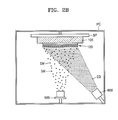
- FIGS. 2A through 2D illustrate diagrams of stages in a method of manufacturing the display apparatus 100 , according to an embodiment.
- FIGS. 2A through 2D sequentially show the method of manufacturing the display apparatus 100 of FIG. 1 .
- the method of manufacturing a display apparatus may be applied to various types of display apparatuses besides the display apparatus 100 of FIG. 1 .
- the display device 120 may be formed on the substrate 101 . As described in the embodiment of FIG. 1 , the display device 120 may have a variety of shapes. When the display device 120 includes an organic light-emitting device, the display device 120 may include the first electrode 121 , the second electrode 122 , and the intermediate layer 123 .
- the display apparatus 100 may further include a TFT (not shown) and a capacitor (not shown) that are electrically connected to the display device 120 .
- the thin-film encapsulation layer 150 may be formed on the display device 120 .
- a process of manufacturing the thin-film encapsulation layer 150 may be performed by using a source material-providing unit 500 and an energy beam irradiating unit 600 .
- the process of manufacturing the thin-film encapsulation layer 150 may be performed in a process chamber (PC). As shown in FIG. 2A , a structure in which the display device 120 is formed on the substrate 101 may be arranged in the PC. In this regard, a process of forming the thin-film encapsulation layer 150 while the substrate 101 is arranged on a supporter SP may be performed. In an implementation, a fixing member (not shown) may be further included to stably fix the substrate 101 on the supporter SP.
- a vacuous, vacuum, or low-pressure atmosphere may be maintained in the PC in order to effectively perform processes to be described below or to help improve features of the thin-film encapsulation layer 150 .
- a pressure control member e.g., a pump (not shown), may be connected to the PC.
- the source material-providing unit 500 and the energy beam irradiating unit 600 may be arranged in the PC.
- the source material-providing unit 500 and the energy beam irradiating unit 600 may be arranged to face the display device 120 .
- the substrate 101 may be arranged on the supporter SP in the PC, and the source material-providing unit 500 and the energy beam irradiating unit 600 may be arranged at a bottom, e.g., opposite end, of the PC.
- the source material-providing unit 500 may provide one or more source materials SM towards the display device 120 .
- Types of the source materials SM may vary, and the source materials SM include diverse suitable materials for forming the thin-film encapsulation layer 150 .
- the source materials SM may include at least one inorganic layer including LVT inorganic materials.
- the LVT inorganic materials may include a single compound or a combination of two or more compounds.
- the LVT inorganic materials may include tin oxide (e.g., SnO, SnO 2 , or the like).
- tin oxide e.g., SnO, SnO 2 , or the like.
- the content of SnO may be from about 20 weight % to about 100 weight %.
- the LVT inorganic materials may further include, e.g., at least one of phosphorus oxide (e.g., P 2 O 5 ), boron phosphate (BPO 4 ), tin fluoride (e.g., SnF 2 ), niobium oxide (e.g., NbO), tungsten oxide (e.g., WO 3 ), in addition to the tin oxide.
- phosphorus oxide e.g., P 2 O 5
- BPO 4 boron phosphate
- tin fluoride e.g., SnF 2
- niobium oxide e.g., NbO
- tungsten oxide e.g., WO 3
- the LVT inorganic materials may include:
- the LVT inorganic materials may have the following compositions, but the compositions are not limited thereto:
- the LVT inorganic materials may include SnO (42.5 wt %), SnF 2 (40 wt %), P 2 O 5 (15 wt %), and WO 3 (2.5 wt %).
- the LVT inorganic materials may include Al, C, ZnO, B 2 O 3 or BiO in addition to the tin oxide.
- a process of providing the source materials SM may include a spraying method or a sputtering method.
- the process of providing the source materials SM may be performed by co-deposition.
- the energy beam irradiating unit 600 may irradiate energy beams EB towards the substrate 101 , e.g., towards the display device 120 .
- the energy beam irradiating unit 600 may irradiate the energy beams EB during a process of providing the source materials SM to the display device 120 from the source material-providing unit 500 .
- the energy beam irradiating unit 600 may irradiate the energy beams EB that are in different forms, e.g., and may include at least one selected from the group of ion beams, electron beams, laser beams, and neutron beams.
- the energy beams EB may be energy beams EB formed using ionized inert gases. For example, when the energy beams EB use the ion beams, the energy beams EB may use the ionized inert gases.
- the energy beams EB irradiated by the energy beam irradiating unit 600 may increase a speed of providing the source materials SM.
- the thin-film encapsulation layer 150 may be quickly formed by using the provided source materials SM.
- the source materials SM may be uniformly and smoothly scattered or distributed on the display device 120 so that the thin-film encapsulation layer 150 may be formed even and dense.
- a process of effectively scattering the source materials SM may easily remove foreign materials that already exist on the display device 120 and/or may solve or correct for defects that may be generated on the display device 120 due to the source materials SM.
- the energy beam irradiating unit 600 may irradiate the energy beams EB once at or during at least one point of time that overlaps a process time when the source materials SM are provided from the source material-providing unit 500 to the display device 120 .
- the energy beam irradiating unit 600 may irradiate the energy beams EB at points of time that overlap the process time when the source materials SM are provided from the source material-providing unit 500 to the display device 120 .
- the energy beam irradiating unit 600 may periodically irradiate the energy beams EB at some points of time.
- the energy beam irradiating unit 600 may irregularly irradiate the energy beams EB at some points of time.
- the energy beam irradiating unit 600 and the source material-providing unit 500 may be arranged in various forms. In an implementation, as shown in FIG. 2B , the energy beam irradiating unit 600 and the source material-providing unit 500 may be obliquely arranged. For example, a direction in which the source materials SM are provided from the source material-providing unit 500 to the display device 120 and a direction in which the energy beam irradiating unit 600 irradiates the energy beams EB to the display device 120 may not be parallel, but rather may form a certain, e.g., oblique, angle.
- the direction in which the source materials SM are provided from the source material-providing unit 500 to the display device 120 may be perpendicular to the substrate 101
- the direction in which the energy beam irradiating unit 600 irradiates the energy beams EB to the display device 120 may be acute or obtuse relative to the substrate 101 and/or to the source material-providing unit 500 .
- a space within the PC may be efficiently used, and arranging the source material-providing unit 500 and the energy beam irradiating unit 600 may be easy.
- an influence of the energy beams EB of the energy beam irradiating unit 600 , which are not materials for forming the thin-film encapsulation layer 150 , e.g., that do not directly form the thin-film encapsulation layer 150 , on the display device 120 may be minimized.
- the energy beam irradiating unit 600 may include or provide at least one selected from the group of ion beams, electron beams, laser beams, and neutron beams.
- the energy beam irradiating unit 600 may use or provide both ion beams and electron beams as the energy beams EB. For example, positive charges or negative charges that may remain in the display device 120 may be neutralized by using the ion beams and the electron beams as the energy beams EB. Thus, the energy beam irradiating unit 600 may irradiate the electron beams right or immediately after irradiating the ion beams, or may irradiate the ion beams right or immediately after irradiating the electron beams. In an implementation, the ion beams and the electron beams may be alternately irradiated several times.
- the energy beam irradiating unit 600 may include irradiation members (not shown) to use or provide both ion beams and electron beams as the energy beams EB.
- One irradiation member may irradiate ion beams and another irradiation member may irradiate electron beams.
- the thin-film encapsulation layer 150 may be formed on the display device 120 , as shown in FIG. 2C . Then, as shown in FIG. 2D , the display apparatus 100 may be completely manufactured.
- the thin-film encapsulation layer 150 may be formed first and then a healing process may be further performed at a higher temperature than the viscosity transition temperature of the LVT inorganic materials but less than the denaturation temperature of the intermediate layer 123 of the display device 120 . Any defects that may exist in the thin-film encapsulation layer 150 may be corrected by performing the healing process.
- the energy beams EB may help increase the speed of providing the source materials SM during the process of providing the source materials SM as described above. Through the process, the source materials SM may be effectively scattered or distributed on the display device 120 . Thus, a speed of forming the thin-film encapsulation layer 150 may be advantageously increased. In addition, when the thin-film encapsulation layer 150 is formed, any defects that may be caused by the scattered source materials SM may be easily corrected.
- the defects may include impurities that are inevitably generated before or while the thin-film encapsulation layer 150 is formed, e.g., fine particles from the outside (e.g., dusts, specks, etc. from an external environment), residues that remain after the display device 120 is formed (e.g., fine particles, etc. including materials for forming the second electrode 122 which remain after the second electrode 122 is formed), or the like.
- the defects may be the result of particles including the LVT inorganic materials that are the source materials SM.
- the energy beams EB may help increase the speed of providing the source materials SM during the process of providing the source materials SM, and the aforementioned defects may be removed or corrected.
- the display apparatus 100 having the thin-film encapsulation layer 150 with improved durability which may easily help prevent moisture, impurities, or oxygen from penetrating into the display apparatus 100 , may be easily implemented.
- FIGS. 3A through 3E illustrate diagrams of stages in a method of manufacturing the display apparatus 100 , according to another embodiment.
- FIGS. 3A through 3E sequentially show the method of manufacturing the display apparatus 100 of FIG. 1 .
- the method of manufacturing a display apparatus may be applied to various types of display apparatuses besides the display apparatus 100 of FIG. 1 .
- a structure in which the display device 120 is formed on the substrate 101 may be prepared, and then the structure may be arranged in the PC.
- the display device 120 may have various forms.
- the display device 120 may include the first electrode 121 , the second electrode 122 , and the intermediate layer 123 .
- a process of forming the thin-film encapsulation layer 150 may be performed while the substrate 101 is arranged on the supporter SP.
- the source material-providing unit 500 and the energy beam irradiating unit 600 may be arranged in the PC.
- the source material-providing unit 500 and the energy beam irradiating unit 600 may be arranged to face the display device 120 .
- the source material-providing unit 500 may provide one or more source materials SM to the display device 120 .
- Types of the source materials SM may vary, and the source materials SM may include diverse suitable materials for forming the thin-film encapsulation layer 150 .
- the source materials SM may include at least one inorganic layer including LVT inorganic materials.
- a method of providing the source materials SM may be the same as various examples described in the previous embodiment.
- a preliminary thin-film encapsulation layer 150 ′ may be formed, as shown in FIG. 3B .
- one or more energy beams EB may be irradiated on the preliminary thin-film encapsulation layer 150 ′ by the energy beam irradiating unit 600 .
- the energy beams EB may be irradiated in a direction toward the substrate 101 , e.g., a direction toward the display device 120 .
- the energy beam irradiating unit 600 may irradiate the energy beams EB after the source materials SM have been provided in a direction toward the display device 120 .
- the energy beam irradiating unit 600 may irradiate energy beams EB that are in different forms.
- the irradiation of the energy beams EB that are in different forms is already described above, and thus, detailed descriptions thereof may not be repeated.
- the thin-film encapsulation layer 150 may be formed on the display device 120 , as shown in FIG. 3D .
- the display apparatus 100 may be completely manufactured as shown in FIG. 3E .
- the thin-film encapsulation layer 150 (e.g., the preliminary thin-film encapsulation layer 150 ′) may be formed first, and then a healing process may be further performed at a higher temperature than the viscosity transition temperature of the LVT inorganic materials but less than the denaturation temperature of the intermediate layer 123 of the display device 120 (e.g., to form the thin-film encapsulation layer 150 ). Any defects that may exist in the thin-film encapsulation layer 150 (e.g., the preliminary thin-film encapsulation layer 150 ′) may be corrected by performing the healing process.
- the process of providing the source materials SM may be performed to form the preliminary thin-film encapsulation layer 150 ′. Then, the energy beams EB may be irradiated on the preliminary thin-film encapsulation layer 150 ′.
- the source materials SM for forming the preliminary thin-film encapsulation layer 150 ′ through the above process may be effectively scattered or distributed on the display device 120 . Accordingly, the speed of forming the thin-film encapsulation layer 150 may be increased.
- defects that may be caused by the source materials SM that are scattered may be easily corrected.
- the display apparatus 100 having the thin-film encapsulation layer 150 with improved durability which may help prevent moisture, impurities, or oxygen from penetrating into the display apparatus 100 , may be easily implemented.
- FIG. 4 illustrates a diagram of a stage in a method of manufacturing the display apparatus 100 , according to another embodiment.
- FIG. 4 shows a stage in the method of manufacturing the display apparatus 100 of FIG. 1 .
- the method of the present embodiment may be applied to various display apparatuses.
- a structure in which the display device 120 is formed on the substrate 101 may be prepared, and the structure is arranged in the PC.
- the display device 120 may have various forms.
- the display device 120 may include the first electrode 121 , the second electrode 122 , and the intermediate layer 123 .
- a process of forming the thin-film encapsulation layer 150 may be performed while the substrate 101 is arranged on a supporter SP′.
- a cooling unit CU may be further arranged or provided to cool the substrate 101 .
- the cooling unit CU may be arranged to face the substrate 101 , e.g., the cooling unit CU may be connected to the supporter SP′.
- the supporter SP′ and the cooling unit CU may be integrated.
- the cooling unit CU may be provided to help prevent the substrate 101 from overheating during the process of forming the thin-film encapsulation layer 150 . Through the process, the denaturation of the display device 120 , e.g., the intermediate layer 123 , may be effectively prevented.
- FIG. 5 illustrates a diagram of a stage in a method of manufacturing the display apparatus 100 , according to another embodiment.
- FIG. 5 shows the method of manufacturing the display apparatus 100 of FIG. 1 .
- the method of manufacturing a display apparatus may be applied to various types of display apparatuses besides the display apparatus 100 of FIG. 1 .
- a structure in which the display device 120 is formed on the substrate 101 may be prepared, and the structure is arranged in the PC.
- the display device 120 may have various forms.
- the display device 120 may include the first electrode 121 , the second electrode 122 , and the intermediate layer 123 .
- a process of forming the thin-film encapsulation layer 150 may be performed while the substrate 101 is arranged on the supporter SP′. While the thin-film encapsulation layer 150 is being formed on the substrate 101 , a peripheral gas providing unit (PG) may make peripheral gases flow around the substrate 101 .
- PG peripheral gas providing unit
- the peripheral gases may include, e.g., oxygen, nitrogen, or an oxynitride gas.
- the peripheral gas may include oxygen gas (O 2 ), nitrogen gas (N 2 ), and/or an oxynitride-containing gas.
- the peripheral gases may be provided during the process of forming the thin-film encapsulation layer 150 , e.g., while the thin-film encapsulation layer 150 is formed by providing the source materials SM from the source material-providing unit 500 to the display device 120 .
- the reactivity of the LVT inorganic materials included in the source materials SM may be improved.
- an oxidation reaction or nitrification reaction may be improved. Through the reaction, the speed of forming the thin-film encapsulation layer 150 may be increased, and an encapsulation feature thereof may be improved.
- the remaining processes may be the same as or may be slightly modified from the embodiments described with reference to FIGS. 2A through 2D or FIGS. 3A through 3E .
- the cooling unit CU of FIG. 4 may also be applied to the embodiment of FIG. 5 .
- a display apparatus with improved encapsulation features may be manufactured by a method of manufacturing a display apparatus.
- a display device included in the display apparatus may be vulnerable to moisture, impurities, or heat from the outside, and the moisture, impurities, or heat may damage the display device or cause the malfunction of the display device.
- the embodiments provide an encapsulation structure for encapsulating the display device.
Landscapes
- Chemical & Material Sciences (AREA)
- Mechanical Engineering (AREA)
- Chemical Kinetics & Catalysis (AREA)
- Engineering & Computer Science (AREA)
- Materials Engineering (AREA)
- Metallurgy (AREA)
- Organic Chemistry (AREA)
- Optics & Photonics (AREA)
- Physics & Mathematics (AREA)
- Electroluminescent Light Sources (AREA)
- Health & Medical Sciences (AREA)
- Toxicology (AREA)
- General Chemical & Material Sciences (AREA)
Abstract
Description
Claims (19)
Applications Claiming Priority (2)
| Application Number | Priority Date | Filing Date | Title |
|---|---|---|---|
| KR10-2014-0072301 | 2014-06-13 | ||
| KR1020140072301A KR20150143966A (en) | 2014-06-13 | 2014-06-13 | Method for manufacturing display apparatus |
Publications (2)
| Publication Number | Publication Date |
|---|---|
| US20150364719A1 US20150364719A1 (en) | 2015-12-17 |
| US9614182B2 true US9614182B2 (en) | 2017-04-04 |
Family
ID=54836918
Family Applications (1)
| Application Number | Title | Priority Date | Filing Date |
|---|---|---|---|
| US14/531,302 Expired - Fee Related US9614182B2 (en) | 2014-06-13 | 2014-11-03 | Method of manufacturing display apparatus that includes using an energy beam to form an encapsulation layer |
Country Status (2)
| Country | Link |
|---|---|
| US (1) | US9614182B2 (en) |
| KR (1) | KR20150143966A (en) |
Citations (5)
| Publication number | Priority date | Publication date | Assignee | Title |
|---|---|---|---|---|
| KR20080045217A (en) | 2005-08-18 | 2008-05-22 | 코닝 인코포레이티드 | Method for suppressing oxygen and moisture decomposition for device and device accordingly |
| US20080290798A1 (en) | 2007-05-22 | 2008-11-27 | Mark Alejandro Quesada | LLT barrier layer for top emission display device, method and apparatus |
| KR20100050470A (en) | 2007-06-21 | 2010-05-13 | 코닝 인코포레이티드 | Sealing technique and hermetically sealed device |
| US8304990B2 (en) | 2005-08-18 | 2012-11-06 | Corning Incorporated | Hermetically sealing a device without a heat treating step and the resulting hermetically sealed device |
| US20130230665A1 (en) * | 2012-03-05 | 2013-09-05 | Jin-woo Park | Method of preparing organic light-emitting device |
-
2014
- 2014-06-13 KR KR1020140072301A patent/KR20150143966A/en not_active Ceased
- 2014-11-03 US US14/531,302 patent/US9614182B2/en not_active Expired - Fee Related
Patent Citations (7)
| Publication number | Priority date | Publication date | Assignee | Title |
|---|---|---|---|---|
| KR20080045217A (en) | 2005-08-18 | 2008-05-22 | 코닝 인코포레이티드 | Method for suppressing oxygen and moisture decomposition for device and device accordingly |
| US8304990B2 (en) | 2005-08-18 | 2012-11-06 | Corning Incorporated | Hermetically sealing a device without a heat treating step and the resulting hermetically sealed device |
| US8435604B2 (en) | 2005-08-18 | 2013-05-07 | Corning Incorporated | Sealing technique for decreasing the time it takes to hermetically seal a device and the resulting hermetically sealed device |
| US20080290798A1 (en) | 2007-05-22 | 2008-11-27 | Mark Alejandro Quesada | LLT barrier layer for top emission display device, method and apparatus |
| KR20100029774A (en) | 2007-05-22 | 2010-03-17 | 코닝 인코포레이티드 | Llt barrier layer for top emission display device, method and apparatus |
| KR20100050470A (en) | 2007-06-21 | 2010-05-13 | 코닝 인코포레이티드 | Sealing technique and hermetically sealed device |
| US20130230665A1 (en) * | 2012-03-05 | 2013-09-05 | Jin-woo Park | Method of preparing organic light-emitting device |
Also Published As
| Publication number | Publication date |
|---|---|
| US20150364719A1 (en) | 2015-12-17 |
| KR20150143966A (en) | 2015-12-24 |
Similar Documents
| Publication | Publication Date | Title |
|---|---|---|
| US9881985B2 (en) | OLED device, AMOLED display device and method for manufacturing same | |
| TWI679791B (en) | Light emitting element, display device and lighting device | |
| WO2012114403A1 (en) | Organic electroluminescence display panel and organic electroluminescence display device | |
| EP2793282B1 (en) | Organic light-emitting display device and method of preparing the same | |
| US9076984B2 (en) | Mother panel for display panel and method of manufacturing display panel using the mother panel | |
| KR20140000426A (en) | Substrate for oled and method for fabricating thereof | |
| CN102569678A (en) | Composite thin film packaging method of top emission OLED (Organic Light Emitting Diode) | |
| US20150267290A1 (en) | Deposition source, deposition apparatus, and method of manufacturing organic light-emitting display apparatus | |
| KR102072806B1 (en) | Organic light emitting display device and method of manufacturing the same | |
| KR102314466B1 (en) | Apparatus for manufacturing display apparatus and method of manufacturing display apparatus | |
| US20190393449A1 (en) | Organic light emitting display device | |
| US9614182B2 (en) | Method of manufacturing display apparatus that includes using an energy beam to form an encapsulation layer | |
| JP6322380B2 (en) | Display device | |
| US9299957B2 (en) | Method of manufacturing organic light emitting display apparatus by performing plasma surface process using target sputtering apparatus | |
| US20090051280A1 (en) | Light-emitting device, method for manufacturing light-emitting device, and substrate processing apparatus | |
| KR20150019886A (en) | Method for manufacturing organic light-emitting display apparatus | |
| CN104701343A (en) | Organic EL display device and method for manufacturing same | |
| KR102093392B1 (en) | Organic light-emitting display apparatus and method for manufacturing the same | |
| US9634283B2 (en) | Low temperature viscosity transition composition, display apparatus including the same, and method of manufacturing the same | |
| KR20140059376A (en) | Apparatus for manufacturing organic layer and method for manufacturing organic light emitting display | |
| KR102169595B1 (en) | Deposition apparatus and manufacturing method of organic light emitting display using the same | |
| JP7705734B2 (en) | Organic light-emitting element, film formation method, and film formation apparatus | |
| JP4925903B2 (en) | Organic EL device, organic EL device manufacturing method | |
| KR102107997B1 (en) | Method for Processing Surface of Transparent Film, Organic Light Emitting Device Manufactured Using That Method, and Method for Manufacturing That Organic Light Emitting Device | |
| CN109411637A (en) | A kind of processing method of top emitting Organic Light Emitting Diode metal anode |
Legal Events
| Date | Code | Title | Description |
|---|---|---|---|
| AS | Assignment |
Owner name: SAMSUNG DISPLAY CO., LTD., KOREA, REPUBLIC OF Free format text: ASSIGNMENT OF ASSIGNORS INTEREST;ASSIGNOR:CHOI, JAI-HYUK;REEL/FRAME:034091/0466 Effective date: 20141028 |
|
| FEPP | Fee payment procedure |
Free format text: PAYOR NUMBER ASSIGNED (ORIGINAL EVENT CODE: ASPN); ENTITY STATUS OF PATENT OWNER: LARGE ENTITY |
|
| STCF | Information on status: patent grant |
Free format text: PATENTED CASE |
|
| FEPP | Fee payment procedure |
Free format text: MAINTENANCE FEE REMINDER MAILED (ORIGINAL EVENT CODE: REM.); ENTITY STATUS OF PATENT OWNER: LARGE ENTITY |
|
| LAPS | Lapse for failure to pay maintenance fees |
Free format text: PATENT EXPIRED FOR FAILURE TO PAY MAINTENANCE FEES (ORIGINAL EVENT CODE: EXP.); ENTITY STATUS OF PATENT OWNER: LARGE ENTITY |
|
| STCH | Information on status: patent discontinuation |
Free format text: PATENT EXPIRED DUE TO NONPAYMENT OF MAINTENANCE FEES UNDER 37 CFR 1.362 |
|
| FP | Lapsed due to failure to pay maintenance fee |
Effective date: 20210404 |