US9614064B2 - Semiconductor device and integrated circuit - Google Patents
Semiconductor device and integrated circuit Download PDFInfo
- Publication number
- US9614064B2 US9614064B2 US14/673,072 US201514673072A US9614064B2 US 9614064 B2 US9614064 B2 US 9614064B2 US 201514673072 A US201514673072 A US 201514673072A US 9614064 B2 US9614064 B2 US 9614064B2
- Authority
- US
- United States
- Prior art keywords
- body region
- region
- main surface
- width
- semiconductor device
- Prior art date
- Legal status (The legal status is an assumption and is not a legal conclusion. Google has not performed a legal analysis and makes no representation as to the accuracy of the status listed.)
- Expired - Fee Related
Links
Images


Classifications
-
- H—ELECTRICITY
- H10—SEMICONDUCTOR DEVICES; ELECTRIC SOLID-STATE DEVICES NOT OTHERWISE PROVIDED FOR
- H10D—INORGANIC ELECTRIC SEMICONDUCTOR DEVICES
- H10D10/00—Bipolar junction transistors [BJT]
- H10D10/60—Lateral BJTs
-
- H01L29/735—
-
- H01L29/0657—
-
- H01L29/407—
-
- H01L29/41708—
-
- H01L29/41766—
-
- H01L29/42304—
-
- H01L29/4236—
-
- H01L29/7816—
-
- H01L29/7825—
-
- H01L29/808—
-
- H—ELECTRICITY
- H10—SEMICONDUCTOR DEVICES; ELECTRIC SOLID-STATE DEVICES NOT OTHERWISE PROVIDED FOR
- H10D—INORGANIC ELECTRIC SEMICONDUCTOR DEVICES
- H10D30/00—Field-effect transistors [FET]
- H10D30/60—Insulated-gate field-effect transistors [IGFET]
- H10D30/62—Fin field-effect transistors [FinFET]
-
- H—ELECTRICITY
- H10—SEMICONDUCTOR DEVICES; ELECTRIC SOLID-STATE DEVICES NOT OTHERWISE PROVIDED FOR
- H10D—INORGANIC ELECTRIC SEMICONDUCTOR DEVICES
- H10D30/00—Field-effect transistors [FET]
- H10D30/60—Insulated-gate field-effect transistors [IGFET]
- H10D30/64—Double-diffused metal-oxide semiconductor [DMOS] FETs
- H10D30/65—Lateral DMOS [LDMOS] FETs
- H10D30/658—Lateral DMOS [LDMOS] FETs having trench gate electrodes
-
- H—ELECTRICITY
- H10—SEMICONDUCTOR DEVICES; ELECTRIC SOLID-STATE DEVICES NOT OTHERWISE PROVIDED FOR
- H10D—INORGANIC ELECTRIC SEMICONDUCTOR DEVICES
- H10D30/00—Field-effect transistors [FET]
- H10D30/80—FETs having rectifying junction gate electrodes
- H10D30/83—FETs having PN junction gate electrodes
-
- H—ELECTRICITY
- H10—SEMICONDUCTOR DEVICES; ELECTRIC SOLID-STATE DEVICES NOT OTHERWISE PROVIDED FOR
- H10D—INORGANIC ELECTRIC SEMICONDUCTOR DEVICES
- H10D62/00—Semiconductor bodies, or regions thereof, of devices having potential barriers
- H10D62/10—Shapes, relative sizes or dispositions of the regions of the semiconductor bodies; Shapes of the semiconductor bodies
- H10D62/117—Shapes of semiconductor bodies
-
- H—ELECTRICITY
- H10—SEMICONDUCTOR DEVICES; ELECTRIC SOLID-STATE DEVICES NOT OTHERWISE PROVIDED FOR
- H10D—INORGANIC ELECTRIC SEMICONDUCTOR DEVICES
- H10D62/00—Semiconductor bodies, or regions thereof, of devices having potential barriers
- H10D62/10—Shapes, relative sizes or dispositions of the regions of the semiconductor bodies; Shapes of the semiconductor bodies
- H10D62/17—Semiconductor regions connected to electrodes not carrying current to be rectified, amplified or switched, e.g. channel regions
- H10D62/213—Channel regions of field-effect devices
- H10D62/221—Channel regions of field-effect devices of FETs
- H10D62/235—Channel regions of field-effect devices of FETs of IGFETs
-
- H—ELECTRICITY
- H10—SEMICONDUCTOR DEVICES; ELECTRIC SOLID-STATE DEVICES NOT OTHERWISE PROVIDED FOR
- H10D—INORGANIC ELECTRIC SEMICONDUCTOR DEVICES
- H10D64/00—Electrodes of devices having potential barriers
- H10D64/111—Field plates
- H10D64/117—Recessed field plates, e.g. trench field plates or buried field plates
-
- H—ELECTRICITY
- H10—SEMICONDUCTOR DEVICES; ELECTRIC SOLID-STATE DEVICES NOT OTHERWISE PROVIDED FOR
- H10D—INORGANIC ELECTRIC SEMICONDUCTOR DEVICES
- H10D64/00—Electrodes of devices having potential barriers
- H10D64/20—Electrodes characterised by their shapes, relative sizes or dispositions
- H10D64/23—Electrodes carrying the current to be rectified, amplified, oscillated or switched, e.g. sources, drains, anodes or cathodes
- H10D64/231—Emitter or collector electrodes for bipolar transistors
-
- H—ELECTRICITY
- H10—SEMICONDUCTOR DEVICES; ELECTRIC SOLID-STATE DEVICES NOT OTHERWISE PROVIDED FOR
- H10D—INORGANIC ELECTRIC SEMICONDUCTOR DEVICES
- H10D64/00—Electrodes of devices having potential barriers
- H10D64/20—Electrodes characterised by their shapes, relative sizes or dispositions
- H10D64/23—Electrodes carrying the current to be rectified, amplified, oscillated or switched, e.g. sources, drains, anodes or cathodes
- H10D64/251—Source or drain electrodes for field-effect devices
- H10D64/256—Source or drain electrodes for field-effect devices for lateral devices wherein the source or drain electrodes are recessed in semiconductor bodies
-
- H—ELECTRICITY
- H10—SEMICONDUCTOR DEVICES; ELECTRIC SOLID-STATE DEVICES NOT OTHERWISE PROVIDED FOR
- H10D—INORGANIC ELECTRIC SEMICONDUCTOR DEVICES
- H10D64/00—Electrodes of devices having potential barriers
- H10D64/20—Electrodes characterised by their shapes, relative sizes or dispositions
- H10D64/27—Electrodes not carrying the current to be rectified, amplified, oscillated or switched, e.g. gates
- H10D64/281—Base electrodes for bipolar transistors
-
- H—ELECTRICITY
- H10—SEMICONDUCTOR DEVICES; ELECTRIC SOLID-STATE DEVICES NOT OTHERWISE PROVIDED FOR
- H10D—INORGANIC ELECTRIC SEMICONDUCTOR DEVICES
- H10D64/00—Electrodes of devices having potential barriers
- H10D64/20—Electrodes characterised by their shapes, relative sizes or dispositions
- H10D64/27—Electrodes not carrying the current to be rectified, amplified, oscillated or switched, e.g. gates
- H10D64/311—Gate electrodes for field-effect devices
- H10D64/411—Gate electrodes for field-effect devices for FETs
- H10D64/511—Gate electrodes for field-effect devices for FETs for IGFETs
- H10D64/512—Disposition of the gate electrodes, e.g. buried gates
- H10D64/513—Disposition of the gate electrodes, e.g. buried gates within recesses in the substrate, e.g. trench gates, groove gates or buried gates
-
- H01L29/1066—
-
- H—ELECTRICITY
- H10—SEMICONDUCTOR DEVICES; ELECTRIC SOLID-STATE DEVICES NOT OTHERWISE PROVIDED FOR
- H10D—INORGANIC ELECTRIC SEMICONDUCTOR DEVICES
- H10D62/00—Semiconductor bodies, or regions thereof, of devices having potential barriers
- H10D62/10—Shapes, relative sizes or dispositions of the regions of the semiconductor bodies; Shapes of the semiconductor bodies
- H10D62/17—Semiconductor regions connected to electrodes not carrying current to be rectified, amplified or switched, e.g. channel regions
- H10D62/343—Gate regions of field-effect devices having PN junction gates
Definitions
- MOS metal oxide semiconductor
- Lateral power devices in which current flow mainly takes place parallel to a main surface of a semiconductor substrate, are useful for semiconductor devices in which further components, such as switches, bridges and control circuits are integrated.
- safe operating area This applies on one side to the linear operation region at higher gate voltages as well as to the resistance to avalanche breakdown at a gate-source voltage of 0 V.
- the transistor comprises a source region, a drain region, a body region, and a gate electrode structure adjacent to the body region.
- the source region and the drain region are disposed along a first direction which is parallel to the main surface.
- the body region is disposed between the source region and the drain region.
- the body region comprises an upper body region at the main surface and a lower body region remote from the main surface, a first width of the lower body region being smaller than a second width of the upper body region, the first width and the second width being measured in a direction perpendicular to the first direction.
- a semiconductor device comprising a transistor in a semiconductor substrate including a main surface
- the transistor comprises a source region, a drain region, a body region including a channel region, a gate electrode structure adjacent to the body region, and a body contact portion in contact with the body region.
- the source region and the drain region are disposed along a first direction, the first direction being parallel to the main surface.
- the body region is disposed between the source region and the drain region.
- the body region has a shape of a fin extending along the first direction, the fin having a top side at the main surface and two sidewalls.
- the body contact portion contacts the top side of the fin.
- a semiconductor device comprising a transistor in a semiconductor substrate including a main surface
- the transistor comprises a source region, a drain region, a body region disposed between the source region and the drain region, a gate electrode structure adjacent to the body region, and a body contact portion in contact with a top surface of the body region.
- the body contact portion is electrically coupled to a source terminal.
- the top surface is disposed on a side of the main surface of the semiconductor substrate.
- the source region and the drain region are disposed along a first direction, the first direction being parallel to the main surface.
- FIG. 1A shows a cross-sectional view of a semiconductor device according to an embodiment in a plane parallel to a main surface of a semiconductor substrate;
- FIG. 1B shows a further cross-sectional view of the semiconductor device shown in FIG. 1A ;
- FIG. 1C shows a cross-sectional view of a semiconductor device according to a further embodiment in a plane parallel to a main surface of a semiconductor substrate;
- FIG. 1D shows a further cross-sectional view of the semiconductor device shown in FIG. 1C ;
- FIG. 2A shows a cross-sectional view of a semiconductor device according to a further embodiment in a plane parallel to a main surface of a semiconductor substrate;
- FIG. 2B shows a first cross-sectional view of the semiconductor device shown in FIG. 2A ;
- FIG. 2C shows a cross-sectional view of the semiconductor device shown in FIG. 2A in a direction perpendicular to the direction of the cross-sectional view of FIG. 2B ;
- FIG. 2D shows a cross-sectional view of a semiconductor device according to the embodiment of FIG. 2A in another plane parallel to a main surface of a semiconductor substrate;
- FIG. 2E shows a cross-sectional view of a semiconductor device corresponding to the cross-sectional view of FIG. 2D including a modification
- FIG. 2F shows a cross-sectional view of the semiconductor device corresponding to the cross-sectional view of FIG. 2C taken at a different position
- FIG. 2G shows a cross-sectional view of a further portion of the semiconductor device shown in FIG. 2A in a direction perpendicular to the direction of the cross-sectional view of FIG. 2B ;
- FIG. 3A shows a cross-sectional view of a semiconductor device according to a further embodiment
- FIG. 3B shows a cross-sectional view of the semiconductor device of FIG. 3A in a direction perpendicular to the direction of the cross-sectional view of FIG. 3A ;
- FIGS. 4A and 4B illustrate equivalent circuit diagrams of converters according to embodiments.
- wafer may include any semiconductor-based structure that has a semiconductor surface.
- Wafer and structure are to be understood to include silicon, silicon-on-insulator (SOI), silicon-on sapphire (SOS), doped and undoped semiconductors, epitaxial layers of silicon supported by a base semiconductor foundation, and other semiconductor structures.
- SOI silicon-on-insulator
- SOS silicon-on sapphire
- the semiconductor need not be silicon-based.
- the semiconductor could as well be silicon-germanium, germanium, or gallium arsenide.
- silicon carbide (SiC) or gallium nitride (GaN) may form the semiconductor substrate material.
- lateral and “horizontal” as used in this specification intends to describe an orientation parallel to a first surface of a semiconductor substrate or semiconductor body. This can be for instance the surface of a wafer or a die.
- vertical as used in this specification intends to describe an orientation which is arranged perpendicular to the first surface of the semiconductor substrate or semiconductor body.
- n ⁇ means a doping concentration which is lower than the doping concentration of an “n”-doping region while an “n + ”-doping region has a higher doping concentration than an “n”-doping region.
- Doping regions of the same relative doping concentration do not necessarily have the same absolute doping concentration.
- two different “n”-doping regions may have the same or different absolute doping concentrations.
- the doped portions are designated as being “p” or “n”-doped. As is clearly to be understood, this designation is by no means intended to be limiting.
- the doping type can be arbitrary as long as the described functionality is achieved. Further, in all embodiments, the doping types can be reversed.
- Coupled and/or “electrically coupled” are not meant to mean that the elements must be directly coupled together—intervening elements may be provided between the “coupled” or “electrically coupled” elements.
- electrically connected intends to describe a low-ohmic electric connection between the elements electrically connected together.
- MOSFETs may be n-channel or p-channel MOSFETs.
- MOSFETs may be n-channel or p-channel MOSFETs.
- the source and the drain region are doped with n-type dopants, and the current direction is from the drain region to the source region.
- the source and the drain region are doped with p-type dopants, and the current direction is from the source region to the drain region.
- the doping types may be reversed. If a specific current path is described using directional language, this description is to be merely understood to indicate the path and not the polarity of the current flow, i.e. whether the transistor is a p-channel or an n-channel transistor.
- the Figures may include polarity-sensitive components, e.g. diodes. As is to be clearly understood, the specific arrangement of these polarity-sensitive components is given as an example and may be inverted in order to achieve the described functionality, depending whether the first conductivity type means n-type or p-type.
- Embodiments are described while specifically referring to so-called normally-off transistors, i.e. transistors which are in an off-state when no gate voltage or a gate voltage of 0V is applied.
- normally-off transistors i.e. transistors which are in an off-state when no gate voltage or a gate voltage of 0V is applied.
- normally-on transistors i.e. transistors which are in a conducting state when no gate voltage or a gate voltage of 0V is applied.
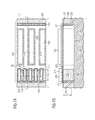
- FIG. 1A shows a cross-sectional view of a semiconductor device 1 or an integrated circuit which is taken in a plane parallel to main surface of a semiconductor substrate.
- the semiconductor device 1 comprises a transistor 200 in a semiconductor substrate including a main surface.
- the transistor 200 comprises a source region 201 , a drain region 205 and a body region 220 .
- the transistor further comprises a gate electrode structure 209 that is adjacent to the body region 220 .
- the gate electrode structure 209 may comprise a gate dielectric 211 and a gate electrode 210 , the gate dielectric 211 being disposed between the gate electrode 210 and the body region 220 .
- the source region 201 and the drain region 205 are disposed along a first direction, the first direction being parallel to the main surface.
- the body region 220 is disposed between the source region 201 and the drain region 205 .
- FIG. 1B shows a cross-sectional view between II and II′ as is also indicated in FIG. 1A , showing the semiconductor substrate 100 and the main surface 110 .
- the body region 220 comprises an upper body region 212 at the main surface 110 and a lower body region 213 remote from the main surface 110 .
- a first width of the lower body region 213 is smaller than a second width of the upper body region 212 .
- the first width and the second width are measured in a direction perpendicular to the first direction.
- the source region 201 may be electrically coupled to the source electrode 202 .
- the drain region 205 may be electrically coupled to the drain electrode 206 .
- the source electrode 202 and the drain electrode 206 may be disposed in respective contact trenches extending perpendicularly with respect to the first direction.
- FIGS. 1C and 1D illustrate elements of a semiconductor device according to further embodiments.
- a semiconductor device 1 comprises a transistor 200 in a semiconductor substrate 100 including a main surface 110 .
- the transistor 200 comprises a source region 201 , a drain region 205 , a body region 220 , the body region 220 being disposed between the source region 201 and the drain region 205 .
- the transistor further comprises a gate electrode structure 209 adjacent to the body region 220 .
- the gate electrode structure 209 may comprise a gate electrode 210 and a gate dielectric 211 disposed between the gate electrode 210 and the body region 220 .
- the transistor 200 further comprises a body contact portion 225 in contact with a top surface of the body region 220 , the body contact portion being electrically coupled to a source terminal 226 .
- the top surface of the body region is disposed on a side of the main surface 110 of the semiconductor substrate 100 .
- the source region and the drain region 201 , 205 are disposed along a first direction, the first direction being parallel to the main surface 110 .
- the body contact portion is electrically coupled to a source terminal 226 via a source connection wiring 227 .
- this electrically connection may be implemented in an alternative manner.
- FIGS. 1C and 1D show cross-sectional views of a semiconductor device according to still a further embodiment.
- the semiconductor device 1 shown in FIGS. 1C and 1D comprises a transistor 200 in a semiconductor substrate 100 including a main surface 110 .
- the transistor 200 comprises a source region 201 , a drain region 205 and a body region 220 .
- the body region 220 includes a channel region 213 .
- the transistor further comprises a gate electrode structure 209 .
- the gate electrode structure 209 may comprise a gate dielectric 211 and a gate electrode 210 , the gate dielectric 211 being disposed between the gate electrode 210 and the body region 220 .
- the semiconductor device further comprises a body contact portion 225 in contact with the body region 220 .
- the source region 201 and the drain region 205 are disposed along a first direction that is parallel to the main surface 110 .
- the body region 220 is disposed between the source region 201 and the drain region 205 .
- the body region 220 has a shape of a fin extending along the first direction.
- the fin has a top side 220 a at the main surface 110 and to sidewalls 220 b .
- the body contact portion 225 contacts the top side 220 a of the fin.
- the transistor 200 When a suitable voltage is applied to the gate electrode 210 , an inversion layer is formed at the boundary between the body region 220 and the gate electrode structure 209 . Accordingly, the transistor 200 is in a conducting state from the source region 201 to the drain region 205 .
- the conductivity of the channel that is defined in the body region 220 is controlled by the gate electrode forming a component of the gate electrode structure 209 . By controlling the conductivity of the channel formed in the body region 220 , the current flow from the source region 201 via the channel formed in the body region 220 to the drain region 205 may be controlled.
- the transistor When the transistor is switched off, no conductive channel is formed at the boundary between the body region 220 and the gate electrode structure 209 so that a sub-threshold current flows.
- the upper body region may be easily contacted and the upper body region may have a low resistance value.
- the lower body region may be fully depleted by applying suitable gate voltage to the gate electrodes 210 .
- the semiconductor device is optimized in view of the channel width which is determined by the first width and the width of the upper body region which enables low-ohmic contacts to the body region.
- the structure illustrated in FIGS. 1A to 1D enables body contact portions having a low resistivity. Thereby a low-ohmic contact of the body region to a source terminal is enabled and a parasitic bipolar transistor may be deteriorated or suppressed.
- FIG. 2A shows a cross-sectional view of a semiconductor device 1 or an integrated circuit according to a further embodiment.
- the cross-sectional view of FIG. 2A is taken between V and V′ as is also indicated in FIG. 2C , in other words, the cross-sectional view of FIG. 2A is taken close to the main surface of the semiconductor substrate.
- the semiconductor device 1 includes a transistor 200 .
- the transistor 200 shown in FIG. 2A comprises a source region 201 , a drain region 205 , a body region 220 , and a drift zone 260 .
- the source region 201 , the drain region 205 and the drift zone 260 may be doped with dopants of a first conductivity type, for example n-type dopants.
- the doping concentration of the source and the drain regions 201 , 205 may be higher than the doping concentration of the drift zone 260 .
- the body region 220 is arranged between the source region 201 and the drift zone 260 .
- the body region 220 is doped with dopants of a second conductivity type, for example with p-type dopants.
- the drift zone 260 may be arranged between the body region 220 and the drain region 205 .
- the source region 201 , the body region 220 , the drift zone 260 and the drain region 205 are disposed along a first direction parallel to a main surface 110 of the semiconductor substrate 100 .
- the source region 201 is connected to the source electrode 202 .
- the drain region 205 is connected to the drain electrode 206 .
- the semiconductor device 1 further comprises a gate electrode structure 209 .
- the gate electrode structure 209 may comprise a gate electrode 210 that may be insulated from the body region 220 by means of an insulating gate dielectric material 211 such as silicon oxide.
- the gate electrode structure 209 does not comprise a gate dielectric layer and the device may implement a JFET (“junction field effect transistor”), for example.
- the transistor may further comprise a field plate 250 which is arranged adjacent to the drift zone 260 .
- the field plate 250 is insulated from the drift zone 260 by means of an insulating field dielectric layer 251 such as silicon oxide.
- the transistor 200 is a lateral transistor. Accordingly, a current flow from the source region 201 to the drain region 205 is mainly accomplished in the first direction parallel to the main surface of the semiconductor substrate.
- the transistor When a suitable voltage is applied to the gate electrode 210 , an inversion layer is formed at the boundary between the body region 220 and the insulating gate dielectric material 211 . Accordingly, the transistor is in a conducting state from the source region 201 to the drain region 205 via the drift zone 260 .
- the conductivity of the channel that is formed in the body region 220 is controlled by the gate electrode. By controlling the conductivity of the channel formed in the channel region, the current flow from the source region 201 via the channel formed in the body region 220 and the drift zone 260 to the drain region 205 may be controlled.
- the transistor may be implemented as a normally-off transistor. According to a further embodiment, the transistor may be implemented as a normally-on transistor.
- the body region 220 may be doped with dopants of the first conductivity type, for example, with n-type dopants.
- An appropriate voltage may be applied to the field plate in an off-state.
- the field plate 250 may be electrically coupled to a source terminal, which is also electrically coupled to a source electrode 202 .
- the field plate 250 depletes charge carriers from the drift zone 260 so that the breakdown voltage characteristics of the transistor 200 are improved.
- the doping concentration of the drift zone 260 may be increased without deteriorating the breakdown voltage characteristics in comparison to a device without a field plate. Due to the higher doping concentration of the drift zone, the on-resistance RDS on is further decreased resulting in improved device characteristics.
- FIG. 2B illustrates a cross-sectional view of the semiconductor device 1 between I and I′ along the first direction, as is also indicated in FIG. 2A .
- the cross-sectional view of FIG. 2B is taken so as to intersect the body region 220 and the drift zone 260 .
- gate trenches 242 are disposed adjacent to the body region 220 in a plane before and behind the depicted plane of the drawing.
- field plate trenches 252 may be disposed adjacent to the drift zone 260 in a plane before and behind the depicted plane of the drawing.
- the gate trench 242 and the field plate trench 252 extend from the main surface 110 in a depth direction of the substrate 100 .
- the gate electrode is adjacent to at least two sides, e.g. opposing sides, of the body region 220 .
- the body region 220 has the shape of a first ridge.
- the drift zone 260 may have the shape of a second ridge.
- the source region 201 extends from the main surface 110 into a depth direction of the substrate 100 , i.e. perpendicularly with respect to the main surface 110 .
- the drain region 205 likewise extends from the main surface 110 in a depth direction of the substrate 100 .
- FIG. 2C illustrates a cross-sectional view of the semiconductor device which is taken between II and II′ as is also indicated in FIG. 2A .
- the direction between II and II′ is perpendicular to the first direction.
- the body region 220 has the shape of a ridge or a fin.
- the ridge may have a top side 220 a , and first and second sidewalls 220 b.
- the body region 220 comprises a lower body region 213 having a first width d 1 , and an upper body region 212 having a second width d 2 , the first and the second width being measured in the direction of i.e. perpendicularly to the first direction.
- conductive inversion layers are formed along the first and second sidewalls 220 b.
- the width d 1 of the lower body region 220 fulfills the following relationship: d 1 ⁇ 2*l d , wherein l d denotes a length of a depletion zone which is formed at the interface between the gate dielectric layer 211 and the body region 220 .
- the maximum width of the depletion zone may be determined as:
- k denotes the Boltzmann constant (1.38066 ⁇ 10 ⁇ 23 J/k)
- T denotes the temperature
- ln the denotes the natural logarithm
- N A denotes the impurity concentration of the semiconductor body
- n i denotes the intrinsic carrier concentration (1.45 ⁇ 10 10 cm ⁇ 3 for silicon at 27° C.)
- q denotes the elementary charge (1.6 ⁇ 10 ⁇ 19 C).
- the length of the depletion zone varies depending from the gate voltage. It is assumed that in a transistor the length of the depletion zone at a gate voltage corresponding to the threshold voltage corresponds to the maximum width of the depletion zone.
- the width of the first ridges may be approximately 20 to 400 nm, for example, 40 to 120 nm along the main surface 110 of the semiconductor substrate 100 .
- the ratio of length to width may fulfill the following relationship: s 1 /d 1 >2.0, wherein s 1 denotes the length of the first ridge overlapping with the gate electrode 210 , or, differently stated, the length of the channel region, measured along the first direction, as is also illustrated in FIG. 2A . According to further embodiments, s 1 /d 1 >2.5.
- a part of the transistor 200 is a so-called “fully-depleted” transistor in which the lower body region 213 is fully depleted when the gate electrode 210 is set to an on-voltage.
- an optimal sub-threshold voltage may be achieved and short channel effects may be efficiently suppressed, resulting in improved device characteristics.
- the upper body region 212 implements a body connect implantation region.
- the body contact portion is configured to electrically couple the body region 220 to the source terminal.
- a parasitic bipolar transistor may be deteriorated or suppressed.
- the upper body region 212 may be doped with dopants of the second conductivity type at a higher concentration than the lower body region 213 .
- the impurity concentration of dopants of the second conductivity type of the upper body region 212 may exceed the impurity concentration of dopants of the lower body region 213 by 50% or more, for example, by 100% or more.
- the threshold voltage in the upper body region 212 may be set to optimize the device characteristics.
- the threshold voltage in the upper body region 212 may be set so that at a certain gate voltage a transistor comprising the upper body region 212 is not set to an on-state whereas the transistor comprising the lower body region 213 is set to an on-state.
- the depth t 2 of the upper body region 213 may be less than 1 ⁇ m.
- the upper body region 212 has a second width d 2 that is larger than the first width d 1 .
- source contacts 225 for electrically coupling the upper body region 212 to a source connection wiring 227 may be formed to have a fourth width d 4 .
- the fourth width d 4 may be larger than the first width of the lower body region 220 . Due to the larger width d 2 of the upper body region 212 compared with d 1 of the lower body region 213 , the alignment of the source contacts 225 may be improved.
- the fourth width of the source contacts 225 may be set to a value that reduces the resistance of the contact between source connection wiring 227 and body region 220 .
- the parasitic bipolar transistor may be further deteriorated or suppressed resulting in improved device characteristics.
- the second width d 2 may be at least the twofold of the first width d 1 .
- d 2 may be at least 140 nm.
- the gate electrode 210 may be disposed in gate trenches 242 .
- the body region 220 may be disposed between adjacent gate trenches 242 .
- the gate trenches have a larger width in a lower portion thereof than in a portion which is adjacent to the main surface 110 of the semiconductor substrate.
- the body region or the mesa between adjacent gate trenches 242 has a varying width as has been discussed above.
- FIG. 2D shows a cross-sectional view of the semiconductor device in a plane parallel to the main surface of the substrate at a side remote from the main surface 110 .
- the cross-sectional sectional view of FIG. 2D is taken between VI and VI′, as is also indicated in FIG. 2C .
- the cross-sectional view of FIG. 2D is taken to intersect the lower body region 213 .
- the cross-sectional view of FIG. 2D particularly differs from the cross-sectional view of FIG. 2A , since the first width d 1 of the body region 213 is smaller than the second width of the upper body region 212 shown in FIG. 2A .
- FIG. 2E shows a further embodiment of a semiconductor device.
- the gate electrode does not extend to the right-hand boundary or to the left-hand boundary of the body region 220 along the first direction.
- a portion of the upper body region laterally extends beyond the gate electrode. Accordingly, when a suitable gate voltage for switching on the transistor comprising the lower body region is applied to the gate electrode, this portion of the upper body region does not contribute to a current flow from the source region 201 to the drain region 205 .
- the current flow form the source region to the drain region is mainly controlled by the lower portion of the gate electrode.
- the lower body region 213 when interpreting the conductive channel as a parallel circuit of the upper body region 212 and the lower body region 213 , mainly the lower body region 213 contributes to a current flow. Since due to the small width of the lower body region, the lower body region 213 may be fully depleted by applying an appropriate gate voltage to the gate electrode 210 , the resulting current voltage characteristics of the semiconductor device may be further improved.
- FIG. 2F shows a further cross-sectional view of the semiconductor device which is taken between VII and VII′, as is also indicated in FIG. 2A .
- the same reference numerals designate the same components as shown in FIG. 2C .
- the gate conductive line 228 may be parallel to the source connection wiring 227 .
- the drift zone 260 may comprise a flat surface which is not patterned to form ridges.
- the field plate 250 may be arranged in trenches 252 so that the drift zone 260 comprises ridges.
- FIG. 2G shows an embodiment of a semiconductor device in which the field plate 210 is arranged in field plate trenches 252 . Due to the distance between the field plate trenches 252 , the drift zone 260 has a width d 3 which is larger than the width d 1 or d 2 of the body region. Hence, the field plate trenches 252 may be disposed at a larger distance so that the portions of the drift zone 260 which are disposed between adjacent field plate trenches 252 , have a larger width.
- d 3 may be chosen to be approximately equal to d 2 .
- the thickness of the field dielectric layer between the field plate and the drift zone is thicker than the thickness of the gate dielectric layer to increase the drain-source breakdown voltage. This may result in a greater pitch of the field plate trenches in comparison with the gate trenches.
- patterning the gate electrode and the field plate may be accomplished using an appropriate etching mask so as to provide a different distance between gate trenches and field plate trenches, respectively.
- this may be accomplished by forming a set of gate trenches 242 having a smaller pitch and by forming a set of field plate trenches 252 having a larger pitch.
- the gate trenches 242 and the field plate trenches 252 may be separate from each other.
- the gate trenches 242 and the field plate trenches 252 may be merged so as to form one single trench having different width.
- the gate trenches 242 and the field plate trenches 252 may have the same distance.
- field plate trenches 252 may be formed by an anisotropic etching method or by an etching method that has a rather small etching rate in a horizontal direction in comparison to the vertical direction.
- the gate trenches 242 may be etched using a predominantly anisotropic etching method for defining the upper body region, and using an etching method having a large isotropic component so as to define the widened trench portions. Thereby, the width of the lower body region 213 may be reduced.
- the semiconductor devices illustrated in FIGS. 2A to 2G implement lateral power transistors. They may be employed in DC/DC or AC/DC converters since they may be integrated in an easy manner. Further, they may achieve high current densities so that they may be employed for small power and voltages between 10V and several hundred Volts.
- the drift zone 260 may be implemented in different manners.
- the semiconductor device may be implemented without field plates including a conductive filling.
- the semiconductor device may comprise, for example, a stack of alternating p- and n-doped compensation areas extending in the first direction, as is conventional. Thereby, a compensation device or superjunction device may be implemented.
- the drift region may be dispensed with.
- FIGS. 3A and 3B illustrate a further embodiment of the semiconductor device according to which the transistor is formed in a SOI (“silicon on insulator”) substrate.
- the SOI substrate comprises a semiconductor layer 115 and a buried oxide layer 130 that are disposed over a substrate base layer 125 .
- the substrate base layer and the semiconductor layer 115 may be doped with appropriate dopants.
- the respective components of the transistor are disposed in the semiconductor layer 115 .
- the gate trenches 242 and, optionally, the field plate trenches 252 may extend to the buried oxide layer 130 .
- reference numerals designate the same components as in FIGS. 1A to 1D and FIGS. 2A to 2G . Since the semiconductor device according to embodiments comprises body contacts that contact the top side of the body region or the fin, the semiconductor device may be easily implemented using an SOI substrate.
- the transistor described refers to a MOSFET (“metal oxide semiconductor field effect transistor”), in which a gate dielectric material such as silicon oxide is disposed between the gate electrode and the channel region.
- the transistor may be a JFET (“junction field effect transistor”) in which the gate electrode is directly adjacent to the channel region, without a gate dielectric material being disposed between the gate electrode and the channel region.
- the channel region may be doped with n-type dopants.
- the gate electrode may be implemented by p-doped semiconductor material, for example, p-doped polysilicon. Further components of the semiconductor device may be implemented in a manner as has been described above. Further, as is generally known, a semiconductor device usually comprises a plurality of single transistors having the configuration described above. The plurality of single transistors are connected parallel to each other.
- the described semiconductor device may be employed in converters, e.g. flyback converters and synchronous buck converters. According to an implementation, the described semiconductor device may be employed in these devices to replace diodes that usually are used in these converters.
- the described semiconductor device has an improved forward voltage so that as a result losses in the converters are minimized.
- embodiments also relate to a converter comprising a semiconductor device as described hereinabove.
- the converter may comprise a semiconductor device comprising a transistor in a semiconductor substrate including a main surface.
- the transistor comprises a source region, a drain region, a body region, and a gate electrode structure adjacent to the body region.
- the source region and the drain region are disposed along a first direction, the first direction being parallel to the main surface.
- the body region is disposed between the source region and the drain region.
- the body region comprises an upper body region at the main surface and a lower body region remote from the main surface, a first width of the lower body region being smaller than a second width of the upper body region.
- the first width and the second width are measured in a direction perpendicular to the first direction.
- the converter may be a flyback converter or a synchronous buck converter.
- FIG. 4A shows an example of an equivalent circuit diagram of a buck converter.
- a buck converter according to an embodiment may comprise a voltage source 42 , a switch 41 , an inductor 43 , a capacitance 44 , a resistor 45 , and a semiconductor device 4 comprising a transistor according to any embodiment as described hereinabove.
- FIG. 4B shows an example of an equivalent circuit diagram of a flyback converter.
- a flyback converter according to an embodiment may comprise a voltage source 42 , a switch 41 , a capacitance 44 , a resistor 45 , and a semiconductor device 4 comprising a transistor according to any embodiment as described hereinabove.
- the flyback converter further comprises an inductor split to a transformer 46 including a primary side 46 a , and a secondary side 46 b.
Landscapes
- Insulated Gate Type Field-Effect Transistor (AREA)
- Metal-Oxide And Bipolar Metal-Oxide Semiconductor Integrated Circuits (AREA)
Abstract
Description
wherein ∈s denotes the permittivity of the semiconductor material (11.9×∈0 for silicon, ∈0=8.85×10⁻¹⁴ F/cm), k denotes the Boltzmann constant (1.38066×10⁻²³ J/k), T denotes the temperature, ln the denotes the natural logarithm, NA denotes the impurity concentration of the semiconductor body, ni denotes the intrinsic carrier concentration (1.45×1010 cm−3 for silicon at 27° C.), and q denotes the elementary charge (1.6×10⁻¹⁹ C).
Claims (17)
s1/d1>2.0,
d1≦2×I d,
Applications Claiming Priority (3)
| Application Number | Priority Date | Filing Date | Title |
|---|---|---|---|
| DE102014104589 | 2014-04-01 | ||
| DE102014104589.0 | 2014-04-01 | ||
| DE102014104589.0A DE102014104589B4 (en) | 2014-04-01 | 2014-04-01 | Semiconductor device and integrated circuit |
Publications (2)
| Publication Number | Publication Date |
|---|---|
| US20150279978A1 US20150279978A1 (en) | 2015-10-01 |
| US9614064B2 true US9614064B2 (en) | 2017-04-04 |
Family
ID=54066583
Family Applications (1)
| Application Number | Title | Priority Date | Filing Date |
|---|---|---|---|
| US14/673,072 Expired - Fee Related US9614064B2 (en) | 2014-04-01 | 2015-03-30 | Semiconductor device and integrated circuit |
Country Status (3)
| Country | Link |
|---|---|
| US (1) | US9614064B2 (en) |
| CN (1) | CN104979401B (en) |
| DE (1) | DE102014104589B4 (en) |
Cited By (1)
| Publication number | Priority date | Publication date | Assignee | Title |
|---|---|---|---|---|
| WO2025247867A1 (en) * | 2024-05-27 | 2025-12-04 | Robert Bosch Gmbh | Field effect transistor with fin structure and drift region |
Families Citing this family (8)
| Publication number | Priority date | Publication date | Assignee | Title |
|---|---|---|---|---|
| DE102014114184B4 (en) * | 2014-09-30 | 2018-07-05 | Infineon Technologies Ag | A method of manufacturing a semiconductor device and semiconductor device |
| DE102014117558B4 (en) * | 2014-11-28 | 2020-06-18 | Infineon Technologies Dresden Gmbh | SEMICONDUCTOR COMPONENT WITH FIELD ELECTRODE BETWEEN NEIGHBORING SEMICONDUCTOR FINS AND METHOD FOR THE PRODUCTION THEREOF |
| DE102015105632B4 (en) * | 2015-04-14 | 2016-09-01 | Infineon Technologies Ag | SEMICONDUCTOR DEVICE WITH A TRANSISTOR |
| DE102016115334B4 (en) | 2016-08-18 | 2023-11-09 | Infineon Technologies Ag | SOI island in a power semiconductor component and a method for its production |
| US11075198B2 (en) * | 2018-01-08 | 2021-07-27 | Intel Corporation | Stacked transistor architecture having diverse fin geometry |
| DE102018101393A1 (en) * | 2018-01-23 | 2019-07-25 | Osram Opto Semiconductors Gmbh | OPTOELECTRONIC SEMICONDUCTOR CHIP AND METHOD FOR PRODUCING AN OPTOELECTRONIC SEMICONDUCTOR CHIP |
| CN116053297B (en) * | 2023-01-10 | 2025-09-19 | 湖北九峰山实验室 | Multistage groove enhanced power device and preparation method thereof |
| CN116314307B (en) * | 2023-02-24 | 2026-02-10 | 湖北九峰山实验室 | Multi-level trench heterojunction enhanced IGBT device and fabrication method |
Citations (7)
| Publication number | Priority date | Publication date | Assignee | Title |
|---|---|---|---|---|
| US20030141514A1 (en) * | 1999-10-19 | 2003-07-31 | Hitoshi Yamaguchi | Method of manufacturing semiconductor device having trench filled up with gate electrode |
| US20060001085A1 (en) | 2004-07-01 | 2006-01-05 | Tomomitsu Risaki | Lateral semiconductor device using trench structure and method of manufacturing the same |
| US20060076621A1 (en) * | 2004-09-30 | 2006-04-13 | Franz Hirler | Lateral semiconductor transistor |
| US20080203472A1 (en) | 2007-02-27 | 2008-08-28 | Nec Electronics Corporation | Lateral mosfet and manufacturing method thereof |
| US20110241113A1 (en) * | 2010-03-31 | 2011-10-06 | Zuniga Marco A | Dual Gate LDMOS Device with Reduced Capacitance |
| US20130105887A1 (en) * | 2011-08-11 | 2013-05-02 | Volterra Semiconductor Corporation | Vertical Gate LDMOS Device |
| US20140034999A1 (en) * | 2012-07-31 | 2014-02-06 | Azure Silicon LLC | Power device integration on a common substrate |
Family Cites Families (2)
| Publication number | Priority date | Publication date | Assignee | Title |
|---|---|---|---|---|
| US7420247B2 (en) * | 2005-08-12 | 2008-09-02 | Cicion Semiconductor Device Corp. | Power LDMOS transistor |
| US8174070B2 (en) * | 2009-12-02 | 2012-05-08 | Alpha And Omega Semiconductor Incorporated | Dual channel trench LDMOS transistors and BCD process with deep trench isolation |
-
2014
- 2014-04-01 DE DE102014104589.0A patent/DE102014104589B4/en not_active Expired - Fee Related
-
2015
- 2015-03-30 US US14/673,072 patent/US9614064B2/en not_active Expired - Fee Related
- 2015-04-01 CN CN201510150408.1A patent/CN104979401B/en active Active
Patent Citations (7)
| Publication number | Priority date | Publication date | Assignee | Title |
|---|---|---|---|---|
| US20030141514A1 (en) * | 1999-10-19 | 2003-07-31 | Hitoshi Yamaguchi | Method of manufacturing semiconductor device having trench filled up with gate electrode |
| US20060001085A1 (en) | 2004-07-01 | 2006-01-05 | Tomomitsu Risaki | Lateral semiconductor device using trench structure and method of manufacturing the same |
| US20060076621A1 (en) * | 2004-09-30 | 2006-04-13 | Franz Hirler | Lateral semiconductor transistor |
| US20080203472A1 (en) | 2007-02-27 | 2008-08-28 | Nec Electronics Corporation | Lateral mosfet and manufacturing method thereof |
| US20110241113A1 (en) * | 2010-03-31 | 2011-10-06 | Zuniga Marco A | Dual Gate LDMOS Device with Reduced Capacitance |
| US20130105887A1 (en) * | 2011-08-11 | 2013-05-02 | Volterra Semiconductor Corporation | Vertical Gate LDMOS Device |
| US20140034999A1 (en) * | 2012-07-31 | 2014-02-06 | Azure Silicon LLC | Power device integration on a common substrate |
Cited By (1)
| Publication number | Priority date | Publication date | Assignee | Title |
|---|---|---|---|---|
| WO2025247867A1 (en) * | 2024-05-27 | 2025-12-04 | Robert Bosch Gmbh | Field effect transistor with fin structure and drift region |
Also Published As
| Publication number | Publication date |
|---|---|
| US20150279978A1 (en) | 2015-10-01 |
| CN104979401A (en) | 2015-10-14 |
| CN104979401B (en) | 2018-06-19 |
| DE102014104589B4 (en) | 2017-01-26 |
| DE102014104589A1 (en) | 2015-10-01 |
Similar Documents
| Publication | Publication Date | Title |
|---|---|---|
| US9614064B2 (en) | Semiconductor device and integrated circuit | |
| US9893178B2 (en) | Semiconductor device having a channel separation trench | |
| US9748378B2 (en) | Semiconductor device, integrated circuit and method of manufacturing a semiconductor device | |
| US9419130B2 (en) | Semiconductor device and integrated circuit | |
| US11069782B2 (en) | Semiconductor device comprising a gradually increasing field dielectric layer and method of manufacturing a semiconductor device | |
| US20140151798A1 (en) | Semiconductor Device and Method of Manufacturing a Semiconductor Device | |
| US9349834B2 (en) | Method of manufacturing a semiconductor device | |
| US9449968B2 (en) | Method for manufacturing a semiconductor device and a semiconductor device | |
| US9917163B2 (en) | Semiconductor device comprising a field effect transistor and method of manufacturing the semiconductor device | |
| US20160181417A1 (en) | Transistor Device with Field-Electrode | |
| US9985126B2 (en) | Semiconductor device comprising a first gate electrode and a second gate electrode | |
| US10109734B2 (en) | Semiconductor device comprising a transistor | |
| US20160343848A1 (en) | Transistor Arrangement Including Power Transistors and Voltage Limiting Means | |
| US10629690B2 (en) | Semiconductor device comprising a transistor including a first field plate and a second field plate | |
| KR102730210B1 (en) | Source contact formation of mosfet with gate shield buffer for pitch reduction | |
| US9269711B2 (en) | Semiconductor device | |
| US10068975B2 (en) | Semiconductor device having field plate structures, source regions and gate electrode structures between the field plate structures |
Legal Events
| Date | Code | Title | Description |
|---|---|---|---|
| AS | Assignment |
Owner name: INFINEON TECHNOLOGIES AG, GERMANY Free format text: ASSIGNMENT OF ASSIGNORS INTEREST;ASSIGNOR:MEISER, ANDREAS;REEL/FRAME:035837/0352 Effective date: 20150408 |
|
| FEPP | Fee payment procedure |
Free format text: PAYOR NUMBER ASSIGNED (ORIGINAL EVENT CODE: ASPN); ENTITY STATUS OF PATENT OWNER: LARGE ENTITY |
|
| STCF | Information on status: patent grant |
Free format text: PATENTED CASE |
|
| MAFP | Maintenance fee payment |
Free format text: PAYMENT OF MAINTENANCE FEE, 4TH YEAR, LARGE ENTITY (ORIGINAL EVENT CODE: M1551); ENTITY STATUS OF PATENT OWNER: LARGE ENTITY Year of fee payment: 4 |
|
| FEPP | Fee payment procedure |
Free format text: MAINTENANCE FEE REMINDER MAILED (ORIGINAL EVENT CODE: REM.); ENTITY STATUS OF PATENT OWNER: LARGE ENTITY |
|
| LAPS | Lapse for failure to pay maintenance fees |
Free format text: PATENT EXPIRED FOR FAILURE TO PAY MAINTENANCE FEES (ORIGINAL EVENT CODE: EXP.); ENTITY STATUS OF PATENT OWNER: LARGE ENTITY |
|
| STCH | Information on status: patent discontinuation |
Free format text: PATENT EXPIRED DUE TO NONPAYMENT OF MAINTENANCE FEES UNDER 37 CFR 1.362 |
|
| FP | Lapsed due to failure to pay maintenance fee |
Effective date: 20250404 |