US9607709B2 - Voltage generator, semiconductor memory device having the same, and method of operating semiconductor memory device - Google Patents
Voltage generator, semiconductor memory device having the same, and method of operating semiconductor memory device Download PDFInfo
- Publication number
- US9607709B2 US9607709B2 US14/865,562 US201514865562A US9607709B2 US 9607709 B2 US9607709 B2 US 9607709B2 US 201514865562 A US201514865562 A US 201514865562A US 9607709 B2 US9607709 B2 US 9607709B2
- Authority
- US
- United States
- Prior art keywords
- signal
- voltage
- bulk
- power voltage
- semiconductor memory
- Prior art date
- Legal status (The legal status is an assumption and is not a legal conclusion. Google has not performed a legal analysis and makes no representation as to the accuracy of the status listed.)
- Active
Links
Images


Classifications
-
- G—PHYSICS
- G11—INFORMATION STORAGE
- G11C—STATIC STORES
- G11C16/00—Erasable programmable read-only memories
- G11C16/02—Erasable programmable read-only memories electrically programmable
- G11C16/06—Auxiliary circuits, e.g. for writing into memory
- G11C16/30—Power supply circuits
-
- G—PHYSICS
- G05—CONTROLLING; REGULATING
- G05F—SYSTEMS FOR REGULATING ELECTRIC OR MAGNETIC VARIABLES
- G05F3/00—Non-retroactive systems for regulating electric variables by using an uncontrolled element, or an uncontrolled combination of elements, such element or such combination having self-regulating properties
- G05F3/02—Regulating voltage or current
-
- G—PHYSICS
- G11—INFORMATION STORAGE
- G11C—STATIC STORES
- G11C5/00—Details of stores covered by group G11C11/00
- G11C5/14—Power supply arrangements, e.g. power down, chip selection or deselection, layout of wirings or power grids, or multiple supply levels
- G11C5/148—Details of power up or power down circuits, standby circuits or recovery circuits
Definitions
- Various embodiments relate to an electronic device, and more particularly, to a voltage generator, a semiconductor memory device having the same, and a method of operating the semiconductor memory device.
- Semiconductor memory devices are typically categorized into volatile memory devices and non-volatile memory devices.
- Volatile memory devices perform write and read operations at high speed, but they are unable to retain data stored therein without a constant source of power.
- Non-volatile memory devices perform write and read operations at relatively low speed, but they may retain their stored data regardless of whether they have a constant source of power.
- the non-volatile memory devices include Read Only Memory (ROM), Mask ROM (MROM), Programmable ROM (PROM), Erasable Programmable ROM (EPROM), Electrically Erasable and Programmable ROM (EEPROM), flash memory, Phase-change Random Access Memory (PRAM), Magnetic RAM (MRAM), Resistive RAM (RRAM) and Ferroelectric RAM (FRAM). Flash memories may be NOR type or NAND type.
- Flash memories have the advantages of both RAM and ROM. That is, flash memories may be freely programmed and erased similar to RAM. Similar to ROM, flash memories may retain stored data even without power. Flash memories have been widely used as the storage media of portable electronic devices such as mobile phones, digital cameras, personal digital assistants (PDAs), and MP3 players.
- portable electronic devices such as mobile phones, digital cameras, personal digital assistants (PDAs), and MP3 players.
- Bulk voltages applied to the PMOS transistors and the NMOS transistors can the amount leakage current of PMOS and NMOS transistors that are in the off state, as well as the operating speed of the transistors.
- the amount of leakage current and the operating speed of the NMOS transistors may decrease when the bulk voltage is lower than its source terminal voltage.
- the amount of leakage current and the operating speed of the PMOS transistors may decrease with bulk voltages that are higher than the voltage of its source terminal.
- Various embodiments are directed to a voltage generator capable of reducing the amount of current consumed in a standby mode of a semiconductor memory device, a semiconductor memory device having the same, and a method of operating the semiconductor memory device.
- a voltage generator may include an operation mode determination circuit suitable for determining an active mode or a standby mode based on a chip enable signal to activate an active mode signal or a standby mode signal according to a result of the determination;
- a bulk voltage generation circuit outputting a bulk voltage having an internal power voltage when the active mode signal is activated, and outputting the bulk voltage having an external power voltage when the standby mode signal is activated.
- a voltage generator generating an internal power voltage as a bulk voltage in an active mode of the semiconductor memory device and generating an external power voltage as the bulk voltage in a standby mode and an internal circuit including a plurality of transistors being applied with the bulk voltage.
- a method of operating a semiconductor memory device may include outputting a standby mode signal when a chip enable signal is deactivated for a predetermined time or longer, switching an external power voltage to a bulk voltage in response to the standby mode signal, and applying the bulk voltage to a bulk of a transistor of an internal circuit to block leakage current.
- FIG. 1 is a block diagram illustrating a semiconductor memory device according to an embodiment of the present invention
- FIG. 2 is a detailed diagram of an operation mode determination circuit shown in FIG. 1 ;
- FIG. 3 is a detailed diagram of a bulk voltage generation circuit shown in FIG. 1 ;
- FIG. 4 is a circuit diagram illustrating transistors included in an internal circuit shown in FIG. 1 ;
- FIG. 5 is a waveform view describing an operation of the semiconductor memory device shown in FIG. 1 ;
- FIG. 6 is a block diagram illustrating a memory system including the semiconductor memory device shown in FIG. 1 ;
- FIG. 7 is a block diagram illustrating an applied example of the memory system shown in FIG. 6 ;
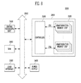
- FIG. 8 is a block diagram illustrating a computing system including the memory system shown in FIG. 7 .
- ‘connected/coupled’ represents that one component is directly coupled to another component or indirectly coupled through another component.
- a singular form may include a plural form as long as it is not specifically mentioned.
- ‘include/comprise’ or ‘including/comprising’ used in the specification represents that one or more components, steps, operations, and elements exist or are added.
- FIG. 1 is a block diagram illustrating a semiconductor memory device 100 according to an embodiment of the present invention.
- the semiconductor memory device 100 may include a voltage generator 150 and an internal circuit 140 .
- the voltage generator may include a control signal generation unit 110 , an operation mode determination circuit 120 , and a bulk voltage generation circuit 130 .
- the control signal generation unit 110 may generate an active chip signal ACTCHIP in response to a chip enable signal CE_N for activating the semiconductor memory device 100 .
- the active chip signal ACTCHIP may transition from a logic high level to a logic low level when the chip enable signal CE_N is deactivated to a logic high level for a predetermined time.
- the semiconductor memory device 100 may determine a standby mode when the deactivation period of the chip enable signal CE_N reaches the predetermined time. For example, the semiconductor memory device 100 may determine the standby mode when the chip enable signal CE_N is deactivated to the logic high level for 10 ⁇ s.
- the operation mode determination circuit 120 may generate an active mode signal ACTIVE_N and a standby mode signal STANDBY_N in response to the chip enable signal CE_N and the active chip signal ACTCHIP.
- the active mode signal ACTIVE_N and the standby mode signal STANDBY_N may have opposite logic levels. For example, when the active mode signal ACTIVE_N is in a logic low level, the standby mode signal STANDBY_N may be in a logic high level. On the other hand, when the active mode signal ACTIVE_N is in a logic high level, the standby mode signal STANDBY_N may be in a logic low level.
- the bulk voltage generation circuit 130 may generate a bulk voltage VCC_BB by using an external power voltage VCCE and an internal power voltage VCCI in response to the active mode signal ACTIVE_N and the standby mode signal STANDBY_N, respectively.
- the bulk voltage generation circuit 130 may generate the bulk voltage VCC_BB by using the internal power voltage VCCI in an active mode in which the active mode signal ACTIVE_N is activated to a logic low level
- the bulk voltage generation circuit 130 may generate the bulk voltage VCC_BB by using the external power voltage VCCE in a standby mode in which the standby mode signal STANDBY_N is activated to a logic low level.
- the external power voltage VCCE may be higher than the internal power voltage VCCI.
- the internal circuit 140 may include a plurality of PMOS transistors and a plurality of NMOS transistors.
- the bulk voltage VCC_BB may be applied to bulks of the PMOS transistors.
- the bulk voltage VCC_BB generated using the internal power voltage VCCI may be applied to the internal circuit 140
- the standby mode the bulk voltage VCC_BB generated using the external power voltage VCCE may be applied the internal circuit 140 .
- FIG. 2 is a detailed diagram of the operation mode determination circuit 120 shown in FIG. 1 .
- the operation mode determination circuit 120 may include a logic unit 122 , a level shifter 121 and an output unit 123 .
- the logic unit 122 may include an inverter IV 1 and a NAND gate ND.
- the output unit 123 may include an inverter IV 2 and a buffer BF.
- the inverter IV 1 may receive and invert the active chip signal ACTCHIP.
- the NAND gate ND may perform a NAND combination of an output signal of the inverter IV 1 and the chip enable signal CE_N.
- the inverter IV 1 and the NAND gate ND may use the internal power voltage VCCI as a power voltage. Therefore, an output signal of the logic unit 122 may have a logic high level corresponding to the internal power voltage VCCI.
- the level shifter 121 may change the logic high level of the output signal of the logic unit 122 from the internal power voltage VCCI to the external power voltage VCCE.
- the inverter IV 2 may invert the signal output from the level shifter 121 to output the active mode signal ACTIVE_N.
- the buffer BF may buffer the signal output from the level shifter 121 to output the standby mode signal STANDBY_N.
- the inverter IV 2 and the buffer BF may use the external power voltage VCCE as a power voltage. Therefore, the active mode signal ACTIVE_N and the standby mode signal STANDBY_N have a logic high level corresponding to the external power voltage VCCE.
- FIG. 3 is a detailed diagram of the bulk voltage generation circuit 130 shown in FIG. 1 .
- the bulk voltage generation circuit 130 may include a first switch unit SW 1 and a second switch unit SW 2 .
- the first switch unit SW 1 may include a PMOS transistor PM 1 connected to the internal power voltage VCCI.
- the PMOS transistor PM 1 may drive the bulk voltage VCC_BB terminal with the internal power voltage VCCI, in response to the active mode signal ACTIVE_N.
- the bulk voltage VCC_BB may be applied to a bulk of the PMOS transistor PM 1 .
- the second switch unit SW 2 may include a PMOS transistor PM 2 coupled to the external power voltage VCCE.
- the PMOS transistor PM 2 may drive the bulk voltage VCC_BB terminal with the external power voltage VCCE, in response to the standby mode signal STANDBY_N.
- the external power voltage VCCE may be applied to a bulk of the PMOS transistor PM 2 .
- the internal power voltage VCCI may be output as the bulk voltage VCC_BB in the active mode.
- the second switch unit SW 2 of the bulk voltage generation circuit 130 the external power voltage VCCE may be output as the bulk voltage VCC_BB in the standby mode.
- the first switch unit SW 1 is deactivated, and the bulk voltage VCC_BB having the external power voltage VCCE may be applied to the bulk of the PMOS transistor PM 1 to prevent a leakage current path from being established in a direction from the bulk voltage VCC_BB to the internal power voltage VCCI.
- FIG. 4 is a circuit diagram of transistors included in the internal circuit 140 shown in FIG. 1 .
- the internal circuit 140 includes a PMOS transistor PM and an NMOS transistor NM.
- the PMOS transistor PM and the NMOS transistor NM may be coupled in series.
- the bulk voltage VCC_BB may be applied to the bulk of the PMOS transistor PM.
- the external power voltage VCCE having a higher voltage than the internal power voltage VCCI may be applied as the bulk voltage VCC_BB, a leakage current path caused by the PMOS transistor PM may be blocked. Therefore, power consumption in the standby mode may be reduced.
- FIG. 5 is a waveform view for describing an operation of the semiconductor memory device 100 shown in FIG. 1 .
- the operation of the semiconductor memory device 100 is described below with reference to FIGS. 1 to 5 .
- the chip enable signal CE_N may keep a logic low level, so that the control signal generation unit 110 may generate the active chip signal ACTCHIP at a logic high level.
- the operation mode determination circuit 120 may activate the active mode signal ACTIVE_N at a logic low level and the standby mode signal STANDBY_N at a logic high level, in response to the chip enable signal CE_N having a logic low level and the active chip signal ACTCHIP having a logic high level.
- the bulk voltage generation circuit 130 may switch and output the internal power voltage VCCI to the bulk voltage VCC_BB terminal in response to the active mode signal ACTIVE_N having the logic low level, and the bulk voltage VCC_BB having the internal power voltage VCCI may be applied to the bulk of the PMOS transistor PM included in the internal circuit 140 .
- the control signal generation unit 110 may deactivate the active chip signal ACTCHIP at a logic low level.
- the operation mode determination circuit 120 may deactivate the active mode signal ACTIVE_N to a logic high level and activate the standby mode signal STANDBY_N to a logic low level, in response to the chip enable signal CE_N having the logic high level and the active chip signal ACTCHIP having the logic low level.
- the bulk voltage generation circuit 130 may switch the external power voltage VCCE to the bulk voltage VCC_BB terminal in response to the standby mode signal STANDBY_N having the logic low level, and the bulk voltage VCC_BB having the external power voltage VCCE may be applied to the bulk of the PMOS transistor PM included in the internal circuit 140 .
- the bulk voltage applied to the PMOS transistor PM in the standby mode may be increased, thereby reducing off-leakage current.
- FIG. 6 is a block diagram illustrating a memory system 1000 including the semiconductor memory device 100 shown in FIG. 1 .
- the memory system 1000 may include the semiconductor memory device 100 and a controller 1100 .
- the semiconductor memory device 100 may be configured and operated in substantially the same manner as described above with reference to FIG. 1 . Thus, a detailed description thereof will be omitted.
- the controller 1100 may be coupled to a host and the semiconductor memory device 100 .
- the controller 1100 may access the semiconductor memory device 100 at the request of the host.
- the controller 1100 may control a read operation, a program operation, an erase operation, and/or a background operation of the semiconductor memory device 100 .
- the controller 1100 may provide an interface between the semiconductor memory device 100 and the host.
- the controller 1100 may drive firmware for controlling the semiconductor memory device 100 .
- the controller 1100 may include a random access memory (RAM) 1110 , a processing unit 1120 , a host interface 1130 , a memory interface 1140 , and an error correction block 1150 .
- the RAM 1110 may be used as operation memory of the processing unit 1120 , a cache memory between the semiconductor memory device 100 and the host, and/or a buffer memory between the semiconductor memory device 100 and the host.
- the processing unit 1120 may control operations of the controller 1100 .
- the host interface 1130 may include a protocol for exchanging data between the host and the controller 1100 .
- the controller 1100 may communicate with the host through one or more various protocols such as a universal serial bus (USB) protocol, a multimedia card (MMC) protocol, a peripheral component interconnection (PCI) protocol, a PCI-express (PCI-E) protocol, an advanced technology attachment (ATA) protocol, a serial-ATA protocol, a parallel-ATA protocol, a small computer small interface (SCSI) protocol, an enhanced small disk interface (ESDI) protocol, an integrated drive electronics (IDE) protocol, a private protocol, etc.
- USB universal serial bus
- MMC multimedia card
- PCI peripheral component interconnection
- PCI-E PCI-express
- ATA advanced technology attachment
- serial-ATA protocol serial-ATA protocol
- parallel-ATA a serial-ATA protocol
- SCSI small computer small interface
- ESDI enhanced small disk interface
- IDE integrated drive electronics
- the memory interface 1140 may interface with the semiconductor memory device 100 .
- the memory interface may include a NAND flash interface or a NOR flash interface.
- the error correction block 1150 may detect and correct errors in data read from the semiconductor memory device 100 by using an error correction code (ECC).
- ECC error correction code
- the controller 1100 and the semiconductor memory device 100 may be integrated in a single semiconductor device.
- the controller 1100 and the semiconductor memory device 100 may be integrated in a single semiconductor device to form a memory card such as a PC card (personal computer memory card international association (PCMCIA)), a compact flash card (CF), a smart media card (SMC), a memory stick, a multimedia card (MMC, RS-MMC or MMCmicro), an SD card (SD, miniSD, micro SD or SDHC), a universal flash storage device (UFS), etc.
- PCMCIA personal computer memory card international association
- CF compact flash card
- SMC smart media card
- MMCmicro multimedia card
- SD Secure Digital
- miniSD miniSD
- micro SD or SDHC universal flash storage device
- UFS universal flash storage device
- the controller 1100 and the semiconductor memory device 100 may be integrated in a single semiconductor device to form a solid state drive (SSD).
- the SSD may include a storage device for storing data in a semiconductor memory device.
- operational rates of the host coupled to the memory system 1000 may be significantly improved.
- the memory system 1000 may be used as one of several elements in various electronic devices such as a computer, an ultra mobile PC (UMPC), a workstation, a net-book, a personal digital assistant (PDA), a portable computer, a web table, a wireless phone, a mobile phone, a smart phone, an e-book, a portable multimedia player (PMP), a portable game machine, a navigation device, a black box, a digital camera, a three-dimensional television, a digital audio recorder, a digital audio player, a digital picture recorder, a digital picture player, a digital video recorder, a digital video player, a device for transmitting/receiving information in wireless environments, devices for home networks, devices for computer networks, devices for telematics networks, an RFID device, other devices for computing systems, etc.
- UMPC ultra mobile PC
- PDA personal digital assistant
- PMP portable multimedia player
- PMP portable game machine
- navigation device a black box
- a digital camera a three-dimensional television
- the semiconductor memory device 100 or the memory system 1000 may be packaged in various forms.
- the semiconductor memory device 100 or the memory system 1000 may be packaged by various methods such as a package on package (PoP), a ball grid array (BGA), a chip scale package (CSP), a plastic leaded chip carrier (PLCC), a plastic dual in line package (PDIP), a die in waffle pack, a die in wafer form, a chip on board (COB), a ceramic dual in line package (CERDIP), a plastic metric quad flat package (MQFP), a thin quad flat package (TQFP), a small outline integrated circuit (SOIC), a shrink small outline package (SSOP), a thin small outline package (TSOP), a system in package (SIP), a multi chip package (MCP), a wafer-level fabricated package (WFP), a wafer-level processed stack package (WSP), etc.
- PoP package on package
- BGA ball grid array
- CSP chip scale package
- PLCC plastic leaded chip
- FIG. 7 is a block diagram illustrating an applied example of the memory system 1000 shown in FIG. 6 .
- a memory system 2000 may include a semiconductor memory device 2100 and a controller 2200 .
- the semiconductor memory device 2100 may include semiconductor memory chips.
- the semiconductor memory chips may be divided into groups.
- FIG. 7 illustrates the groups communicating with the controller 2200 through first to k-th channels CH 1 to CHk.
- Each of the semiconductor memory chips may be configured and operated in substantially the same manner as the semiconductor memory device 100 described above with reference to FIG. 1 .
- Each group may communicate with the controller 2200 through a single common channel.
- the controller 2200 may be configured in substantially the same manner as the controller 1100 described with reference to FIG. 6 , and configured to control the memory chips of the semiconductor memory device 2100 .
- FIG. 8 is a block diagram illustrating a computing system 3000 having the memory system 2000 shown in FIG. 7 .
- the computing system 3000 may include a central processing unit 3100 , a random access memory (RAM) 3200 , a user interface 3300 , a power supply 3400 , a system bus 3500 , and a memory system 2000 .
- a central processing unit 3100 a central processing unit 3100 , a random access memory (RAM) 3200 , a user interface 3300 , a power supply 3400 , a system bus 3500 , and a memory system 2000 .
- RAM random access memory
- the memory system 2000 may be electrically connected to the central processing unit 3100 , the RAM 3200 , the user interface 3300 and the power supply 3400 through the system bus 3500 . Data provided through the user interface 3300 or processed by the central processing unit 3100 may be stored in the memory system 2000 .
- the semiconductor memory device 2100 may be coupled to the system bus 3500 through the controller 2200 . However, the semiconductor memory device 2100 may be directly coupled to the system bus 3500 .
- the central processing unit 3100 and the RAM 3200 may perform functions of the controller 2200 .
- the memory system 2000 shown in FIG. 7 may be included as the memory system 3000 .
- the memory system 2000 may be replaced with the memory system 1000 shown in FIG. 6 .
- the computing system 3000 may include both of the memory systems 1000 and 2000 described above with reference to FIGS. 6 and 7 .
- a leakage current caused by transistors of the semiconductor memory device may be prevented to reduce consumption of standby current.
Abstract
A voltage generator that includes an operation mode determination circuit suitable for determining an active mode or a standby mode based on a chip enable signal to activate an active mode signal or a standby mode signal according to a result of the determination; and a bulk voltage generation circuit outputting a bulk voltage having an internal power voltage when the active mode signal is activated, and outputting the bulk voltage having an external power voltage when the standby mode signal is activated.
Description
The present application claims priority to Korean patent application number 10-2015-0069630, filed on May 19, 2015, the entire disclosure of which is herein incorporated by reference in its entirety.
Field of Invention
Various embodiments relate to an electronic device, and more particularly, to a voltage generator, a semiconductor memory device having the same, and a method of operating the semiconductor memory device.
Description of Related Art
Semiconductor memory devices are typically categorized into volatile memory devices and non-volatile memory devices.
Volatile memory devices perform write and read operations at high speed, but they are unable to retain data stored therein without a constant source of power. Non-volatile memory devices perform write and read operations at relatively low speed, but they may retain their stored data regardless of whether they have a constant source of power. The non-volatile memory devices include Read Only Memory (ROM), Mask ROM (MROM), Programmable ROM (PROM), Erasable Programmable ROM (EPROM), Electrically Erasable and Programmable ROM (EEPROM), flash memory, Phase-change Random Access Memory (PRAM), Magnetic RAM (MRAM), Resistive RAM (RRAM) and Ferroelectric RAM (FRAM). Flash memories may be NOR type or NAND type.
Flash memories have the advantages of both RAM and ROM. That is, flash memories may be freely programmed and erased similar to RAM. Similar to ROM, flash memories may retain stored data even without power. Flash memories have been widely used as the storage media of portable electronic devices such as mobile phones, digital cameras, personal digital assistants (PDAs), and MP3 players.
In semiconductor memory devices, to prevent a latch-up and unstable variations of threshold voltages of MOS transistors caused by the body effect, bulk voltages are to be applied to bulks of PMOS transistors and NMOS transistors within a semiconductor memory device.
Bulk voltages applied to the PMOS transistors and the NMOS transistors can the amount leakage current of PMOS and NMOS transistors that are in the off state, as well as the operating speed of the transistors. In other words, the amount of leakage current and the operating speed of the NMOS transistors may decrease when the bulk voltage is lower than its source terminal voltage. In addition, the amount of leakage current and the operating speed of the PMOS transistors may decrease with bulk voltages that are higher than the voltage of its source terminal.
Various embodiments are directed to a voltage generator capable of reducing the amount of current consumed in a standby mode of a semiconductor memory device, a semiconductor memory device having the same, and a method of operating the semiconductor memory device.
According to an embodiment, a voltage generator may include an operation mode determination circuit suitable for determining an active mode or a standby mode based on a chip enable signal to activate an active mode signal or a standby mode signal according to a result of the determination; and
a bulk voltage generation circuit outputting a bulk voltage having an internal power voltage when the active mode signal is activated, and outputting the bulk voltage having an external power voltage when the standby mode signal is activated.
According to an embodiment, a voltage generator generating an internal power voltage as a bulk voltage in an active mode of the semiconductor memory device and generating an external power voltage as the bulk voltage in a standby mode and an internal circuit including a plurality of transistors being applied with the bulk voltage.
According to an embodiment, a method of operating a semiconductor memory device may include outputting a standby mode signal when a chip enable signal is deactivated for a predetermined time or longer, switching an external power voltage to a bulk voltage in response to the standby mode signal, and applying the bulk voltage to a bulk of a transistor of an internal circuit to block leakage current.
Hereinafter, various exemplary embodiments will be described in detail with reference to the accompanying drawings. In the drawings, thicknesses and lengths of components may be exaggerated for convenience of illustration. In the following description, a detailed explanation of related functions and constitutions may be omitted for simplicity and conciseness. Like reference numerals refer to like elements throughout the specification and drawings.
Furthermore, ‘connected/coupled’ represents that one component is directly coupled to another component or indirectly coupled through another component. In this specification, a singular form may include a plural form as long as it is not specifically mentioned. Furthermore, ‘include/comprise’ or ‘including/comprising’ used in the specification represents that one or more components, steps, operations, and elements exist or are added.
Referring to FIG. 1 , the semiconductor memory device 100 may include a voltage generator 150 and an internal circuit 140. The voltage generator may include a control signal generation unit 110, an operation mode determination circuit 120, and a bulk voltage generation circuit 130.
The control signal generation unit 110 may generate an active chip signal ACTCHIP in response to a chip enable signal CE_N for activating the semiconductor memory device 100. For example, the active chip signal ACTCHIP may transition from a logic high level to a logic low level when the chip enable signal CE_N is deactivated to a logic high level for a predetermined time. In addition, the semiconductor memory device 100 may determine a standby mode when the deactivation period of the chip enable signal CE_N reaches the predetermined time. For example, the semiconductor memory device 100 may determine the standby mode when the chip enable signal CE_N is deactivated to the logic high level for 10 μs.
The operation mode determination circuit 120 may generate an active mode signal ACTIVE_N and a standby mode signal STANDBY_N in response to the chip enable signal CE_N and the active chip signal ACTCHIP. The active mode signal ACTIVE_N and the standby mode signal STANDBY_N may have opposite logic levels. For example, when the active mode signal ACTIVE_N is in a logic low level, the standby mode signal STANDBY_N may be in a logic high level. On the other hand, when the active mode signal ACTIVE_N is in a logic high level, the standby mode signal STANDBY_N may be in a logic low level.
The bulk voltage generation circuit 130 may generate a bulk voltage VCC_BB by using an external power voltage VCCE and an internal power voltage VCCI in response to the active mode signal ACTIVE_N and the standby mode signal STANDBY_N, respectively. For example, the bulk voltage generation circuit 130 may generate the bulk voltage VCC_BB by using the internal power voltage VCCI in an active mode in which the active mode signal ACTIVE_N is activated to a logic low level, and the bulk voltage generation circuit 130 may generate the bulk voltage VCC_BB by using the external power voltage VCCE in a standby mode in which the standby mode signal STANDBY_N is activated to a logic low level. The external power voltage VCCE may be higher than the internal power voltage VCCI.
The internal circuit 140 may include a plurality of PMOS transistors and a plurality of NMOS transistors. The bulk voltage VCC_BB may be applied to bulks of the PMOS transistors. In addition, in the active mode, the bulk voltage VCC_BB generated using the internal power voltage VCCI may be applied to the internal circuit 140, and in the standby mode, the bulk voltage VCC_BB generated using the external power voltage VCCE may be applied the internal circuit 140.
Referring to FIG. 2 , the operation mode determination circuit 120 may include a logic unit 122, a level shifter 121 and an output unit 123. The logic unit 122 may include an inverter IV1 and a NAND gate ND. The output unit 123 may include an inverter IV2 and a buffer BF.
The inverter IV1 may receive and invert the active chip signal ACTCHIP. The NAND gate ND may perform a NAND combination of an output signal of the inverter IV1 and the chip enable signal CE_N. The inverter IV1 and the NAND gate ND may use the internal power voltage VCCI as a power voltage. Therefore, an output signal of the logic unit 122 may have a logic high level corresponding to the internal power voltage VCCI.
The level shifter 121 may change the logic high level of the output signal of the logic unit 122 from the internal power voltage VCCI to the external power voltage VCCE.
The inverter IV2 may invert the signal output from the level shifter 121 to output the active mode signal ACTIVE_N. The buffer BF may buffer the signal output from the level shifter 121 to output the standby mode signal STANDBY_N. The inverter IV2 and the buffer BF may use the external power voltage VCCE as a power voltage. Therefore, the active mode signal ACTIVE_N and the standby mode signal STANDBY_N have a logic high level corresponding to the external power voltage VCCE.
Referring to FIG. 3 , the bulk voltage generation circuit 130 may include a first switch unit SW1 and a second switch unit SW2.
The first switch unit SW1 may include a PMOS transistor PM1 connected to the internal power voltage VCCI. The PMOS transistor PM1 may drive the bulk voltage VCC_BB terminal with the internal power voltage VCCI, in response to the active mode signal ACTIVE_N. The bulk voltage VCC_BB may be applied to a bulk of the PMOS transistor PM1.
The second switch unit SW2 may include a PMOS transistor PM2 coupled to the external power voltage VCCE. The PMOS transistor PM2 may drive the bulk voltage VCC_BB terminal with the external power voltage VCCE, in response to the standby mode signal STANDBY_N. The external power voltage VCCE may be applied to a bulk of the PMOS transistor PM2.
By a switching operation of the first switch unit SW1 of the bulk voltage generation circuit 130, the internal power voltage VCCI may be output as the bulk voltage VCC_BB in the active mode. By a switching operation of the second switch unit SW2 of the bulk voltage generation circuit 130, the external power voltage VCCE may be output as the bulk voltage VCC_BB in the standby mode. In the standby mode, the first switch unit SW1 is deactivated, and the bulk voltage VCC_BB having the external power voltage VCCE may be applied to the bulk of the PMOS transistor PM1 to prevent a leakage current path from being established in a direction from the bulk voltage VCC_BB to the internal power voltage VCCI.
Referring to FIG. 4 , the internal circuit 140 includes a PMOS transistor PM and an NMOS transistor NM.
The PMOS transistor PM and the NMOS transistor NM may be coupled in series.
When the PMOS transistor PM and the NMOS transistor NM are coupled in series, if a signal SIG_B having the internal power voltage VCCI is transferred as signal SIG_C, in response to signal SIG_A having the internal power voltage VCCI, the bulk voltage VCC_BB may be applied to the bulk of the PMOS transistor PM. In the standby mode of the semiconductor memory device 100, since the external power voltage VCCE having a higher voltage than the internal power voltage VCCI may be applied as the bulk voltage VCC_BB, a leakage current path caused by the PMOS transistor PM may be blocked. Therefore, power consumption in the standby mode may be reduced.
The operation of the semiconductor memory device 100 is described below with reference to FIGS. 1 to 5 .
1) Active Mode
In an active mode of the semiconductor memory device 100, the chip enable signal CE_N may keep a logic low level, so that the control signal generation unit 110 may generate the active chip signal ACTCHIP at a logic high level.
The operation mode determination circuit 120 may activate the active mode signal ACTIVE_N at a logic low level and the standby mode signal STANDBY_N at a logic high level, in response to the chip enable signal CE_N having a logic low level and the active chip signal ACTCHIP having a logic high level.
The bulk voltage generation circuit 130 may switch and output the internal power voltage VCCI to the bulk voltage VCC_BB terminal in response to the active mode signal ACTIVE_N having the logic low level, and the bulk voltage VCC_BB having the internal power voltage VCCI may be applied to the bulk of the PMOS transistor PM included in the internal circuit 140.
2) Standby Mode
When the chip enable signal CE_N is applied at a logic high level for a predetermined time ‘A’ or longer immediately before the standby mode of the semiconductor memory device 100 is determined, the control signal generation unit 110 may deactivate the active chip signal ACTCHIP at a logic low level.
The operation mode determination circuit 120 may deactivate the active mode signal ACTIVE_N to a logic high level and activate the standby mode signal STANDBY_N to a logic low level, in response to the chip enable signal CE_N having the logic high level and the active chip signal ACTCHIP having the logic low level.
The bulk voltage generation circuit 130 may switch the external power voltage VCCE to the bulk voltage VCC_BB terminal in response to the standby mode signal STANDBY_N having the logic low level, and the bulk voltage VCC_BB having the external power voltage VCCE may be applied to the bulk of the PMOS transistor PM included in the internal circuit 140.
Therefore, the bulk voltage applied to the PMOS transistor PM in the standby mode may be increased, thereby reducing off-leakage current.
Referring to FIG. 6 , the memory system 1000 may include the semiconductor memory device 100 and a controller 1100.
The semiconductor memory device 100 may be configured and operated in substantially the same manner as described above with reference to FIG. 1 . Thus, a detailed description thereof will be omitted.
The controller 1100 may be coupled to a host and the semiconductor memory device 100. The controller 1100 may access the semiconductor memory device 100 at the request of the host. For example, the controller 1100 may control a read operation, a program operation, an erase operation, and/or a background operation of the semiconductor memory device 100. The controller 1100 may provide an interface between the semiconductor memory device 100 and the host. The controller 1100 may drive firmware for controlling the semiconductor memory device 100.
The controller 1100 may include a random access memory (RAM) 1110, a processing unit 1120, a host interface 1130, a memory interface 1140, and an error correction block 1150. The RAM 1110 may be used as operation memory of the processing unit 1120, a cache memory between the semiconductor memory device 100 and the host, and/or a buffer memory between the semiconductor memory device 100 and the host. The processing unit 1120 may control operations of the controller 1100.
The host interface 1130 may include a protocol for exchanging data between the host and the controller 1100. For example, the controller 1100 may communicate with the host through one or more various protocols such as a universal serial bus (USB) protocol, a multimedia card (MMC) protocol, a peripheral component interconnection (PCI) protocol, a PCI-express (PCI-E) protocol, an advanced technology attachment (ATA) protocol, a serial-ATA protocol, a parallel-ATA protocol, a small computer small interface (SCSI) protocol, an enhanced small disk interface (ESDI) protocol, an integrated drive electronics (IDE) protocol, a private protocol, etc.
The memory interface 1140 may interface with the semiconductor memory device 100. For example, the memory interface may include a NAND flash interface or a NOR flash interface.
The error correction block 1150 may detect and correct errors in data read from the semiconductor memory device 100 by using an error correction code (ECC). The controller 1100 and the semiconductor memory device 100 may be integrated in a single semiconductor device. According to an embodiment of the present invention, the controller 1100 and the semiconductor memory device 100 may be integrated in a single semiconductor device to form a memory card such as a PC card (personal computer memory card international association (PCMCIA)), a compact flash card (CF), a smart media card (SMC), a memory stick, a multimedia card (MMC, RS-MMC or MMCmicro), an SD card (SD, miniSD, micro SD or SDHC), a universal flash storage device (UFS), etc.
The controller 1100 and the semiconductor memory device 100 may be integrated in a single semiconductor device to form a solid state drive (SSD). The SSD may include a storage device for storing data in a semiconductor memory device. When the memory system 1000 is used as an SSD, operational rates of the host coupled to the memory system 1000 may be significantly improved.
In another example, the memory system 1000 may be used as one of several elements in various electronic devices such as a computer, an ultra mobile PC (UMPC), a workstation, a net-book, a personal digital assistant (PDA), a portable computer, a web table, a wireless phone, a mobile phone, a smart phone, an e-book, a portable multimedia player (PMP), a portable game machine, a navigation device, a black box, a digital camera, a three-dimensional television, a digital audio recorder, a digital audio player, a digital picture recorder, a digital picture player, a digital video recorder, a digital video player, a device for transmitting/receiving information in wireless environments, devices for home networks, devices for computer networks, devices for telematics networks, an RFID device, other devices for computing systems, etc.
According to an embodiment, the semiconductor memory device 100 or the memory system 1000 may be packaged in various forms. For example, the semiconductor memory device 100 or the memory system 1000 may be packaged by various methods such as a package on package (PoP), a ball grid array (BGA), a chip scale package (CSP), a plastic leaded chip carrier (PLCC), a plastic dual in line package (PDIP), a die in waffle pack, a die in wafer form, a chip on board (COB), a ceramic dual in line package (CERDIP), a plastic metric quad flat package (MQFP), a thin quad flat package (TQFP), a small outline integrated circuit (SOIC), a shrink small outline package (SSOP), a thin small outline package (TSOP), a system in package (SIP), a multi chip package (MCP), a wafer-level fabricated package (WFP), a wafer-level processed stack package (WSP), etc.
Referring to FIG. 7 , a memory system 2000 may include a semiconductor memory device 2100 and a controller 2200. The semiconductor memory device 2100 may include semiconductor memory chips. The semiconductor memory chips may be divided into groups.
Each group may communicate with the controller 2200 through a single common channel. The controller 2200 may be configured in substantially the same manner as the controller 1100 described with reference to FIG. 6 , and configured to control the memory chips of the semiconductor memory device 2100.
Referring to FIG. 8 , the computing system 3000 may include a central processing unit 3100, a random access memory (RAM) 3200, a user interface 3300, a power supply 3400, a system bus 3500, and a memory system 2000.
The memory system 2000 may be electrically connected to the central processing unit 3100, the RAM 3200, the user interface 3300 and the power supply 3400 through the system bus 3500. Data provided through the user interface 3300 or processed by the central processing unit 3100 may be stored in the memory system 2000.
In FIG. 8 , the semiconductor memory device 2100 may be coupled to the system bus 3500 through the controller 2200. However, the semiconductor memory device 2100 may be directly coupled to the system bus 3500. The central processing unit 3100 and the RAM 3200 may perform functions of the controller 2200.
As illustrated in FIG. 8 , the memory system 2000 shown in FIG. 7 may be included as the memory system 3000. However, the memory system 2000 may be replaced with the memory system 1000 shown in FIG. 6 . According to an embodiment, the computing system 3000 may include both of the memory systems 1000 and 2000 described above with reference to FIGS. 6 and 7 .
According to an embodiment, since a bulk bias is generated using an external power higher than an internal power in a standby mode of a semiconductor memory device, a leakage current caused by transistors of the semiconductor memory device may be prevented to reduce consumption of standby current.
It will be apparent to those skilled in the art that various modifications can be made to the above-described exemplary embodiments of the present invention without departing from the spirit or scope of the invention. Thus, it is intended that the present invention cover all such modifications provided they come within the scope of the appended claims and their equivalents.
Claims (11)
1. A voltage generator, comprising:
an operation mode determination circuit configured to determine an active mode or a standby mode based on a chip enable signal to activate an active mode signal or a standby mode signal according to a result of the determination; and
a bulk voltage generation circuit configured to outputting a bulk voltage having an internal power voltage when the active mode signal is activated, and to outputting the bulk voltage having an external power voltage when the standby mode signal is activated, wherein the operation mode determination circuit comprises:
a logic unit configured to perform a logical combination of the chip enable signal and the active chip signal;
a level shifter configured to change a logic high level of an output signal of the logic unit from the internal power voltage to the external power voltage; and
an output unit configured to buffer an output signal of the level shifter to output as the standby mode signal and to invert the output signal of the level shifter to output as the active mode signal
a control signal generation unit configured to generate an active chip signal, outputted to the operation mode determination circuit, based on the chip enable signal.
2. The voltage generator of claim 1 , wherein the control signal generation unit deactivates the active chip signal when the chip enable signal is deactivated for a predetermined time.
3. The voltage generator of claim 1 , wherein the logic unit uses the internal power voltage as a power voltage, and the output unit uses the external power voltage as a power voltage.
4. The voltage generator of claim 1 , wherein the bulk voltage generation circuit comprises:
a first switching unit configured to switch the internal power voltage to a bulk voltage terminal in response to the active mode signal; and
a second switching unit configured to switch the external power voltage to the bulk voltage terminal in response to the standby mode signal.
5. The voltage generator of claim 4 , wherein the first switching unit includes a PMOS transistor, and the bulk voltage is applied to a bulk of the PMOS transistor.
6. The voltage generator of claim 4 , wherein the second switching unit includes a PMOS transistor, and the external power voltage is applied to a bulk of the PMOS transistor.
7. A semiconductor memory device, comprising:
a voltage generator configured to generate an internal power voltage as a bulk voltage in an active mode of the semiconductor memory device and to generate an external power voltage as the bulk voltage in a standby mode; and
an internal circuit configured to include a plurality of transistors being applied with the bulk voltage,
wherein the voltage generator comprises:
an operation mode determination circuit configured to determine the active mode or the standby mode based on a chip enable signal to activate an active mode signal or a standby mode signal according to a result of the determination; and
a bulk voltage generation circuit configured to output the bulk voltage having an internal power voltage when the active mode signal is activated, and to output the bulk voltage having the external power voltage when the standby mode signal is activated, and wherein the operation mode determination circuit comprises:
a logic unit configured to perform a logical combination of the chip enable signal and the active chip signal;
a level shifter configured to change a logic high level of an output signal of the logic unit from the internal power voltage to the external power voltage;
an output unit configured to buffer an output signal of the level shifter to output as the standby mode signal and to invert the output signal of the level shifter to output as the active mode signal; and
a control signal generation unit configured to generate an active chip signal, outputted to the operation mode determination circuit, based on the chip enable signal.
8. The semiconductor memory device of claim 7 , wherein the control signal generation unit deactivates the active chip signal when the chip enable signal is deactivated for a predetermined time.
9. The semiconductor memory device of claim 7 , wherein the logic unit uses the internal power voltage as a power voltage, and the output unit uses the external power voltage as a power voltage.
10. The semiconductor memory device of claim 7 , wherein the bulk voltage generation circuit comprises:
a first switching unit configured to switch the internal power voltage to a bulk voltage terminal in response to the active mode signal; and
a second switching unit configured to switch the external power voltage to the bulk voltage terminal in response to the standby mode signal.
11. The semiconductor memory device of claim 10 , wherein the first switching unit includes a first PMOS transistor, and the bulk voltage is applied to a bulk of the first PMOS transistor, and
the second switching unit includes a second PMOS transistor, and the external power voltage is applied to a bulk of the second PMOS transistor.
Applications Claiming Priority (2)
| Application Number | Priority Date | Filing Date | Title |
|---|---|---|---|
| KR1020150069630A KR20160136007A (en) | 2015-05-19 | 2015-05-19 | Device for controlling voltage, semiconductor memory device having the same, and method of controlling semiconductor memory device |
| KR10-2015-0069630 | 2015-05-19 |
Publications (2)
| Publication Number | Publication Date |
|---|---|
| US20160343447A1 US20160343447A1 (en) | 2016-11-24 |
| US9607709B2 true US9607709B2 (en) | 2017-03-28 |
Family
ID=57326052
Family Applications (1)
| Application Number | Title | Priority Date | Filing Date |
|---|---|---|---|
| US14/865,562 Active US9607709B2 (en) | 2015-05-19 | 2015-09-25 | Voltage generator, semiconductor memory device having the same, and method of operating semiconductor memory device |
Country Status (3)
| Country | Link |
|---|---|
| US (1) | US9607709B2 (en) |
| KR (1) | KR20160136007A (en) |
| CN (1) | CN106169310B (en) |
Families Citing this family (3)
| Publication number | Priority date | Publication date | Assignee | Title |
|---|---|---|---|---|
| KR102478114B1 (en) * | 2016-08-05 | 2022-12-16 | 에스케이하이닉스 주식회사 | Current break circuit, semiconductor device having the same and operating method thereof |
| KR102461866B1 (en) * | 2018-03-27 | 2022-11-02 | 에스케이하이닉스 주식회사 | Circuit for generating voltage |
| TW202310594A (en) * | 2021-08-19 | 2023-03-01 | 韓商愛思開海力士有限公司 | Method for error handling of an interconnection protocol, controller and storage device |
Citations (5)
| Publication number | Priority date | Publication date | Assignee | Title |
|---|---|---|---|---|
| US6363031B2 (en) * | 1999-11-03 | 2002-03-26 | Cypress Semiconductor Corp. | Circuit, architecture and method for reducing power consumption in a synchronous integrated circuit |
| KR20080004219A (en) | 2006-07-05 | 2008-01-09 | 주식회사 하이닉스반도체 | Device for controlling voltage |
| US7545177B1 (en) * | 2007-03-20 | 2009-06-09 | Xilinx, Inc. | Method and apparatus for leakage current reduction |
| US7920409B1 (en) * | 2007-06-05 | 2011-04-05 | Arizona Board Of Regents For And On Behalf Of Arizona State University | SRAM cell with intrinsically high stability and low leakage |
| US8816754B1 (en) * | 2012-11-02 | 2014-08-26 | Suvolta, Inc. | Body bias circuits and methods |
Family Cites Families (3)
| Publication number | Priority date | Publication date | Assignee | Title |
|---|---|---|---|---|
| KR100610021B1 (en) * | 2005-01-14 | 2006-08-08 | 삼성전자주식회사 | Bit line voltage supplying circuit in semiconductor memory device and voltage supplying method therefor |
| US7372746B2 (en) * | 2005-08-17 | 2008-05-13 | Micron Technology, Inc. | Low voltage sensing scheme having reduced active power down standby current |
| KR102033528B1 (en) * | 2013-03-14 | 2019-11-08 | 에스케이하이닉스 주식회사 | Semiconductor Memory Device For Reducing Standby current |
-
2015
- 2015-05-19 KR KR1020150069630A patent/KR20160136007A/en unknown
- 2015-09-25 US US14/865,562 patent/US9607709B2/en active Active
- 2015-10-16 CN CN201510674366.1A patent/CN106169310B/en active Active
Patent Citations (5)
| Publication number | Priority date | Publication date | Assignee | Title |
|---|---|---|---|---|
| US6363031B2 (en) * | 1999-11-03 | 2002-03-26 | Cypress Semiconductor Corp. | Circuit, architecture and method for reducing power consumption in a synchronous integrated circuit |
| KR20080004219A (en) | 2006-07-05 | 2008-01-09 | 주식회사 하이닉스반도체 | Device for controlling voltage |
| US7545177B1 (en) * | 2007-03-20 | 2009-06-09 | Xilinx, Inc. | Method and apparatus for leakage current reduction |
| US7920409B1 (en) * | 2007-06-05 | 2011-04-05 | Arizona Board Of Regents For And On Behalf Of Arizona State University | SRAM cell with intrinsically high stability and low leakage |
| US8816754B1 (en) * | 2012-11-02 | 2014-08-26 | Suvolta, Inc. | Body bias circuits and methods |
Also Published As
| Publication number | Publication date |
|---|---|
| CN106169310A (en) | 2016-11-30 |
| KR20160136007A (en) | 2016-11-29 |
| CN106169310B (en) | 2020-07-28 |
| US20160343447A1 (en) | 2016-11-24 |
Similar Documents
| Publication | Publication Date | Title |
|---|---|---|
| US9455044B2 (en) | Semiconductor memory device performing program and program verify operation on the memory cell array including pass/fail check on the program operation | |
| CN106340318B (en) | Power-on reset circuit and semiconductor memory device including the same | |
| US9859009B2 (en) | Semiconductor memory device for switching high voltage without potential drop | |
| US9570190B2 (en) | Semiconductor memory device to selectively perform a single sensing operation or a multi-sensing operation | |
| US10163512B2 (en) | Semiconductor device capable of effectively eliminating hot holes in a channel and operating method thereof | |
| US9899065B1 (en) | Power-on reset circuit and semiconductor memory device having the same | |
| KR102475458B1 (en) | Power on reset circuit and semiconductor memory device having the same | |
| US9343118B2 (en) | Voltage regulator and apparatus for controlling bias current | |
| US20150348634A1 (en) | Semiconductor memory device, memory system including the same, and operating method thereof | |
| US9472292B1 (en) | Semiconductor memory device | |
| US9792966B2 (en) | Page buffer and semiconductor memory device including the same | |
| US9607709B2 (en) | Voltage generator, semiconductor memory device having the same, and method of operating semiconductor memory device | |
| US9147484B2 (en) | Semiconductor memory device and operating method thereof | |
| KR101916161B1 (en) | Page buffer, memory device compring the same, and method for operating the device | |
| US10176879B2 (en) | High voltage switch circuit and semiconductor memory device including the same | |
| US9601211B1 (en) | Semiconductor memory device | |
| US9754677B2 (en) | Semiconductor memory device, memory system including the same, and operating method thereof | |
| KR20160136002A (en) | Semiconductor device and operating method thereof | |
| US9607670B2 (en) | Data input circuit and semiconductor memory device including the same | |
| CN105321565B (en) | Active driver and semiconductor device having the same | |
| US10742181B2 (en) | Buffer circuit to adjust signal voltage and memory device having the same | |
| US20170125069A1 (en) | Semiconductor device including multiple planes | |
| US11735275B2 (en) | High voltage switch circuit and semiconductor memory device having the same | |
| KR102601963B1 (en) | Block decorder and semiconductor memory device having the same | |
| KR20160073805A (en) | Semiconductor memory device |
Legal Events
| Date | Code | Title | Description |
|---|---|---|---|
| AS | Assignment |
Owner name: SK HYNIX INC., KOREA, REPUBLIC OF Free format text: ASSIGNMENT OF ASSIGNORS INTEREST;ASSIGNOR:KIM, MIN SU;REEL/FRAME:036658/0094 Effective date: 20150908 |
|
| STCF | Information on status: patent grant |
Free format text: PATENTED CASE |
|
| FEPP | Fee payment procedure |
Free format text: PAYOR NUMBER ASSIGNED (ORIGINAL EVENT CODE: ASPN) |
|
| MAFP | Maintenance fee payment |
Free format text: PAYMENT OF MAINTENANCE FEE, 4TH YEAR, LARGE ENTITY (ORIGINAL EVENT CODE: M1551); ENTITY STATUS OF PATENT OWNER: LARGE ENTITY Year of fee payment: 4 |