US9588902B2 - Flexible page sizes for virtual memory - Google Patents
Flexible page sizes for virtual memory Download PDFInfo
- Publication number
- US9588902B2 US9588902B2 US13/693,146 US201213693146A US9588902B2 US 9588902 B2 US9588902 B2 US 9588902B2 US 201213693146 A US201213693146 A US 201213693146A US 9588902 B2 US9588902 B2 US 9588902B2
- Authority
- US
- United States
- Prior art keywords
- page
- size
- page table
- address
- physical memory
- Prior art date
- Legal status (The legal status is an assumption and is not a legal conclusion. Google has not performed a legal analysis and makes no representation as to the accuracy of the status listed.)
- Active, expires
Links
Images


Classifications
-
- G—PHYSICS
- G06—COMPUTING OR CALCULATING; COUNTING
- G06F—ELECTRIC DIGITAL DATA PROCESSING
- G06F12/00—Accessing, addressing or allocating within memory systems or architectures
- G06F12/02—Addressing or allocation; Relocation
- G06F12/08—Addressing or allocation; Relocation in hierarchically structured memory systems, e.g. virtual memory systems
- G06F12/10—Address translation
- G06F12/1009—Address translation using page tables, e.g. page table structures
-
- G—PHYSICS
- G06—COMPUTING OR CALCULATING; COUNTING
- G06F—ELECTRIC DIGITAL DATA PROCESSING
- G06F2212/00—Indexing scheme relating to accessing, addressing or allocation within memory systems or architectures
- G06F2212/65—Details of virtual memory and virtual address translation
- G06F2212/652—Page size control
Definitions
- Virtual memory may be used when the physical memory of a computer system is not large enough to hold all of the desired content.
- a virtual memory address is used to access the physical memory location where the content is stored.
- the physical memory location may be identified by a physical memory page (by specifying a base address of the physical memory page) and an offset within the physical memory page. The relationship between the virtual memory address and the corresponding physical memory address is stored in a page table.
- the virtual memory page-translation mechanism enables system software to create separate address spaces for each process or application. These address spaces are known as virtual address spaces.
- the system software uses the paging mechanism to selectively map individual pages of physical memory into the virtual address space using a set of hierarchical address-translation tables known collectively as page tables.
- Virtual memory may be implemented with any processor, including, but not limited to, a central processing unit (CPU), a graphics processing unit (GPU), and an accelerated processing unit (APU).
- the page table footprint (size of the page table) to map a large memory space can become significant in size.
- One exemplary system contains 4 KB, 64 KB, and potentially larger page sizes.
- a page table footprint is created that assumes that all page sizes are 4 KB. For example, a non-sparse 16 GB memory mapped using 4 KB pages requires 32 MB of space to store the page table. But if all the pages were 64 KB pages and if 64 KB page table entries (PTEs) could be stored natively in the page table, the page table size could be reduced to 8 MB.
- PTEs 64 KB page table entries
- the virtual memory space is larger than the physical memory of a system, some of the virtual memory might not be mapped (referred to discontiguous regions of mapped memory).
- Using a multiple-layer page table allows a smaller page table footprint by not mapping some areas of the virtual memory.
- the x86 (CPU) processor page table format allows only three sizes of page tables: 4 KB, 2 MB, and 1 GB. To support the 2 MB and 1 GB formats, there is a bit indicating that the next level is not a page table block, but rather another PTE. In contrast, a flat page table means that the entire virtual memory address range would need to be mapped.
- the table may be cached, for example, in a translation look-aside buffer (TLB).
- TLB translation look-aside buffer
- One example GPU virtual memory scheme uses fragments (which may be larger or smaller than a full page in size), which addresses the caching problem (by using larger page sizes), but not the page table footprint problem.
- a method for translating a virtual memory address into a physical memory address includes parsing the virtual memory address into a page directory entry offset, a page table entry offset, and an access offset.
- the page directory entry offset is combined with a virtual memory base address to locate a page directory entry in a page directory block, wherein the page directory entry includes a native page table size field and a page table block base address.
- the page table entry offset and the page table block base address are combined to locate a page table entry, wherein the page table entry includes a physical memory page base address and a size of the physical memory page is indicated by the native page table size field.
- the access offset and the physical memory page base address are combined to determine the physical memory address.
- a processor configured to translate a virtual memory address into a physical memory address includes circuitry configured to parse the virtual memory address into a page directory entry offset, a page table entry offset, and an access offset.
- the processor further includes circuitry configured to: combine the page directory entry offset with a virtual memory base address to locate a page directory entry in a page directory block, wherein the page directory entry includes a native page table size field and a base address of a page table block; combine the page table entry offset and the base address of the page table block to locate a page table entry, wherein the page table entry includes a base address of a physical memory page and a size of the physical memory page is indicated by the native page table size field; and combine the access offset and the base address of the physical memory page to determine the physical memory address.
- a non-transitory computer-readable storage medium storing a set of instructions for execution by a general purpose computer to translate a virtual memory address into a physical memory address, the set of instructions including a parsing code segment and three combining code segments.
- the parsing code segment parses the virtual memory address into a page directory entry offset, a page table entry offset, and an access offset.
- the first combining code segment combines the page directory entry offset with a virtual memory base address to locate a page directory entry in a page directory block, wherein the page directory entry includes a native page table size field and a base address of a page table block.
- the second combining code segment combines the page table entry offset and the base address of the page table block to locate a page table entry, wherein the page table entry includes a base address of a physical memory page and a size of the physical memory page is indicated by the native page table size field.
- the third combining code segment combines the access offset and the base address of the physical memory page to determine the physical memory address.
- a method for determining a number of page table entries needed to address a given virtual address space includes determining a page size of each page table entry pointed to by a page directory entry; determining a page directory entry address space pointed to; and determining the number of page table entries by dividing the page directory entry address space pointed to by the page size of each page table entry.
- a page directory entry for use in translating a virtual memory address into a physical memory address includes a native page table size field, indicating a size of a corresponding physical memory page; and a base address of the physical memory page.
- FIG. 2 is a diagram of an example of determining a physical memory address from a virtual memory address
- FIG. 3 is a diagram of a page directory entry (PDE) format
- FIG. 4 is a diagram of a page table entry (PTE) format
- FIG. 5 is a diagram of an example of determining a physical memory address from a virtual memory address with flexible PTE sizes
- FIG. 6 is a flowchart of a method for converting a virtual memory address to a physical memory address
- FIG. 7 is a flowchart of a method for determining a number of PTEs needed for a given address space.
- FIG. 1 is a block diagram of an example device 100 in which one or more disclosed embodiments may be implemented.
- the device 100 may include, for example, a computer, a gaming device, a handheld device, a set-top box, a television, a mobile phone, or a tablet computer.
- the device 100 includes a processor 102 , a memory 104 , a storage 106 , one or more input devices 108 , and one or more output devices 110 .
- the device 100 may also optionally include an input driver 112 and an output driver 114 . It is understood that the device 100 may include additional components not shown in FIG. 1 .
- the processor 102 may include a central processing unit (CPU), a graphics processing unit (GPU), a CPU and GPU located on the same die, or one or more processor cores, wherein each processor core may be a CPU or a GPU.
- the memory 104 may be located on the same die as the processor 102 , or may be located separately from the processor 102 .
- the memory 104 may include a volatile or non-volatile memory, for example, random access memory (RAM), dynamic RAM, or a cache.
- the storage 106 may include a fixed or removable storage, for example, a hard disk drive, a solid state drive, an optical disk, or a flash drive.
- the input devices 108 may include a keyboard, a keypad, a touch screen, a touch pad, a detector, a microphone, an accelerometer, a gyroscope, a biometric scanner, or a network connection (e.g., a wireless local area network card for transmission and/or reception of wireless IEEE 802 signals).
- the output devices 110 may include a display, a speaker, a printer, a haptic feedback device, one or more lights, an antenna, or a network connection (e.g., a wireless local area network card for transmission and/or reception of wireless IEEE 802 signals).
- the input driver 112 communicates with the processor 102 and the input devices 108 , and permits the processor 102 to receive input from the input devices 108 .
- the output driver 114 communicates with the processor 102 and the output devices 110 , and permits the processor 102 to send output to the output devices 110 . It is noted that the input driver 112 and the output driver 114 are optional components, and that the device 100 will operate in the same manner if the input driver 112 and the output driver 114 are not present.
- the phrase “walking the page table” refers to the process of finding a physical address from a virtual address.
- the virtual address includes a page directory entry (PDE) offset, a page table entry (PTE) offset, and an access offset.
- PDE page directory entry
- PTE page table entry
- the PDE offset is an offset into a page directory block (PDB), which is used to locate the PDE.
- PDE contains the base address of a page table block (PTB).
- the PTE offset is an offset into the PTB, and combined with the base address of the PTB, is used to locate the PTE.
- the PTE contains the base address of the physical memory page.
- the access offset is the offset within the physical memory page, and combined with the base address of the physical memory page, gives the physical address.
- FIG. 2 is a diagram of an example 200 of determining a physical memory address from a virtual memory address.
- the virtual memory address 202 includes a PDE offset 204 , a 4 KB PTE offset 206 , and a 4 KB access offset 208 .
- the example 200 shows two different examples of walking the page table; one example uses solid lines and the letter “a” after the corresponding reference number and the other example uses dashed lines and the letter “b” after the corresponding reference number.
- a PDB 210 contains all of the PDEs.
- a virtual memory identifier (VMID) base address 212 of the PDB 210 is already known to the system.
- the PDE offset 204 combined with the base address 212 of the PDB 210 is used to locate the PDE 214 .
- the PDE 214 contains a base address 222 of a PTB 220 .
- the PTE offset 206 from the virtual address 202 is combined with the base address 222 of the PTB 220 to find the PTE 224 .
- the PTE 224 contains a base address 232 of a physical memory page in a system memory 230 where the information is located.
- the access offset 208 from the virtual address 202 is combined with the base address 232 of the physical memory page to find a memory location 234 where the information is located.
- the page table is constructed so that only one entry is required for each page of mapping.
- the flexible PDE format described below includes a field indicating the native size of the PTEs contained in the PTB. Different PTBs can contain pages of different native sizes. For example, one PTB can point to 4 KB physical memory pages, and a separate PTB can point to 2 MB physical memory pages. This PDE format does not change the page table walking mechanism, but only changes the math of calculating the addresses. This format is easy to implement and is flexible in the way the pages are set up.
- Each PDE stores a pointer to the physical base address of a PTB where the PTEs can be found, and describes the native page size of the PTEs in the PTB. Every PTB maps a constant size of memory that is set once (at boot time), and is referred to as the Native Page Table Size. Programming the PTB to point to a larger memory size allows native PTE sizes to be larger than 2 MB and also reduces the number of PDEs necessary to map the memory.
- each PDB In a GPU implementation, there is a single PDB per running application.
- the base address of each PDB is defined by a 4-bit VMID field, and up to 16 PDBs can be defined per virtual memory layer.
- Bits 39 : 21 of each 64-bit virtual memory address specify the location of a PDE in a PDB block. Therefore, each PDB could have up to 2 19 (512K) 64-bit PDE entries, although the normal case would to be have far fewer PDEs in each block.
- FIG. 3 is a diagram of one implementation of a PDE format 300 .
- the PDE 300 includes a valid bit (V) field 302 , a first group of reserved bits 304 , a physical base address of PTB field 306 , a second group of reserved bits 308 , and a Native Page Table Size field 310 . It is noted that the PDE format 300 is an example of one possible implementation of the PDE format, and that a person skilled in the art could vary the number of bits used to convey similar information.
- the physical base address of PTB field 306 is large enough (in one implementation, this field uses bits 39 : 6 ) to address page sizes larger than 4 KB, so the address space does not need to be 4 KB-aligned, like in x86-type systems. This permits multiple PTBs on a single page, such that multiple PTEs could point to different parts of the same page. This means that a page can be suballocated, and each PTB does not have to be 4 KB-aligned (like in an x86-type system). Without the 4 KB-aligned PTB, any size page can be accessed by using only a two-level page walking mechanism.
- x86-type virtual memory systems use one bit to indicate whether the address is to another PTB or to the physical memory page itself, which may result in needing more than two levels of page walking to address certain page sizes. For example, because of the 4 KB alignment requirement, multiple levels are needed to address the 2 MB and 1 GB page sizes.
- the physical memory page size in the PDE fewer PTEs are needed in the PTB, because each PTE points to a larger physical memory page.
- the PTB contains 512 64-bit PTEs and occupies a 4 KB memory footprint.
- the 4 KB PTB can be shared by up to 16 different PDEs.
- FIG. 4 is a diagram of one implementation of a PTE format 400 .
- the PTE 400 includes a group of protection bits 402 used to control access to the PTE, a fragment field 404 , a 4 KB physical page base address field 406 , and a group of reserved bits 408 . It is noted that the PTE format 400 is an example of one possible implementation of the PTE format, and that a person skilled in the art could vary the number of bits used to convey similar information.
- the PDE Native Page Table Size represents the physical footprint of each PTE pointed to by that PDE, while the PTE fragment size represents the maximum logical address space shared by a collective of similar contiguous PTEs.
- FIG. 5 is a diagram of an example 500 of determining a physical memory address from a virtual memory address with flexible PTE sizes.
- the virtual memory address 502 includes a PDE offset 504 , a PTE offset 506 , and an access offset 508 .
- the example 500 shows two different examples of walking the page table; one example uses solid lines and the letter “a” after the corresponding reference number and the other example uses dashed lines and the letter “b” after the corresponding reference number.
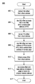
- FIG. 6 is a flowchart of a method 600 for converting a virtual memory address to a physical memory address.
- the PDE offset is extracted from the virtual address (step 602 ).
- the PDE offset is used to locate a PDE in the PDB, which contains the base address of the PTB (step 604 ).
- the PTE offset is extracted from the virtual address (step 606 ).
- the PTE offset and the base address of the PTB are used to locate the PTE, which contains the base address of the physical memory page (step 608 ).
- the access offset is extracted from the virtual address (step 610 ).
- the access offset and the base address of the physical memory page are used to locate the physical address (step 612 ) and the method terminates (step 614 ).
- the PAGE_TABLE_BLOCK_SIZE register field is located in a separate configuration register and is used to determine how much address space is represented by a PDE.
- the PDE address space divided by the PTE page size for that PDE determines how many PTEs are required to represent all of the PDE address space.
Landscapes
- Engineering & Computer Science (AREA)
- Theoretical Computer Science (AREA)
- Physics & Mathematics (AREA)
- General Engineering & Computer Science (AREA)
- General Physics & Mathematics (AREA)
- Memory System Of A Hierarchy Structure (AREA)
Abstract
Description
PTE adress space=2NativePageTableSize×4 KB=29×4 KB=512×4 KB=2 MB
Logical/Physical fragment size in bytes=2(12+fragment)
Number of PTEs=(2 MB×2PAGE _ TABLE _ BLOCK _ SIZE)/(4 KB×2PDE Native Page Table Size).
PTE address space=2Native Page Table Size×4 KB=29×4 KB=512×4 KB=2 MB
Claims (10)
Priority Applications (1)
| Application Number | Priority Date | Filing Date | Title |
|---|---|---|---|
| US13/693,146 US9588902B2 (en) | 2012-12-04 | 2012-12-04 | Flexible page sizes for virtual memory |
Applications Claiming Priority (1)
| Application Number | Priority Date | Filing Date | Title |
|---|---|---|---|
| US13/693,146 US9588902B2 (en) | 2012-12-04 | 2012-12-04 | Flexible page sizes for virtual memory |
Publications (2)
| Publication Number | Publication Date |
|---|---|
| US20140156968A1 US20140156968A1 (en) | 2014-06-05 |
| US9588902B2 true US9588902B2 (en) | 2017-03-07 |
Family
ID=50826687
Family Applications (1)
| Application Number | Title | Priority Date | Filing Date |
|---|---|---|---|
| US13/693,146 Active 2034-12-16 US9588902B2 (en) | 2012-12-04 | 2012-12-04 | Flexible page sizes for virtual memory |
Country Status (1)
| Country | Link |
|---|---|
| US (1) | US9588902B2 (en) |
Cited By (5)
| Publication number | Priority date | Publication date | Assignee | Title |
|---|---|---|---|---|
| US10754795B2 (en) * | 2018-11-26 | 2020-08-25 | Qualcomm Incorporated | MMU assisted address sanitizer |
| EP3757804A1 (en) * | 2019-06-28 | 2020-12-30 | INTEL Corporation | Page tables for granular allocation of memory pages |
| US10908827B2 (en) | 2018-01-02 | 2021-02-02 | Samsung Electronics Co., Ltd. | Semiconductor memory devices, and memory systems and electronic apparatuses having the same |
| US20210157492A1 (en) * | 2018-08-10 | 2021-05-27 | Denso Corporation | Vehicle electronic control system, file transfer control method, computer program product and data structure of specification data |
| US11860793B2 (en) | 2021-04-27 | 2024-01-02 | Samsung Electronics Co., Ltd. | Controller, computing system including the same, and method of creating and searching page table entry for the same |
Families Citing this family (9)
| Publication number | Priority date | Publication date | Assignee | Title |
|---|---|---|---|---|
| US9058268B1 (en) * | 2012-09-20 | 2015-06-16 | Matrox Graphics Inc. | Apparatus, system and method for memory management |
| US10324838B2 (en) | 2017-10-12 | 2019-06-18 | International Business Machines Corporation | Virtually addressable hardware global kernel segment table |
| CN110046053B (en) * | 2019-04-19 | 2021-11-12 | 上海兆芯集成电路有限公司 | Processing system for distributing tasks and access method thereof |
| CN112835820B (en) * | 2019-11-22 | 2025-09-30 | 北京忆芯科技有限公司 | Method and storage device for quickly accessing HMB |
| US11537526B2 (en) | 2020-09-10 | 2022-12-27 | Micron Technology, Inc. | Translating of logical address to determine first and second portions of physical address |
| US11537527B2 (en) * | 2020-12-10 | 2022-12-27 | Micron Technology, Inc. | Dynamic logical page sizes for memory devices |
| GB2604629B (en) * | 2021-03-10 | 2023-06-07 | Imagination Tech Ltd | A computer system and method using a first page table and a second page table |
| CN116185902B (en) * | 2023-04-13 | 2023-08-01 | 阿里云计算有限公司 | Table segmentation method, system, electronic equipment and readable medium |
| US12493560B2 (en) * | 2024-04-18 | 2025-12-09 | Dell Products L.P. | Flexibly sized virtual layer blocks for logical address mapping |
Citations (20)
| Publication number | Priority date | Publication date | Assignee | Title |
|---|---|---|---|---|
| US4410941A (en) * | 1980-12-29 | 1983-10-18 | Wang Laboratories, Inc. | Computer having an indexed local ram to store previously translated virtual addresses |
| US5794228A (en) * | 1993-04-16 | 1998-08-11 | Sybase, Inc. | Database system with buffer manager providing per page native data compression and decompression |
| US5835963A (en) * | 1994-09-09 | 1998-11-10 | Hitachi, Ltd. | Processor with an addressable address translation buffer operative in associative and non-associative modes |
| US6079004A (en) * | 1995-01-27 | 2000-06-20 | International Business Machines Corp. | Method of indexing a TLB using a routing code in a virtual address |
| US6189074B1 (en) * | 1997-03-19 | 2001-02-13 | Advanced Micro Devices, Inc. | Mechanism for storing system level attributes in a translation lookaside buffer |
| US6643759B2 (en) * | 2001-03-30 | 2003-11-04 | Mips Technologies, Inc. | Mechanism to extend computer memory protection schemes |
| US6671791B1 (en) * | 2001-06-15 | 2003-12-30 | Advanced Micro Devices, Inc. | Processor including a translation unit for selectively translating virtual addresses of different sizes using a plurality of paging tables and mapping mechanisms |
| US6823433B1 (en) * | 2001-11-13 | 2004-11-23 | Advanced Micro Devices, Inc. | Memory management system and method for providing physical address based memory access security |
| US20050086650A1 (en) * | 1999-01-28 | 2005-04-21 | Ati International Srl | Transferring execution from one instruction stream to another |
| US20060004983A1 (en) * | 2004-06-30 | 2006-01-05 | Tsao Gary Y | Method, system, and program for managing memory options for devices |
| US20060149919A1 (en) * | 2005-01-05 | 2006-07-06 | Arizpe Arturo L | Method, system, and program for addressing pages of memory by an I/O device |
| US20090077306A1 (en) * | 2006-06-08 | 2009-03-19 | Bitmicro Networks, Inc. | Optimizing memory operations in an electronic storage device |
| US20090172344A1 (en) * | 2007-12-31 | 2009-07-02 | Ed Grochowski | Method, system, and apparatus for page sizing extension |
| US20100235831A1 (en) * | 2009-03-12 | 2010-09-16 | Arend Erich Dittmer | Method for dynamic configuration of virtual machine |
| US20110029961A1 (en) * | 2009-07-31 | 2011-02-03 | Google Inc. | Native code module security for arm instruction set architectures |
| US20110071813A1 (en) * | 2009-09-18 | 2011-03-24 | International Business Machines Corporation | Page Mapped Spatially Aware Emulation of a Computer Instruction Set |
| US20110087858A1 (en) * | 2009-10-08 | 2011-04-14 | Arm Limited | Memory management unit |
| US8041923B2 (en) * | 2008-01-11 | 2011-10-18 | International Business Machines Corporation | Load page table entry address instruction execution based on an address translation format control field |
| US20130246709A1 (en) * | 2012-03-13 | 2013-09-19 | Nvidia Corporation | Translation address cache for a microprocessor |
| US20140019689A1 (en) * | 2012-07-10 | 2014-01-16 | International Business Machines Corporation | Methods of cache preloading on a partition or a context switch |
-
2012
- 2012-12-04 US US13/693,146 patent/US9588902B2/en active Active
Patent Citations (20)
| Publication number | Priority date | Publication date | Assignee | Title |
|---|---|---|---|---|
| US4410941A (en) * | 1980-12-29 | 1983-10-18 | Wang Laboratories, Inc. | Computer having an indexed local ram to store previously translated virtual addresses |
| US5794228A (en) * | 1993-04-16 | 1998-08-11 | Sybase, Inc. | Database system with buffer manager providing per page native data compression and decompression |
| US5835963A (en) * | 1994-09-09 | 1998-11-10 | Hitachi, Ltd. | Processor with an addressable address translation buffer operative in associative and non-associative modes |
| US6079004A (en) * | 1995-01-27 | 2000-06-20 | International Business Machines Corp. | Method of indexing a TLB using a routing code in a virtual address |
| US6189074B1 (en) * | 1997-03-19 | 2001-02-13 | Advanced Micro Devices, Inc. | Mechanism for storing system level attributes in a translation lookaside buffer |
| US20050086650A1 (en) * | 1999-01-28 | 2005-04-21 | Ati International Srl | Transferring execution from one instruction stream to another |
| US6643759B2 (en) * | 2001-03-30 | 2003-11-04 | Mips Technologies, Inc. | Mechanism to extend computer memory protection schemes |
| US6671791B1 (en) * | 2001-06-15 | 2003-12-30 | Advanced Micro Devices, Inc. | Processor including a translation unit for selectively translating virtual addresses of different sizes using a plurality of paging tables and mapping mechanisms |
| US6823433B1 (en) * | 2001-11-13 | 2004-11-23 | Advanced Micro Devices, Inc. | Memory management system and method for providing physical address based memory access security |
| US20060004983A1 (en) * | 2004-06-30 | 2006-01-05 | Tsao Gary Y | Method, system, and program for managing memory options for devices |
| US20060149919A1 (en) * | 2005-01-05 | 2006-07-06 | Arizpe Arturo L | Method, system, and program for addressing pages of memory by an I/O device |
| US20090077306A1 (en) * | 2006-06-08 | 2009-03-19 | Bitmicro Networks, Inc. | Optimizing memory operations in an electronic storage device |
| US20090172344A1 (en) * | 2007-12-31 | 2009-07-02 | Ed Grochowski | Method, system, and apparatus for page sizing extension |
| US8041923B2 (en) * | 2008-01-11 | 2011-10-18 | International Business Machines Corporation | Load page table entry address instruction execution based on an address translation format control field |
| US20100235831A1 (en) * | 2009-03-12 | 2010-09-16 | Arend Erich Dittmer | Method for dynamic configuration of virtual machine |
| US20110029961A1 (en) * | 2009-07-31 | 2011-02-03 | Google Inc. | Native code module security for arm instruction set architectures |
| US20110071813A1 (en) * | 2009-09-18 | 2011-03-24 | International Business Machines Corporation | Page Mapped Spatially Aware Emulation of a Computer Instruction Set |
| US20110087858A1 (en) * | 2009-10-08 | 2011-04-14 | Arm Limited | Memory management unit |
| US20130246709A1 (en) * | 2012-03-13 | 2013-09-19 | Nvidia Corporation | Translation address cache for a microprocessor |
| US20140019689A1 (en) * | 2012-07-10 | 2014-01-16 | International Business Machines Corporation | Methods of cache preloading on a partition or a context switch |
Non-Patent Citations (1)
| Title |
|---|
| (Intel® 64 and IA-32 Architectures Software Developer's Manual vol. 3A: System Programming Guide, Part 1, May 2011). * |
Cited By (6)
| Publication number | Priority date | Publication date | Assignee | Title |
|---|---|---|---|---|
| US10908827B2 (en) | 2018-01-02 | 2021-02-02 | Samsung Electronics Co., Ltd. | Semiconductor memory devices, and memory systems and electronic apparatuses having the same |
| US20210157492A1 (en) * | 2018-08-10 | 2021-05-27 | Denso Corporation | Vehicle electronic control system, file transfer control method, computer program product and data structure of specification data |
| US12399632B2 (en) * | 2018-08-10 | 2025-08-26 | Denso Corporation | Vehicle electronic control system, file transfer control method, computer program product and data structure of specification data |
| US10754795B2 (en) * | 2018-11-26 | 2020-08-25 | Qualcomm Incorporated | MMU assisted address sanitizer |
| EP3757804A1 (en) * | 2019-06-28 | 2020-12-30 | INTEL Corporation | Page tables for granular allocation of memory pages |
| US11860793B2 (en) | 2021-04-27 | 2024-01-02 | Samsung Electronics Co., Ltd. | Controller, computing system including the same, and method of creating and searching page table entry for the same |
Also Published As
| Publication number | Publication date |
|---|---|
| US20140156968A1 (en) | 2014-06-05 |
Similar Documents
| Publication | Publication Date | Title |
|---|---|---|
| US9588902B2 (en) | Flexible page sizes for virtual memory | |
| US10838862B2 (en) | Memory controllers employing memory capacity compression, and related processor-based systems and methods | |
| US9858198B2 (en) | 64KB page system that supports 4KB page operations | |
| US20170177497A1 (en) | Compressed caching of a logical-to-physical address table for nand-type flash memory | |
| US9740621B2 (en) | Memory controllers employing memory capacity and/or bandwidth compression with next read address prefetching, and related processor-based systems and methods | |
| US9465748B2 (en) | Instruction fetch translation lookaside buffer management to support host and guest O/S translations | |
| US20070073996A1 (en) | Virtual memory fragment aware cache | |
| KR102051698B1 (en) | Multiple sets of attribute fields within a single page table entry | |
| US20120297139A1 (en) | Memory management unit, apparatuses including the same, and method of operating the same | |
| KR102281928B1 (en) | Variable Transform Index Buffer (TLB) Indexing | |
| JP6945544B2 (en) | Priority-based access of compressed memory lines in memory in processor-based systems | |
| US20140181461A1 (en) | Reporting access and dirty pages | |
| US9110825B2 (en) | Uncached static short address translation table in the cache coherent computer system | |
| JP2017501504A5 (en) | ||
| US10540290B2 (en) | Method and apparatus for translation lookaside buffer with multiple compressed encodings | |
| US20150154119A1 (en) | Memory allocation and page address translation system and method | |
| KR102865969B1 (en) | Memory configuration that is not a power of 2 | |
| EP3559814B1 (en) | Configurable skewed associativity in a translation lookaside buffer | |
| US9483412B2 (en) | Method and apparatus for reformatting page table entries for cache storage | |
| US20190205264A1 (en) | Memory management unit performance through cache optimizations for partially linear page tables of fragmented memory | |
| US9886380B2 (en) | Method and device of memory space management | |
| US10042562B2 (en) | Apparatus and method for a non-power-of-2 size cache in a first level memory device to cache data present in a second level memory device | |
| WO2018077219A1 (en) | Memory management method and system | |
| US10228991B2 (en) | Providing hardware-based translation lookaside buffer (TLB) conflict resolution in processor-based systems | |
| US20160103766A1 (en) | Lookup of a data structure containing a mapping between a virtual address space and a physical address space |
Legal Events
| Date | Code | Title | Description |
|---|---|---|---|
| AS | Assignment |
Owner name: ADVANCED MICRO DEVICES, INC., CALIFORNIA Free format text: ASSIGNMENT OF ASSIGNORS INTEREST;ASSIGNOR:TERRY, ELENE;REEL/FRAME:029398/0722 Effective date: 20121126 Owner name: ATI TECHNOLOGIES ULC, CANADA Free format text: ASSIGNMENT OF ASSIGNORS INTEREST;ASSIGNOR:PARTAP SINGH RANA, DHIRENDRA;REEL/FRAME:029398/0757 Effective date: 20121121 |
|
| STCF | Information on status: patent grant |
Free format text: PATENTED CASE |
|
| MAFP | Maintenance fee payment |
Free format text: PAYMENT OF MAINTENANCE FEE, 4TH YEAR, LARGE ENTITY (ORIGINAL EVENT CODE: M1551); ENTITY STATUS OF PATENT OWNER: LARGE ENTITY Year of fee payment: 4 |
|
| MAFP | Maintenance fee payment |
Free format text: PAYMENT OF MAINTENANCE FEE, 8TH YEAR, LARGE ENTITY (ORIGINAL EVENT CODE: M1552); ENTITY STATUS OF PATENT OWNER: LARGE ENTITY Year of fee payment: 8 |