US9568774B1 - Liquid crystal composition and method for manufacturing liquid crystal display apparatus including the same - Google Patents
Liquid crystal composition and method for manufacturing liquid crystal display apparatus including the same Download PDFInfo
- Publication number
- US9568774B1 US9568774B1 US15/146,334 US201615146334A US9568774B1 US 9568774 B1 US9568774 B1 US 9568774B1 US 201615146334 A US201615146334 A US 201615146334A US 9568774 B1 US9568774 B1 US 9568774B1
- Authority
- US
- United States
- Prior art keywords
- liquid crystal
- substrate
- tert
- crystal composition
- display apparatus
- Prior art date
- Legal status (The legal status is an assumption and is not a legal conclusion. Google has not performed a legal analysis and makes no representation as to the accuracy of the status listed.)
- Active
Links
- 239000004973 liquid crystal related substance Substances 0.000 title claims abstract description 265
- 239000000203 mixture Substances 0.000 title claims abstract description 106
- 238000000034 method Methods 0.000 title claims abstract description 103
- 238000004519 manufacturing process Methods 0.000 title claims abstract description 55
- 239000000758 substrate Substances 0.000 claims abstract description 194
- 239000000178 monomer Substances 0.000 claims abstract description 98
- 230000001939 inductive effect Effects 0.000 claims abstract description 55
- 239000003999 initiator Substances 0.000 claims abstract description 46
- 230000005684 electric field Effects 0.000 claims abstract description 31
- 238000006116 polymerization reaction Methods 0.000 claims description 39
- -1 azo compound Chemical class 0.000 claims description 35
- 238000007789 sealing Methods 0.000 claims description 27
- 150000001875 compounds Chemical class 0.000 claims description 16
- 239000004342 Benzoyl peroxide Substances 0.000 claims description 10
- OMPJBNCRMGITSC-UHFFFAOYSA-N Benzoylperoxide Chemical compound C=1C=CC=CC=1C(=O)OOC(=O)C1=CC=CC=C1 OMPJBNCRMGITSC-UHFFFAOYSA-N 0.000 claims description 10
- 235000019400 benzoyl peroxide Nutrition 0.000 claims description 10
- CIHOLLKRGTVIJN-UHFFFAOYSA-N tert‐butyl hydroperoxide Chemical compound CC(C)(C)OO CIHOLLKRGTVIJN-UHFFFAOYSA-N 0.000 claims description 10
- 230000000977 initiatory effect Effects 0.000 claims description 7
- KDGNCLDCOVTOCS-UHFFFAOYSA-N (2-methylpropan-2-yl)oxy propan-2-yl carbonate Chemical compound CC(C)OC(=O)OOC(C)(C)C KDGNCLDCOVTOCS-UHFFFAOYSA-N 0.000 claims description 5
- NALFRYPTRXKZPN-UHFFFAOYSA-N 1,1-bis(tert-butylperoxy)-3,3,5-trimethylcyclohexane Chemical compound CC1CC(C)(C)CC(OOC(C)(C)C)(OOC(C)(C)C)C1 NALFRYPTRXKZPN-UHFFFAOYSA-N 0.000 claims description 5
- HSLFISVKRDQEBY-UHFFFAOYSA-N 1,1-bis(tert-butylperoxy)cyclohexane Chemical compound CC(C)(C)OOC1(OOC(C)(C)C)CCCCC1 HSLFISVKRDQEBY-UHFFFAOYSA-N 0.000 claims description 5
- CCNDOQHYOIISTA-UHFFFAOYSA-N 1,2-bis(2-tert-butylperoxypropan-2-yl)benzene Chemical compound CC(C)(C)OOC(C)(C)C1=CC=CC=C1C(C)(C)OOC(C)(C)C CCNDOQHYOIISTA-UHFFFAOYSA-N 0.000 claims description 5
- UICXTANXZJJIBC-UHFFFAOYSA-N 1-(1-hydroperoxycyclohexyl)peroxycyclohexan-1-ol Chemical compound C1CCCCC1(O)OOC1(OO)CCCCC1 UICXTANXZJJIBC-UHFFFAOYSA-N 0.000 claims description 5
- HQOVXPHOJANJBR-UHFFFAOYSA-N 2,2-bis(tert-butylperoxy)butane Chemical compound CC(C)(C)OOC(C)(CC)OOC(C)(C)C HQOVXPHOJANJBR-UHFFFAOYSA-N 0.000 claims description 5
- DMWVYCCGCQPJEA-UHFFFAOYSA-N 2,5-bis(tert-butylperoxy)-2,5-dimethylhexane Chemical compound CC(C)(C)OOC(C)(C)CCC(C)(C)OOC(C)(C)C DMWVYCCGCQPJEA-UHFFFAOYSA-N 0.000 claims description 5
- XMNIXWIUMCBBBL-UHFFFAOYSA-N 2-(2-phenylpropan-2-ylperoxy)propan-2-ylbenzene Chemical compound C=1C=CC=CC=1C(C)(C)OOC(C)(C)C1=CC=CC=C1 XMNIXWIUMCBBBL-UHFFFAOYSA-N 0.000 claims description 5
- RFSCGDQQLKVJEJ-UHFFFAOYSA-N 2-methylbutan-2-yl benzenecarboperoxoate Chemical compound CCC(C)(C)OOC(=O)C1=CC=CC=C1 RFSCGDQQLKVJEJ-UHFFFAOYSA-N 0.000 claims description 5
- FRIBMENBGGCKPD-UHFFFAOYSA-N 3-(2,3-dimethoxyphenyl)prop-2-enal Chemical compound COC1=CC=CC(C=CC=O)=C1OC FRIBMENBGGCKPD-UHFFFAOYSA-N 0.000 claims description 5
- VFXXTYGQYWRHJP-UHFFFAOYSA-N 4,4'-azobis(4-cyanopentanoic acid) Chemical compound OC(=O)CCC(C)(C#N)N=NC(C)(CCC(O)=O)C#N VFXXTYGQYWRHJP-UHFFFAOYSA-N 0.000 claims description 5
- YIVJZNGAASQVEM-UHFFFAOYSA-N Lauroyl peroxide Chemical compound CCCCCCCCCCCC(=O)OOC(=O)CCCCCCCCCCC YIVJZNGAASQVEM-UHFFFAOYSA-N 0.000 claims description 5
- KYIKRXIYLAGAKQ-UHFFFAOYSA-N abcn Chemical compound C1CCCCC1(C#N)N=NC1(C#N)CCCCC1 KYIKRXIYLAGAKQ-UHFFFAOYSA-N 0.000 claims description 5
- YRKCREAYFQTBPV-UHFFFAOYSA-N acetylacetone Natural products CC(=O)CC(C)=O YRKCREAYFQTBPV-UHFFFAOYSA-N 0.000 claims description 5
- LSXWFXONGKSEMY-UHFFFAOYSA-N di-tert-butyl peroxide Chemical compound CC(C)(C)OOC(C)(C)C LSXWFXONGKSEMY-UHFFFAOYSA-N 0.000 claims description 5
- USHAGKDGDHPEEY-UHFFFAOYSA-L potassium persulfate Chemical compound [K+].[K+].[O-]S(=O)(=O)OOS([O-])(=O)=O USHAGKDGDHPEEY-UHFFFAOYSA-L 0.000 claims description 5
- GJBRNHKUVLOCEB-UHFFFAOYSA-N tert-butyl benzenecarboperoxoate Chemical compound CC(C)(C)OOC(=O)C1=CC=CC=C1 GJBRNHKUVLOCEB-UHFFFAOYSA-N 0.000 claims description 5
- SWAXTRYEYUTSAP-UHFFFAOYSA-N tert-butyl ethaneperoxoate Chemical compound CC(=O)OOC(C)(C)C SWAXTRYEYUTSAP-UHFFFAOYSA-N 0.000 claims description 5
- 239000004593 Epoxy Substances 0.000 claims description 3
- PPBRXRYQALVLMV-UHFFFAOYSA-N Styrene Natural products C=CC1=CC=CC=C1 PPBRXRYQALVLMV-UHFFFAOYSA-N 0.000 claims description 3
- 239000012966 redox initiator Substances 0.000 claims description 3
- 229960000834 vinyl ether Drugs 0.000 claims description 3
- OZAIFHULBGXAKX-UHFFFAOYSA-N 2-(2-cyanopropan-2-yldiazenyl)-2-methylpropanenitrile Chemical compound N#CC(C)(C)N=NC(C)(C)C#N OZAIFHULBGXAKX-UHFFFAOYSA-N 0.000 claims 4
- 239000010410 layer Substances 0.000 description 87
- 0 *C=C Chemical compound *C=C 0.000 description 35
- 102100036464 Activated RNA polymerase II transcriptional coactivator p15 Human genes 0.000 description 31
- 101000713904 Homo sapiens Activated RNA polymerase II transcriptional coactivator p15 Proteins 0.000 description 31
- 229910004444 SUB1 Inorganic materials 0.000 description 31
- 229910004438 SUB2 Inorganic materials 0.000 description 21
- 101100311330 Schizosaccharomyces pombe (strain 972 / ATCC 24843) uap56 gene Proteins 0.000 description 21
- 101150018444 sub2 gene Proteins 0.000 description 21
- 238000012719 thermal polymerization Methods 0.000 description 13
- 230000000052 comparative effect Effects 0.000 description 12
- 230000001678 irradiating effect Effects 0.000 description 12
- ZMANZCXQSJIPKH-UHFFFAOYSA-N Triethylamine Chemical compound CCN(CC)CC ZMANZCXQSJIPKH-UHFFFAOYSA-N 0.000 description 9
- 239000003566 sealing material Substances 0.000 description 9
- 238000009413 insulation Methods 0.000 description 8
- 239000004065 semiconductor Substances 0.000 description 7
- 238000003860 storage Methods 0.000 description 7
- RYGMFSIKBFXOCR-UHFFFAOYSA-N Copper Chemical compound [Cu] RYGMFSIKBFXOCR-UHFFFAOYSA-N 0.000 description 6
- WYURNTSHIVDZCO-UHFFFAOYSA-N Tetrahydrofuran Chemical compound C1CCOC1 WYURNTSHIVDZCO-UHFFFAOYSA-N 0.000 description 6
- 230000015572 biosynthetic process Effects 0.000 description 6
- 238000006243 chemical reaction Methods 0.000 description 6
- 239000010949 copper Substances 0.000 description 6
- 239000011159 matrix material Substances 0.000 description 6
- 239000010409 thin film Substances 0.000 description 6
- 239000010408 film Substances 0.000 description 5
- ZOKXTWBITQBERF-UHFFFAOYSA-N Molybdenum Chemical compound [Mo] ZOKXTWBITQBERF-UHFFFAOYSA-N 0.000 description 4
- PXHVJJICTQNCMI-UHFFFAOYSA-N Nickel Chemical compound [Ni] PXHVJJICTQNCMI-UHFFFAOYSA-N 0.000 description 4
- RTAQQCXQSZGOHL-UHFFFAOYSA-N Titanium Chemical compound [Ti] RTAQQCXQSZGOHL-UHFFFAOYSA-N 0.000 description 4
- 229910052802 copper Inorganic materials 0.000 description 4
- 238000010586 diagram Methods 0.000 description 4
- 238000010438 heat treatment Methods 0.000 description 4
- 229910052750 molybdenum Inorganic materials 0.000 description 4
- 239000011733 molybdenum Substances 0.000 description 4
- 238000002161 passivation Methods 0.000 description 4
- 239000002356 single layer Substances 0.000 description 4
- 239000010936 titanium Substances 0.000 description 4
- 229910052719 titanium Inorganic materials 0.000 description 4
- 229910052782 aluminium Inorganic materials 0.000 description 3
- XAGFODPZIPBFFR-UHFFFAOYSA-N aluminium Chemical compound [Al] XAGFODPZIPBFFR-UHFFFAOYSA-N 0.000 description 3
- 230000000903 blocking effect Effects 0.000 description 3
- 239000011248 coating agent Substances 0.000 description 3
- 238000000576 coating method Methods 0.000 description 3
- 239000004020 conductor Substances 0.000 description 3
- 238000010030 laminating Methods 0.000 description 3
- 238000005259 measurement Methods 0.000 description 3
- 238000012986 modification Methods 0.000 description 3
- 230000004048 modification Effects 0.000 description 3
- 229920000642 polymer Polymers 0.000 description 3
- 238000010992 reflux Methods 0.000 description 3
- YLQBMQCUIZJEEH-UHFFFAOYSA-N tetrahydrofuran Natural products C=1C=COC=1 YLQBMQCUIZJEEH-UHFFFAOYSA-N 0.000 description 3
- KQZFLOUQHMJMGC-UHFFFAOYSA-N C=C(C)C(=C)OCCOC(=O)C1=CC=C(OC(=O)C2CCC(C3=CC=C(OC(=O)C(=C)C)C=C3)CC2)C=C1.C=C(C)C(=O)OC1=CC=C(C(C)(C)C2=CC=C(OC(=O)C(=C)C)C=C2)C=C1.C=C(C)C(=O)OC1=CC=C(C2=CC=C(OC(=O)C(=C)C)C=C2)C=C1.C=C(C)C(=O)OC1=CC=C(C2CCC(OC(=O)C(=C)C)CC2)C=C1.C=C(C)C(=O)OC1=CC=C2C=C(OC(=O)C(=C)C)C=CC2=C1.C=C(C)C(=O)OC1CCC(C2CCC(OC(=O)C(=C)C)CC2)CC1.C=C(C)C(=O)OCCOC(=O)C1=CC=C(OC(=O)C2=CC=C(C3=CC=C(OC(=O)C(=C)C)C=C3)C=C2)C=C1.C=C(C)C(=O)OCOC(=O)C(=C)C.C=CC(=O)OC1=CC=C(C2=CC=C(OC(=O)C(=C)C)C=C2)C(F)=C1.C=CC(=O)OCCCCCCOC1=CC=C(C(=O)OC2=CC=C(OC(=O)C3=CC=C(OCCCCCCOC(=O)C=C)C=C3)C(C)=C2)C=C1.C=CC(=O)OCCCCOC1=CC=C(C(=O)OC2=CC=C(OC(=O)C3=CC=C(OCCCCOC(=O)C=C)C=C3)C(C)=C2)C=C1.C=CC(=O)OCCCOC1=CC=C(C(=O)OC2=CC=C(OC(=O)C3=CC=C(OCCCOC(=O)C=C)C=C3)C(C)=C2)C=C1.C=CC(=O)OCCCOC1=CC=C(C(=O)OCCC2=CC=C(OC(=O)C3=CC=C(OCCCOC(=O)C=C)C=C3)C=C2)C=C1 Chemical compound C=C(C)C(=C)OCCOC(=O)C1=CC=C(OC(=O)C2CCC(C3=CC=C(OC(=O)C(=C)C)C=C3)CC2)C=C1.C=C(C)C(=O)OC1=CC=C(C(C)(C)C2=CC=C(OC(=O)C(=C)C)C=C2)C=C1.C=C(C)C(=O)OC1=CC=C(C2=CC=C(OC(=O)C(=C)C)C=C2)C=C1.C=C(C)C(=O)OC1=CC=C(C2CCC(OC(=O)C(=C)C)CC2)C=C1.C=C(C)C(=O)OC1=CC=C2C=C(OC(=O)C(=C)C)C=CC2=C1.C=C(C)C(=O)OC1CCC(C2CCC(OC(=O)C(=C)C)CC2)CC1.C=C(C)C(=O)OCCOC(=O)C1=CC=C(OC(=O)C2=CC=C(C3=CC=C(OC(=O)C(=C)C)C=C3)C=C2)C=C1.C=C(C)C(=O)OCOC(=O)C(=C)C.C=CC(=O)OC1=CC=C(C2=CC=C(OC(=O)C(=C)C)C=C2)C(F)=C1.C=CC(=O)OCCCCCCOC1=CC=C(C(=O)OC2=CC=C(OC(=O)C3=CC=C(OCCCCCCOC(=O)C=C)C=C3)C(C)=C2)C=C1.C=CC(=O)OCCCCOC1=CC=C(C(=O)OC2=CC=C(OC(=O)C3=CC=C(OCCCCOC(=O)C=C)C=C3)C(C)=C2)C=C1.C=CC(=O)OCCCOC1=CC=C(C(=O)OC2=CC=C(OC(=O)C3=CC=C(OCCCOC(=O)C=C)C=C3)C(C)=C2)C=C1.C=CC(=O)OCCCOC1=CC=C(C(=O)OCCC2=CC=C(OC(=O)C3=CC=C(OCCCOC(=O)C=C)C=C3)C=C2)C=C1 KQZFLOUQHMJMGC-UHFFFAOYSA-N 0.000 description 2
- VYZAMTAEIAYCRO-UHFFFAOYSA-N Chromium Chemical compound [Cr] VYZAMTAEIAYCRO-UHFFFAOYSA-N 0.000 description 2
- 229910000881 Cu alloy Inorganic materials 0.000 description 2
- VYPSYNLAJGMNEJ-UHFFFAOYSA-N Silicium dioxide Chemical compound O=[Si]=O VYPSYNLAJGMNEJ-UHFFFAOYSA-N 0.000 description 2
- 229910001069 Ti alloy Inorganic materials 0.000 description 2
- 229910045601 alloy Inorganic materials 0.000 description 2
- 239000000956 alloy Substances 0.000 description 2
- 229910021417 amorphous silicon Inorganic materials 0.000 description 2
- 229910052804 chromium Inorganic materials 0.000 description 2
- 239000011651 chromium Substances 0.000 description 2
- 239000012535 impurity Substances 0.000 description 2
- 239000000463 material Substances 0.000 description 2
- 229910052751 metal Inorganic materials 0.000 description 2
- 239000002184 metal Substances 0.000 description 2
- 229910052759 nickel Inorganic materials 0.000 description 2
- 238000003756 stirring Methods 0.000 description 2
- WFKWXMTUELFFGS-UHFFFAOYSA-N tungsten Chemical compound [W] WFKWXMTUELFFGS-UHFFFAOYSA-N 0.000 description 2
- 229910052721 tungsten Inorganic materials 0.000 description 2
- 239000010937 tungsten Substances 0.000 description 2
- QNFURVAYZOFSFB-UHFFFAOYSA-N 4-(4-hexoxyphenyl)phenol Chemical compound C1=CC(OCCCCCC)=CC=C1C1=CC=C(O)C=C1 QNFURVAYZOFSFB-UHFFFAOYSA-N 0.000 description 1
- NIXOWILDQLNWCW-UHFFFAOYSA-M Acrylate Chemical compound [O-]C(=O)C=C NIXOWILDQLNWCW-UHFFFAOYSA-M 0.000 description 1
- CNRCLPIHPBBDAK-UHFFFAOYSA-N C1CCOC1.C1CCOC1.C=C(C)C(=O)O.C=C(C)C(=O)OC1=NC(OC(=O)C(=C)C)=NC(OC2=CC=C(C3=CC=C(OCCCCCC)C=C3)C=C2)=N1.CCCCCCOC1=CC=C(C2=CC=C(O)C=C2)C=C1.CCCCCCOC1=CC=C(C2=CC=C(OC3=NC(Cl)=NC(Cl)=N3)C=C2)C=C1.ClC1=NC(Cl)=NC(Cl)=N1 Chemical compound C1CCOC1.C1CCOC1.C=C(C)C(=O)O.C=C(C)C(=O)OC1=NC(OC(=O)C(=C)C)=NC(OC2=CC=C(C3=CC=C(OCCCCCC)C=C3)C=C2)=N1.CCCCCCOC1=CC=C(C2=CC=C(O)C=C2)C=C1.CCCCCCOC1=CC=C(C2=CC=C(OC3=NC(Cl)=NC(Cl)=N3)C=C2)C=C1.ClC1=NC(Cl)=NC(Cl)=N1 CNRCLPIHPBBDAK-UHFFFAOYSA-N 0.000 description 1
- MWKGNQULBKGVKF-UHFFFAOYSA-N C=C(C)C(=C)OCCOC(=O)C1=CC=C(OC(=O)C2CCC(C3=CC=C(OC(=O)C(=C)C)C=C3)CC2)C=C1.C=C(C)C(=O)OC1=CC=C(C(C)(C)C2=CC=C(OC(=O)C(=C)C)C=C2)C=C1.C=C(C)C(=O)OC1=CC=C(C2=CC=C(OC(=O)C(=C)C)C=C2)C=C1.C=C(C)C(=O)OC1=CC=C(C2CCC(OC(=O)C(=C)C)CC2)C=C1.C=C(C)C(=O)OC1=CC=C2C=C(OC(=O)C(=C)C)C=CC2=C1.C=C(C)C(=O)OC1CCC(C2CCC(OC(=O)C(=C)C)CC2)CC1.C=C(C)C(=O)OCCOC(=O)C1=CC=C(OC(=O)C2=CC=C(C3=CC=C(OC(=O)C(=C)C)C=C3)C=C2)C=C1.C=C(C)C(=O)OCOC(=O)C(=C)C.C=CC(=O)OC1=CC=C(C2=CC=C(OC(=O)C(=C)C)C=C2)C(F)=C1.C=CC(=O)OCCCCOC1=CC=C(C(=O)OC2=CC=C(OC(=O)C3=CC=C(OCCCCOC(=O)C=C)C=C3)C(C)=C2)C=C1.C=CC(=O)OCCCOC1=CC=C(C(=O)OC2=CC=C(OC(=O)C3=CC=C(OCCCOC(=O)C=C)C=C3)C(C)=C2)C=C1.C=CC(=O)OCCCOC1=CC=C(C(=O)OCCC2=CC=C(OC(=O)C3=CC=C(OCCCOC(=O)C=C)C=C3)C=C2)C=C1 Chemical compound C=C(C)C(=C)OCCOC(=O)C1=CC=C(OC(=O)C2CCC(C3=CC=C(OC(=O)C(=C)C)C=C3)CC2)C=C1.C=C(C)C(=O)OC1=CC=C(C(C)(C)C2=CC=C(OC(=O)C(=C)C)C=C2)C=C1.C=C(C)C(=O)OC1=CC=C(C2=CC=C(OC(=O)C(=C)C)C=C2)C=C1.C=C(C)C(=O)OC1=CC=C(C2CCC(OC(=O)C(=C)C)CC2)C=C1.C=C(C)C(=O)OC1=CC=C2C=C(OC(=O)C(=C)C)C=CC2=C1.C=C(C)C(=O)OC1CCC(C2CCC(OC(=O)C(=C)C)CC2)CC1.C=C(C)C(=O)OCCOC(=O)C1=CC=C(OC(=O)C2=CC=C(C3=CC=C(OC(=O)C(=C)C)C=C3)C=C2)C=C1.C=C(C)C(=O)OCOC(=O)C(=C)C.C=CC(=O)OC1=CC=C(C2=CC=C(OC(=O)C(=C)C)C=C2)C(F)=C1.C=CC(=O)OCCCCOC1=CC=C(C(=O)OC2=CC=C(OC(=O)C3=CC=C(OCCCCOC(=O)C=C)C=C3)C(C)=C2)C=C1.C=CC(=O)OCCCOC1=CC=C(C(=O)OC2=CC=C(OC(=O)C3=CC=C(OCCCOC(=O)C=C)C=C3)C(C)=C2)C=C1.C=CC(=O)OCCCOC1=CC=C(C(=O)OCCC2=CC=C(OC(=O)C3=CC=C(OCCCOC(=O)C=C)C=C3)C=C2)C=C1 MWKGNQULBKGVKF-UHFFFAOYSA-N 0.000 description 1
- WJFYSBQKSGBXEX-UHFFFAOYSA-N C=C(C)C(=O)OC1=NC(OC(=O)C(=C)C)=NC(OC2=CC=C(C3=CC=C(OCCCCCC)C=C3)C=C2)=N1 Chemical compound C=C(C)C(=O)OC1=NC(OC(=O)C(=C)C)=NC(OC2=CC=C(C3=CC=C(OCCCCCC)C=C3)C=C2)=N1 WJFYSBQKSGBXEX-UHFFFAOYSA-N 0.000 description 1
- FQCKIWWAEIOPSD-UHFFFAOYSA-N C=CC(=O)OCCCCCCOC1=CC=C(C(=O)OC2=CC=C(OC(=O)C3=CC=C(OCCCCCCOC(=O)C=C)C=C3)C(C)=C2)C=C1 Chemical compound C=CC(=O)OCCCCCCOC1=CC=C(C(=O)OC2=CC=C(OC(=O)C3=CC=C(OCCCCCCOC(=O)C=C)C=C3)C(C)=C2)C=C1 FQCKIWWAEIOPSD-UHFFFAOYSA-N 0.000 description 1
- RJITTZSOOWNEPB-UHFFFAOYSA-L CC(=O)C(OOC(C(C)=O)C(C)=O)C(C)=O.CC(=O)OO.CC(=O)OOC(C)(C)C.CC(C#N)(CCCC(=O)O)N=NC(C)(C#N)CCC(=O)O.CC(C)(C#N)C=NC(C)(C)C#N.CC(C)(C)OO.CC(C)(C)OOC(=O)C1=CC=CC=C1.CC(C)(C)OOC(C)(C)C.CC(C)(C)OOC(C)(C)C.CC(C)(C)OOC(C)(C)C1=CC=CC=C1.CC(C)(C)OOC1(OOC(C)(C)C)CCCCC1.CC(C)(CCC(C)(C)OOC(C)(C)C)COOC(C)(C)C.CC(C)(OO)C1=CC=CC=C1.CC(C)(OOC(C)(C)C1=CC=CC=C1)C1=CC=CC=C1.CC(C)OC(=O)OOC(C)(C)C.CC1CC(C)(C)CC(OOC(C)(C)C)(OOC(C)(C)C)C1.CCC(C)(C)OOC(=O)C1=CC=CC=C1.CCC(C)(OOC(C)(C)C)OOC(C)(C)C.CCCCCCCCCCCC(=O)OOC(=O)CCCCCCCCCCC.N#CC1(N=NC2(C#N)CCCCC2)CCCCC1.O=C(OOC(=O)C1=CC=CC=C1)C1=CC=CC=C1.O=S(=O)(O[K])OOS(=O)(=O)[K]O.OOC1(OOC2(O)CCCCC2)CCCCC1 Chemical compound CC(=O)C(OOC(C(C)=O)C(C)=O)C(C)=O.CC(=O)OO.CC(=O)OOC(C)(C)C.CC(C#N)(CCCC(=O)O)N=NC(C)(C#N)CCC(=O)O.CC(C)(C#N)C=NC(C)(C)C#N.CC(C)(C)OO.CC(C)(C)OOC(=O)C1=CC=CC=C1.CC(C)(C)OOC(C)(C)C.CC(C)(C)OOC(C)(C)C.CC(C)(C)OOC(C)(C)C1=CC=CC=C1.CC(C)(C)OOC1(OOC(C)(C)C)CCCCC1.CC(C)(CCC(C)(C)OOC(C)(C)C)COOC(C)(C)C.CC(C)(OO)C1=CC=CC=C1.CC(C)(OOC(C)(C)C1=CC=CC=C1)C1=CC=CC=C1.CC(C)OC(=O)OOC(C)(C)C.CC1CC(C)(C)CC(OOC(C)(C)C)(OOC(C)(C)C)C1.CCC(C)(C)OOC(=O)C1=CC=CC=C1.CCC(C)(OOC(C)(C)C)OOC(C)(C)C.CCCCCCCCCCCC(=O)OOC(=O)CCCCCCCCCCC.N#CC1(N=NC2(C#N)CCCCC2)CCCCC1.O=C(OOC(=O)C1=CC=CC=C1)C1=CC=CC=C1.O=S(=O)(O[K])OOS(=O)(=O)[K]O.OOC1(OOC2(O)CCCCC2)CCCCC1 RJITTZSOOWNEPB-UHFFFAOYSA-L 0.000 description 1
- MGUBQUBNVPJSHX-UHFFFAOYSA-L CC(=O)C(OOC(C(C)=O)C(C)=O)C(C)=O.CC(=O)OO.CC(=O)OOC(C)(C)C.CC(C)(C)OO.CC(C)(C)OOC(=O)C1=CC=CC=C1.CC(C)(C)OOC(C)(C)C.CC(C)OC(=O)OOC(C)(C)C.CC1CC(C)(C)CC(OOC(C)(C)C)(OOC(C)(C)C)C1.CCCCCCCCCCCC(=O)OOC(=O)CCCCCCCCCCC.O=S(=O)(O[K])OOS(=O)(=O)[K]O Chemical compound CC(=O)C(OOC(C(C)=O)C(C)=O)C(C)=O.CC(=O)OO.CC(=O)OOC(C)(C)C.CC(C)(C)OO.CC(C)(C)OOC(=O)C1=CC=CC=C1.CC(C)(C)OOC(C)(C)C.CC(C)OC(=O)OOC(C)(C)C.CC1CC(C)(C)CC(OOC(C)(C)C)(OOC(C)(C)C)C1.CCCCCCCCCCCC(=O)OOC(=O)CCCCCCCCCCC.O=S(=O)(O[K])OOS(=O)(=O)[K]O MGUBQUBNVPJSHX-UHFFFAOYSA-L 0.000 description 1
- RNBOAHGLLYQFMF-UHFFFAOYSA-N CC(C#N)(CCCC(=O)O)NNC(C)(C#N)CCC(=O)O.CC(C)(C#N)C=NC(C)(C)C#N.CC(C)(C)OOC(C)(C)C.CC(C)(C)OOC(C)(C)C1=CC=CC=C1.CC(C)(C)OOC1(OOC(C)(C)C)CCCCC1.CC(C)(CCC(C)(C)OOC(C)(C)C)COOC(C)(C)C.CC(C)(OO)C1=CC=CC=C1.CC(C)(OOC(C)(C)C1=CC=CC=C1)C1=CC=CC=C1.CCC(C)(C)OOC(=O)C1=CC=CC=C1.CCC(C)(OOC(C)(C)C)OOC(C)(C)C.N#CC1(N=NC2(C#N)CCCCC2)CCCCC1.O=C(OOC(=O)C1=CC=CC=C1)C1=CC=CC=C1.OOC1(OOC2(O)CCCCC2)CCCCC1 Chemical compound CC(C#N)(CCCC(=O)O)NNC(C)(C#N)CCC(=O)O.CC(C)(C#N)C=NC(C)(C)C#N.CC(C)(C)OOC(C)(C)C.CC(C)(C)OOC(C)(C)C1=CC=CC=C1.CC(C)(C)OOC1(OOC(C)(C)C)CCCCC1.CC(C)(CCC(C)(C)OOC(C)(C)C)COOC(C)(C)C.CC(C)(OO)C1=CC=CC=C1.CC(C)(OOC(C)(C)C1=CC=CC=C1)C1=CC=CC=C1.CCC(C)(C)OOC(=O)C1=CC=CC=C1.CCC(C)(OOC(C)(C)C)OOC(C)(C)C.N#CC1(N=NC2(C#N)CCCCC2)CCCCC1.O=C(OOC(=O)C1=CC=CC=C1)C1=CC=CC=C1.OOC1(OOC2(O)CCCCC2)CCCCC1 RNBOAHGLLYQFMF-UHFFFAOYSA-N 0.000 description 1
- CERQOIWHTDAKMF-UHFFFAOYSA-M Methacrylate Chemical compound CC(=C)C([O-])=O CERQOIWHTDAKMF-UHFFFAOYSA-M 0.000 description 1
- CERQOIWHTDAKMF-UHFFFAOYSA-N Methacrylic acid Chemical compound CC(=C)C(O)=O CERQOIWHTDAKMF-UHFFFAOYSA-N 0.000 description 1
- 239000004642 Polyimide Substances 0.000 description 1
- 229910052581 Si3N4 Inorganic materials 0.000 description 1
- 125000003342 alkenyl group Chemical group 0.000 description 1
- 125000003545 alkoxy group Chemical group 0.000 description 1
- 239000003990 capacitor Substances 0.000 description 1
- 239000003086 colorant Substances 0.000 description 1
- 238000004440 column chromatography Methods 0.000 description 1
- MGNCLNQXLYJVJD-UHFFFAOYSA-N cyanuric chloride Chemical compound ClC1=NC(Cl)=NC(Cl)=N1 MGNCLNQXLYJVJD-UHFFFAOYSA-N 0.000 description 1
- 230000003247 decreasing effect Effects 0.000 description 1
- 230000002542 deteriorative effect Effects 0.000 description 1
- 239000012467 final product Substances 0.000 description 1
- 239000011521 glass Substances 0.000 description 1
- AMGQUBHHOARCQH-UHFFFAOYSA-N indium;oxotin Chemical compound [In].[Sn]=O AMGQUBHHOARCQH-UHFFFAOYSA-N 0.000 description 1
- 229910044991 metal oxide Inorganic materials 0.000 description 1
- 150000004706 metal oxides Chemical class 0.000 description 1
- 230000002093 peripheral effect Effects 0.000 description 1
- 239000004033 plastic Substances 0.000 description 1
- 229920001721 polyimide Polymers 0.000 description 1
- 229920000307 polymer substrate Polymers 0.000 description 1
- 230000000379 polymerizing effect Effects 0.000 description 1
- 238000003825 pressing Methods 0.000 description 1
- 239000010453 quartz Substances 0.000 description 1
- 230000005855 radiation Effects 0.000 description 1
- 230000009257 reactivity Effects 0.000 description 1
- 150000003839 salts Chemical class 0.000 description 1
- HQVNEWCFYHHQES-UHFFFAOYSA-N silicon nitride Chemical compound N12[Si]34N5[Si]62N3[Si]51N64 HQVNEWCFYHHQES-UHFFFAOYSA-N 0.000 description 1
- 229910052814 silicon oxide Inorganic materials 0.000 description 1
- 238000003786 synthesis reaction Methods 0.000 description 1
- YVTHLONGBIQYBO-UHFFFAOYSA-N zinc indium(3+) oxygen(2-) Chemical compound [O--].[Zn++].[In+3] YVTHLONGBIQYBO-UHFFFAOYSA-N 0.000 description 1
- TYHJXGDMRRJCRY-UHFFFAOYSA-N zinc indium(3+) oxygen(2-) tin(4+) Chemical compound [O-2].[Zn+2].[Sn+4].[In+3] TYHJXGDMRRJCRY-UHFFFAOYSA-N 0.000 description 1
Images


Classifications
-
- G—PHYSICS
- G02—OPTICS
- G02F—OPTICAL DEVICES OR ARRANGEMENTS FOR THE CONTROL OF LIGHT BY MODIFICATION OF THE OPTICAL PROPERTIES OF THE MEDIA OF THE ELEMENTS INVOLVED THEREIN; NON-LINEAR OPTICS; FREQUENCY-CHANGING OF LIGHT; OPTICAL LOGIC ELEMENTS; OPTICAL ANALOGUE/DIGITAL CONVERTERS
- G02F1/00—Devices or arrangements for the control of the intensity, colour, phase, polarisation or direction of light arriving from an independent light source, e.g. switching, gating or modulating; Non-linear optics
- G02F1/01—Devices or arrangements for the control of the intensity, colour, phase, polarisation or direction of light arriving from an independent light source, e.g. switching, gating or modulating; Non-linear optics for the control of the intensity, phase, polarisation or colour
- G02F1/13—Devices or arrangements for the control of the intensity, colour, phase, polarisation or direction of light arriving from an independent light source, e.g. switching, gating or modulating; Non-linear optics for the control of the intensity, phase, polarisation or colour based on liquid crystals, e.g. single liquid crystal display cells
- G02F1/133—Constructional arrangements; Operation of liquid crystal cells; Circuit arrangements
- G02F1/1333—Constructional arrangements; Manufacturing methods
- G02F1/1337—Surface-induced orientation of the liquid crystal molecules, e.g. by alignment layers
- G02F1/13378—Surface-induced orientation of the liquid crystal molecules, e.g. by alignment layers by treatment of the surface, e.g. embossing, rubbing or light irradiation
-
- C—CHEMISTRY; METALLURGY
- C09—DYES; PAINTS; POLISHES; NATURAL RESINS; ADHESIVES; COMPOSITIONS NOT OTHERWISE PROVIDED FOR; APPLICATIONS OF MATERIALS NOT OTHERWISE PROVIDED FOR
- C09K—MATERIALS FOR MISCELLANEOUS APPLICATIONS, NOT PROVIDED FOR ELSEWHERE
- C09K19/00—Liquid crystal materials
- C09K19/52—Liquid crystal materials characterised by components which are not liquid crystals, e.g. additives with special physical aspect: solvents, solid particles
- C09K19/54—Additives having no specific mesophase characterised by their chemical composition
- C09K19/56—Aligning agents
-
- G—PHYSICS
- G02—OPTICS
- G02F—OPTICAL DEVICES OR ARRANGEMENTS FOR THE CONTROL OF LIGHT BY MODIFICATION OF THE OPTICAL PROPERTIES OF THE MEDIA OF THE ELEMENTS INVOLVED THEREIN; NON-LINEAR OPTICS; FREQUENCY-CHANGING OF LIGHT; OPTICAL LOGIC ELEMENTS; OPTICAL ANALOGUE/DIGITAL CONVERTERS
- G02F1/00—Devices or arrangements for the control of the intensity, colour, phase, polarisation or direction of light arriving from an independent light source, e.g. switching, gating or modulating; Non-linear optics
- G02F1/01—Devices or arrangements for the control of the intensity, colour, phase, polarisation or direction of light arriving from an independent light source, e.g. switching, gating or modulating; Non-linear optics for the control of the intensity, phase, polarisation or colour
- G02F1/13—Devices or arrangements for the control of the intensity, colour, phase, polarisation or direction of light arriving from an independent light source, e.g. switching, gating or modulating; Non-linear optics for the control of the intensity, phase, polarisation or colour based on liquid crystals, e.g. single liquid crystal display cells
- G02F1/133—Constructional arrangements; Operation of liquid crystal cells; Circuit arrangements
- G02F1/1333—Constructional arrangements; Manufacturing methods
- G02F1/1337—Surface-induced orientation of the liquid crystal molecules, e.g. by alignment layers
- G02F1/13378—Surface-induced orientation of the liquid crystal molecules, e.g. by alignment layers by treatment of the surface, e.g. embossing, rubbing or light irradiation
- G02F1/133788—Surface-induced orientation of the liquid crystal molecules, e.g. by alignment layers by treatment of the surface, e.g. embossing, rubbing or light irradiation by light irradiation, e.g. linearly polarised light photo-polymerisation
-
- G—PHYSICS
- G02—OPTICS
- G02F—OPTICAL DEVICES OR ARRANGEMENTS FOR THE CONTROL OF LIGHT BY MODIFICATION OF THE OPTICAL PROPERTIES OF THE MEDIA OF THE ELEMENTS INVOLVED THEREIN; NON-LINEAR OPTICS; FREQUENCY-CHANGING OF LIGHT; OPTICAL LOGIC ELEMENTS; OPTICAL ANALOGUE/DIGITAL CONVERTERS
- G02F1/00—Devices or arrangements for the control of the intensity, colour, phase, polarisation or direction of light arriving from an independent light source, e.g. switching, gating or modulating; Non-linear optics
- G02F1/01—Devices or arrangements for the control of the intensity, colour, phase, polarisation or direction of light arriving from an independent light source, e.g. switching, gating or modulating; Non-linear optics for the control of the intensity, phase, polarisation or colour
- G02F1/13—Devices or arrangements for the control of the intensity, colour, phase, polarisation or direction of light arriving from an independent light source, e.g. switching, gating or modulating; Non-linear optics for the control of the intensity, phase, polarisation or colour based on liquid crystals, e.g. single liquid crystal display cells
- G02F1/133—Constructional arrangements; Operation of liquid crystal cells; Circuit arrangements
- G02F1/1333—Constructional arrangements; Manufacturing methods
- G02F1/1339—Gaskets; Spacers; Sealing of cells
-
- G—PHYSICS
- G02—OPTICS
- G02F—OPTICAL DEVICES OR ARRANGEMENTS FOR THE CONTROL OF LIGHT BY MODIFICATION OF THE OPTICAL PROPERTIES OF THE MEDIA OF THE ELEMENTS INVOLVED THEREIN; NON-LINEAR OPTICS; FREQUENCY-CHANGING OF LIGHT; OPTICAL LOGIC ELEMENTS; OPTICAL ANALOGUE/DIGITAL CONVERTERS
- G02F1/00—Devices or arrangements for the control of the intensity, colour, phase, polarisation or direction of light arriving from an independent light source, e.g. switching, gating or modulating; Non-linear optics
- G02F1/01—Devices or arrangements for the control of the intensity, colour, phase, polarisation or direction of light arriving from an independent light source, e.g. switching, gating or modulating; Non-linear optics for the control of the intensity, phase, polarisation or colour
- G02F1/13—Devices or arrangements for the control of the intensity, colour, phase, polarisation or direction of light arriving from an independent light source, e.g. switching, gating or modulating; Non-linear optics for the control of the intensity, phase, polarisation or colour based on liquid crystals, e.g. single liquid crystal display cells
- G02F1/133—Constructional arrangements; Operation of liquid crystal cells; Circuit arrangements
- G02F1/1333—Constructional arrangements; Manufacturing methods
- G02F1/1337—Surface-induced orientation of the liquid crystal molecules, e.g. by alignment layers
- G02F1/133776—Surface-induced orientation of the liquid crystal molecules, e.g. by alignment layers having structures locally influencing the alignment, e.g. unevenness
-
- G—PHYSICS
- G02—OPTICS
- G02F—OPTICAL DEVICES OR ARRANGEMENTS FOR THE CONTROL OF LIGHT BY MODIFICATION OF THE OPTICAL PROPERTIES OF THE MEDIA OF THE ELEMENTS INVOLVED THEREIN; NON-LINEAR OPTICS; FREQUENCY-CHANGING OF LIGHT; OPTICAL LOGIC ELEMENTS; OPTICAL ANALOGUE/DIGITAL CONVERTERS
- G02F1/00—Devices or arrangements for the control of the intensity, colour, phase, polarisation or direction of light arriving from an independent light source, e.g. switching, gating or modulating; Non-linear optics
- G02F1/01—Devices or arrangements for the control of the intensity, colour, phase, polarisation or direction of light arriving from an independent light source, e.g. switching, gating or modulating; Non-linear optics for the control of the intensity, phase, polarisation or colour
- G02F1/13—Devices or arrangements for the control of the intensity, colour, phase, polarisation or direction of light arriving from an independent light source, e.g. switching, gating or modulating; Non-linear optics for the control of the intensity, phase, polarisation or colour based on liquid crystals, e.g. single liquid crystal display cells
- G02F1/133—Constructional arrangements; Operation of liquid crystal cells; Circuit arrangements
- G02F1/1333—Constructional arrangements; Manufacturing methods
- G02F1/1341—Filling or closing of cells
Definitions
- the present disclosure relates to a liquid crystal composition including a reactive monomer and to a method for manufacturing a liquid crystal display apparatus including the liquid crystal composition.
- liquid crystal display devices are classified as a twisted nematic mode liquid crystal display apparatus, an in-plane switching mode liquid crystal display apparatus, or a vertical alignment mode liquid crystal display apparatus.
- the vertical alignment mode liquid crystal display apparatus liquid crystal molecules are aligned in a certain direction, and the longitudinal axes of the liquid crystal molecules are vertically aligned with respect to a substrate when an electric field is not applied.
- the vertical alignment mode liquid crystal display apparatus generally has a wide viewing angle and a large contrast ratio.
- the present disclosure provides a method for manufacturing a liquid crystal display apparatus, in which the pretilt angle of liquid crystal molecules may be effectively generated, and by which productivity may be improved.
- An embodiment provides a method for manufacturing a liquid crystal display apparatus including providing a liquid crystal composition between a first substrate and a second substrate facing the first substrate, the liquid crystal composition including liquid crystal molecules, a thermal initiator, and a reactive monomer; applying heat to the liquid crystal composition to form an alignment inducing pattern on the first substrate and on the second substrate; forming an electric field between the first substrate and the second substrate; and providing first ultraviolet rays to the liquid crystal composition.
- the forming of the electric field and the providing of the first ultraviolet rays may be conducted during a same process
- the method may further include providing a sealing layer between the first substrate and the second substrate; and applying heat to the sealing layer.
- the providing of the heat to the liquid crystal composition, and the applying of the heat to the sealing layer may be conducted during a same process.
- the method may further include providing second ultraviolet rays to the liquid crystal composition after providing the first ultraviolet rays.
- the first ultraviolet rays and the second ultraviolet rays may have a wavelength in a same region.
- the thermal initiator may be at least one of an azo compound, a peroxy ester compound, a peroxy dicarbonate compound, an acyl peroxide compound, or a redox initiator.
- the thermal initiator may be at least one of tert-amyl peroxybenzoate, 4,4′-azobis(4-cyanopentanoic acid), 1,1′-azobis(cyanocyclohexane), azobisisbutyronitrile (AIBN), 2,2-bis(tert-butylperoxy)butane, 1,1-bis(tert-butylperoxy)cyclohexane, benzoyl peroxide (BPO), 2,5-bis(tert-butylperoxy)-2,5-dimethylhexane, bis[1-(tert-butylperoxy)-1-methylethyl]benzene, 1,1-bis(tert-butylperoxy)-3,3,5-trimethylcyclohexane, tert-butyl hydroperoxide, tert-butyl peracetate, tert-butyl peroxide, tert-butyl peroxybenzoate, tert-buty
- the reactive monomer may include a polymerization reaction group which polymerizes upon initiation by the thermal initiator, and a vertical alignment inducing group which aligns the liquid crystal molecules.
- the polymerization reaction group may be at least one of
- the reactive monomer may include at least one of an acrylate compound, a methacrylate compound, an epoxy compound, an oxetane compound, a vinyl-ether compound, or a styrene compound.
- the alignment inducing patterns may have a bump shape extruded on the first substrate or on the second substrate.
- a liquid crystal composition includes liquid crystal molecules, a thermal initiator, and a reactive monomer having a polymerization reaction group capable of being polymerized upon initiation by the thermal initiator.
- the reactive monomer may be present in an amount of about 1.0 part by weight to about 1.5 parts by weight per 100 parts by weight of the liquid crystal molecules.
- the thermal initiator may be present in an amount of about 1.0 part by weight to about 3.0 parts by weight per 100 parts by weight of the reactive monomer.
- the thermal initiator may be at least of tert-amyl peroxybenzoate, 4,4′-azobis(4-cyanopentanoic acid), 1,1′-azobis(cyanocyclohexane), azobisisbutyronitrile (AIBN), 2,2-bis(tert-butylperoxy)butane, 1,1-bis(tert-butylperoxy)cyclohexane, benzoyl peroxide (BPO), 2,5-bis(tert-butylperoxy)-2,5-dimethylhexane, bis[1-(tert-butylperoxy)-1-methylethyl]benzene, 1,1-bis(tert-butylperoxy)-3,3,5-trimethylcyclohexane, tert-butyl hydroperoxide, tert-butyl peracetate, tert-butyl peroxide, tert-butyl peroxybenzoate, tert-butyl
- the reactive monomer may be a compound represented by following Formula 1.
- A is a group in Formula 1a:
- X 11 , X 12 , X 22 , and X 32 are each independently a direct bond, —O—, —COO—, or —NH—,
- N 11 to N 31 are each independently a group in Formula 1b:
- R 1 to R 3 are each independently a group in Formula 1c:
- n1 to n3 are each independently 0 or 1.
- the reactive monomer may be a triazole compound represented by Formula 2.
- b and h are each independently an integer from 1 to 20
- a, c, e, f, g, and i are each independently an integer of 0 or 1
- d is an integer from 1 to 3
- each X is independently H, —CH 3 , —(CH 2 ) m CH 3 (where m is an integer from 1 to 20), F, Br, I, —OH, —C 3 H 7 , —NH 2 , or CN, and
- R and R′ are each independently a group in Formula 2a:
- the reactive monomer may be a compound in Formula 3.
- X is H, —CH 3 , —(CH) 2 CH 3 , F, Br, I, —OH, —C 3 H 7 , —NH 2 , or —CN, and n is an integer from 1 to 20.
- the reactive monomer may further include a compound represented by Formula 4.
- each M is independently H, —CH 3 , —(CH 2 ) n CH 3 , F, Br, I, —OH, —C 3 H 7 , —NH 2 , or —CN, n is an integer from 1 to 20, and R 5 is a group in Formula 4b,
- B is a group in Formula 4c, where each n is independently an integer from 1 to 20.
- FIGS. 1 and 2 are flowcharts showing a method for manufacturing a liquid crystal display apparatus according to an embodiment
- FIGS. 3A to 3E are schematic diagrams showing the steps for manufacturing a liquid crystal display apparatus according to an embodiment
- FIG. 4 is a plan view schematically showing one pixel among a plurality of pixels included in a display device manufactured by an embodiment of a method for manufacturing a liquid crystal display apparatus;
- FIG. 5 is a cross-sectional view along line I-I′ in FIG. 4 ;
- FIG. 6 is a diagram illustrating the pretilt angle (°) of a liquid crystal molecule.
- FIG. 7A is graph illustrating the pretilt angle values (°) versus the voltage (V) of an applied electric field in accordance with a Comparative Example and an Example.
- FIG. 7B is graph illustrating the voltage holding ratios (VHR, %) versus the ultraviolet irradiation step in accordance with the Comparative Example and the Example.
- inventive concept now will be described more fully hereinafter with reference to the accompanying drawings, in which various embodiments are shown.
- the inventive concept may be embodied in different forms and may have various modifications, and exemplary embodiments of the inventive concept will be described below in more detail with reference to the accompanying drawings.
- the inventive concept should not be construed as limited to the embodiments set forth herein. Rather, these embodiments should be understood to include modifications, equivalents, or substitutes within the spirit and scope of the inventive concept.
- “About” or “approximately” as used herein is inclusive of the stated value and means within an acceptable range of deviation for the particular value as determined by one of ordinary skill in the art, considering the measurement question and the error associated with measurement of the particular quantity (i.e., the limitations of the measurement system). For example, “about” can mean within one or more standard deviations, or within ⁇ 30%, 20%, 10%, 5% of the stated value.
- Exemplary embodiments are described herein with reference to cross section illustrations that are schematic illustrations of idealized embodiments. As such, variations from the shapes of the illustrations as a result, for example, of manufacturing techniques and/or tolerances, are to be expected. Thus, embodiments described herein should not be construed as limited to the particular shapes of regions as illustrated herein but are to include deviations in shapes that result, for example, from manufacturing. For example, a region illustrated or described as flat may, typically, have rough and/or nonlinear features. Moreover, sharp angles that are illustrated may be rounded. Thus, the regions illustrated in the figures are schematic in nature and their shapes are not intended to illustrate the precise shape of a region and are not intended to limit the scope of the present claims.
- FIG. 1 is a flowchart showing a method for manufacturing a liquid crystal display apparatus according to an embodiment.
- the method for manufacturing a liquid crystal display apparatus may include a step of providing a liquid crystal composition between a first substrate and a second substrate S 110 , a step of applying heat to the liquid crystal composition S 130 , and a step of forming an electric field between the first substrate and the second substrate and providing first ultraviolet rays S 150 .
- a step of removing the applied electric field and providing second ultraviolet rays S 170 may be further included.
- the step of providing a liquid crystal composition S 110 is a step of supplying a liquid crystal composition between a first substrate and a second substrate.
- the liquid crystal composition may include liquid crystal molecules, a thermal initiator, and a reactive monomer.
- the first substrate may be obtained by forming a pixel electrode on a first base substrate.
- the second substrate facing the first substrate may be a substrate including a common electrode layer formed thereon. The first substrate, the second substrate, and the liquid crystal composition of the liquid crystal display apparatus will be explained again hereinafter.
- the step of providing the liquid crystal composition S 110 is a step of providing the liquid crystal composition between a first substrate and a second substrate.
- the liquid crystal composition may include liquid crystal molecules, a thermal initiator, and a reactive monomer.
- pixel electrodes may be formed on the first substrate.
- the second substrate facing the first substrate may be a substrate including a common electrode layer formed thereon. The first substrate, the second substrate, and the liquid crystal composition of the liquid crystal display apparatus will be explained hereinafter.
- a method of providing a liquid crystal display apparatus with liquid crystal molecules may be used.
- the liquid crystal display apparatus may be provided with a liquid crystal composition using a liquid crystal dropping method or a liquid crystal injecting method.
- the embodiment is not limited thereto, and any method capable of providing liquid crystal molecules between a first substrate and a second substrate may be used, without limitation.
- the liquid crystal composition may be applied on at least one of the first substrate or the second substrate prior to combining the first substrate and the second substrate.
- the liquid crystal composition may be provided by dropping the liquid crystal composition on some regions of at least one of the first or the second substrate.
- the liquid crystal composition may then be diffused and distributed across the entire surface of the substrate.
- the liquid crystal composition dropped on regions of the substrate may be diffused and distributed across the surface by aligning, combining, and applying pressure to the first substrate and the second substrate.
- the liquid crystal composition may be diffused so as to be distributed on the entire surface of the display area of the display apparatus.
- the first substrate and the second substrate may be combined prior to injecting the liquid crystal composition therebetween.
- the liquid crystal composition may be injected via a liquid crystal injecting inlet formed between the first substrate and the second substrate.
- the liquid crystal composition may be supplied between the first substrate and the second substrate in a vacuum chamber.
- a step of applying heat to the liquid crystal composition S 130 may be performed.
- the step of applying heat to the liquid crystal composition S 130 may be accomplished by applying heat to the first substrate, the second substrate, and the liquid crystal composition disposed between the first substrate and the second substrate.
- the heating process may be an indirect heating process conducted in a high temperature chamber. However, the heating method is not limited thereto, and the heat may also be directly applied to the first substrate and the second substrate, between which is the liquid crystal composition.
- the step of applying heat to the liquid crystal composition S 130 may include the forming of radicals by the thermal initiator included in the liquid crystal composition, and the formation of alignment inducing patterns on the first substrate and on the second substrate by the polymerization of the reactive monomers.
- An electric field may be formed between the first substrate and the second substrate including the alignment inducing patterns formed thereon.
- the electric field may be formed by the voltage difference between the first substrate and the second substrate.
- the liquid crystal molecules may be aligned at a certain pretilt angle by the alignment inducing patterns formed on the first substrate and on the second substrate.
- the electric field formed between the first substrate and the second substrate may be maintained for a certain time period.
- first ultraviolet rays may be provided at least partially simultaneously or simultaneously. Forming the electric field and the providing of the first ultraviolet rays are conducted during a same process. By exposing the liquid crystal composition between the first substrate and the second substrate to the first ultraviolet rays, the liquid crystal molecules may be stably aligned on the alignment inducing patterns. In addition, by irradiating the first ultraviolet rays, the polymerization degree of the thermally polymerized reactive monomers may increase, and the additional polymerization reaction of any unreacted reactive monomers may be induced. Meanwhile, the electric field formed between the first substrate and the second substrate may be maintained during the provision of the first ultraviolet rays.
- the forming of the electric field between the first substrate and the second substrate, and the providing of the first ultraviolet rays may be conducted in the same apparatus. After pretilting the liquid crystal molecules by applying the electric field and providing the first ultraviolet rays, the pretilt angle of the liquid crystal molecules may be maintained even after the electric field has been removed.
- an additional step of providing second ultraviolet rays S 170 may be further included.
- the second ultraviolet rays may have a wavelength in the same region as that of the first ultraviolet rays.
- the dosage of the second ultraviolet rays may be smaller than the dosage of the first ultraviolet rays. That is, the intensity of the second ultraviolet rays may be weaker than the intensity of the first ultraviolet rays.
- the second ultraviolet rays may be provided after removal of the electric field formed between the first substrate and the second substrate.
- the amount of unreacted residual reactive monomers may be decreased.
- the impurity generation in a liquid crystal layer may be minimized. Accordingly, displaying quality of a display apparatus may be improved and good reliability may be attained.
- FIG. 2 is a flowchart showing a method for manufacturing a liquid crystal display apparatus including a step of providing a sealing material.
- a method for manufacturing a liquid crystal display apparatus may further include a step of providing a sealing layer S 210 and a step of applying heat to the sealing layer S 230 .
- the step of applying the heat to the sealing layer S 230 and the step of applying heat to the liquid crystal composition S 130 may be conducted as separate processes.
- the e first substrate may be provided with the liquid crystal composition and the second substrate may be provided with the sealing layer simultaneously.
- the sealing layer may be provided prior to providing the liquid crystal composition.
- the embodiment is not limited thereto, and the step of applying the heat to the sealing layer (S 230 ) and the step of applying the heat to the liquid crystal composition (S 130 ) may be conducted at least partially simultaneously, simultaneously, or in a consecutive order.
- the step of applying the heat to the sealing layer (S 230 ) and the step of applying the heat to the liquid crystal composition (S 130 ) may be conducted during a same process.
- the step of forming the electric field and providing the first ultraviolet rays S 150 and the step of removing the electric field and providing the second ultraviolet rays S 170 may be conducted by the same method as previously described for the method for preparing the liquid crystal display apparatus described in FIG. 1 .
- the step of combining a first substrate and a second substrate may be conducted after providing the liquid crystal composition.
- the step of providing the liquid crystal may be conducted after combining the first substrate and the second substrate.
- FIGS. 3A to 3E are schematic diagrams showing the manufacturing steps of a liquid crystal display apparatus according to an embodiment.
- FIG. 3A illustrates a step of providing a liquid crystal composition in the manufacture of a liquid crystal display apparatus.
- the liquid crystal display apparatus may be manufactured by including a first substrate SUB 1 , a second substrate SUB 2 facing the first substrate SUB 1 , a liquid crystal composition LM disposed between the first substrate SUB 1 and the second substrate SBU 2 , and a sealing layer SL.
- the liquid crystal composition LM and the sealing layer SL are provided on the first substrate SUB 1 , however the embodiment is not limited thereto, and the liquid crystal composition LM and the sealing layer SL may be provided on different substrates from each other.
- the sealing layer SL may be formed by applying an uncured sealing material to the first substrate SUB 1 .
- the sealing material may be an attaching member fixing the first substrate and the second substrate and may be cured at high temperatures.
- the sealing layer SL may be formed between the first substrate SUB 1 and the second substrate SUB 2 at a certain predetermined thickness, and the sealing layer SL thus formed may have a thickness corresponding to a cell gap in the liquid crystal display apparatus.
- the sealing layer may be provided on the second substrate.
- the embodiment is not limited thereto, and the liquid crystal composition and the sealing layer may be provided on the same substrate or on different substrates.
- the liquid crystal composition LM is provided on a portion of the substrate SUB 1 .
- the liquid crystal composition LM may be provided on the first substrate SUB 1 and diffused across the surface to fill to a portion up to where the sealing layer SL is formed.
- FIG. 3B is an illustration of a state in which the liquid crystal composition LM has been provided between the first substrate SUB 1 and the second substrate SUB 2 , and the first substrate SUB 1 and the second substrate SBU 2 are aligned and combined.
- the sealing layer SL may be disposed in a peripheral region of the first substrate SUB 1 and the second substrate SUB 2 for fixing the first substrate SUB 1 and the second substrate SUB 2 .
- FIG. 3C illustrates a step of applying heat to a liquid crystal composition.
- the polymerization of the reactive monomers RM may occur due to the application of the heat, and alignment inducing patterns ALN 1 and ALN 2 may be formed on the first substrate SUB 1 and the second substrate SUB 2 , respectively.
- Liquid crystal molecules LC may be vertically aligned and disposed by the alignment inducing patterns ALN 1 and ALN 2 .
- the alignment inducing patterns ALN 1 and ALN 2 may be extruded on each substrate and may be formed as bump shapes.
- the alignment inducing patterns ALN 1 and ALN 2 may be formed on the sides of the first substrate SUB 1 and the second substrate SUB 2 which face one another.
- FIG. 3C the cross-section of the alignment inducing patterns ALN 1 and ALN 2 in a thickness direction of a liquid crystal layer is shown to be triangular in shape, however the shape of the alignment inducing patterns ALN 1 and ALN 2 is not limited thereto.
- the alignment inducing patterns ALN 1 and ALN 2 may be formed in a random pattern on the first substrate SUB 1 and the second substrate SUB 2 .
- the size of the alignment inducing patterns ALN 1 and ALN 2 may be the same or may be different from each other.
- the step of applying heat to the liquid crystal composition illustrated in FIG. 3C may be a step of applying heat to the sealing layer to cure the sealing material. That is, the step of applying (i.e. providing) heat may be a seal bake process for curing the sealing material.
- the seal bake process for curing the sealing material and the polymerization of the reactive monomers in the liquid crystal composition may be conducted simultaneously or partially simultaneously.
- the seal bake process is conducted when a sealing layer is provided to fix two substrates together during manufacturing of the liquid crystal display apparatus. Accordingly, in an embodiment, the efficiency of a process for the manufacture of a liquid crystal display apparatus may be improved by conducting the polymerization reaction using the seal bake process without adding a separate heating process for thermal polymerization of the reactive monomers.
- a liquid crystal display apparatus manufactured by the disclosed method for manufacturing a liquid crystal display apparatus does not include an alignment layer, which is different from a prior art liquid crystal display apparatus
- the forming step of an alignment layer may be omitted in the manufacturing process. That is, of the formation of an alignment layer, including the steps of coating of an alignment film on a substrate to form an alignment film, pseudo-curing, and main-curing of the coated alignment film, may be omitted.
- a photo polymerization method may be used to form alignment inducing patterns from the reactive monomers on the substrate rather than the thermal polymerization method disclosed in exemplary embodiments.
- a step of applying first irradiation to the reactive monomers to initiate polymerization, and a step of applying second irradiation of ultraviolet rays to the alignment inducing patterns formed by the photo polymerization of the reactive monomers may be conducted.
- the second irradiation of ultraviolet rays may be conducted while applying an electric field to the liquid crystal molecules.
- the second irradiation corresponds to a process of irradiating ultraviolet rays to fix the alignment inducing patterns formed by the polymerization reaction and to fix the liquid crystal molecules.
- the first photo polymerization process may be omitted. Accordingly, a separate apparatus for photo polymerization is not required by the methods disclosed herein, and as a result, productivity may be improved by conducting the seal bake process and the thermal polymerization process simultaneously.
- the temperature and applying time of the heat provided to the liquid crystal composition may be changed based upon the type of thermal initiator included in the liquid crystal composition.
- the heat provided for the polymerization reaction may be selected in consideration of the reactivity of the thermal initiator and storage stability.
- the polymerization reaction may be conducted at a temperature from about 70° C. to about 150° C., however the reaction temperature is not limited thereto.
- the thermal polymerization of the reactive monomers may be conducted simultaneously with the seal bake process at the curing temperature of the sealing material, for example, at a temperature of about 100° C. to about 120° C.
- FIG. 3D illustrates a step of forming an electric field between the first substrate SUB 1 and the second substrate SUB 2 and providing first ultraviolet rays R 1 .
- an electric field may be formed between the first substrate SUB 1 and the second substrate SUB 2 .
- the applied electric field pretilts the liquid crystal molecules LC thus formed.
- the first ultraviolet rays R 1 may be provided to the liquid crystal composition.
- the step of forming the electric field between the first substrate SUB 1 and the second substrate SUB 2 , and the step of providing first ultraviolet rays to the first substrate SUB 1 and the second substrate SUB 2 with the liquid crystal composition disposed therebetween, may be conducted simultaneously.
- the liquid crystal molecules may be aligned at a pretilt angle of a certain degree with respect to the substrate.
- the polymerization of unreacted reactive monomers may be additionally conducted. Meanwhile, by providing the first ultraviolet rays, the liquid crystal molecules with the pretilt angle may be stably aligned adjacent to the alignment inducing patterns.
- FIG. 3E illustrates a step of removing the electric field formed between the first substrate SUB 1 and the second substrate SUB 2 and providing second ultraviolet rays R 2 .
- the additional reaction of the unreacted reactive monomer may be conducted, and the polymerization degree of a polymer produced by the polymerization reaction of the reactive monomer may increase.
- the step of providing the second ultraviolet rays R 2 may be conducted in a state where the electric filed formed between the first substrate SUB 1 and the second substrate SUB 2 formed during providing the first ultraviolet rays is removed.
- the second ultraviolet rays may be ultraviolet rays having a wavelength in the same region as the wavelength of the first ultraviolet rays.
- the step of irradiating the second ultraviolet rays is used to remove unreacted materials in a liquid crystal layer, and the intensity of the second ultraviolet rays may be weaker than that of the first ultraviolet rays.
- the alignment inducing patterns may be formed on the substrate by a thermal polymerization method, and the step of forming an alignment layer in a prior art method for manufacturing a liquid crystal display apparatus may be replaced therewith. Since the thermal polymerization process may be simultaneously conducted with the curing process of the sealing layer, the additional prior art process of irradiating ultraviolet rays to form the alignment inducing patterns is not required. In an embodiment of the disclosed method for manufacturing a liquid crystal display apparatus, the same display quality and reliability may be obtained as that of a prior art liquid crystal display apparatus provided with the alignment layer, and productivity may be also improved.
- the liquid crystal display apparatus provided by the exemplary method for manufacturing a liquid crystal display apparatus may be a super vertical alignment (SVA) mode display apparatus.
- SVA super vertical alignment
- the embodiment is not limited thereto, and may be used in a vertical alignment mode or an in-plane switching mode liquid crystal display apparatus.
- the display quality of the display apparatus may be evaluated by measuring black levels.
- a black mode display apparatus manufactured using the method for manufacturing a liquid crystal display apparatus according to an embodiment was confirmed to have similar black levels when compared to a prior art display apparatus in which liquid crystal molecules are aligned by forming an alignment layer. From the results, the alignment inducing patterns formed by thermally polymerizing the reactive monomers using a thermal initiator may maintain the stable alignment of liquid crystal molecules and may be a replacement for an alignment layer.
- the thermal initiator may be at least one of an azo compound, a peroxyester compound, a peroxy dicarbonate compound, and an acyl peroxide compound.
- the thermal initiator may be a redox initiator.
- the thermal initiator may be at least one of the compounds in Formula 5.
- the reactive monomer included in the liquid crystal composition may include a polymerization reaction group which may be polymerized upon initiation by the thermal initiator, and a vertical alignment inducing group aligning liquid crystal molecules.
- the group for a polymerization reaction may be at least one of
- the reactive monomer included in the liquid crystal composition may include at least one of an acrylate compound, a methacrylate compound, an epoxy compound, an oxetane compound, a vinyl-ether compound, or a styrene compound.
- FIGS. 4 and 5 illustrate a portion of a liquid crystal display apparatus manufactured by a method for manufacturing a liquid crystal display apparatus according to an embodiment.
- FIG. 4 is a plan view showing a portion of a pixel in a liquid crystal display apparatus
- FIG. 5 is a cross-sectional view of a liquid crystal display apparatus taken along line I-I′ in FIG. 4 .
- one pixel PX connected to one gate line among gate lines GL and one data line among data lines DL is shown in FIGS. 4 and 5 , however the embodiment is not limited thereto.
- one gate line and one data line may be connected with a plurality of pixels, or a plurality of gate lines and a plurality of data lines may be connected with one pixel.
- the gate lines GL may be extended in a first direction DR 1 .
- the gate line may be formed on a first base substrate.
- the data lines DL may be extended in a second direction DR 2 crossing the gate lines GL and the first direction DR 1 .
- Each of the pixels PX may include a thin film transistor TFT, a pixel electrode PE connected with the thin film transistor TFT, and a storage electrode part (not shown).
- the thin film transistor TFT may include a gate electrode GE, a gate insulation layer GI, a semiconductor pattern SM, a source electrode SE, and a drain electrode DE.
- the storage electrode part may further include a storage line SLn extended in the first direction DR 1 , and a first branched electrode LSLn and a second branched electrode RSLn, branched from the storage line SLn and extending in the second direction DR 2 .
- the gate electrode GE may be extruded from the gate lines GL or be provided on a portion of the gate lines GL.
- the gate electrode GE may be formed using a metal.
- the gate electrode GE may be formed using nickel, chromium, molybdenum, aluminum, titanium, copper, tungsten, or an alloy thereof.
- the gate electrode GE may be formed as a single layer or a multilayer.
- the gate electrode GE may be a triple layer obtained by laminating molybdenum, aluminum, and molybdenum one by one, or a double layer obtained by laminating titanium and copper one by one.
- the gate electrode GE may be a single layer of an alloy of titanium and copper.
- the semiconductor pattern SM is provided on the gate insulation layer GI.
- the semiconductor pattern SM is provided on the gate electrode GE with the gate insulation layer GI therebetween.
- a partial region of the semiconductor pattern SM is overlapped with the gate electrode GE.
- the semiconductor pattern SM includes an active pattern (not shown) provided on the gate insulation layer GI and an ohmic contact layer (not shown) formed on the active pattern.
- the active pattern may be formed using an amorphous silicon thin film, and the ohmic contact layer may be formed using an n + amorphous silicon thin film.
- the ohmic contact layer makes an ohmic contact between the active pattern and the source electrode SE and the drain electrode DE, respectively.
- the source electrode SE is branched from the data line DL.
- the source electrode SE is formed on the ohmic contact layer and is partially overlapped with the gate electrode GE.
- the drain electrode DE is provided apart from the source electrode SE with the semiconductor pattern SM therebetween.
- the drain electrode DE is formed on the ohmic contact layer and is partially overlapped with the gate electrode GE.
- the source electrode SE and the drain electrode DE may be formed using nickel, chromium, molybdenum, aluminum, titanium, copper, tungsten, or an alloy thereof.
- the source electrode SE and the drain electrode DE may be formed as a single layer or a multilayer using a metal.
- the source electrode SE and the drain electrode DE may be a double layer obtained by laminating titanium and copper one by one, or may be a single layer formed by using an alloy of titanium and copper.
- the upper surface of the active pattern between the source electrode SE and the drain electrode DE is exposed and becomes a channel part forming a conductive channel between the source electrode SE and the drain electrode DE according to the application of a voltage to the gate electrode GE.
- the source electrode SE and the drain electrode DE are overlapped with the semiconductor layer SM at the region other than the channel part formed between the source electrode SE and the drain electrode DE.
- the pixel electrode PE is connected to the drain electrode DE with a passivation layer PSV therebetween.
- the pixel electrode PE is partially overlapped with the storage line SLn, the first and second branch electrodes LSLn and RSLn to form a storage capacitor.
- the passivation layer PSV covers the source electrode SE, the drain electrode DE, the channel part, and the gate insulation layer GI, and has a contact hole CH exposing a portion of the drain electrode DE.
- the passivation layer PSV may be formed of a material including, for example, silicon nitride or silicon oxide.
- the pixel electrode PE is electrically connected to the drain electrode DE through the contact hole CH formed in the passivation layer PSV.
- the pixel electrode PE may be formed using a transparent conductive material. Particularly, the pixel electrode PE may be formed using a transparent conductive oxide.
- the transparent conductive oxide includes indium tin oxide (ITO), indium zinc oxide (IZO), indium tin zinc oxide (ITZO), and the like.
- the liquid crystal display apparatus includes a first substrate SUB 1 , a second substrate SUB 2 facing the first substrate SUB 1 , and a liquid crystal layer LCL provided between the first substrate and the second substrate.
- the gate insulation layer GI is provided on the front of the first base substrate BS 1 and covers the gate lines GL.
- Alignment inducing patterns ALN 1 and ALN 2 may be formed on the first substrate and the second substrate, respectively. The alignment inducing patterns ALN 1 and ALN 2 allow the liquid crystal molecules to be provided with a pretilt angle between the first substrate and the second substrate.
- the second substrate SUB 2 includes a second base substrate BS 2 , a color filter CF, a black matrix BM, and a common electrode CE.
- the second base substrate BS 2 may be a polymer substrate, a plastic substrate, a glass substrate, or a quartz substrate.
- the second base substrate BS 2 may be a transparent insulation substrate.
- the second base substrate may be flexible or rigid.
- the color filter CF is provided on the second base substrate BS 2 and provides colors.
- the color filter CF is included in the second substrate SUB 2 , however the embodiment is not limited thereto.
- the color filter CF may be included in the first substrate SUB 1 .
- the position of the black matrix BM corresponds to a blocking region of the first substrate SUB 1 .
- the blocking region may be defined as a region in which the data lines DL, the thin film transistor TFT, and the gate lines GL are formed.
- the black matrix BM is formed in the blocking region to prevent light leakage.
- the black matrix BM is included in the second substrate SUB 2 , however the black matrix BM may be included in the first substrate SUB 1 , without limitation. Even though not shown, an insulation layer may be formed on the color filter CF and the black matrix BM.
- the common electrode CE is provided on the second base substrate BS 2 and forms an electric field with the pixel electrode PE to drive the liquid crystal layer LCL.
- the common electrode CE is included in the second substrate SUB 2 , however the embodiment is not limited thereto.
- the common electrode CE may be included in the first substrate SUB 1 .
- the common electrode CE may be formed using a transparent conductive material.
- the transparent conductive material may be a conductive metal oxide such as ITO, IZO, ITZO, etc.
- alignment inducing patterns ALN 2 may be disposed on the common electrode CE of the second base substrate BS 2 .
- a liquid crystal layer LCL including liquid crystal molecules is provided between the first substrate SUB 1 and the second substrate SUB 2 .
- the liquid crystal layer LCL may be provided in which liquid crystal molecules having dielectric anisotropy are aligned.
- reactive monomers may be included in the liquid crystal layer.
- the liquid crystal molecules are not limited and may be any commonly used liquid crystal molecules. For example, alkenyl liquid crystal molecules and alkoxy liquid crystal molecules may be used.
- the liquid crystal molecules LC used in an embodiment may have a negative dielectric anisotropy, however in another embodiment, they may have a positive dielectric anisotropy, without limitation.
- FIG. 6 is a diagram illustrating the alignment position of a liquid crystal molecule disposed on the first substrate.
- FIG. 6 may illustrate a liquid crystal molecule LC aligned with a pretilt angle on the first substrate SUB 1 .
- a liquid crystal molecule with a pretilt angle is shown and the alignment inducing patterns are omitted.
- a pretilt angle PT is formed by a first imaginary straight line NL extending along one side of the first substrate SUB 1 , and a second imaginary straight line L 11 extending along the major axis of the liquid crystal molecule LC.
- the pretilt angle PT of the liquid crystal molecule LC measured in an embodiment may be an average value or a typical value of the pretilt angle of each liquid crystal molecule.
- the pretilt angle of the liquid crystal molecule may be from about 80 degrees to about 89 degrees.
- the pretilt angle of the liquid crystal aligned by the alignment inducing patterns may be from about 87 degrees to about 89 degrees.
- a liquid crystal composition including liquid crystal molecules, a thermal initiator, and a reactive monomer having a polymerization reaction group capable of being polymerized upon initiation by the thermal initiator, may be used.
- the reactive monomer may be present in an amount of about 1.0 part by weight to about 3.0 parts by weight per 100 parts by weight of the liquid crystal molecules.
- the thermal initiator may be present in an amount of about 1.0 part by weight to about 10 parts by weight per 100 parts by weight of the reactive monomer.
- the thermal initiator may be present in an amount of about 1.0 part by weight to about 3.0 parts by weight per 100 parts by weight of the reactive monomer.
- the amount of the thermal initiator with respect to the reactive monomer is less than about 1.0 part by weight, the amount of radicals produced for a polymerization reaction may be small, and a polymerization reaction rate may be too slow. If the amount of the thermal initiator is less than about 1.0 part by weight, the formation of alignment inducing patterns may not be easy.
- the amount of the thermal initiator is greater than 3.0 parts by weight with respect to the amount of the reactive monomer, residual thermal initiator present after the polymerization reaction is completed may function as impurities.
- radical formation due to the thermal initiator may become excessive, and the polymerization degree of a polymer formed from the reactive monomer may not increase, thereby deteriorating mechanical properties of the alignment inducing patterns.
- the thermal initiator in the liquid crystal composition may be at least one of tert-amyl peroxybenzoate, 4,4′-azobis(4-cyanopentanoic acid), 1,1′-azobis(cyanocyclohexane), azobisisbutyronitrile (AIBN), 2,2-bis(tert-butylperoxy)butane, 1,1-bis(tert-butylperoxy)cyclohexane, benzoyl peroxide (BPO), 2,5-bis(tert-butylperoxy - )-2,5-dimethylhexane, bis[1-(tert-butylperoxy)-1-methylethyl]benzene, 1,1-bis(tert-butylperoxy)-3,3,5-trimethylcyclohexane, tert-butyl hydroperoxide, tert-butyl peracetate, tert-butyl peroxide, tert-butyl peroxybenzo
- the thermal initiator may be at least one of the compounds represented in Formula 5.
- the thermal initiator may be selected based upon the thermal polymerization conditions.
- BPO or AIBN may be selected as the thermal initiator.
- the liquid crystal composition may include a reactive monomer represented by the following Formula 1.
- a core part “A” may be a group in Formula 1a.
- X 11 , X 12 , X 22 , and X 32 are each independently a direct bond, —O—, —COO—, or —NH—, and N 11 , N 21 , and N 31 are each independently a group in Formula 1b.
- R 1 to R 3 are each independently a group in Formula 1c, and n1 to n3 may be each independently 0 or 1.
- two of the three reactive groups linked to the core part “A” may be a reaction group having a group capable of being polymerized to form alignment inducing patterns, while the remaining one group may be a group including a vertical alignment inducing group capable of aligning liquid crystal molecules.
- the reactive monomer in the liquid crystal composition may be represented by Formula 2.
- the reactive monomer represented by Formula 2 may be a triazole compound.
- b and h are each independently an integer from 1 to 20
- a, c, e, f, g, and i are each independently an integer of 0 or 1
- d is an integer from 1 to 3
- X is H, —CH 3 , —(CH 2 ) m CH 3 (where m is an integer from 1 to 20)
- R and R′ are each independently a group in Formula 2a.
- the reactive monomer represented by Formula 2 may be a compound in Formula 2-1.
- the reactive monomer may be one of the compounds in Formula 3.
- the reactive monomer represented by Formula 3 may be a compound having a polymerization group of acrylate or methacrylate at both terminals thereof.
- the liquid crystal composition may further include a reactive monomer represented by Formula 4 in addition to the reactive monomers of Formulae 1, 2, and 3.
- the reactive monomer represented by Formula 4 has a single group available for a polymerization reaction and may be used to improve the vertical alignment properties of liquid crystal molecules.
- VA may be a group in Formula 4a.
- VA may be a vertical alignment inducing group facilitating the vertical alignment of liquid crystal molecules.
- each M is independently H, —CH 3 , —(CH 2 ) n CH 3 , F, Br, I, —OH, —C 5 H 7 , —NH 2 , or —CN, and each n is independently an integer from 1 to 20.
- R is a group in Formula 4b
- B is a group in Formula 4c, where each n is independently an integer from 1 to 20.
- the reactive monomer represented by Formula 1 is referred to as a first reactive monomer
- the reactive monomer represented by Formula 2 is referred to as a second reactive monomer
- the reactive monomer represented by Formula 3 is referred to as a third reactive monomer.
- at least one of the first reactive monomer, the second reactive monomer, or the third reactive monomer may be included in the liquid crystal composition.
- the reactive monomer represented by Formula 4 is referred to as a fourth reactive monomer.
- the fourth reactive monomer and at least one of the first reactive monomer, the second reactive monomer, or the third reactive monomer may be included in the liquid crystal composition together.
- the solubility of the reactive monomers with respect to the liquid crystal molecules may increase. Due to the increased solubility, a greater amount of the reactive monomer may be used in the liquid crystal composition as compared to a composition including only one kind of reactive monomer. According to the increase of the amount of the reactive monomer included in the liquid crystal composition, the formation of the alignment inducing patterns may become easy, thereby improving the alignment property of the liquid crystal molecules.
- the amount of the fourth reactive monomer may be smaller than the amount of each of the first to third reactive monomers.
- the fourth reactive monomer is a reactive monomer including a single group available for a polymerization reaction, and has lower degree of polymerization when compared to that of the first to third reactive monomers. Accordingly, the fourth reactive monomer may act as an alignment inducing group to facilitate the alignment of liquid crystal molecules rather than forming alignment inducing patterns.
- the above-described method for manufacturing a liquid crystal display apparatus is used to prepare an Example liquid crystal display.
- a prior art method for manufacturing a liquid crystal display apparatus including an alignment layer is used to prepare a Comparative Example.
- the liquid crystal composition of the Example includes liquid crystal molecules, a thermal initiator, and a reactive monomer.
- the thermal initiator is BPO
- the reactive monomer is a compound represented by the following Formula 1-1.
- the reactive monomer represented by Formula 1-1 may be prepared by the following Reaction 1.
- the Example liquid crystal display apparatus is manufactured using a liquid crystal composition including the reactive monomer of Formula 1-1 prepared by Reaction 1.
- the Comparative Example corresponds to a liquid crystal display apparatus having alignment layers on a first substrate and a second substrate, different from the Example.
- the alignment layer used in the Comparative Example may be formed by coating an alignment solution on a substrate and thermally curing the alignment solution to form an alignment layer.
- the alignment layer thus formed may be an alignment layer including a polyimide polymer.
- the same kind of liquid crystal molecules were used, and the manufacturing conditions of the display apparatus were the same except for the forming or not forming of the alignment layer.
- FIGS. 7A and 7B are graphs comparing a pretilt angle and a voltage holding ratio (VHR) of liquid crystal display apparatuses manufactured by methods for manufacturing liquid crystal display apparatuses in accordance with the Example and the Comparative Example.
- VHR voltage holding ratio
- FIG. 7A is a graph illustrating the pretilt angle values of liquid crystal molecules versus the voltage values of an applied electric field.
- liquid crystal molecules were aligned using alignment inducing patterns formed on a substrate without an alignment layer, and the pretilt angle of about 87 degrees to about 89 degrees was obtained. This value is almost the same as that for the Comparative Example in which an alignment layer is formed. Accordingly, it the liquid crystals may be aligned to have a stable pretilt angle by only forming the alignment inducing patterns, that is, without the alignment layer.
- the alignment inducing patterns were formed by a thermal polymerization process using the liquid crystal composition including the thermal initiator.
- one ultraviolet irradiating process step may be omitted, and productivity may be improved when compared to a method for forming alignment inducing patterns by photo polymerization (Comparative Example).
- the quality of a display apparatus manufactured by the Example manufacturing method was good since the pretilt values of the liquid crystal molecules is essentially the same as for the Comparative Example.
- FIG. 7B is a graph illustrating a voltage holding ratio (VHR, %) versus the ultraviolet radiation step in accordance with the Example and the Comparative Example.
- the abscissa represents each step of irradiating ultraviolet rays in the manufacturing steps of a liquid crystal display apparatus, and includes no irradiating of ultraviolet rays (unirradiated), irradiating first ultraviolet rays (first), and irradiating first and second ultraviolet rays (second).
- the liquid crystal composition in an embodiment may include liquid crystal molecules, a thermal initiator, and a reactive monomer capable of being polymerized upon initiation by the thermal initiator, and may form alignment inducing patterns capable of aligning liquid crystal molecules.
- the thermal polymerization process and a seal bake process curing a sealing material may be conducted simultaneously. Accordingly, one step of irradiating ultraviolet rays may be removed when compared to a process of forming alignment inducing patterns using a photo polymerization reaction.
- the exemplary method of forming the alignment inducing patterns from the reactive monomers does not include forming the alignment layer, the steps of coating of an alignment layer and a curing process may be omitted, and the productivity of a liquid crystal display apparatus may be improved.
- the liquid crystal molecules may be stably pretilted and aligned by the alignment inducing patterns formed by the method for manufacturing a liquid crystal display apparatus according to an embodiment, and the same or better display quality may be obtained when compared to a prior art liquid crystal display apparatus including an alignment layer.
- a liquid crystal composition including a thermal initiator is used, and alignment inducing patterns may be formed by a thermal polymerization method. Accordingly, liquid crystal molecules may have stable pretilt angle using only the alignment inducing patterns formed by the thermal polymerization method without the need for an alignment layer.
- a curing process of a sealing material provided for combining upper and lower substrates of a liquid crystal display apparatus, and a forming process of alignment inducing patterns may be conducted simultaneously, and the productivity of the manufacturing process of the liquid crystal display apparatus may be improved.
Landscapes
- Physics & Mathematics (AREA)
- Chemical & Material Sciences (AREA)
- Nonlinear Science (AREA)
- Crystallography & Structural Chemistry (AREA)
- Mathematical Physics (AREA)
- General Physics & Mathematics (AREA)
- Optics & Photonics (AREA)
- Spectroscopy & Molecular Physics (AREA)
- Engineering & Computer Science (AREA)
- Materials Engineering (AREA)
- Organic Chemistry (AREA)
- Liquid Crystal (AREA)
Abstract
Description


and
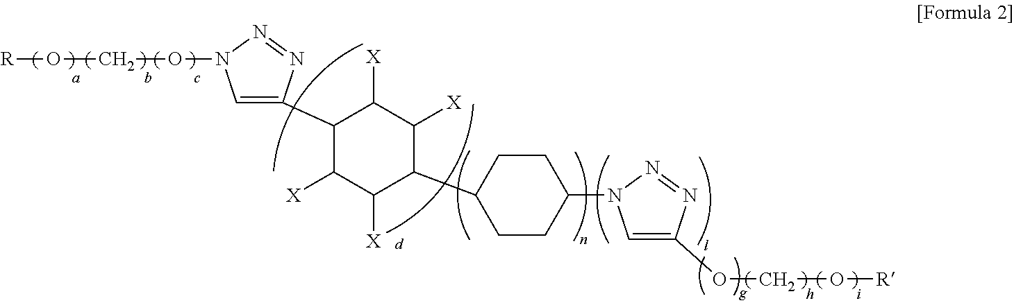


R5—B—VA [Formula 4]


R5—B—VA [Formula 4]


Claims (20)


R5—B—VA [Formula 4]


Applications Claiming Priority (2)
| Application Number | Priority Date | Filing Date | Title |
|---|---|---|---|
| KR1020150147508A KR20170047467A (en) | 2015-10-22 | 2015-10-22 | Liquid crystal compound and method for manufacturing liquid crystal display apparatus including the same |
| KR10-2015-0147508 | 2015-10-22 |
Publications (1)
| Publication Number | Publication Date |
|---|---|
| US9568774B1 true US9568774B1 (en) | 2017-02-14 |
Family
ID=57964451
Family Applications (1)
| Application Number | Title | Priority Date | Filing Date |
|---|---|---|---|
| US15/146,334 Active US9568774B1 (en) | 2015-10-22 | 2016-05-04 | Liquid crystal composition and method for manufacturing liquid crystal display apparatus including the same |
Country Status (2)
| Country | Link |
|---|---|
| US (1) | US9568774B1 (en) |
| KR (1) | KR20170047467A (en) |
Citations (2)
| Publication number | Priority date | Publication date | Assignee | Title |
|---|---|---|---|---|
| US20140240653A1 (en) | 2009-09-08 | 2014-08-28 | Merck Patent Gmbh | Liquid-crystal display |
| KR101540139B1 (en) | 2008-01-11 | 2015-07-28 | 메르크 파텐트 게엠베하 | Reactive mesogenic compounds and mixtures |
-
2015
- 2015-10-22 KR KR1020150147508A patent/KR20170047467A/en not_active Withdrawn
-
2016
- 2016-05-04 US US15/146,334 patent/US9568774B1/en active Active
Patent Citations (2)
| Publication number | Priority date | Publication date | Assignee | Title |
|---|---|---|---|---|
| KR101540139B1 (en) | 2008-01-11 | 2015-07-28 | 메르크 파텐트 게엠베하 | Reactive mesogenic compounds and mixtures |
| US20140240653A1 (en) | 2009-09-08 | 2014-08-28 | Merck Patent Gmbh | Liquid-crystal display |
Also Published As
| Publication number | Publication date |
|---|---|
| KR20170047467A (en) | 2017-05-08 |
Similar Documents
| Publication | Publication Date | Title |
|---|---|---|
| US8318270B2 (en) | Liquid crystal display panel and method of manufacturing the liquid crystal display panel | |
| US8623474B2 (en) | Liquid crystal display and method of manufacturing the same | |
| US9139777B2 (en) | Composition of liquid crystal medium | |
| CN103748507B (en) | The manufacture method of liquid crystal indicator | |
| TWI521283B (en) | Liquid crystal display panel and liquid crystal display device | |
| US20130287970A1 (en) | Liquid Crystal Medium Composition and Liquid Crystal Display Using Same | |
| US20100304015A1 (en) | Method for manufacturing a liquid crystal display panel and liquid crystal display panel | |
| US10824018B2 (en) | Thermal crosslink material, manufacture method of liquid crystal display panel and liquid crystal display panel | |
| US10018875B2 (en) | Curved liquid crystal display and method of manufacturing the same | |
| US20160032190A1 (en) | Composition for aligning, display panel and method of manufacturing same | |
| US9120971B2 (en) | Polymerizable mixture and liquid crystal composition thereof | |
| JP5113869B2 (en) | Liquid crystal display device and manufacturing method thereof | |
| US10527890B2 (en) | Liquid crystal display and manufacturing method thereof | |
| TW201314323A (en) | Liquid-crystal display panel and liquid-crystal display device | |
| US8218114B2 (en) | Liquid crystal display and method of manufacturing the same | |
| US10088709B2 (en) | Alignment layer composition, liquid crystal display including the same, and method of manufacturing the liquid crystal display | |
| WO2017084147A1 (en) | Reaction-type vertical alignment organosilicon material and method for manufacturing liquid crystal display panel | |
| US20160209707A1 (en) | Liquid crystal display and manufacturing method of making the liquid crystal display | |
| US9904113B2 (en) | Alignment composition, liquid crystal display panel and method of manufacturing same | |
| US9977288B2 (en) | Liquid crystal display | |
| US9568774B1 (en) | Liquid crystal composition and method for manufacturing liquid crystal display apparatus including the same | |
| US9733524B2 (en) | Liquid crystal display device and manufacturing method therefor | |
| US20190204648A1 (en) | Display panel, preparation method thereof, and liquid crystal display | |
| US10907101B2 (en) | Liquid crystal cell and liquid crystal display | |
| US20140293204A1 (en) | Liquid crystal composition and liquid crystal display panel thereof |
Legal Events
| Date | Code | Title | Description |
|---|---|---|---|
| AS | Assignment |
Owner name: SAMSUNG DISPLAY CO., LTD., KOREA, REPUBLIC OF Free format text: ASSIGNMENT OF ASSIGNORS INTEREST;ASSIGNORS:LIM, HO;AHN, HYUNKU;YANG, GIHOON;AND OTHERS;REEL/FRAME:038847/0903 Effective date: 20160419 |
|
| FEPP | Fee payment procedure |
Free format text: PAYOR NUMBER ASSIGNED (ORIGINAL EVENT CODE: ASPN); ENTITY STATUS OF PATENT OWNER: LARGE ENTITY |
|
| STCF | Information on status: patent grant |
Free format text: PATENTED CASE |
|
| MAFP | Maintenance fee payment |
Free format text: PAYMENT OF MAINTENANCE FEE, 4TH YEAR, LARGE ENTITY (ORIGINAL EVENT CODE: M1551); ENTITY STATUS OF PATENT OWNER: LARGE ENTITY Year of fee payment: 4 |
|
| MAFP | Maintenance fee payment |
Free format text: PAYMENT OF MAINTENANCE FEE, 8TH YEAR, LARGE ENTITY (ORIGINAL EVENT CODE: M1552); ENTITY STATUS OF PATENT OWNER: LARGE ENTITY Year of fee payment: 8 |