US9557381B1 - Physically aware insertion of diagnostic circuit elements - Google Patents
Physically aware insertion of diagnostic circuit elements Download PDFInfo
- Publication number
- US9557381B1 US9557381B1 US14/987,824 US201614987824A US9557381B1 US 9557381 B1 US9557381 B1 US 9557381B1 US 201614987824 A US201614987824 A US 201614987824A US 9557381 B1 US9557381 B1 US 9557381B1
- Authority
- US
- United States
- Prior art keywords
- segment
- processor
- adjacent
- objective function
- super
- Prior art date
- Legal status (The legal status is an assumption and is not a legal conclusion. Google has not performed a legal analysis and makes no representation as to the accuracy of the status listed.)
- Expired - Fee Related
Links
Images


Classifications
-
- G—PHYSICS
- G06—COMPUTING OR CALCULATING; COUNTING
- G06F—ELECTRIC DIGITAL DATA PROCESSING
- G06F30/00—Computer-aided design [CAD]
- G06F30/30—Circuit design
- G06F30/39—Circuit design at the physical level
- G06F30/392—Floor-planning or layout, e.g. partitioning or placement
-
- G—PHYSICS
- G01—MEASURING; TESTING
- G01R—MEASURING ELECTRIC VARIABLES; MEASURING MAGNETIC VARIABLES
- G01R31/00—Arrangements for testing electric properties; Arrangements for locating electric faults; Arrangements for electrical testing characterised by what is being tested not provided for elsewhere
- G01R31/28—Testing of electronic circuits, e.g. by signal tracer
- G01R31/317—Testing of digital circuits
- G01R31/3177—Testing of logic operation, e.g. by logic analysers
-
- G—PHYSICS
- G01—MEASURING; TESTING
- G01R—MEASURING ELECTRIC VARIABLES; MEASURING MAGNETIC VARIABLES
- G01R31/00—Arrangements for testing electric properties; Arrangements for locating electric faults; Arrangements for electrical testing characterised by what is being tested not provided for elsewhere
- G01R31/28—Testing of electronic circuits, e.g. by signal tracer
- G01R31/317—Testing of digital circuits
- G01R31/3181—Functional testing
- G01R31/3185—Reconfiguring for testing, e.g. LSSD, partitioning
- G01R31/318533—Reconfiguring for testing, e.g. LSSD, partitioning using scanning techniques, e.g. LSSD, Boundary Scan, JTAG
- G01R31/318541—Scan latches or cell details
-
- G—PHYSICS
- G01—MEASURING; TESTING
- G01R—MEASURING ELECTRIC VARIABLES; MEASURING MAGNETIC VARIABLES
- G01R31/00—Arrangements for testing electric properties; Arrangements for locating electric faults; Arrangements for electrical testing characterised by what is being tested not provided for elsewhere
- G01R31/28—Testing of electronic circuits, e.g. by signal tracer
- G01R31/317—Testing of digital circuits
- G01R31/3181—Functional testing
- G01R31/3183—Generation of test inputs, e.g. test vectors, patterns or sequences
- G01R31/318335—Test pattern compression or decompression
-
- G—PHYSICS
- G01—MEASURING; TESTING
- G01R—MEASURING ELECTRIC VARIABLES; MEASURING MAGNETIC VARIABLES
- G01R31/00—Arrangements for testing electric properties; Arrangements for locating electric faults; Arrangements for electrical testing characterised by what is being tested not provided for elsewhere
- G01R31/28—Testing of electronic circuits, e.g. by signal tracer
- G01R31/317—Testing of digital circuits
- G01R31/3181—Functional testing
- G01R31/3185—Reconfiguring for testing, e.g. LSSD, partitioning
- G01R31/318533—Reconfiguring for testing, e.g. LSSD, partitioning using scanning techniques, e.g. LSSD, Boundary Scan, JTAG
- G01R31/318536—Scan chain arrangements, e.g. connections, test bus, analog signals
-
- G—PHYSICS
- G06—COMPUTING OR CALCULATING; COUNTING
- G06F—ELECTRIC DIGITAL DATA PROCESSING
- G06F30/00—Computer-aided design [CAD]
- G06F30/30—Circuit design
-
- G—PHYSICS
- G01—MEASURING; TESTING
- G01R—MEASURING ELECTRIC VARIABLES; MEASURING MAGNETIC VARIABLES
- G01R31/00—Arrangements for testing electric properties; Arrangements for locating electric faults; Arrangements for electrical testing characterised by what is being tested not provided for elsewhere
- G01R31/28—Testing of electronic circuits, e.g. by signal tracer
- G01R31/317—Testing of digital circuits
- G01R31/3181—Functional testing
- G01R31/3185—Reconfiguring for testing, e.g. LSSD, partitioning
- G01R31/318533—Reconfiguring for testing, e.g. LSSD, partitioning using scanning techniques, e.g. LSSD, Boundary Scan, JTAG
- G01R31/318558—Addressing or selecting of subparts of the device under test
- G01R31/318563—Multiple simultaneous testing of subparts
-
- G—PHYSICS
- G01—MEASURING; TESTING
- G01R—MEASURING ELECTRIC VARIABLES; MEASURING MAGNETIC VARIABLES
- G01R31/00—Arrangements for testing electric properties; Arrangements for locating electric faults; Arrangements for electrical testing characterised by what is being tested not provided for elsewhere
- G01R31/28—Testing of electronic circuits, e.g. by signal tracer
- G01R31/317—Testing of digital circuits
- G01R31/3181—Functional testing
- G01R31/3185—Reconfiguring for testing, e.g. LSSD, partitioning
- G01R31/318533—Reconfiguring for testing, e.g. LSSD, partitioning using scanning techniques, e.g. LSSD, Boundary Scan, JTAG
- G01R31/318572—Input/Output interfaces
Definitions
- the present disclosure relates to diagnostic circuit elements, and more specifically, to physically aware insertion of diagnostic circuit elements.
- circuit elements for the purposes of diagnosing chip failures (such as XOR's in scan chains) were inserted with no consideration of physical layout properties.
- the result was poor spatial resolution for failure analysis, which made root cause defect identification difficult and time consuming due to large inspection areas.
- FIG. 1 a graph of area insertion mean segment length and area is shown, according to conventional methods.
- the area insertion mean is depicted as a function of XOR frequency.
- the size of the circle depicted in FIG. 1 represents how compact the circuits are in the layout.
- the large circle 1102 in the plot represents actual insertion properties for a 22 nm microprocessor product.
- the small circle 11 identifies an average logical resolution (y-axis) of ⁇ 20 circuits while the diameter of large circle 1102 is proportional to the average spatial resolution of chip circuit elements.
- the logical resolution is the average number of devices that a diagnostic element can identify. For example, as shown in the graph of FIG. 1 , for every one element inserted, about twenty normal circuits are identified. While a logical resolution of 20 circuit elements may be acceptable, the spatial resolution can make circuit analysis labor intense, time consuming, and costly.
- diagnostic elements into scan chains can affect a great number of things, including chip failure analysis, circuit power analysis and management, and extrapolation of relevant scan chain diagnosis information from a limited circuit sample.
- Current diagnostic methods may include blind placement or singular-ruled placement of diagnostic circuit elements, and may not provide a clear metric having a broad set of rules that may be applicable when determining where diagnostic circuit elements should be placed.
- a computer-implemented method for inserting diagnostic circuit elements in a scan chain of a chip may include creating, via a processor, a segment for each latch of a plurality of latches in the scan chain to create a plurality of adjacent and connected segments, merging, via the processor, the two adjacent and connected segments to form a super-segment comprising all latches contained in the two adjacent and connected segments based on the objective function, and inserting, via the processor, a logic circuit element between the super-segment and a segment that is adjacent and connected to the super-segment in the scan chain, where the logic circuit element allows diagnostic isolation of the scan chain super-segment.
- a system for inserting diagnostic circuit elements in a scan chain of a chip may include a processor configured to create a segment for each latch of a plurality of latches in the scan chain to create a plurality of adjacent and connected segments, merge the two adjacent and connected segments to form a super-segment comprising all latches contained in the two adjacent and connected segments, and insert a logic circuit element between the super-segment and a segment that is adjacent and connected to the super-segment in the scan chain, where the logic circuit element allows diagnostic isolation of a scan chain super-segment.
- a non-transitory computer-readable storage medium may include program instructions that are executable by a processor to perform a method for inserting diagnostic circuit elements in a scan chain of a chip.
- the method may include creating, via a processor, a segment for each latch of a plurality of latches in the scan chain to create a plurality of adjacent and connected segments, merging, via the processor, the two adjacent and connected segments to form a super-segment comprising all latches contained in the two adjacent and connected segments based on the objective function, and inserting, via the processor, a logic circuit element between the super-segment and a segment that is adjacent and connected to the super-segment in the scan chain, where the logic circuit element allows diagnostic isolation of the scan chain super-segment.
- FIG. 1 is a graph of area insertion mean segment length and area as a function of XOR frequency, according to known methods
- FIG. 2 illustrates a block diagram of a computer system for use in practicing the teachings herein;
- FIG. 3 depicts a block diagram of a scan chain in accordance with an exemplary embodiment
- FIG. 4 depicts a block diagram of physically aware insertion of diagnostic circuit elements in the scan chain of FIG. 3 in accordance with an exemplary embodiment
- FIG. 5 depicts a block diagram of physically aware insertion of diagnostic circuit elements of the scan chain of FIG. 3 in accordance with an exemplary embodiment
- FIG. 6 depicts a block diagram of physically aware insertion of diagnostic circuit elements the scan chain of FIG. 3 in accordance with an exemplary embodiment
- FIG. 7 depicts a flow diagram of an algorithm for physically aware sequential insertion of diagnostic circuit elements in accordance with an exemplary embodiment
- FIG. 8 depicts a flow diagram of an algorithm for sequentially inserting diagnostic circuit elements on a scan chain of a chip in accordance with an exemplary embodiment
- FIG. 9 depicts a flow diagram of a computer-implemented method for inserting diagnostic circuit elements on a scan chain of a chip in accordance with an exemplary embodiment
- FIG. 10 depicts a flow diagram for a computer-implemented method for creating an optimized objective function in accordance with an exemplary embodiment
- FIG. 11 is a graph of area insertion mean segment length and area as a function of XOR frequency, according to some embodiments.
- FIG. 2 illustrates a block diagram of a computer system 100 (hereafter “computer 100 ”) for use in practicing the embodiments described herein.
- the methods described herein can be implemented in hardware, software (e.g., firmware), or a combination thereof.
- the methods described herein are implemented in hardware, and may be part of the microprocessor of a special or general-purpose digital computer, such as a personal computer, workstation, minicomputer, or mainframe computer.
- Computer 100 therefore can embody a general-purpose computer.
- the methods described herein are implemented as part of a mobile device, such as, for example, a mobile phone, a personal data assistant (PDA), a tablet computer, etc.
- PDA personal data assistant
- the computer 100 includes processor 101 .
- Computer 100 also includes memory 102 coupled to processor 101 , and one or more input/output adaptors 103 , that may be communicatively coupled via system bus 105 .
- Memory 102 may be operatively coupled to one or more internal or external memory devices.
- Communications adaptor 104 may be operatively connect computer 100 to one or more networks 115 .
- a system bus 105 may also connect one or more user interfaces via interface adaptor 112 .
- Interface adaptor 112 may connect a plurality of user interfaces to computer 100 including, for example, keyboard 109 , mouse 110 , speaker 113 , etc.
- System bus 105 may also connect display adaptor 116 and display 117 to processor 101 .
- Processor 101 may also be operatively connected to graphical processing unit 118 .
- Processor 101 is a hardware device for executing hardware instructions or software, particularly that stored in a non-transitory computer-readable memory (e.g., memory 102 ).
- Processor 101 can be any custom made or commercially available processor, a central processing unit (CPU), a plurality of CPUs, for example, CPU 101 a - 101 c , an auxiliary processor among several other processors associated with the computer 100 , a semiconductor based microprocessor (in the form of a microchip or chip set), or generally any device for executing instructions.
- Processor 101 can include a memory cache 106 , which may include, but is not limited to, an instruction cache to speed up executable instruction fetch, a data cache to speed up data fetch and store, and a translation lookaside buffer (TLB) used to speed up virtual-to-physical address translation for both executable instructions and data.
- Cache 106 may be organized as a hierarchy of more cache levels (L1, L2, etc.).
- Memory 102 can include random access memory (RAM) 107 and read only memory (ROM) 108 .
- RAM 107 can be any one or combination of volatile memory elements (e.g., DRAM, SRAM, SDRAM, etc.).
- ROM 108 can include any one or more nonvolatile memory elements (e.g., erasable programmable read only memory (EPROM), flash memory, electronically erasable programmable read only memory (EEPROM), programmable read only memory (PROM), tape, compact disc read only memory (CD-ROM), disk, cartridge, cassette or the like, etc.).
- EPROM erasable programmable read only memory
- EEPROM electronically erasable programmable read only memory
- PROM programmable read only memory
- tape compact disc read only memory
- CD-ROM compact disc read only memory
- disk cartridge, cassette or the like, etc.
- memory 102 may incorporate electronic, magnetic, optical, and/or other types of non-transitory computer-readable storage media. Note that the memory 102 can
- the instructions in memory 102 may include one or more separate programs, each of which comprises an ordered listing of computer-executable instructions for implementing logical functions.
- the instructions in memory 102 may include an operating system 111 .
- Operating system 111 can control the execution of other computer programs and provides scheduling, input-output control, file and data management, memory management, and communication control and related services.
- Input/output adaptor 103 can be, for example but not limited to, one or more buses or other wired or wireless connections, as is known in the art. Input/output adaptor 103 may have additional elements, which are omitted for simplicity, such as controllers, buffers (caches), drivers, repeaters, and receivers, to enable communications. Further, the local interface may include address, control, and/or data connections to enable appropriate communications among the aforementioned components.
- Interface adaptor 112 may be configured to operatively connect one or more input/output (I/O) devices to computer 100 .
- interface adaptor 112 may connect a keyboard 109 and mouse 110 .
- Other output devices e.g., speaker 113 may be operatively connected to interface adaptor 112 .
- Other output devices may also be included, although not shown.
- devices may include but are not limited to a printer, a scanner, microphone, and/or the like.
- the I/O devices connectable to interface adaptor 112 may further include devices that communicate both inputs and outputs, for instance but not limited to, a network interface card (NIC) or modulator/demodulator (for accessing other files, devices, systems, or a network), a radio frequency (RF) or other transceiver, a telephonic interface, a bridge, a router, and the like.
- NIC network interface card
- RF radio frequency
- Computer 100 can further include display adaptor 116 coupled to one or more displays 117 .
- computer 100 can further include communications adaptor 104 for coupling to a network 115 .
- Network 115 can be an IP-based network for communication between computer 100 and any external device. Network 115 transmits and receives data between computer 100 and devices and/or systems external to computer 100 .
- network 115 can be a managed IP network administered by a service provider.
- Network 115 may be a network internal to an aircraft, such as, for example, an avionics network, etc.
- Network 115 may be implemented in a wireless fashion, e.g., using wireless protocols and technologies, such as WiFi, WiMax, etc.
- Network 115 may also be a wired network, e.g., an Ethernet network, an ARINC 429 network, a CAN, etc., having any wired connectivity including, e.g., an RS232 connection, R5422 connection, etc.
- Network 115 can also be a packet-switched network such as a local area network, wide area network, metropolitan area network, Internet network, or other similar type of network environment.
- the network 115 may be a fixed wireless network, a wireless local area network (LAN), a wireless wide area network (WAN) a personal area network (PAN), a virtual private network (VPN), intranet or other suitable network system.
- LAN wireless local area network
- WAN wireless wide area network
- PAN personal area network
- VPN virtual private network
- the instructions in the memory 102 may further include a basic input output system (BIOS) (omitted for simplicity).
- BIOS is a set of essential routines that initialize and test hardware at startup, start operating system 111 , and support the transfer of data among the operatively connected hardware devices.
- the BIOS is stored in ROM 108 so that the BIOS can be executed when computer 100 is activated.
- processor 101 may be configured to execute instructions stored within the memory 102 , to communicate data to and from the memory 102 , and to generally control operations of the computer 100 pursuant to the instructions.
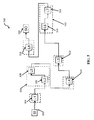
- FIG. 3 depicts a block diagram of a scan chain, in accordance with an exemplary embodiment.
- exemplary scan chain 300 is depicted.
- Scan chain 300 is shown with a scan input pin 302 , a scan output pin 320 , and a plurality of latches 304 - 318 .
- Each of latches 304 - 318 may be connected to an adjacent latch by a connecting wire 305 .
- the shape of scan chain 300 is arbitrarily non-linear to represent an example shape of a scan chain on a physical chip, as implemented in practice. In most instances, the scan chain can span very small distances between latches to relatively long distances that span most of or all of the width of the physical chip.
- the shape of scan chain 300 and the number of latches 304 - 318 are arbitrary and may be configured with any number of shapes and latches.
- Circuit elements e.g., MUXs, and-or-invert (AOI) circuits, XORs, etc.
- AOI AOI-invert
- scan chain 300 may include up to 20 latches (although 8 are shown in FIG. 3 for simplicity).
- Current diagnostic methods may include blind placement or singular-ruled placement of diagnostic circuit elements. In some instances, current methods may not provide a clear metric having a broad set of rules that may be applicable when determining where diagnostic circuit elements should be placed.
- each latch in scan chain 300 would have a logic circuit separating it from each successive latch. Accordingly, if one latch or connecting wire (e.g., connecting wire 305 separating virtual segments/latches L 1 303 and L 2 306 ) contained a defect, the intervening logic circuit (not shown) could identify the exact location of the defect.
- latch L 1 304 would ideally be segmented into its own virtual segment 303 .
- Scan chain 300 is depicted with the latches having virtual segments of a single latch, as illustrated by the dashed lines surrounding each of latches 304 - 318 .
- FIG. 4 depicts a block diagram of physically aware insertion of diagnostic circuit elements in scan chain 300 , in accordance with an exemplary embodiment.
- the primary function of some embodiments may be to reduce a total segment (thereby reducing the area for a PFA to analyze in connection with a logic error)
- another objective may be grouping together particular latch design types (e.g., it may be advantageous to cluster nlats vs slats vs. eslats).
- an objective function may include grouping together timing elements (thereby clustering circuit elements with a predetermined timing).
- an objective function may include grouping latches having a maximum or minimum connecting wire length between latches.
- an objective function may be based on a total iteration count (e.g., processor 101 may stop after a predetermined number of iterations). In other aspects, an objective function may be based on a cell count. Other embodiments may include grouping scan chain elements according to the connectivity to specific elements (e.g., grouping elements connected to particular LCB clusters), etc. Regardless of the particular objective function, processor 101 may meet an objective function, by intelligently grouping together scan chain segments and placing physical (real) circuit elements between the optimized super-segments.
- processor 101 may create a virtual segment for each latch of a plurality of latches in the scan chain to create a plurality of adjacent and connected segments.
- processor 101 may group together adjacent latches to form one or more super-segments meeting an objective of having minimal combined bounding area (which would optimize the area for each segment separated by diagnostic circuit element that allows diagnostic isolation of the scan chain super-segment).
- processor 101 may place a virtual diagnostic circuit element (e.g., virtual segment 303 ) between two adjacent latches. With a virtual diagnostic circuit element between each of the latches (the ideal scenario), processor 101 may work backward to analyze the entire scan chain 300 and find the optimal configuration for grouping each of the virtual segments into actual super-segments.
- processor 101 may analyze all of latches 304 - 318 and determine at least two latches (e.g., latches L 2 306 and L 3 308 ) that may satisfy the objective of minimizing the combined bounding area. For example, processor 101 may examine the relative distances between each of latches 304 - 320 and calculate a distance between all segments (L 1 to L 2 , L 2 to L 3 , etc.). If the objective function is to minimize bounding area, processor 101 may determine that the smallest distances between elements exists between latches L 2 306 and L 3 308 .
- Processor 101 may next remove a (virtual) diagnostic element intervening latches L 2 306 and L 3 308 , and combine latch L 2 306 and latch L 3 308 to form a 2-latch super-segment 402 .
- a (virtual) diagnostic element intervening latches L 2 306 and L 3 308 , and combine latch L 2 306 and latch L 3 308 to form a 2-latch super-segment 402 .
- any segment made to include two or more latches can be referred to as a super-segment.
- processor 101 may remove a virtual diagnostic circuit element separating latch L 2 306 and latch L 3 308 based on a determination that this latch group (in this case, a pair of latches) may have the smallest possible area left over once the intervening (virtual) diagnostic circuit element is removed, and a super-segment 402 is formed.
- Processor 101 may next cycle through each of the remaining latches in scan chain 300 to group together other groups of latches that best meet the objective function of minimizing bounding area. Referring now to FIG. 5 , processor 101 may determine that another group of latches L 6 314 and L 7 316 satisfy the objective function, remove an intervening virtual diagnostic circuit element (not shown), and form super-segment 502 .
- processor 101 may determine that an optimal super-segment 604 should now include latch L 1 304 , and may group latches L 4 310 and L 5 312 to form super-segment 606 . Accordingly, processor 101 may repeat identifying and merging until a predetermined rule is satisfied. Stated in other terms, processor may stop when the creation of another super-segment in a scan chain breaks a predetermined rule established for the particular objective function.
- a predetermined rule may state that a super segment may not exceed an area of 150 microns. If the addition of any segments or super-segments to super-segment 606 breaks the predetermined rule, then processor 101 may analyze the remaining segments and super-segments until it has determined that any more merges would break the predetermined rule. Once processor 101 terminates the merging process, processor 101 may insert one or more logic circuit elements 608 (e.g., XORs) between each remaining virtual segment block to create actual segments on the physical chip. Insertion of logic circuit elements 608 may allow diagnostic isolation of the scan chain segments.
- logic circuit elements 608 e.g., XORs
- processor 101 can instantiate a priority queue to keep adjacent segment pairs ordered by combined area for logarithmic time (e.g., O(log n)) operations.
- the largest cost may likely be the O(n) time required to build the initial heap.
- processor 101 may create a segment 303 for each latch 304 - 318 in chain 300 .
- processor 101 may find the two adjacent connected segments having a minimal combined bounding area, as shown in block 704 .
- processor may determine whether new bounds of a theoretically combined super-segment (e.g., super-segment 402 ) are less than or equal to a predetermined rule for area constraints.
- processor 101 may merge the segments into a new segment, as shown in block 708 . If processor 101 determines at decision block 706 that the new bounds area is not less than or equal to the area constraint, then processor 101 may omit the merge step of block 708 and directly insert a logic device between segments, as shown in block 712 . Accordingly, processor 101 may iterate through each of the remaining segments and/or super-segments until, as seen in block 710 , processor 101 determines that there are no more additional segments in the scan chain to analyze.
- FIG. 8 depicts a flow diagram of an algorithm 800 for sequentially inserting diagnostic circuit elements on a scan chain of a chip, in accordance with an exemplary embodiment.
- processor 101 may discover the chain from the input pin automatically.
- processor 101 may discover the chain based on a predetermined rule. For example, processor 101 may use an objective function as described above, and determine whether a predetermined rule associated with the objective is violated.
- processor 101 may start at a first latch (e.g., starting latch SI 302 shown with respect to FIG. 3 ), and create a segment for a first latch L 1 304 .
- processor 101 may start a new segment with the next latch, and add the next adjacent connected latch to the segment (as shown in block 808 ) if processor determines at decision block 806 that there is another sequential latch available in the scan chain.
- processor 101 may determine whether the predetermined rule is violated (e.g., whether the new theoretical area bounds are less than the predetermined constraint area).
- processor 101 may insert a logic device before the last latch added to the segment if the constraint is not violated.
- processor 101 may determine if there are any remaining latches, and iteratively continue until the end latch of the scan chain is reached.
- FIG. 9 depicts a flow diagram of a computer-implemented method 900 for inserting diagnostic circuit elements on a scan chain of a chip, in accordance with an exemplary embodiment.
- processor 101 may create a segment for each latch of a plurality of latches 304 - 318 in a scan chain 300 to create a plurality of adjacent and connected segments.
- processor 101 may identify two adjacent and connected segments that satisfy an objective function (e.g., super-segment 402 ).
- Processor 101 may then merge the two adjacent and connected segments/latches (e.g., latch L 1 304 and latch L 2 308 ) to form a super-segment 402 that may include all latches contained in the two adjacent and connected segments latch L 1 305 and latch L 2 308 .
- Processor 101 can repeat the steps described with respect to blocks 904 and 906 until a predetermined rule would be broken with the next merge.
- processor 101 may insert a logic circuit 608 between the super-segment in scan chain 300 where the logic circuit 608 allows diagnostic isolation of a scan chain super-segment (e.g., isolation of super-segments 604 , 606 , 502 , segment 318 , etc.).
- FIG. 10 depicts a method 1000 for creating an optimized objective function, in accordance with an exemplary embodiment.
- processor 101 may select one or more parameters associated with the objective function.
- processor 101 may determine a weighted value for each of the one or more parameters selected, and define an aggregate threshold value, as shown in block 1006 .
- the aggregated threshold value may be a value that should not be exceeded by the sum of weighted parameter values. For example, if more than one parameter value is selected by a user, processor 101 may request user input regarding weighted values with respect to each of the selected parameters.
- processor 101 may attribute a weighted value to each selected parameter based on the user input, add up an aggregated score of the weighted values, as shown in block 1008 , and determine if the sum exceeds the aggregate threshold value (as shown in block 1010 ). Accordingly, processor 101 may assign a heavier weight with respective objectives, and group scan chain elements accordingly.
- weights for each parameter could be specified by a user based on the extent to which they cared about a parameter (eg. 80% area, 20% latch count, etc., if the user cared strongly about meeting the area objective).
- FIG. 11 a graph of area insertion mean segment length and area as a function of XOR frequency is depicted, according to some embodiments.
- the graph shows potential physical resolution opportunities when diagnostic circuits are placed with spatial awareness.
- the large circle 1102 in the plot represents actual insertion properties for a 22 nm server product.
- the solid inner circles represent exemplary resolutions 1104 , 1106 , 1108 , 1110 , 1112 , 1114 and 1116 , which may be average spatial resolutions for particular segment lengths, while the outer “halo” circles depicted in dashed lines surrounding each of resolutions 1104 - 1116 represent spatial resolution maximums for each respective inner circle.
- the logical resolution is the average number of devices that a logical element can identify.
- resolution 1116 shows a square area of 40 ⁇ 40 microns
- resolution 1114 depicts 50 ⁇ 50
- resolution 1110 shown 75 ⁇ 75 microns
- resolution 1108 depicts 100 ⁇ 100 microns
- resolution 1106 depicts 150 ⁇ 150 microns
- resolution 1104 depicts 200 ⁇ 200 microns.
- some physically aware optimization algorithms can reach roughly the same logical resolution while vastly reducing average and maximum spatial resolution using fewer insertions (x-axis). The dramatic reduction in care area can result in improved diagnostic localization, faster circuit analysis turn-around, reduced expense, and improved yield learning rates.
- the present invention may be a system, a method, and/or a computer program product at any possible technical detail level of integration
- the computer program product may include a computer readable storage medium (or media) having computer readable program instructions thereon for causing a processor to carry out aspects of the present invention
- the computer readable storage medium can be a tangible device that can retain and store instructions for use by an instruction execution device.
- the computer readable storage medium may be, for example, but is not limited to, an electronic storage device, a magnetic storage device, an optical storage device, an electromagnetic storage device, a semiconductor storage device, or any suitable combination of the foregoing.
- a non-exhaustive list of more specific examples of the computer readable storage medium includes the following: a portable computer diskette, a hard disk, a random access memory (RAM), a read-only memory (ROM), an erasable programmable read-only memory (EPROM or Flash memory), a static random access memory (SRAM), a portable compact disc read-only memory (CD-ROM), a digital versatile disk (DVD), a memory stick, a floppy disk, a mechanically encoded device such as punch-cards or raised structures in a groove having instructions recorded thereon, and any suitable combination of the foregoing.
- RAM random access memory
- ROM read-only memory
- EPROM or Flash memory erasable programmable read-only memory
- SRAM static random access memory
- CD-ROM compact disc read-only memory
- DVD digital versatile disk
- memory stick a floppy disk
- a mechanically encoded device such as punch-cards or raised structures in a groove having instructions recorded thereon
- a computer readable storage medium is not to be construed as being transitory signals per se, such as radio waves or other freely propagating electromagnetic waves, electromagnetic waves propagating through a waveguide or other transmission media (e.g., light pulses passing through a fiber-optic cable), or electrical signals transmitted through a wire.
- Computer readable program instructions described herein can be downloaded to respective computing/processing devices from a computer readable storage medium or to an external computer or external storage device via a network, for example, the Internet, a local area network, a wide area network and/or a wireless network.
- the network may comprise copper transmission cables, optical transmission fibers, wireless transmission, routers, firewalls, switches, gateway computers and/or edge servers.
- a network adapter card or network interface in each computing/processing device receives computer readable program instructions from the network and forwards the computer readable program instructions for storage in a computer readable storage medium within the respective computing/processing device.
- Computer readable program instructions for carrying out operations of the present invention may be assembler instructions, instruction-set-architecture (ISA) instructions, machine instructions, machine dependent instructions, microcode, firmware instructions, state-setting data, configuration data for integrated circuitry, or either source code or object code written in any combination of one or more programming languages, including an object oriented programming language such as Smalltalk, C++, or the like, and procedural programming languages, such as the “C” programming language or similar programming languages.
- the computer readable program instructions may execute entirely on the user's computer, partly on the user's computer, as a stand-alone software package, partly on the user's computer and partly on a remote computer or entirely on the remote computer or server.
- the remote computer may be connected to the user's computer through any type of network, including a local area network (LAN) or a wide area network (WAN), or the connection may be made to an external computer (for example, through the Internet using an Internet Service Provider).
- electronic circuitry including, for example, programmable logic circuitry, field-programmable gate arrays (FPGA), or programmable logic arrays (PLA) may execute the computer readable program instructions IBM Confidential; Attorney Work Product; Attorney Client Privileged Aug. 24, 2015 D-2 by utilizing state information of the computer readable program instructions to personalize the electronic circuitry, in order to perform aspects of the present invention.
- These computer readable program instructions may be provided to a processor of a general purpose computer, special purpose computer, or other programmable data processing apparatus to produce a machine, such that the instructions, which execute via the processor of the computer or other programmable data processing apparatus, create means for implementing the functions/acts specified in the flowchart and/or block diagram block or blocks.
- These computer readable program instructions may also be stored in a computer readable storage medium that can direct a computer, a programmable data processing apparatus, and/or other devices to function in a particular manner, such that the computer readable storage medium having instructions stored therein comprises an article of manufacture including instructions which implement aspects of the function/act specified in the flowchart and/or block diagram block or blocks.
- the computer readable program instructions may also be loaded onto a computer, other programmable data processing apparatus, or other device to cause a series of operational steps to be performed on the computer, other programmable apparatus or other device to produce a computer implemented process, such that the instructions which execute on the computer, other programmable apparatus, or other device implement the functions/acts specified in the flowchart and/or block diagram block or blocks.
- each block in the flowchart or block diagrams may represent a module, segment, or portion of instructions, which comprises one or more executable instructions for implementing the specified logical function(s).
- the functions noted in the blocks may occur out of the order noted in the Figures.
- two blocks shown in succession may, in fact, be executed substantially concurrently, or the blocks may sometimes be executed in the reverse order, depending upon the functionality involved.
Landscapes
- Engineering & Computer Science (AREA)
- Physics & Mathematics (AREA)
- General Engineering & Computer Science (AREA)
- General Physics & Mathematics (AREA)
- Computer Hardware Design (AREA)
- Theoretical Computer Science (AREA)
- Evolutionary Computation (AREA)
- Geometry (AREA)
- Architecture (AREA)
- Tests Of Electronic Circuits (AREA)
Abstract
Description
Claims (18)
Priority Applications (1)
| Application Number | Priority Date | Filing Date | Title |
|---|---|---|---|
| US14/987,824 US9557381B1 (en) | 2016-01-05 | 2016-01-05 | Physically aware insertion of diagnostic circuit elements |
Applications Claiming Priority (1)
| Application Number | Priority Date | Filing Date | Title |
|---|---|---|---|
| US14/987,824 US9557381B1 (en) | 2016-01-05 | 2016-01-05 | Physically aware insertion of diagnostic circuit elements |
Publications (1)
| Publication Number | Publication Date |
|---|---|
| US9557381B1 true US9557381B1 (en) | 2017-01-31 |
Family
ID=57867284
Family Applications (1)
| Application Number | Title | Priority Date | Filing Date |
|---|---|---|---|
| US14/987,824 Expired - Fee Related US9557381B1 (en) | 2016-01-05 | 2016-01-05 | Physically aware insertion of diagnostic circuit elements |
Country Status (1)
| Country | Link |
|---|---|
| US (1) | US9557381B1 (en) |
Citations (26)
| Publication number | Priority date | Publication date | Assignee | Title |
|---|---|---|---|---|
| US5748497A (en) * | 1994-10-31 | 1998-05-05 | Texas Instruments Incorporated | System and method for improving fault coverage of an electric circuit |
| US5881067A (en) | 1997-01-28 | 1999-03-09 | Sun Microsystems, Inc. | Flip-flop design and technique for scan chain diagnosis |
| US6370664B1 (en) * | 1998-10-29 | 2002-04-09 | Agere Systems Guardian Corp. | Method and apparatus for partitioning long scan chains in scan based BIST architecture |
| US20030005363A1 (en) | 2001-06-29 | 2003-01-02 | Bassett Robert W. | Apparatus and method for hardware-assisted diagnosis of broken logic-test shift-registers |
| US6615380B1 (en) | 1999-12-21 | 2003-09-02 | Synopsys Inc. | Dynamic scan chains and test pattern generation methodologies therefor |
| US6681356B1 (en) | 2000-09-29 | 2004-01-20 | International Business Machines Corporation | Scan chain connectivity |
| US20050210349A1 (en) * | 2004-03-22 | 2005-09-22 | Lambert Michael R | Scan test tools, models and/or methods |
| US6986090B2 (en) | 2002-02-20 | 2006-01-10 | International Business Machines Corporation | Method for reducing switching activity during a scan operation with limited impact on the test coverage of an integrated circuit |
| US7139950B2 (en) | 2004-01-28 | 2006-11-21 | International Business Machines Corporation | Segmented scan chains with dynamic reconfigurations |
| US7181664B2 (en) | 2004-04-19 | 2007-02-20 | Chang Gung University | Method on scan chain reordering for lowering VLSI power consumption |
| US7188323B2 (en) | 2004-04-20 | 2007-03-06 | Nec Laboratories America, Inc. | Restricted scan reordering technique to enhance delay fault coverage |
| US7263641B2 (en) * | 1999-11-23 | 2007-08-28 | Janusz Rajski | Phase shifter with reduced linear dependency |
| US7376915B1 (en) | 2004-10-07 | 2008-05-20 | Cirrus Logic, Inc. | Methods for forming area-efficient scan chains in integrated circuits, and integrated circuits embodying the same |
| US7412636B2 (en) * | 2005-08-23 | 2008-08-12 | Oc Applications Research Llc | Scan string segmentation for digital test compression |
| US7461307B2 (en) * | 2005-05-06 | 2008-12-02 | Lsi Corporation | System and method for improving transition delay fault coverage in delay fault tests through use of an enhanced scan flip-flop |
| US20090288045A1 (en) | 2008-05-19 | 2009-11-19 | Synopsys, Inc. | Design-For-Test-Aware Hierarchical Design Planning |
| US7729884B2 (en) * | 2004-03-31 | 2010-06-01 | Yu Huang | Compactor independent direct diagnosis of test hardware |
| US7752515B2 (en) * | 2002-06-11 | 2010-07-06 | Dervisoglu Bulent I | Accelerated scan circuitry and method for reducing scan test data volume and execution time |
| US7900103B2 (en) | 2006-12-22 | 2011-03-01 | Stmicroelectronics S.R.L. | Scan chain architecture for increased diagnostic capability in digital electronic devices |
| US7954025B2 (en) | 2006-09-19 | 2011-05-31 | Marvell International Ltd. | Scan architecture for full custom blocks |
| US7958472B2 (en) | 2008-09-30 | 2011-06-07 | Synopsys, Inc. | Increasing scan compression by using X-chains |
| US7996805B2 (en) | 2008-01-08 | 2011-08-09 | National Semiconductor Corporation | Method of stitching scan flipflops together to form a scan chain with a reduced wire length |
| US7996800B2 (en) | 2005-02-03 | 2011-08-09 | International Business Machines Corporation | Computer program product for design verification using sequential and combinational transformations |
| US20120030532A1 (en) * | 2010-07-27 | 2012-02-02 | Texas Instruments Incorporated | Structures and control processes for efficient generation of different test clocking sequences, controls and other test signals in scan designs with multiple partitions, and devices, systems and processes of making |
| US8443326B1 (en) | 2012-04-10 | 2013-05-14 | Freescale Semiconductor, Inc. | Scan chain re-ordering in electronic circuit design based on region congestion in layout plan |
| US8782591B1 (en) | 2012-12-31 | 2014-07-15 | Cadence Design Systems, Inc. | Physically aware logic synthesis of integrated circuit designs |
-
2016
- 2016-01-05 US US14/987,824 patent/US9557381B1/en not_active Expired - Fee Related
Patent Citations (26)
| Publication number | Priority date | Publication date | Assignee | Title |
|---|---|---|---|---|
| US5748497A (en) * | 1994-10-31 | 1998-05-05 | Texas Instruments Incorporated | System and method for improving fault coverage of an electric circuit |
| US5881067A (en) | 1997-01-28 | 1999-03-09 | Sun Microsystems, Inc. | Flip-flop design and technique for scan chain diagnosis |
| US6370664B1 (en) * | 1998-10-29 | 2002-04-09 | Agere Systems Guardian Corp. | Method and apparatus for partitioning long scan chains in scan based BIST architecture |
| US7263641B2 (en) * | 1999-11-23 | 2007-08-28 | Janusz Rajski | Phase shifter with reduced linear dependency |
| US6615380B1 (en) | 1999-12-21 | 2003-09-02 | Synopsys Inc. | Dynamic scan chains and test pattern generation methodologies therefor |
| US6681356B1 (en) | 2000-09-29 | 2004-01-20 | International Business Machines Corporation | Scan chain connectivity |
| US20030005363A1 (en) | 2001-06-29 | 2003-01-02 | Bassett Robert W. | Apparatus and method for hardware-assisted diagnosis of broken logic-test shift-registers |
| US6986090B2 (en) | 2002-02-20 | 2006-01-10 | International Business Machines Corporation | Method for reducing switching activity during a scan operation with limited impact on the test coverage of an integrated circuit |
| US7752515B2 (en) * | 2002-06-11 | 2010-07-06 | Dervisoglu Bulent I | Accelerated scan circuitry and method for reducing scan test data volume and execution time |
| US7139950B2 (en) | 2004-01-28 | 2006-11-21 | International Business Machines Corporation | Segmented scan chains with dynamic reconfigurations |
| US20050210349A1 (en) * | 2004-03-22 | 2005-09-22 | Lambert Michael R | Scan test tools, models and/or methods |
| US7729884B2 (en) * | 2004-03-31 | 2010-06-01 | Yu Huang | Compactor independent direct diagnosis of test hardware |
| US7181664B2 (en) | 2004-04-19 | 2007-02-20 | Chang Gung University | Method on scan chain reordering for lowering VLSI power consumption |
| US7188323B2 (en) | 2004-04-20 | 2007-03-06 | Nec Laboratories America, Inc. | Restricted scan reordering technique to enhance delay fault coverage |
| US7376915B1 (en) | 2004-10-07 | 2008-05-20 | Cirrus Logic, Inc. | Methods for forming area-efficient scan chains in integrated circuits, and integrated circuits embodying the same |
| US7996800B2 (en) | 2005-02-03 | 2011-08-09 | International Business Machines Corporation | Computer program product for design verification using sequential and combinational transformations |
| US7461307B2 (en) * | 2005-05-06 | 2008-12-02 | Lsi Corporation | System and method for improving transition delay fault coverage in delay fault tests through use of an enhanced scan flip-flop |
| US7412636B2 (en) * | 2005-08-23 | 2008-08-12 | Oc Applications Research Llc | Scan string segmentation for digital test compression |
| US7954025B2 (en) | 2006-09-19 | 2011-05-31 | Marvell International Ltd. | Scan architecture for full custom blocks |
| US7900103B2 (en) | 2006-12-22 | 2011-03-01 | Stmicroelectronics S.R.L. | Scan chain architecture for increased diagnostic capability in digital electronic devices |
| US7996805B2 (en) | 2008-01-08 | 2011-08-09 | National Semiconductor Corporation | Method of stitching scan flipflops together to form a scan chain with a reduced wire length |
| US20090288045A1 (en) | 2008-05-19 | 2009-11-19 | Synopsys, Inc. | Design-For-Test-Aware Hierarchical Design Planning |
| US7958472B2 (en) | 2008-09-30 | 2011-06-07 | Synopsys, Inc. | Increasing scan compression by using X-chains |
| US20120030532A1 (en) * | 2010-07-27 | 2012-02-02 | Texas Instruments Incorporated | Structures and control processes for efficient generation of different test clocking sequences, controls and other test signals in scan designs with multiple partitions, and devices, systems and processes of making |
| US8443326B1 (en) | 2012-04-10 | 2013-05-14 | Freescale Semiconductor, Inc. | Scan chain re-ordering in electronic circuit design based on region congestion in layout plan |
| US8782591B1 (en) | 2012-12-31 | 2014-07-15 | Cadence Design Systems, Inc. | Physically aware logic synthesis of integrated circuit designs |
Similar Documents
| Publication | Publication Date | Title |
|---|---|---|
| US11086619B2 (en) | Code analytics and publication platform | |
| US9171167B2 (en) | Methods and systems for use in analyzing cyber-security threats in an aviation platform | |
| US10891178B2 (en) | Method and device for identifying problematic component in storage system | |
| US8949676B2 (en) | Real-time event storm detection in a cloud environment | |
| US8572574B2 (en) | Solving hybrid constraints to validate specification requirements of a software module | |
| EP2420931A1 (en) | Solving hybrid constraints to generate test cases for validating a software module | |
| US20120017200A1 (en) | Solving Hybrid Constraints to Validate a Security Software Module for Detecting Injection Attacks | |
| US10162326B2 (en) | Self-adjusting test time estimation | |
| US9772895B2 (en) | Identifying intervals of unusual activity in information technology systems | |
| CN105511957A (en) | Method and system for generating work alarm | |
| CN116028317A (en) | Method, electronic device and computer program product for training fault analysis model | |
| US11775654B2 (en) | Anomaly detection with impact assessment | |
| US11586491B2 (en) | Service issue source identification in an interconnected environment | |
| US11675009B2 (en) | Converting formal verification testbench drivers with nondeterministic inputs to simulation monitors | |
| US20210089299A1 (en) | Removing Feature Flag-Related Codebase from Applications | |
| CN112765101A (en) | Method, electronic device and computer program product for managing a file system | |
| US20180314516A1 (en) | Efficient software testing | |
| US9934327B2 (en) | Mining relevant approximate subgraphs from multigraphs | |
| US20200019652A1 (en) | Integrated circuit design model splitting for formal verification | |
| US20170192485A1 (en) | Providing a power optimized design for a device | |
| US20210294681A1 (en) | Incident root cause analysis using galois connections | |
| US9557381B1 (en) | Physically aware insertion of diagnostic circuit elements | |
| US11176010B2 (en) | Circuit-cycle reproduction | |
| US11429871B2 (en) | Detection of data offloading through instrumentation analysis | |
| US11243986B1 (en) | Method for proactive trouble-shooting of provisioning workflows for efficient cloud operations |
Legal Events
| Date | Code | Title | Description |
|---|---|---|---|
| AS | Assignment |
Owner name: INTERNATIONAL BUSINESS MACHINES CORPORATION, NEW Y Free format text: ASSIGNMENT OF ASSIGNORS INTEREST;ASSIGNORS:HUOTT, WILLIAM V.;KUSKO, MARY P.;RANGARAJAN, SRIDHAR H.;AND OTHERS;SIGNING DATES FROM 20151214 TO 20151216;REEL/FRAME:037411/0148 |
|
| STCF | Information on status: patent grant |
Free format text: PATENTED CASE |
|
| MAFP | Maintenance fee payment |
Free format text: PAYMENT OF MAINTENANCE FEE, 4TH YEAR, LARGE ENTITY (ORIGINAL EVENT CODE: M1551); ENTITY STATUS OF PATENT OWNER: LARGE ENTITY Year of fee payment: 4 |
|
| FEPP | Fee payment procedure |
Free format text: MAINTENANCE FEE REMINDER MAILED (ORIGINAL EVENT CODE: REM.); ENTITY STATUS OF PATENT OWNER: LARGE ENTITY |
|
| LAPS | Lapse for failure to pay maintenance fees |
Free format text: PATENT EXPIRED FOR FAILURE TO PAY MAINTENANCE FEES (ORIGINAL EVENT CODE: EXP.); ENTITY STATUS OF PATENT OWNER: LARGE ENTITY |
|
| STCH | Information on status: patent discontinuation |
Free format text: PATENT EXPIRED DUE TO NONPAYMENT OF MAINTENANCE FEES UNDER 37 CFR 1.362 |
|
| FP | Lapsed due to failure to pay maintenance fee |
Effective date: 20250131 |