US9548457B2 - Spirofluorene derivative, material for light-emitting element, light-emitting element, light-emitting device, and electronic device - Google Patents
Spirofluorene derivative, material for light-emitting element, light-emitting element, light-emitting device, and electronic device Download PDFInfo
- Publication number
- US9548457B2 US9548457B2 US14/950,613 US201514950613A US9548457B2 US 9548457 B2 US9548457 B2 US 9548457B2 US 201514950613 A US201514950613 A US 201514950613A US 9548457 B2 US9548457 B2 US 9548457B2
- Authority
- US
- United States
- Prior art keywords
- group
- light
- electrode
- carbon atoms
- layer
- Prior art date
- Legal status (The legal status is an assumption and is not a legal conclusion. Google has not performed a legal analysis and makes no representation as to the accuracy of the status listed.)
- Active
Links
- 239000000463 material Substances 0.000 title claims abstract description 131
- 239000000758 substrate Substances 0.000 claims description 74
- 239000004065 semiconductor Substances 0.000 claims description 49
- 239000011521 glass Substances 0.000 claims description 19
- 229910052581 Si3N4 Inorganic materials 0.000 claims description 12
- HQVNEWCFYHHQES-UHFFFAOYSA-N silicon nitride Chemical compound N12[Si]34N5[Si]62N3[Si]51N64 HQVNEWCFYHHQES-UHFFFAOYSA-N 0.000 claims description 12
- 239000011777 magnesium Substances 0.000 claims description 9
- 229910052709 silver Inorganic materials 0.000 claims description 8
- FYYHWMGAXLPEAU-UHFFFAOYSA-N Magnesium Chemical compound [Mg] FYYHWMGAXLPEAU-UHFFFAOYSA-N 0.000 claims description 7
- ZOKXTWBITQBERF-UHFFFAOYSA-N Molybdenum Chemical compound [Mo] ZOKXTWBITQBERF-UHFFFAOYSA-N 0.000 claims description 7
- 229910052749 magnesium Inorganic materials 0.000 claims description 7
- 229910052750 molybdenum Inorganic materials 0.000 claims description 7
- 239000011733 molybdenum Substances 0.000 claims description 7
- 239000004332 silver Substances 0.000 claims description 5
- 125000004432 carbon atom Chemical group C* 0.000 abstract description 175
- 125000000217 alkyl group Chemical group 0.000 abstract description 117
- 239000001257 hydrogen Substances 0.000 abstract description 105
- 229910052739 hydrogen Inorganic materials 0.000 abstract description 105
- 125000003118 aryl group Chemical group 0.000 abstract description 58
- UFHFLCQGNIYNRP-UHFFFAOYSA-N Hydrogen Chemical compound [H][H] UFHFLCQGNIYNRP-UHFFFAOYSA-N 0.000 abstract description 53
- 150000002431 hydrogen Chemical class 0.000 abstract description 49
- 239000010410 layer Substances 0.000 description 310
- 239000010408 film Substances 0.000 description 125
- VLKZOEOYAKHREP-UHFFFAOYSA-N n-Hexane Chemical compound CCCCCC VLKZOEOYAKHREP-UHFFFAOYSA-N 0.000 description 69
- 150000002894 organic compounds Chemical class 0.000 description 66
- 125000000999 tert-butyl group Chemical group [H]C([H])([H])C(*)(C([H])([H])[H])C([H])([H])[H] 0.000 description 65
- YXFVVABEGXRONW-UHFFFAOYSA-N Toluene Chemical compound CC1=CC=CC=C1 YXFVVABEGXRONW-UHFFFAOYSA-N 0.000 description 54
- ZUOUZKKEUPVFJK-UHFFFAOYSA-N diphenyl Chemical group C1=CC=CC=C1C1=CC=CC=C1 ZUOUZKKEUPVFJK-UHFFFAOYSA-N 0.000 description 54
- 230000015572 biosynthetic process Effects 0.000 description 50
- 238000003786 synthesis reaction Methods 0.000 description 47
- -1 fluorene-2-yl group Chemical group 0.000 description 46
- 238000000034 method Methods 0.000 description 44
- 125000000959 isobutyl group Chemical group [H]C([H])([H])C([H])(C([H])([H])[H])C([H])([H])* 0.000 description 41
- 125000004108 n-butyl group Chemical group [H]C([H])([H])C([H])([H])C([H])([H])C([H])([H])* 0.000 description 41
- 125000002914 sec-butyl group Chemical group [H]C([H])([H])C([H])([H])C([H])(*)C([H])([H])[H] 0.000 description 41
- 125000001495 ethyl group Chemical group [H]C([H])([H])C([H])([H])* 0.000 description 40
- 125000001449 isopropyl group Chemical group [H]C([H])([H])C([H])(*)C([H])([H])[H] 0.000 description 40
- 125000002496 methyl group Chemical group [H]C([H])([H])* 0.000 description 40
- 125000004123 n-propyl group Chemical group [H]C([H])([H])C([H])([H])C([H])([H])* 0.000 description 40
- 239000010409 thin film Substances 0.000 description 40
- 238000005160 1H NMR spectroscopy Methods 0.000 description 39
- 0 [1*]C1=CC2=C(C=C1)C1=C(C=C(N([4*])C3=CC=C(N(C4=CC=CC=C4)C4=CC=CC=C4)C=C3)C=C1)C21C2=C(C=CC([2*])=C2)C2=C1C=C([3*])C=C2.[4*]N(C1=CC=C(N(C2=CC=CC=C2)C2=CC=CC=C2)C=C1)C(C)(C)C.[5*]C.[5*]C.[6*]C.[6*]C Chemical compound [1*]C1=CC2=C(C=C1)C1=C(C=C(N([4*])C3=CC=C(N(C4=CC=CC=C4)C4=CC=CC=C4)C=C3)C=C1)C21C2=C(C=CC([2*])=C2)C2=C1C=C([3*])C=C2.[4*]N(C1=CC=C(N(C2=CC=CC=C2)C2=CC=CC=C2)C=C1)C(C)(C)C.[5*]C.[5*]C.[6*]C.[6*]C 0.000 description 39
- 239000000203 mixture Substances 0.000 description 36
- BASFCYQUMIYNBI-UHFFFAOYSA-N platinum Chemical compound [Pt] BASFCYQUMIYNBI-UHFFFAOYSA-N 0.000 description 36
- 229910000476 molybdenum oxide Inorganic materials 0.000 description 35
- CSNNHWWHGAXBCP-UHFFFAOYSA-L Magnesium sulfate Chemical compound [Mg+2].[O-][S+2]([O-])([O-])[O-] CSNNHWWHGAXBCP-UHFFFAOYSA-L 0.000 description 34
- XEKOWRVHYACXOJ-UHFFFAOYSA-N Ethyl acetate Chemical compound CCOC(C)=O XEKOWRVHYACXOJ-UHFFFAOYSA-N 0.000 description 33
- 230000009477 glass transition Effects 0.000 description 33
- 239000000243 solution Substances 0.000 description 33
- 150000001875 compounds Chemical class 0.000 description 31
- 239000007787 solid Substances 0.000 description 30
- 238000000862 absorption spectrum Methods 0.000 description 26
- 238000006243 chemical reaction Methods 0.000 description 24
- 238000001225 nuclear magnetic resonance method Methods 0.000 description 24
- PQQKPALAQIIWST-UHFFFAOYSA-N oxomolybdenum Chemical compound [Mo]=O PQQKPALAQIIWST-UHFFFAOYSA-N 0.000 description 24
- VYPSYNLAJGMNEJ-UHFFFAOYSA-N silicon dioxide Inorganic materials O=[Si]=O VYPSYNLAJGMNEJ-UHFFFAOYSA-N 0.000 description 24
- 125000001424 substituent group Chemical group 0.000 description 24
- IJGRMHOSHXDMSA-UHFFFAOYSA-N Atomic nitrogen Chemical compound N#N IJGRMHOSHXDMSA-UHFFFAOYSA-N 0.000 description 22
- 239000000706 filtrate Substances 0.000 description 22
- 125000001997 phenyl group Chemical group [H]C1=C([H])C([H])=C(*)C([H])=C1[H] 0.000 description 22
- RTZKZFJDLAIYFH-UHFFFAOYSA-N Diethyl ether Chemical compound CCOCC RTZKZFJDLAIYFH-UHFFFAOYSA-N 0.000 description 21
- 239000002131 composite material Substances 0.000 description 20
- 238000002484 cyclic voltammetry Methods 0.000 description 20
- 125000001624 naphthyl group Chemical group 0.000 description 19
- 229920005989 resin Polymers 0.000 description 19
- 239000011347 resin Substances 0.000 description 19
- IAZDPXIOMUYVGZ-WFGJKAKNSA-N Dimethyl sulfoxide Chemical compound [2H]C([2H])([2H])S(=O)C([2H])([2H])[2H] IAZDPXIOMUYVGZ-WFGJKAKNSA-N 0.000 description 18
- 230000006870 function Effects 0.000 description 18
- 230000003647 oxidation Effects 0.000 description 18
- 238000007254 oxidation reaction Methods 0.000 description 18
- 239000000047 product Substances 0.000 description 18
- 229910052943 magnesium sulfate Inorganic materials 0.000 description 17
- 235000019341 magnesium sulphate Nutrition 0.000 description 17
- ZMXDDKWLCZADIW-UHFFFAOYSA-N N,N-Dimethylformamide Chemical class CN(C)C=O ZMXDDKWLCZADIW-UHFFFAOYSA-N 0.000 description 16
- FAPWRFPIFSIZLT-UHFFFAOYSA-M Sodium chloride Chemical class [Na+].[Cl-] FAPWRFPIFSIZLT-UHFFFAOYSA-M 0.000 description 16
- 239000002585 base Substances 0.000 description 16
- 238000004519 manufacturing process Methods 0.000 description 16
- YMWUJEATGCHHMB-UHFFFAOYSA-N Dichloromethane Chemical compound ClCCl YMWUJEATGCHHMB-UHFFFAOYSA-N 0.000 description 15
- 238000005259 measurement Methods 0.000 description 15
- 229910052757 nitrogen Inorganic materials 0.000 description 15
- 229910052697 platinum Inorganic materials 0.000 description 15
- TVIVIEFSHFOWTE-UHFFFAOYSA-K tri(quinolin-8-yloxy)alumane Chemical compound [Al+3].C1=CN=C2C([O-])=CC=CC2=C1.C1=CN=C2C([O-])=CC=CC2=C1.C1=CN=C2C([O-])=CC=CC2=C1 TVIVIEFSHFOWTE-UHFFFAOYSA-K 0.000 description 15
- 229910052782 aluminium Inorganic materials 0.000 description 14
- 239000011229 interlayer Substances 0.000 description 14
- XLYOFNOQVPJJNP-UHFFFAOYSA-N water Substances O XLYOFNOQVPJJNP-UHFFFAOYSA-N 0.000 description 14
- 238000010549 co-Evaporation Methods 0.000 description 13
- 238000010438 heat treatment Methods 0.000 description 13
- 239000011159 matrix material Substances 0.000 description 13
- MFRIHAYPQRLWNB-UHFFFAOYSA-N sodium tert-butoxide Chemical compound [Na+].CC(C)(C)[O-] MFRIHAYPQRLWNB-UHFFFAOYSA-N 0.000 description 13
- KDLHZDBZIXYQEI-UHFFFAOYSA-N Palladium Chemical compound [Pd] KDLHZDBZIXYQEI-UHFFFAOYSA-N 0.000 description 12
- 239000004372 Polyvinyl alcohol Substances 0.000 description 12
- 238000010521 absorption reaction Methods 0.000 description 12
- 238000004770 highest occupied molecular orbital Methods 0.000 description 12
- 229920002451 polyvinyl alcohol Polymers 0.000 description 12
- 238000000295 emission spectrum Methods 0.000 description 11
- 229910052751 metal Inorganic materials 0.000 description 11
- 239000002184 metal Substances 0.000 description 11
- 239000012044 organic layer Substances 0.000 description 11
- 238000005192 partition Methods 0.000 description 11
- ONCCVJKFWKAZAE-UHFFFAOYSA-N 2-bromo-9,9'-spirobi[fluorene] Chemical compound C12=CC=CC=C2C2=CC=CC=C2C21C1=CC=CC=C1C1=CC=C(Br)C=C12 ONCCVJKFWKAZAE-UHFFFAOYSA-N 0.000 description 10
- QTBSBXVTEAMEQO-UHFFFAOYSA-N Acetic acid Chemical compound CC(O)=O QTBSBXVTEAMEQO-UHFFFAOYSA-N 0.000 description 10
- LFQSCWFLJHTTHZ-UHFFFAOYSA-N Ethanol Chemical compound CCO LFQSCWFLJHTTHZ-UHFFFAOYSA-N 0.000 description 10
- HEDRZPFGACZZDS-MICDWDOJSA-N Trichloro(2H)methane Chemical compound [2H]C(Cl)(Cl)Cl HEDRZPFGACZZDS-MICDWDOJSA-N 0.000 description 10
- 239000000956 alloy Substances 0.000 description 10
- 229910052814 silicon oxide Inorganic materials 0.000 description 10
- 229910045601 alloy Inorganic materials 0.000 description 9
- XAGFODPZIPBFFR-UHFFFAOYSA-N aluminium Chemical compound [Al] XAGFODPZIPBFFR-UHFFFAOYSA-N 0.000 description 9
- 239000003990 capacitor Substances 0.000 description 9
- 238000002425 crystallisation Methods 0.000 description 9
- 238000001914 filtration Methods 0.000 description 9
- HEDRZPFGACZZDS-UHFFFAOYSA-N Chloroform Chemical compound ClC(Cl)Cl HEDRZPFGACZZDS-UHFFFAOYSA-N 0.000 description 8
- PXHVJJICTQNCMI-UHFFFAOYSA-N Nickel Chemical compound [Ni] PXHVJJICTQNCMI-UHFFFAOYSA-N 0.000 description 8
- 238000005530 etching Methods 0.000 description 8
- 238000004768 lowest unoccupied molecular orbital Methods 0.000 description 8
- 229910044991 metal oxide Inorganic materials 0.000 description 8
- 150000004706 metal oxides Chemical class 0.000 description 8
- 239000011541 reaction mixture Substances 0.000 description 8
- 230000009467 reduction Effects 0.000 description 8
- 239000003566 sealing material Substances 0.000 description 8
- 238000004544 sputter deposition Methods 0.000 description 8
- 239000010936 titanium Substances 0.000 description 8
- BWHDROKFUHTORW-UHFFFAOYSA-N tritert-butylphosphane Chemical compound CC(C)(C)P(C(C)(C)C)C(C)(C)C BWHDROKFUHTORW-UHFFFAOYSA-N 0.000 description 8
- 238000005303 weighing Methods 0.000 description 8
- UKSZBOKPHAQOMP-SVLSSHOZSA-N (1e,4e)-1,5-diphenylpenta-1,4-dien-3-one;palladium Chemical compound [Pd].C=1C=CC=CC=1\C=C\C(=O)\C=C\C1=CC=CC=C1.C=1C=CC=CC=1\C=C\C(=O)\C=C\C1=CC=CC=C1 UKSZBOKPHAQOMP-SVLSSHOZSA-N 0.000 description 7
- LDFCHUHQZQRSHF-UHFFFAOYSA-N 9-(4-bromophenyl)-10-phenylanthracene Chemical compound C1=CC(Br)=CC=C1C(C1=CC=CC=C11)=C(C=CC=C2)C2=C1C1=CC=CC=C1 LDFCHUHQZQRSHF-UHFFFAOYSA-N 0.000 description 7
- WHXSMMKQMYFTQS-UHFFFAOYSA-N Lithium Chemical compound [Li] WHXSMMKQMYFTQS-UHFFFAOYSA-N 0.000 description 7
- PAYRUJLWNCNPSJ-UHFFFAOYSA-N N-phenyl amine Natural products NC1=CC=CC=C1 PAYRUJLWNCNPSJ-UHFFFAOYSA-N 0.000 description 7
- RTAQQCXQSZGOHL-UHFFFAOYSA-N Titanium Chemical compound [Ti] RTAQQCXQSZGOHL-UHFFFAOYSA-N 0.000 description 7
- 229910021417 amorphous silicon Inorganic materials 0.000 description 7
- 230000000052 comparative effect Effects 0.000 description 7
- 239000010949 copper Substances 0.000 description 7
- 230000008025 crystallization Effects 0.000 description 7
- 229910052744 lithium Inorganic materials 0.000 description 7
- QJGQUHMNIGDVPM-UHFFFAOYSA-N nitrogen group Chemical group [N] QJGQUHMNIGDVPM-UHFFFAOYSA-N 0.000 description 7
- 239000002244 precipitate Substances 0.000 description 7
- 238000010898 silica gel chromatography Methods 0.000 description 7
- 239000000126 substance Substances 0.000 description 7
- 238000006467 substitution reaction Methods 0.000 description 7
- 229910052719 titanium Inorganic materials 0.000 description 7
- 238000001644 13C nuclear magnetic resonance spectroscopy Methods 0.000 description 6
- UPJLZKCEPFAKSH-UHFFFAOYSA-N 2',7'-dibromo-9,9'-spirobi[fluorene] Chemical compound C12=CC=CC=C2C2=CC=CC=C2C21C1=CC(Br)=CC=C1C1=CC=C(Br)C=C12 UPJLZKCEPFAKSH-UHFFFAOYSA-N 0.000 description 6
- FCNCGHJSNVOIKE-UHFFFAOYSA-N 9,10-diphenylanthracene Chemical compound C1=CC=CC=C1C(C1=CC=CC=C11)=C(C=CC=C2)C2=C1C1=CC=CC=C1 FCNCGHJSNVOIKE-UHFFFAOYSA-N 0.000 description 6
- 239000004677 Nylon Substances 0.000 description 6
- CBENFWSGALASAD-UHFFFAOYSA-N Ozone Chemical compound [O-][O+]=O CBENFWSGALASAD-UHFFFAOYSA-N 0.000 description 6
- XUIMIQQOPSSXEZ-UHFFFAOYSA-N Silicon Chemical compound [Si] XUIMIQQOPSSXEZ-UHFFFAOYSA-N 0.000 description 6
- WYURNTSHIVDZCO-UHFFFAOYSA-N Tetrahydrofuran Chemical compound C1CCOC1 WYURNTSHIVDZCO-UHFFFAOYSA-N 0.000 description 6
- PNEYBMLMFCGWSK-UHFFFAOYSA-N aluminium oxide Inorganic materials [O-2].[O-2].[O-2].[Al+3].[Al+3] PNEYBMLMFCGWSK-UHFFFAOYSA-N 0.000 description 6
- 239000012535 impurity Substances 0.000 description 6
- 239000002346 layers by function Substances 0.000 description 6
- 229920001778 nylon Polymers 0.000 description 6
- 238000000746 purification Methods 0.000 description 6
- 229910052710 silicon Inorganic materials 0.000 description 6
- 239000010703 silicon Substances 0.000 description 6
- 239000002356 single layer Substances 0.000 description 6
- 238000001771 vacuum deposition Methods 0.000 description 6
- UJOBWOGCFQCDNV-UHFFFAOYSA-N 9H-carbazole Chemical compound C1=CC=C2C3=CC=CC=C3NC2=C1 UJOBWOGCFQCDNV-UHFFFAOYSA-N 0.000 description 5
- RYGMFSIKBFXOCR-UHFFFAOYSA-N Copper Chemical compound [Cu] RYGMFSIKBFXOCR-UHFFFAOYSA-N 0.000 description 5
- 239000007818 Grignard reagent Substances 0.000 description 5
- VEXZGXHMUGYJMC-UHFFFAOYSA-N Hydrochloric acid Chemical compound Cl VEXZGXHMUGYJMC-UHFFFAOYSA-N 0.000 description 5
- 239000004642 Polyimide Substances 0.000 description 5
- 229960000583 acetic acid Drugs 0.000 description 5
- NIXOWILDQLNWCW-UHFFFAOYSA-N acrylic acid group Chemical group C(C=C)(=O)O NIXOWILDQLNWCW-UHFFFAOYSA-N 0.000 description 5
- 229910052799 carbon Inorganic materials 0.000 description 5
- 239000011651 chromium Substances 0.000 description 5
- 229910052802 copper Inorganic materials 0.000 description 5
- VBVAVBCYMYWNOU-UHFFFAOYSA-N coumarin 6 Chemical compound C1=CC=C2SC(C3=CC4=CC=C(C=C4OC3=O)N(CC)CC)=NC2=C1 VBVAVBCYMYWNOU-UHFFFAOYSA-N 0.000 description 5
- 239000012362 glacial acetic acid Substances 0.000 description 5
- 239000010931 gold Substances 0.000 description 5
- 150000004795 grignard reagents Chemical class 0.000 description 5
- 229910010272 inorganic material Inorganic materials 0.000 description 5
- 229920001721 polyimide Polymers 0.000 description 5
- 238000001228 spectrum Methods 0.000 description 5
- 238000000859 sublimation Methods 0.000 description 5
- 230000008022 sublimation Effects 0.000 description 5
- FKHIFSZMMVMEQY-UHFFFAOYSA-N talc Chemical compound [Mg+2].[O-][Si]([O-])=O FKHIFSZMMVMEQY-UHFFFAOYSA-N 0.000 description 5
- SQTLUXJWUCHKMT-UHFFFAOYSA-N 4-bromo-n,n-diphenylaniline Chemical compound C1=CC(Br)=CC=C1N(C=1C=CC=CC=1)C1=CC=CC=C1 SQTLUXJWUCHKMT-UHFFFAOYSA-N 0.000 description 4
- XSDKKRKTDZMKCH-UHFFFAOYSA-N 9-(4-bromophenyl)carbazole Chemical compound C1=CC(Br)=CC=C1N1C2=CC=CC=C2C2=CC=CC=C21 XSDKKRKTDZMKCH-UHFFFAOYSA-N 0.000 description 4
- WHGGVVHVBFMGSG-UHFFFAOYSA-N 9-bromo-10-phenylanthracene Chemical compound C12=CC=CC=C2C(Br)=C2C=CC=CC2=C1C1=CC=CC=C1 WHGGVVHVBFMGSG-UHFFFAOYSA-N 0.000 description 4
- QNZJXQPLZAOZLQ-UHFFFAOYSA-N 9-iodo-10-phenylanthracene Chemical compound C12=CC=CC=C2C(I)=C2C=CC=CC2=C1C1=CC=CC=C1 QNZJXQPLZAOZLQ-UHFFFAOYSA-N 0.000 description 4
- XKRFYHLGVUSROY-UHFFFAOYSA-N Argon Chemical compound [Ar] XKRFYHLGVUSROY-UHFFFAOYSA-N 0.000 description 4
- XEEYBQQBJWHFJM-UHFFFAOYSA-N Iron Chemical compound [Fe] XEEYBQQBJWHFJM-UHFFFAOYSA-N 0.000 description 4
- PCLIMKBDDGJMGD-UHFFFAOYSA-N N-bromosuccinimide Chemical compound BrN1C(=O)CCC1=O PCLIMKBDDGJMGD-UHFFFAOYSA-N 0.000 description 4
- BLRPTPMANUNPDV-UHFFFAOYSA-N Silane Chemical compound [SiH4] BLRPTPMANUNPDV-UHFFFAOYSA-N 0.000 description 4
- HCHKCACWOHOZIP-UHFFFAOYSA-N Zinc Chemical compound [Zn] HCHKCACWOHOZIP-UHFFFAOYSA-N 0.000 description 4
- 229910000272 alkali metal oxide Inorganic materials 0.000 description 4
- 239000003125 aqueous solvent Substances 0.000 description 4
- 230000000903 blocking effect Effects 0.000 description 4
- 239000011575 calcium Substances 0.000 description 4
- WUKWITHWXAAZEY-UHFFFAOYSA-L calcium difluoride Chemical compound [F-].[F-].[Ca+2] WUKWITHWXAAZEY-UHFFFAOYSA-L 0.000 description 4
- 239000003054 catalyst Substances 0.000 description 4
- 230000008859 change Effects 0.000 description 4
- 239000003086 colorant Substances 0.000 description 4
- 238000005859 coupling reaction Methods 0.000 description 4
- 229910021419 crystalline silicon Inorganic materials 0.000 description 4
- 238000000354 decomposition reaction Methods 0.000 description 4
- 230000005284 excitation Effects 0.000 description 4
- 230000006872 improvement Effects 0.000 description 4
- AMGQUBHHOARCQH-UHFFFAOYSA-N indium;oxotin Chemical compound [In].[Sn]=O AMGQUBHHOARCQH-UHFFFAOYSA-N 0.000 description 4
- PQXKHYXIUOZZFA-UHFFFAOYSA-M lithium fluoride Chemical compound [Li+].[F-] PQXKHYXIUOZZFA-UHFFFAOYSA-M 0.000 description 4
- 230000008018 melting Effects 0.000 description 4
- 238000002844 melting Methods 0.000 description 4
- DZRDATNLTUIPAY-UHFFFAOYSA-N n,9-diphenylcarbazol-3-amine Chemical compound C=1C=C2N(C=3C=CC=CC=3)C3=CC=CC=C3C2=CC=1NC1=CC=CC=C1 DZRDATNLTUIPAY-UHFFFAOYSA-N 0.000 description 4
- 239000011368 organic material Substances 0.000 description 4
- 238000001420 photoelectron spectroscopy Methods 0.000 description 4
- 238000005268 plasma chemical vapour deposition Methods 0.000 description 4
- BWHMMNNQKKPAPP-UHFFFAOYSA-L potassium carbonate Chemical compound [K+].[K+].[O-]C([O-])=O BWHMMNNQKKPAPP-UHFFFAOYSA-L 0.000 description 4
- 238000012545 processing Methods 0.000 description 4
- 230000002441 reversible effect Effects 0.000 description 4
- 239000002904 solvent Substances 0.000 description 4
- 238000000967 suction filtration Methods 0.000 description 4
- 239000003115 supporting electrolyte Substances 0.000 description 4
- 239000013076 target substance Substances 0.000 description 4
- KBLZDCFTQSIIOH-UHFFFAOYSA-M tetrabutylazanium;perchlorate Chemical compound [O-]Cl(=O)(=O)=O.CCCC[N+](CCCC)(CCCC)CCCC KBLZDCFTQSIIOH-UHFFFAOYSA-M 0.000 description 4
- VZGDMQKNWNREIO-UHFFFAOYSA-N tetrachloromethane Chemical compound ClC(Cl)(Cl)Cl VZGDMQKNWNREIO-UHFFFAOYSA-N 0.000 description 4
- 238000012546 transfer Methods 0.000 description 4
- WFKWXMTUELFFGS-UHFFFAOYSA-N tungsten Chemical compound [W] WFKWXMTUELFFGS-UHFFFAOYSA-N 0.000 description 4
- 229910052721 tungsten Inorganic materials 0.000 description 4
- 239000010937 tungsten Substances 0.000 description 4
- 125000000391 vinyl group Chemical group [H]C([*])=C([H])[H] 0.000 description 4
- 239000011701 zinc Substances 0.000 description 4
- 229910052725 zinc Inorganic materials 0.000 description 4
- UVFHVMMGEWRPFP-UHFFFAOYSA-N 2,7-dibromo-9-(2-phenylphenyl)fluoren-9-ol Chemical compound C12=CC(Br)=CC=C2C2=CC=C(Br)C=C2C1(O)C1=CC=CC=C1C1=CC=CC=C1 UVFHVMMGEWRPFP-UHFFFAOYSA-N 0.000 description 3
- CWGRCRZFJOXQFV-UHFFFAOYSA-N 2,7-dibromofluoren-9-one Chemical compound C1=C(Br)C=C2C(=O)C3=CC(Br)=CC=C3C2=C1 CWGRCRZFJOXQFV-UHFFFAOYSA-N 0.000 description 3
- MPECBEYAWUTHRZ-UHFFFAOYSA-N 2-bromo-9-(2-phenylphenyl)fluoren-9-ol Chemical compound C12=CC=CC=C2C2=CC=C(Br)C=C2C1(O)C1=CC=CC=C1C1=CC=CC=C1 MPECBEYAWUTHRZ-UHFFFAOYSA-N 0.000 description 3
- KUBSCXXKQGDPPD-UHFFFAOYSA-N 3-bromo-9-phenylcarbazole Chemical compound C12=CC=CC=C2C2=CC(Br)=CC=C2N1C1=CC=CC=C1 KUBSCXXKQGDPPD-UHFFFAOYSA-N 0.000 description 3
- LUBXLGUQZVKOFP-UHFFFAOYSA-N 9-phenylanthracene Chemical compound C1=CC=CC=C1C1=C(C=CC=C2)C2=CC2=CC=CC=C12 LUBXLGUQZVKOFP-UHFFFAOYSA-N 0.000 description 3
- WFDIJRYMOXRFFG-UHFFFAOYSA-N Acetic anhydride Chemical compound CC(=O)OC(C)=O WFDIJRYMOXRFFG-UHFFFAOYSA-N 0.000 description 3
- UHOVQNZJYSORNB-UHFFFAOYSA-N Benzene Chemical compound C1=CC=CC=C1 UHOVQNZJYSORNB-UHFFFAOYSA-N 0.000 description 3
- JYTMUKBMZNCWAA-UHFFFAOYSA-N C1=CC=C2C(=C1)C1=C(C=CC=C1)N2C1=CC=C(N(C2=CC3=C(C=C2)C2=C(C=CC=C2)C32C3=C(C=CC=C3)C3=C2/C=C\C=C/3)C2=C3C=CC=CC3=CC=C2)C=C1 Chemical compound C1=CC=C2C(=C1)C1=C(C=CC=C1)N2C1=CC=C(N(C2=CC3=C(C=C2)C2=C(C=CC=C2)C32C3=C(C=CC=C3)C3=C2/C=C\C=C/3)C2=C3C=CC=CC3=CC=C2)C=C1 JYTMUKBMZNCWAA-UHFFFAOYSA-N 0.000 description 3
- PURDIBIPBNBTLY-UHFFFAOYSA-N C1=CC=C2C(=C1)C1=C(C=CC=C1)N2C1=CC=C(N(C2=CC3=C(C=CC=C3)C=C2)C2=CC3=C(C=C2)C2=C(C=CC=C2)C32C3=C(C=CC=C3)C3=C2/C=C\C=C/3)C=C1 Chemical compound C1=CC=C2C(=C1)C1=C(C=CC=C1)N2C1=CC=C(N(C2=CC3=C(C=CC=C3)C=C2)C2=CC3=C(C=C2)C2=C(C=CC=C2)C32C3=C(C=CC=C3)C3=C2/C=C\C=C/3)C=C1 PURDIBIPBNBTLY-UHFFFAOYSA-N 0.000 description 3
- VYZAMTAEIAYCRO-UHFFFAOYSA-N Chromium Chemical compound [Cr] VYZAMTAEIAYCRO-UHFFFAOYSA-N 0.000 description 3
- XTHFKEDIFFGKHM-UHFFFAOYSA-N Dimethoxyethane Chemical compound COCCOC XTHFKEDIFFGKHM-UHFFFAOYSA-N 0.000 description 3
- OKKJLVBELUTLKV-UHFFFAOYSA-N Methanol Chemical compound OC OKKJLVBELUTLKV-UHFFFAOYSA-N 0.000 description 3
- UIIMBOGNXHQVGW-UHFFFAOYSA-M Sodium bicarbonate Chemical class [Na+].OC([O-])=O UIIMBOGNXHQVGW-UHFFFAOYSA-M 0.000 description 3
- HEMHJVSKTPXQMS-UHFFFAOYSA-M Sodium hydroxide Chemical compound [OH-].[Na+] HEMHJVSKTPXQMS-UHFFFAOYSA-M 0.000 description 3
- NRTOMJZYCJJWKI-UHFFFAOYSA-N Titanium nitride Chemical compound [Ti]#N NRTOMJZYCJJWKI-UHFFFAOYSA-N 0.000 description 3
- 239000007983 Tris buffer Substances 0.000 description 3
- 230000002411 adverse Effects 0.000 description 3
- 229910052783 alkali metal Inorganic materials 0.000 description 3
- 229910052784 alkaline earth metal Inorganic materials 0.000 description 3
- 230000004888 barrier function Effects 0.000 description 3
- 230000009286 beneficial effect Effects 0.000 description 3
- 229910052804 chromium Inorganic materials 0.000 description 3
- 239000010941 cobalt Substances 0.000 description 3
- 229910017052 cobalt Inorganic materials 0.000 description 3
- GUTLYIVDDKVIGB-UHFFFAOYSA-N cobalt atom Chemical compound [Co] GUTLYIVDDKVIGB-UHFFFAOYSA-N 0.000 description 3
- 230000006866 deterioration Effects 0.000 description 3
- KPUWHANPEXNPJT-UHFFFAOYSA-N disiloxane Chemical class [SiH3]O[SiH3] KPUWHANPEXNPJT-UHFFFAOYSA-N 0.000 description 3
- 238000001035 drying Methods 0.000 description 3
- PCHJSUWPFVWCPO-UHFFFAOYSA-N gold Chemical compound [Au] PCHJSUWPFVWCPO-UHFFFAOYSA-N 0.000 description 3
- 229910052737 gold Inorganic materials 0.000 description 3
- 125000004435 hydrogen atom Chemical group [H]* 0.000 description 3
- 238000005984 hydrogenation reaction Methods 0.000 description 3
- 239000011147 inorganic material Substances 0.000 description 3
- 229910052759 nickel Inorganic materials 0.000 description 3
- 239000012299 nitrogen atmosphere Substances 0.000 description 3
- JMANVNJQNLATNU-UHFFFAOYSA-N oxalonitrile Chemical compound N#CC#N JMANVNJQNLATNU-UHFFFAOYSA-N 0.000 description 3
- 229910052763 palladium Inorganic materials 0.000 description 3
- 238000002161 passivation Methods 0.000 description 3
- 229920002120 photoresistant polymer Polymers 0.000 description 3
- 239000000843 powder Substances 0.000 description 3
- 239000010453 quartz Substances 0.000 description 3
- AKHNMLFCWUSKQB-UHFFFAOYSA-L sodium thiosulfate Chemical compound [Na+].[Na+].[O-]S([O-])(=O)=S AKHNMLFCWUSKQB-UHFFFAOYSA-L 0.000 description 3
- 235000019345 sodium thiosulphate Nutrition 0.000 description 3
- COIOYMYWGDAQPM-UHFFFAOYSA-N tris(2-methylphenyl)phosphane Chemical compound CC1=CC=CC=C1P(C=1C(=CC=CC=1)C)C1=CC=CC=C1C COIOYMYWGDAQPM-UHFFFAOYSA-N 0.000 description 3
- KZPYGQFFRCFCPP-UHFFFAOYSA-N 1,1'-bis(diphenylphosphino)ferrocene Chemical compound [Fe+2].C1=CC=C[C-]1P(C=1C=CC=CC=1)C1=CC=CC=C1.C1=CC=C[C-]1P(C=1C=CC=CC=1)C1=CC=CC=C1 KZPYGQFFRCFCPP-UHFFFAOYSA-N 0.000 description 2
- APQIUTYORBAGEZ-UHFFFAOYSA-N 1,1-dibromoethane Chemical compound CC(Br)Br APQIUTYORBAGEZ-UHFFFAOYSA-N 0.000 description 2
- SWJPEBQEEAHIGZ-UHFFFAOYSA-N 1,4-dibromobenzene Chemical compound BrC1=CC=C(Br)C=C1 SWJPEBQEEAHIGZ-UHFFFAOYSA-N 0.000 description 2
- KTADSLDAUJLZGL-UHFFFAOYSA-N 1-bromo-2-phenylbenzene Chemical group BrC1=CC=CC=C1C1=CC=CC=C1 KTADSLDAUJLZGL-UHFFFAOYSA-N 0.000 description 2
- NXVCHTPHKWNQBW-UHFFFAOYSA-N 1-n,1-n,4-n-triphenyl-4-n-(9,9'-spirobi[fluorene]-2-yl)benzene-1,4-diamine Chemical compound C1=CC=CC=C1N(C=1C=CC(=CC=1)N(C=1C=CC=CC=1)C=1C=C2C3(C4=CC=CC=C4C4=CC=CC=C43)C3=CC=CC=C3C2=CC=1)C1=CC=CC=C1 NXVCHTPHKWNQBW-UHFFFAOYSA-N 0.000 description 2
- IYZMXHQDXZKNCY-UHFFFAOYSA-N 1-n,1-n-diphenyl-4-n,4-n-bis[4-(n-phenylanilino)phenyl]benzene-1,4-diamine Chemical compound C1=CC=CC=C1N(C=1C=CC(=CC=1)N(C=1C=CC(=CC=1)N(C=1C=CC=CC=1)C=1C=CC=CC=1)C=1C=CC(=CC=1)N(C=1C=CC=CC=1)C=1C=CC=CC=1)C1=CC=CC=C1 IYZMXHQDXZKNCY-UHFFFAOYSA-N 0.000 description 2
- OCQFHFNWMCLWKC-UHFFFAOYSA-N 1-n,4-n,4-n-triphenylbenzene-1,4-diamine Chemical compound C=1C=C(N(C=2C=CC=CC=2)C=2C=CC=CC=2)C=CC=1NC1=CC=CC=C1 OCQFHFNWMCLWKC-UHFFFAOYSA-N 0.000 description 2
- SPDPTFAJSFKAMT-UHFFFAOYSA-N 1-n-[4-[4-(n-[4-(3-methyl-n-(3-methylphenyl)anilino)phenyl]anilino)phenyl]phenyl]-4-n,4-n-bis(3-methylphenyl)-1-n-phenylbenzene-1,4-diamine Chemical group CC1=CC=CC(N(C=2C=CC(=CC=2)N(C=2C=CC=CC=2)C=2C=CC(=CC=2)C=2C=CC(=CC=2)N(C=2C=CC=CC=2)C=2C=CC(=CC=2)N(C=2C=C(C)C=CC=2)C=2C=C(C)C=CC=2)C=2C=C(C)C=CC=2)=C1 SPDPTFAJSFKAMT-UHFFFAOYSA-N 0.000 description 2
- STTGYIUESPWXOW-UHFFFAOYSA-N 2,9-dimethyl-4,7-diphenyl-1,10-phenanthroline Chemical compound C=12C=CC3=C(C=4C=CC=CC=4)C=C(C)N=C3C2=NC(C)=CC=1C1=CC=CC=C1 STTGYIUESPWXOW-UHFFFAOYSA-N 0.000 description 2
- OGGKVJMNFFSDEV-UHFFFAOYSA-N 3-methyl-n-[4-[4-(n-(3-methylphenyl)anilino)phenyl]phenyl]-n-phenylaniline Chemical group CC1=CC=CC(N(C=2C=CC=CC=2)C=2C=CC(=CC=2)C=2C=CC(=CC=2)N(C=2C=CC=CC=2)C=2C=C(C)C=CC=2)=C1 OGGKVJMNFFSDEV-UHFFFAOYSA-N 0.000 description 2
- VFUDMQLBKNMONU-UHFFFAOYSA-N 9-[4-(4-carbazol-9-ylphenyl)phenyl]carbazole Chemical group C12=CC=CC=C2C2=CC=CC=C2N1C1=CC=C(C=2C=CC(=CC=2)N2C3=CC=CC=C3C3=CC=CC=C32)C=C1 VFUDMQLBKNMONU-UHFFFAOYSA-N 0.000 description 2
- WKBOTKDWSSQWDR-UHFFFAOYSA-N Bromine atom Chemical compound [Br] WKBOTKDWSSQWDR-UHFFFAOYSA-N 0.000 description 2
- TYUIAFQKMUDFTP-UHFFFAOYSA-N CC(C)(C)N(C1=CC=CC=C1)C1=CC=C(N2C3=C(C=CC=C3)C3=C2C=CC=C3)C=C1 Chemical compound CC(C)(C)N(C1=CC=CC=C1)C1=CC=C(N2C3=C(C=CC=C3)C3=C2C=CC=C3)C=C1 TYUIAFQKMUDFTP-UHFFFAOYSA-N 0.000 description 2
- OYPRJOBELJOOCE-UHFFFAOYSA-N Calcium Chemical compound [Ca] OYPRJOBELJOOCE-UHFFFAOYSA-N 0.000 description 2
- 229920001609 Poly(3,4-ethylenedioxythiophene) Polymers 0.000 description 2
- 229910000577 Silicon-germanium Inorganic materials 0.000 description 2
- PPBRXRYQALVLMV-UHFFFAOYSA-N Styrene Chemical compound C=CC1=CC=CC=C1 PPBRXRYQALVLMV-UHFFFAOYSA-N 0.000 description 2
- QAOWNCQODCNURD-UHFFFAOYSA-N Sulfuric acid Chemical compound OS(O)(=O)=O QAOWNCQODCNURD-UHFFFAOYSA-N 0.000 description 2
- XLOMVQKBTHCTTD-UHFFFAOYSA-N Zinc monoxide Chemical compound [Zn]=O XLOMVQKBTHCTTD-UHFFFAOYSA-N 0.000 description 2
- XHCLAFWTIXFWPH-UHFFFAOYSA-N [O-2].[O-2].[O-2].[O-2].[O-2].[V+5].[V+5] Chemical compound [O-2].[O-2].[O-2].[O-2].[O-2].[V+5].[V+5] XHCLAFWTIXFWPH-UHFFFAOYSA-N 0.000 description 2
- LEVVHYCKPQWKOP-UHFFFAOYSA-N [Si].[Ge] Chemical compound [Si].[Ge] LEVVHYCKPQWKOP-UHFFFAOYSA-N 0.000 description 2
- 150000001340 alkali metals Chemical class 0.000 description 2
- 150000001342 alkaline earth metals Chemical class 0.000 description 2
- CSDREXVUYHZDNP-UHFFFAOYSA-N alumanylidynesilicon Chemical compound [Al].[Si] CSDREXVUYHZDNP-UHFFFAOYSA-N 0.000 description 2
- 229910052786 argon Inorganic materials 0.000 description 2
- 239000012298 atmosphere Substances 0.000 description 2
- GQVWHWAWLPCBHB-UHFFFAOYSA-L beryllium;benzo[h]quinolin-10-olate Chemical compound [Be+2].C1=CC=NC2=C3C([O-])=CC=CC3=CC=C21.C1=CC=NC2=C3C([O-])=CC=CC3=CC=C21 GQVWHWAWLPCBHB-UHFFFAOYSA-L 0.000 description 2
- UFVXQDWNSAGPHN-UHFFFAOYSA-K bis[(2-methylquinolin-8-yl)oxy]-(4-phenylphenoxy)alumane Chemical compound [Al+3].C1=CC=C([O-])C2=NC(C)=CC=C21.C1=CC=C([O-])C2=NC(C)=CC=C21.C1=CC([O-])=CC=C1C1=CC=CC=C1 UFVXQDWNSAGPHN-UHFFFAOYSA-K 0.000 description 2
- GDTBXPJZTBHREO-UHFFFAOYSA-N bromine Substances BrBr GDTBXPJZTBHREO-UHFFFAOYSA-N 0.000 description 2
- 229910052794 bromium Inorganic materials 0.000 description 2
- 229910052792 caesium Inorganic materials 0.000 description 2
- TVFDJXOCXUVLDH-UHFFFAOYSA-N caesium atom Chemical compound [Cs] TVFDJXOCXUVLDH-UHFFFAOYSA-N 0.000 description 2
- 229910052791 calcium Inorganic materials 0.000 description 2
- 239000000969 carrier Substances 0.000 description 2
- 230000015556 catabolic process Effects 0.000 description 2
- 238000001816 cooling Methods 0.000 description 2
- 150000004696 coordination complex Chemical class 0.000 description 2
- XCJYREBRNVKWGJ-UHFFFAOYSA-N copper(II) phthalocyanine Chemical compound [Cu+2].C12=CC=CC=C2C(N=C2[N-]C(C3=CC=CC=C32)=N2)=NC1=NC([C]1C=CC=CC1=1)=NC=1N=C1[C]3C=CC=CC3=C2[N-]1 XCJYREBRNVKWGJ-UHFFFAOYSA-N 0.000 description 2
- 239000013078 crystal Substances 0.000 description 2
- 238000001723 curing Methods 0.000 description 2
- 238000006731 degradation reaction Methods 0.000 description 2
- 239000002274 desiccant Substances 0.000 description 2
- 238000010586 diagram Methods 0.000 description 2
- 238000003618 dip coating Methods 0.000 description 2
- 238000001312 dry etching Methods 0.000 description 2
- 238000001704 evaporation Methods 0.000 description 2
- 230000002349 favourable effect Effects 0.000 description 2
- 239000000945 filler Substances 0.000 description 2
- 239000007789 gas Substances 0.000 description 2
- RBTKNAXYKSUFRK-UHFFFAOYSA-N heliogen blue Chemical compound [Cu].[N-]1C2=C(C=CC=C3)C3=C1N=C([N-]1)C3=CC=CC=C3C1=NC([N-]1)=C(C=CC=C3)C3=C1N=C([N-]1)C3=CC=CC=C3C1=N2 RBTKNAXYKSUFRK-UHFFFAOYSA-N 0.000 description 2
- BHEPBYXIRTUNPN-UHFFFAOYSA-N hydridophosphorus(.) (triplet) Chemical compound [PH] BHEPBYXIRTUNPN-UHFFFAOYSA-N 0.000 description 2
- 229910003437 indium oxide Inorganic materials 0.000 description 2
- PJXISJQVUVHSOJ-UHFFFAOYSA-N indium(iii) oxide Chemical compound [O-2].[O-2].[O-2].[In+3].[In+3] PJXISJQVUVHSOJ-UHFFFAOYSA-N 0.000 description 2
- 239000011261 inert gas Substances 0.000 description 2
- 238000002347 injection Methods 0.000 description 2
- 239000007924 injection Substances 0.000 description 2
- 150000002484 inorganic compounds Chemical class 0.000 description 2
- 230000003993 interaction Effects 0.000 description 2
- MILUBEOXRNEUHS-UHFFFAOYSA-N iridium(3+) Chemical compound [Ir+3] MILUBEOXRNEUHS-UHFFFAOYSA-N 0.000 description 2
- 238000005499 laser crystallization Methods 0.000 description 2
- 239000007788 liquid Substances 0.000 description 2
- KWGKDLIKAYFUFQ-UHFFFAOYSA-M lithium chloride Chemical compound [Li+].[Cl-] KWGKDLIKAYFUFQ-UHFFFAOYSA-M 0.000 description 2
- 150000002736 metal compounds Chemical class 0.000 description 2
- CMLCVSPDRZVSRT-UHFFFAOYSA-N n,9-diphenyl-n-(9,9'-spirobi[fluorene]-2-yl)carbazol-3-amine Chemical compound C1=CC=CC=C1N(C=1C=C2C3=CC=CC=C3N(C=3C=CC=CC=3)C2=CC=1)C1=CC=C(C=2C(=CC=CC=2)C23C4=CC=CC=C4C4=CC=CC=C43)C2=C1 CMLCVSPDRZVSRT-UHFFFAOYSA-N 0.000 description 2
- AGBXQLCOXANMQO-UHFFFAOYSA-N n-(4-carbazol-9-ylphenyl)-n-phenyl-4-(10-phenylanthracen-9-yl)aniline Chemical compound C1=CC=CC=C1N(C=1C=CC(=CC=1)N1C2=CC=CC=C2C2=CC=CC=C21)C1=CC=C(C=2C3=CC=CC=C3C(C=3C=CC=CC=3)=C3C=CC=CC3=2)C=C1 AGBXQLCOXANMQO-UHFFFAOYSA-N 0.000 description 2
- ONDZNPJPRAIDHK-UHFFFAOYSA-N n-(4-carbazol-9-ylphenyl)-n-phenyl-9,9'-spirobi[fluorene]-2-amine Chemical compound C1=CC=CC=C1N(C=1C=C2C3(C4=CC=CC=C4C4=CC=CC=C43)C3=CC=CC=C3C2=CC=1)C1=CC=C(N2C3=CC=CC=C3C3=CC=CC=C32)C=C1 ONDZNPJPRAIDHK-UHFFFAOYSA-N 0.000 description 2
- IBHBKWKFFTZAHE-UHFFFAOYSA-N n-[4-[4-(n-naphthalen-1-ylanilino)phenyl]phenyl]-n-phenylnaphthalen-1-amine Chemical group C1=CC=CC=C1N(C=1C2=CC=CC=C2C=CC=1)C1=CC=C(C=2C=CC(=CC=2)N(C=2C=CC=CC=2)C=2C3=CC=CC=C3C=CC=2)C=C1 IBHBKWKFFTZAHE-UHFFFAOYSA-N 0.000 description 2
- 150000004767 nitrides Chemical class 0.000 description 2
- YRZZLAGRKZIJJI-UHFFFAOYSA-N oxyvanadium phthalocyanine Chemical compound [V+2]=O.C12=CC=CC=C2C(N=C2[N-]C(C3=CC=CC=C32)=N2)=NC1=NC([C]1C=CC=CC1=1)=NC=1N=C1[C]3C=CC=CC3=C2[N-]1 YRZZLAGRKZIJJI-UHFFFAOYSA-N 0.000 description 2
- 230000000737 periodic effect Effects 0.000 description 2
- IEQIEDJGQAUEQZ-UHFFFAOYSA-N phthalocyanine Chemical compound N1C(N=C2C3=CC=CC=C3C(N=C3C4=CC=CC=C4C(=N4)N3)=N2)=C(C=CC=C2)C2=C1N=C1C2=CC=CC=C2C4=N1 IEQIEDJGQAUEQZ-UHFFFAOYSA-N 0.000 description 2
- SIOXPEMLGUPBBT-UHFFFAOYSA-M picolinate Chemical compound [O-]C(=O)C1=CC=CC=N1 SIOXPEMLGUPBBT-UHFFFAOYSA-M 0.000 description 2
- 229920001467 poly(styrenesulfonates) Polymers 0.000 description 2
- 239000002994 raw material Substances 0.000 description 2
- 238000001953 recrystallisation Methods 0.000 description 2
- 229910001925 ruthenium oxide Inorganic materials 0.000 description 2
- WOCIAKWEIIZHES-UHFFFAOYSA-N ruthenium(iv) oxide Chemical compound O=[Ru]=O WOCIAKWEIIZHES-UHFFFAOYSA-N 0.000 description 2
- 238000007789 sealing Methods 0.000 description 2
- 229910002027 silica gel Inorganic materials 0.000 description 2
- 239000000741 silica gel Substances 0.000 description 2
- 238000004528 spin coating Methods 0.000 description 2
- 238000003756 stirring Methods 0.000 description 2
- 229910052712 strontium Inorganic materials 0.000 description 2
- CIOAGBVUUVVLOB-UHFFFAOYSA-N strontium atom Chemical compound [Sr] CIOAGBVUUVVLOB-UHFFFAOYSA-N 0.000 description 2
- 239000000725 suspension Substances 0.000 description 2
- ODHXBMXNKOYIBV-UHFFFAOYSA-N triphenylamine Chemical compound C1=CC=CC=C1N(C=1C=CC=CC=1)C1=CC=CC=C1 ODHXBMXNKOYIBV-UHFFFAOYSA-N 0.000 description 2
- 229910001935 vanadium oxide Inorganic materials 0.000 description 2
- 238000001039 wet etching Methods 0.000 description 2
- QBLFZIBJXUQVRF-UHFFFAOYSA-N (4-bromophenyl)boronic acid Chemical compound OB(O)C1=CC=C(Br)C=C1 QBLFZIBJXUQVRF-UHFFFAOYSA-N 0.000 description 1
- DTZWGKCFKSJGPK-VOTSOKGWSA-N (e)-2-(2-methyl-6-(2-(1,1,7,7-tetramethyl-1,2,3,5,6,7-hexahydropyrido[3,2,1-ij]quinolin-9-yl)vinyl)-4h-pyran-4-ylidene)malononitrile Chemical compound O1C(C)=CC(=C(C#N)C#N)C=C1\C=C\C1=CC(C(CCN2CCC3(C)C)(C)C)=C2C3=C1 DTZWGKCFKSJGPK-VOTSOKGWSA-N 0.000 description 1
- KLCLIOISYBHYDZ-UHFFFAOYSA-N 1,4,4-triphenylbuta-1,3-dienylbenzene Chemical compound C=1C=CC=CC=1C(C=1C=CC=CC=1)=CC=C(C=1C=CC=CC=1)C1=CC=CC=C1 KLCLIOISYBHYDZ-UHFFFAOYSA-N 0.000 description 1
- UHXOHPVVEHBKKT-UHFFFAOYSA-N 1-(2,2-diphenylethenyl)-4-[4-(2,2-diphenylethenyl)phenyl]benzene Chemical group C=1C=C(C=2C=CC(C=C(C=3C=CC=CC=3)C=3C=CC=CC=3)=CC=2)C=CC=1C=C(C=1C=CC=CC=1)C1=CC=CC=C1 UHXOHPVVEHBKKT-UHFFFAOYSA-N 0.000 description 1
- OBMPIWRNYHXYBC-UHFFFAOYSA-N 1-n,1-n,3-n,3-n,5-n,5-n-hexakis(3-methylphenyl)benzene-1,3,5-triamine Chemical compound CC1=CC=CC(N(C=2C=C(C)C=CC=2)C=2C=C(C=C(C=2)N(C=2C=C(C)C=CC=2)C=2C=C(C)C=CC=2)N(C=2C=C(C)C=CC=2)C=2C=C(C)C=CC=2)=C1 OBMPIWRNYHXYBC-UHFFFAOYSA-N 0.000 description 1
- OXMLYOWNIHJUJX-UHFFFAOYSA-N 1-tert-butyl-9,10-dinaphthalen-2-ylanthracene Chemical compound C1=CC=CC2=CC(C=3C4=CC=CC=C4C(C=4C=C5C=CC=CC5=CC=4)=C4C=CC=C(C=34)C(C)(C)C)=CC=C21 OXMLYOWNIHJUJX-UHFFFAOYSA-N 0.000 description 1
- XEZNGIUYQVAUSS-UHFFFAOYSA-N 18-crown-6 Chemical compound C1COCCOCCOCCOCCOCCO1 XEZNGIUYQVAUSS-UHFFFAOYSA-N 0.000 description 1
- BFTIPCRZWILUIY-UHFFFAOYSA-N 2,5,8,11-tetratert-butylperylene Chemical group CC(C)(C)C1=CC(C2=CC(C(C)(C)C)=CC=3C2=C2C=C(C=3)C(C)(C)C)=C3C2=CC(C(C)(C)C)=CC3=C1 BFTIPCRZWILUIY-UHFFFAOYSA-N 0.000 description 1
- XANIFASCQKHXRC-UHFFFAOYSA-N 2-(1,3-benzothiazol-2-yl)phenol zinc Chemical compound [Zn].Oc1ccccc1-c1nc2ccccc2s1.Oc1ccccc1-c1nc2ccccc2s1 XANIFASCQKHXRC-UHFFFAOYSA-N 0.000 description 1
- UOCMXZLNHQBBOS-UHFFFAOYSA-N 2-(1,3-benzoxazol-2-yl)phenol zinc Chemical compound [Zn].Oc1ccccc1-c1nc2ccccc2o1.Oc1ccccc1-c1nc2ccccc2o1 UOCMXZLNHQBBOS-UHFFFAOYSA-N 0.000 description 1
- MTCARZDHUIEYMB-UHFFFAOYSA-N 2-bromofluoren-9-one Chemical compound C1=CC=C2C(=O)C3=CC(Br)=CC=C3C2=C1 MTCARZDHUIEYMB-UHFFFAOYSA-N 0.000 description 1
- NSMJMUQZRGZMQC-UHFFFAOYSA-N 2-naphthalen-1-yl-1H-imidazo[4,5-f][1,10]phenanthroline Chemical compound C12=CC=CN=C2C2=NC=CC=C2C2=C1NC(C=1C3=CC=CC=C3C=CC=1)=N2 NSMJMUQZRGZMQC-UHFFFAOYSA-N 0.000 description 1
- VQGHOUODWALEFC-UHFFFAOYSA-N 2-phenylpyridine Chemical compound C1=CC=CC=C1C1=CC=CC=N1 VQGHOUODWALEFC-UHFFFAOYSA-N 0.000 description 1
- OBAJPWYDYFEBTF-UHFFFAOYSA-N 2-tert-butyl-9,10-dinaphthalen-2-ylanthracene Chemical compound C1=CC=CC2=CC(C3=C4C=CC=CC4=C(C=4C=C5C=CC=CC5=CC=4)C4=CC=C(C=C43)C(C)(C)C)=CC=C21 OBAJPWYDYFEBTF-UHFFFAOYSA-N 0.000 description 1
- PZLZJGZGJHZQAU-UHFFFAOYSA-N 3-(4-tert-butylphenyl)-4-(4-ethylphenyl)-5-(4-phenylphenyl)-1,2,4-triazole Chemical compound C1=CC(CC)=CC=C1N1C(C=2C=CC(=CC=2)C(C)(C)C)=NN=C1C1=CC=C(C=2C=CC=CC=2)C=C1 PZLZJGZGJHZQAU-UHFFFAOYSA-N 0.000 description 1
- DHDHJYNTEFLIHY-UHFFFAOYSA-N 4,7-diphenyl-1,10-phenanthroline Chemical compound C1=CC=CC=C1C1=CC=NC2=C1C=CC1=C(C=3C=CC=CC=3)C=CN=C21 DHDHJYNTEFLIHY-UHFFFAOYSA-N 0.000 description 1
- HXWWMGJBPGRWRS-CMDGGOBGSA-N 4- -2-tert-butyl-6- -4h-pyran Chemical compound O1C(C(C)(C)C)=CC(=C(C#N)C#N)C=C1\C=C\C1=CC(C(CCN2CCC3(C)C)(C)C)=C2C3=C1 HXWWMGJBPGRWRS-CMDGGOBGSA-N 0.000 description 1
- AWXGSYPUMWKTBR-UHFFFAOYSA-N 4-carbazol-9-yl-n,n-bis(4-carbazol-9-ylphenyl)aniline Chemical compound C12=CC=CC=C2C2=CC=CC=C2N1C1=CC=C(N(C=2C=CC(=CC=2)N2C3=CC=CC=C3C3=CC=CC=C32)C=2C=CC(=CC=2)N2C3=CC=CC=C3C3=CC=CC=C32)C=C1 AWXGSYPUMWKTBR-UHFFFAOYSA-N 0.000 description 1
- RTVGVLGMPQMGNB-UHFFFAOYSA-N 4-carbazol-9-yl-n-phenylaniline Chemical compound C=1C=C(N2C3=CC=CC=C3C3=CC=CC=C32)C=CC=1NC1=CC=CC=C1 RTVGVLGMPQMGNB-UHFFFAOYSA-N 0.000 description 1
- AZFHXIBNMPIGOD-UHFFFAOYSA-N 4-hydroxypent-3-en-2-one iridium Chemical compound [Ir].CC(O)=CC(C)=O.CC(O)=CC(C)=O.CC(O)=CC(C)=O AZFHXIBNMPIGOD-UHFFFAOYSA-N 0.000 description 1
- ZCYVEMRRCGMTRW-UHFFFAOYSA-N 7553-56-2 Chemical compound [I] ZCYVEMRRCGMTRW-UHFFFAOYSA-N 0.000 description 1
- VIZUPBYFLORCRA-UHFFFAOYSA-N 9,10-dinaphthalen-2-ylanthracene Chemical compound C12=CC=CC=C2C(C2=CC3=CC=CC=C3C=C2)=C(C=CC=C2)C2=C1C1=CC=C(C=CC=C2)C2=C1 VIZUPBYFLORCRA-UHFFFAOYSA-N 0.000 description 1
- SXGIRTCIFPJUEQ-UHFFFAOYSA-N 9-anthracen-9-ylanthracene Chemical group C1=CC=CC2=CC3=CC=CC=C3C(C=3C4=CC=CC=C4C=C4C=CC=CC4=3)=C21 SXGIRTCIFPJUEQ-UHFFFAOYSA-N 0.000 description 1
- ZIRVQSRSPDUEOJ-UHFFFAOYSA-N 9-bromoanthracene Chemical compound C1=CC=C2C(Br)=C(C=CC=C3)C3=CC2=C1 ZIRVQSRSPDUEOJ-UHFFFAOYSA-N 0.000 description 1
- VIJYEGDOKCKUOL-UHFFFAOYSA-N 9-phenylcarbazole Chemical compound C1=CC=CC=C1N1C2=CC=CC=C2C2=CC=CC=C21 VIJYEGDOKCKUOL-UHFFFAOYSA-N 0.000 description 1
- 229910017073 AlLi Inorganic materials 0.000 description 1
- NLXLAEXVIDQMFP-UHFFFAOYSA-N Ammonia chloride Chemical class [NH4+].[Cl-] NLXLAEXVIDQMFP-UHFFFAOYSA-N 0.000 description 1
- ZOXJGFHDIHLPTG-UHFFFAOYSA-N Boron Chemical compound [B] ZOXJGFHDIHLPTG-UHFFFAOYSA-N 0.000 description 1
- LVLFOMWEDBGKLG-UHFFFAOYSA-N BrC1=C(C2=CC=CC=C2)C=CC=C1.O=C1C2=C(C=CC(Br)=C2)C2=C1/C=C\C=C/2.OC1(C2=C(C3=CC=CC=C3)C=CC=C2)C2=C(C=CC(Br)=C2)C2=C1/C=C\C=C/2 Chemical compound BrC1=C(C2=CC=CC=C2)C=CC=C1.O=C1C2=C(C=CC(Br)=C2)C2=C1/C=C\C=C/2.OC1(C2=C(C3=CC=CC=C3)C=CC=C2)C2=C(C=CC(Br)=C2)C2=C1/C=C\C=C/2 LVLFOMWEDBGKLG-UHFFFAOYSA-N 0.000 description 1
- ZIUOJLJUXJTSEW-UHFFFAOYSA-N BrC1=C(C2=CC=CC=C2)C=CC=C1.[MgH]BrC1=C(C2=CC=CC=C2)C=CC=C1 Chemical compound BrC1=C(C2=CC=CC=C2)C=CC=C1.[MgH]BrC1=C(C2=CC=CC=C2)C=CC=C1 ZIUOJLJUXJTSEW-UHFFFAOYSA-N 0.000 description 1
- SGFDWUWBGTVOKG-UHFFFAOYSA-N BrC1=C/C2=C(\C=C/1)C1=C(C=CC=C1)C21C2=C(C=CC=C2)C2=C1C=CC=C2.C1=CC=C(CC2=CC=C(N(C3=CC=CC=C3)C3=CC=CC=C3)C=C2)C=C1 Chemical compound BrC1=C/C2=C(\C=C/1)C1=C(C=CC=C1)C21C2=C(C=CC=C2)C2=C1C=CC=C2.C1=CC=C(CC2=CC=C(N(C3=CC=CC=C3)C3=CC=CC=C3)C=C2)C=C1 SGFDWUWBGTVOKG-UHFFFAOYSA-N 0.000 description 1
- HPDXBIIQLDUZTP-UHFFFAOYSA-N BrC1=C/C2=C(\C=C/1)C1=C(C=CC=C1)C21C2=C(C=CC=C2)C2=C1C=CC=C2.C1=CC=C(CC2=CC=C(N(C3=CC=CC=C3)C3=CC=CC=C3)C=C2)C=C1.C1=CC=C(N(C2=CC=CC=C2)C2=CC=C(N(C3=CC=CC=C3)C3=C/C4=C(\C=C/3)C3=C(C=CC=C3)C43C4=C(C=CC=C4)C4=C3C=CC=C4)C=C2)C=C1 Chemical compound BrC1=C/C2=C(\C=C/1)C1=C(C=CC=C1)C21C2=C(C=CC=C2)C2=C1C=CC=C2.C1=CC=C(CC2=CC=C(N(C3=CC=CC=C3)C3=CC=CC=C3)C=C2)C=C1.C1=CC=C(N(C2=CC=CC=C2)C2=CC=C(N(C3=CC=CC=C3)C3=C/C4=C(\C=C/3)C3=C(C=CC=C3)C43C4=C(C=CC=C4)C4=C3C=CC=C4)C=C2)C=C1 HPDXBIIQLDUZTP-UHFFFAOYSA-N 0.000 description 1
- VHCOMYOHZMUSDT-UHFFFAOYSA-N BrC1=C/C2=C(\C=C/1)C1=C(C=CC=C1)C21C2=C(C=CC=C2)C2=C1C=CC=C2.C1=CC=C(N(C2=CC=C(N3C4=C(C=CC=C4)C4=C3C=CC=C4)C=C2)C2=C/C3=C(\C=C/2)C2=C(C=CC=C2)C32C3=C(C=CC=C3)C3=C2C=CC=C3)C=C1.C1=CC=C(NC2=CC=C(N3C4=C(C=CC=C4)C4=C3C=CC=C4)C=C2)C=C1 Chemical compound BrC1=C/C2=C(\C=C/1)C1=C(C=CC=C1)C21C2=C(C=CC=C2)C2=C1C=CC=C2.C1=CC=C(N(C2=CC=C(N3C4=C(C=CC=C4)C4=C3C=CC=C4)C=C2)C2=C/C3=C(\C=C/2)C2=C(C=CC=C2)C32C3=C(C=CC=C3)C3=C2C=CC=C3)C=C1.C1=CC=C(NC2=CC=C(N3C4=C(C=CC=C4)C4=C3C=CC=C4)C=C2)C=C1 VHCOMYOHZMUSDT-UHFFFAOYSA-N 0.000 description 1
- BIJHQXISTJCPNN-UHFFFAOYSA-N BrC1=C/C2=C(\C=C/1)C1=C(C=CC=C1)C21C2=C(C=CC=C2)C2=C1C=CC=C2.C1=CC=C(N2C3=C(C=CC=C3)C3=C2C=CC(N(C2=CC=CC=C2)C2=C/C4=C(\C=C/2)C2=C(C=CC=C2)C42C4=C(C=CC=C4)C4=C2C=CC=C4)=C3)C=C1.C1=CC=C(NC2=CC3=C(C=C2)N(C2=CC=CC=C2)C2=C3/C=C\C=C/2)C=C1 Chemical compound BrC1=C/C2=C(\C=C/1)C1=C(C=CC=C1)C21C2=C(C=CC=C2)C2=C1C=CC=C2.C1=CC=C(N2C3=C(C=CC=C3)C3=C2C=CC(N(C2=CC=CC=C2)C2=C/C4=C(\C=C/2)C2=C(C=CC=C2)C42C4=C(C=CC=C4)C4=C2C=CC=C4)=C3)C=C1.C1=CC=C(NC2=CC3=C(C=C2)N(C2=CC=CC=C2)C2=C3/C=C\C=C/2)C=C1 BIJHQXISTJCPNN-UHFFFAOYSA-N 0.000 description 1
- CBSQXRBWCVPZGY-UHFFFAOYSA-N BrC1=C/C2=C(\C=C/1)C1=C(C=CC=C1)C21C2=C(C=CC=C2)C2=C1C=CC=C2.C1=CC=C(NC2=CC3=C(C=C2)N(C2=CC=CC=C2)C2=C3/C=C\C=C/2)C=C1 Chemical compound BrC1=C/C2=C(\C=C/1)C1=C(C=CC=C1)C21C2=C(C=CC=C2)C2=C1C=CC=C2.C1=CC=C(NC2=CC3=C(C=C2)N(C2=CC=CC=C2)C2=C3/C=C\C=C/2)C=C1 CBSQXRBWCVPZGY-UHFFFAOYSA-N 0.000 description 1
- UATQPSZMNDBFOZ-UHFFFAOYSA-N BrC1=C/C2=C(\C=C/1)C1=C(C=CC=C1)C21C2=C(C=CC=C2)C2=C1C=CC=C2.C1=CC=C(NC2=CC=C(N3C4=C(C=CC=C4)C4=C3C=CC=C4)C=C2)C=C1 Chemical compound BrC1=C/C2=C(\C=C/1)C1=C(C=CC=C1)C21C2=C(C=CC=C2)C2=C1C=CC=C2.C1=CC=C(NC2=CC=C(N3C4=C(C=CC=C4)C4=C3C=CC=C4)C=C2)C=C1 UATQPSZMNDBFOZ-UHFFFAOYSA-N 0.000 description 1
- FKFLYTVEIACHSZ-UHFFFAOYSA-N BrC1=C2C=CC=CC2=C(C2=CC=CC=C2)C2=CC=CC=C21.C1=CC=C(C2=C3C=CC=CC3=CC3=CC=CC=C32)C=C1 Chemical compound BrC1=C2C=CC=CC2=C(C2=CC=CC=C2)C2=CC=CC=C21.C1=CC=C(C2=C3C=CC=CC3=CC3=CC=CC=C32)C=C1 FKFLYTVEIACHSZ-UHFFFAOYSA-N 0.000 description 1
- MUUMDSZDRHQTBX-UHFFFAOYSA-N BrC1=C2C=CC=CC2=C(C2=CC=CC=C2)C2=CC=CC=C21.IC1=C2C=CC=CC2=C(C2=CC=CC=C2)C2=CC=CC=C21 Chemical compound BrC1=C2C=CC=CC2=C(C2=CC=CC=C2)C2=CC=CC=C21.IC1=C2C=CC=CC2=C(C2=CC=CC=C2)C2=CC=CC=C21 MUUMDSZDRHQTBX-UHFFFAOYSA-N 0.000 description 1
- XDLDXNYSWZXDPL-UHFFFAOYSA-N BrC1=C2C=CC=CC2=CC2=CC=CC=C21.C1=CC=C(C2=C3C=CC=CC3=CC3=CC=CC=C32)C=C1.OB(O)C1=CC=CC=C1 Chemical compound BrC1=C2C=CC=CC2=CC2=CC=CC=C21.C1=CC=C(C2=C3C=CC=CC3=CC3=CC=CC=C32)C=C1.OB(O)C1=CC=CC=C1 XDLDXNYSWZXDPL-UHFFFAOYSA-N 0.000 description 1
- WCJNTWUMNSWUJL-UHFFFAOYSA-N BrC1=CC2=C(C=C1)C1=C(/C=C(Br)\C=C/1)C21C2=C(C=CC=C2)C2=C1C=CC=C2.C1=CC=C(CC2=CC=C(N(C3=CC=CC=C3)C3=CC=CC=C3)C=C2)C=C1 Chemical compound BrC1=CC2=C(C=C1)C1=C(/C=C(Br)\C=C/1)C21C2=C(C=CC=C2)C2=C1C=CC=C2.C1=CC=C(CC2=CC=C(N(C3=CC=CC=C3)C3=CC=CC=C3)C=C2)C=C1 WCJNTWUMNSWUJL-UHFFFAOYSA-N 0.000 description 1
- SAQRTQQGLLTHCA-UHFFFAOYSA-N BrC1=CC2=C(C=C1)C1=C(/C=C(Br)\C=C/1)C21C2=C(C=CC=C2)C2=C1C=CC=C2.C1=CC=C(N(C2=CC=CC=C2)C2=CC=C(N(C3=CC=CC=C3)C3=CC4=C(C=C3)C3=C(/C=C(N(C5=CC=CC=C5)C5=CC=C(N(C6=CC=CC=C6)C6=CC=CC=C6)C=C5)\C=C/3)C43C4=C(C=CC=C4)C4=C3C=CC=C4)C=C2)C=C1.C1=CC=C(NC2=CC=C(N(C3=CC=CC=C3)C3=CC=CC=C3)C=C2)C=C1 Chemical compound BrC1=CC2=C(C=C1)C1=C(/C=C(Br)\C=C/1)C21C2=C(C=CC=C2)C2=C1C=CC=C2.C1=CC=C(N(C2=CC=CC=C2)C2=CC=C(N(C3=CC=CC=C3)C3=CC4=C(C=C3)C3=C(/C=C(N(C5=CC=CC=C5)C5=CC=C(N(C6=CC=CC=C6)C6=CC=CC=C6)C=C5)\C=C/3)C43C4=C(C=CC=C4)C4=C3C=CC=C4)C=C2)C=C1.C1=CC=C(NC2=CC=C(N(C3=CC=CC=C3)C3=CC=CC=C3)C=C2)C=C1 SAQRTQQGLLTHCA-UHFFFAOYSA-N 0.000 description 1
- VHROHWMFUNVWEO-UHFFFAOYSA-N BrC1=CC2=C(C=C1)C1=C(/C=C(Br)\C=C/1)C21C2=C(C=CC=C2)C2=C1C=CC=C2.OC1(C2=C(C3=CC=CC=C3)C=CC=C2)C2=C(C=CC(Br)=C2)C2=C1/C=C(Br)\C=C/2 Chemical compound BrC1=CC2=C(C=C1)C1=C(/C=C(Br)\C=C/1)C21C2=C(C=CC=C2)C2=C1C=CC=C2.OC1(C2=C(C3=CC=CC=C3)C=CC=C2)C2=C(C=CC(Br)=C2)C2=C1/C=C(Br)\C=C/2 VHROHWMFUNVWEO-UHFFFAOYSA-N 0.000 description 1
- WQMRSHZALALZHU-UHFFFAOYSA-N BrC1=CC2=C(C=C1)C1=C(C=CC=C1)C21C2=C(C=CC=C2)C2=C1/C=C\C=C/2.OC1(C2=C(C3=CC=CC=C3)C=CC=C2)C2=C(C=CC(Br)=C2)C2=C1/C=C\C=C/2 Chemical compound BrC1=CC2=C(C=C1)C1=C(C=CC=C1)C21C2=C(C=CC=C2)C2=C1/C=C\C=C/2.OC1(C2=C(C3=CC=CC=C3)C=CC=C2)C2=C(C=CC(Br)=C2)C2=C1/C=C\C=C/2 WQMRSHZALALZHU-UHFFFAOYSA-N 0.000 description 1
- LYHUEZJXLWCOON-UHFFFAOYSA-N BrC1=CC2=C(C=C1)N(C1=CC=CC=C1)C1=C2/C=C\C=C/1.C1=CC=C(N2C3=C(C=CC=C3)C3=C2/C=C\C=C/3)C=C1 Chemical compound BrC1=CC2=C(C=C1)N(C1=CC=CC=C1)C1=C2/C=C\C=C/1.C1=CC=C(N2C3=C(C=CC=C3)C3=C2/C=C\C=C/3)C=C1 LYHUEZJXLWCOON-UHFFFAOYSA-N 0.000 description 1
- UFGCCDDJXIROHN-UHFFFAOYSA-N BrC1=CC2=C(C=C1)N(C1=CC=CC=C1)C1=C2/C=C\C=C/1.C1=CC=C(NC2=CC3=C(C=C2)N(C2=CC=CC=C2)C2=C3/C=C\C=C/2)C=C1.NC1=CC=CC=C1 Chemical compound BrC1=CC2=C(C=C1)N(C1=CC=CC=C1)C1=C2/C=C\C=C/1.C1=CC=C(NC2=CC3=C(C=C2)N(C2=CC=CC=C2)C2=C3/C=C\C=C/2)C=C1.NC1=CC=CC=C1 UFGCCDDJXIROHN-UHFFFAOYSA-N 0.000 description 1
- QWZXRJULYWBXMY-UHFFFAOYSA-N BrC1=CC=C(Br)C=C1.BrC1=CC=C(N2C3=C(C=CC=C3)C3=C2C=CC=C3)C=C1.C1=CC2=C(C=C1)C1=C(/C=C\C=C/1)C2 Chemical compound BrC1=CC=C(Br)C=C1.BrC1=CC=C(N2C3=C(C=CC=C3)C3=C2C=CC=C3)C=C1.C1=CC2=C(C=C1)C1=C(/C=C\C=C/1)C2 QWZXRJULYWBXMY-UHFFFAOYSA-N 0.000 description 1
- HIEWMMAQIKBYRX-UHFFFAOYSA-N BrC1=CC=C(C2=C3C=CC=CC3=C(C3=CC=CC=C3)C3=CC=CC=C32)C=C1.C1=CC=C(C2=C3C=CC=CC3=C(C3=CC=C(N(C4=CC=CC=C4)C4=CC=C(N5C6=C(C=CC=C6)C6=C5C=CC=C6)C=C4)C=C3)C3=CC=CC=C32)C=C1.C1=CC=C(NC2=CC=C(N3C4=C(C=CC=C4)C4=C3C=CC=C4)C=C2)C=C1 Chemical compound BrC1=CC=C(C2=C3C=CC=CC3=C(C3=CC=CC=C3)C3=CC=CC=C32)C=C1.C1=CC=C(C2=C3C=CC=CC3=C(C3=CC=C(N(C4=CC=CC=C4)C4=CC=C(N5C6=C(C=CC=C6)C6=C5C=CC=C6)C=C4)C=C3)C3=CC=CC=C32)C=C1.C1=CC=C(NC2=CC=C(N3C4=C(C=CC=C4)C4=C3C=CC=C4)C=C2)C=C1 HIEWMMAQIKBYRX-UHFFFAOYSA-N 0.000 description 1
- HNQKHDNWDSSVEU-UHFFFAOYSA-N BrC1=CC=C(C2=C3C=CC=CC3=C(C3=CC=CC=C3)C3=CC=CC=C32)C=C1.C1=CC=C(C2=C3C=CC=CC3=C(C3=CC=C(N4C5=C(C=CC=C5)C5=C4C=CC=C5)C=C3)C3=CC=CC=C32)C=C1 Chemical compound BrC1=CC=C(C2=C3C=CC=CC3=C(C3=CC=CC=C3)C3=CC=CC=C32)C=C1.C1=CC=C(C2=C3C=CC=CC3=C(C3=CC=C(N4C5=C(C=CC=C5)C5=C4C=CC=C5)C=C3)C3=CC=CC=C32)C=C1 HNQKHDNWDSSVEU-UHFFFAOYSA-N 0.000 description 1
- UCSAGOMZHQMIAN-UHFFFAOYSA-N BrC1=CC=C(C2=C3C=CC=CC3=C(C3=CC=CC=C3)C3=CC=CC=C32)C=C1.IC1=C2C=CC=CC2=C(C2=CC=CC=C2)C2=CC=CC=C21.OB(O)C1=CC=C(Br)C=C1 Chemical compound BrC1=CC=C(C2=C3C=CC=CC3=C(C3=CC=CC=C3)C3=CC=CC=C32)C=C1.IC1=C2C=CC=CC2=C(C2=CC=CC=C2)C2=CC=CC=C21.OB(O)C1=CC=C(Br)C=C1 UCSAGOMZHQMIAN-UHFFFAOYSA-N 0.000 description 1
- FQAJNRDOVPHTMK-UHFFFAOYSA-N BrC1=CC=C(N(C2=CC=CC=C2)C2=CC=CC=C2)C=C1.C1=CC=C(CC2=CC=C(N(C3=CC=CC=C3)C3=CC=CC=C3)C=C2)C=C1.NC1=CC=CC=C1 Chemical compound BrC1=CC=C(N(C2=CC=CC=C2)C2=CC=CC=C2)C=C1.C1=CC=C(CC2=CC=C(N(C3=CC=CC=C3)C3=CC=CC=C3)C=C2)C=C1.NC1=CC=CC=C1 FQAJNRDOVPHTMK-UHFFFAOYSA-N 0.000 description 1
- YBVYGNQAEWGENB-UHFFFAOYSA-N BrC1=CC=C(N(C2=CC=CC=C2)C2=CC=CC=C2)C=C1.C1=CC=C(N(C2=CC=CC=C2)C2=CC=CC=C2)C=C1 Chemical compound BrC1=CC=C(N(C2=CC=CC=C2)C2=CC=CC=C2)C=C1.C1=CC=C(N(C2=CC=CC=C2)C2=CC=CC=C2)C=C1 YBVYGNQAEWGENB-UHFFFAOYSA-N 0.000 description 1
- LWXZZUHITVNCOH-UHFFFAOYSA-N BrC1=CC=C(N2C3=C(C=CC=C3)C3=C2/C=C\C=C/3)C=C1.C1=CC=C(NC2=CC=C(N3C4=C(C=CC=C4)C4=C3C=CC=C4)C=C2)C=C1.NC1=CC=CC=C1 Chemical compound BrC1=CC=C(N2C3=C(C=CC=C3)C3=C2/C=C\C=C/3)C=C1.C1=CC=C(NC2=CC=C(N3C4=C(C=CC=C4)C4=C3C=CC=C4)C=C2)C=C1.NC1=CC=CC=C1 LWXZZUHITVNCOH-UHFFFAOYSA-N 0.000 description 1
- ARXBOQPHJYNTKD-UHFFFAOYSA-N C1(=CC=CC=C1)N(C1=CC=CC=C1)C1=C(C=CC=C1)N(C1=CC=CC=C1)C1=CC=2C3(C4=CC(=CC=C4C=2C=C1)N(C1=C(C=CC=C1)N(C1=CC=CC=C1)C1=CC=CC=C1)C1=CC=CC=C1)C1=CC=CC=C1C1=CC=CC=C13 Chemical compound C1(=CC=CC=C1)N(C1=CC=CC=C1)C1=C(C=CC=C1)N(C1=CC=CC=C1)C1=CC=2C3(C4=CC(=CC=C4C=2C=C1)N(C1=C(C=CC=C1)N(C1=CC=CC=C1)C1=CC=CC=C1)C1=CC=CC=C1)C1=CC=CC=C1C1=CC=CC=C13 ARXBOQPHJYNTKD-UHFFFAOYSA-N 0.000 description 1
- DDQQYIDRPDJBOD-UHFFFAOYSA-N C1=CC=C(C2=C(C3=CC4=C(C=C3)N(C3=CC=CC=C3)C3=C4C=C(N(C4=CC=CC=C4)C4=CC5=C(C=C4)C4=C(C=CC=C4)C54C5=C(C=CC=C5)C5=C4/C=C\C=C/5)C=C3)C=CC=C2)C=C1.C1=CC=C(N(C2=CC=C(N3C4=CC=CC=C4C4=C3C=CC=C4)C=C2)C2=CC3=C(C=C2)C2=C(C=C(N(C4=CC=CC=C4)C4=CC=C(N5C6=CC=CC=C6C6=C5C=CC=C6)C=C4)C=C2)C32C3=C(C=CC=C3)C3=C2C=CC=C3)C=C1.C1=CC=C(N(C2=CC=C(N3C4=CC=CC=C4C4=C3C=CC=C4)C=C2)C2=CC3=C(C=C2)C2=C(C=CC=C2)C32C3=C(C=CC=C3)C3=C2/C=C\C=C/3)C=C1 Chemical compound C1=CC=C(C2=C(C3=CC4=C(C=C3)N(C3=CC=CC=C3)C3=C4C=C(N(C4=CC=CC=C4)C4=CC5=C(C=C4)C4=C(C=CC=C4)C54C5=C(C=CC=C5)C5=C4/C=C\C=C/5)C=C3)C=CC=C2)C=C1.C1=CC=C(N(C2=CC=C(N3C4=CC=CC=C4C4=C3C=CC=C4)C=C2)C2=CC3=C(C=C2)C2=C(C=C(N(C4=CC=CC=C4)C4=CC=C(N5C6=CC=CC=C6C6=C5C=CC=C6)C=C4)C=C2)C32C3=C(C=CC=C3)C3=C2C=CC=C3)C=C1.C1=CC=C(N(C2=CC=C(N3C4=CC=CC=C4C4=C3C=CC=C4)C=C2)C2=CC3=C(C=C2)C2=C(C=CC=C2)C32C3=C(C=CC=C3)C3=C2/C=C\C=C/3)C=C1 DDQQYIDRPDJBOD-UHFFFAOYSA-N 0.000 description 1
- GBJKUWCGQCIMOX-UHFFFAOYSA-N C1=CC=C(C2=C(N(C3=CC4=C(C=C3)N(C3=CC=CC=C3)C3=C4C=CC=C3)C3=CC4=C(C=C3)C3=C(C=CC=C3)C43C4=C(C=CC=C4)C4=C3/C=C\C=C/4)C=CC=C2)C=C1.C1=CC=C(C2=CC=CC(N(C3=CC4=C(C=C3)N(C3=CC=CC=C3)C3=C4C=CC=C3)C3=CC4=C(C=C3)C3=C(C=CC=C3)C43C4=C(C=CC=C4)C4=C3/C=C\C=C/4)=C2)C=C1.CC1(C)C2=CC=CC=C2C2=CC=C(N3C4=C(C=CC=C4)C4=C3C=CC(N(C3=CC=CC=C3)C3=CC5=C(C=C3)C3=C(C=CC=C3)C53C5=C(C=CC=C5)C5=C3/C=C\C=C/5)=C4)C=C21 Chemical compound C1=CC=C(C2=C(N(C3=CC4=C(C=C3)N(C3=CC=CC=C3)C3=C4C=CC=C3)C3=CC4=C(C=C3)C3=C(C=CC=C3)C43C4=C(C=CC=C4)C4=C3/C=C\C=C/4)C=CC=C2)C=C1.C1=CC=C(C2=CC=CC(N(C3=CC4=C(C=C3)N(C3=CC=CC=C3)C3=C4C=CC=C3)C3=CC4=C(C=C3)C3=C(C=CC=C3)C43C4=C(C=CC=C4)C4=C3/C=C\C=C/4)=C2)C=C1.CC1(C)C2=CC=CC=C2C2=CC=C(N3C4=C(C=CC=C4)C4=C3C=CC(N(C3=CC=CC=C3)C3=CC5=C(C=C3)C3=C(C=CC=C3)C53C5=C(C=CC=C5)C5=C3/C=C\C=C/5)=C4)C=C21 GBJKUWCGQCIMOX-UHFFFAOYSA-N 0.000 description 1
- AWFUCKSBBADFMB-UHFFFAOYSA-N C1=CC=C(C2=C(N(C3=CC=C(N4C5=CC=CC=C5C5=C4C=CC=C5)C=C3)C3=CC4=C(C=C3)C3=C(C=CC=C3)C43C4=C(C=CC=C4)C4=C3/C=C\C=C/4)C=CC=C2)C=C1.C1=CC=C(C2=CC=C(N(C3=CC=C(N4C5=CC=CC=C5C5=C4C=CC=C5)C=C3)C3=CC4=C(C=C3)C3=C(C=CC=C3)C43C4=C(C=CC=C4)C4=C3/C=C\C=C/4)C=C2)C=C1.C1=CC=C(C2=CC=CC(N(C3=CC=C(N4C5=CC=CC=C5C5=C4C=CC=C5)C=C3)C3=CC4=C(C=C3)C3=C(C=CC=C3)C43C4=C(C=CC=C4)C4=C3/C=C\C=C/4)=C2)C=C1 Chemical compound C1=CC=C(C2=C(N(C3=CC=C(N4C5=CC=CC=C5C5=C4C=CC=C5)C=C3)C3=CC4=C(C=C3)C3=C(C=CC=C3)C43C4=C(C=CC=C4)C4=C3/C=C\C=C/4)C=CC=C2)C=C1.C1=CC=C(C2=CC=C(N(C3=CC=C(N4C5=CC=CC=C5C5=C4C=CC=C5)C=C3)C3=CC4=C(C=C3)C3=C(C=CC=C3)C43C4=C(C=CC=C4)C4=C3/C=C\C=C/4)C=C2)C=C1.C1=CC=C(C2=CC=CC(N(C3=CC=C(N4C5=CC=CC=C5C5=C4C=CC=C5)C=C3)C3=CC4=C(C=C3)C3=C(C=CC=C3)C43C4=C(C=CC=C4)C4=C3/C=C\C=C/4)=C2)C=C1 AWFUCKSBBADFMB-UHFFFAOYSA-N 0.000 description 1
- QGVJCVLGAHCTGV-UHFFFAOYSA-N C1=CC=C(C2=C(N3C4=C(C=CC=C4)C4=C3C=CC(N(C3=CC=CC=C3)C3=CC5=C(C=C3)C3=C(C=CC=C3)C53C5=C(C=CC=C5)C5=C3/C=C\C=C/5)=C4)C=CC=C2)C=C1.C1=CC=C(C2=CC(N3C4=C(C=CC=C4)C4=C3C=CC(N(C3=CC=CC=C3)C3=CC5=C(C=C3)C3=C(C=CC=C3)C53C5=C(C=CC=C5)C5=C3/C=C\C=C/5)=C4)=CC=C2)C=C1.C1=CC=C(C2=CC=C(N3C4=C(C=CC=C4)C4=C3C=CC(N(C3=CC=CC=C3)C3=CC5=C(C=C3)C3=C(C=CC=C3)C53C5=C(C=CC=C5)C5=C3/C=C\C=C/5)=C4)C=C2)C=C1.CC(C)(C)C1=CC2=C(C=C1)N(C1=CC=CC=C1)C1=C2C=C(N(C2=CC=CC=C2)C2=CC3=C(C=C2)C2=C(C=CC=C2)C32C3=C(C=CC=C3)C3=C2/C=C\C=C/3)C=C1 Chemical compound C1=CC=C(C2=C(N3C4=C(C=CC=C4)C4=C3C=CC(N(C3=CC=CC=C3)C3=CC5=C(C=C3)C3=C(C=CC=C3)C53C5=C(C=CC=C5)C5=C3/C=C\C=C/5)=C4)C=CC=C2)C=C1.C1=CC=C(C2=CC(N3C4=C(C=CC=C4)C4=C3C=CC(N(C3=CC=CC=C3)C3=CC5=C(C=C3)C3=C(C=CC=C3)C53C5=C(C=CC=C5)C5=C3/C=C\C=C/5)=C4)=CC=C2)C=C1.C1=CC=C(C2=CC=C(N3C4=C(C=CC=C4)C4=C3C=CC(N(C3=CC=CC=C3)C3=CC5=C(C=C3)C3=C(C=CC=C3)C53C5=C(C=CC=C5)C5=C3/C=C\C=C/5)=C4)C=C2)C=C1.CC(C)(C)C1=CC2=C(C=C1)N(C1=CC=CC=C1)C1=C2C=C(N(C2=CC=CC=C2)C2=CC3=C(C=C2)C2=C(C=CC=C2)C32C3=C(C=CC=C3)C3=C2/C=C\C=C/3)C=C1 QGVJCVLGAHCTGV-UHFFFAOYSA-N 0.000 description 1
- UQVFZEYHQJJGPD-UHFFFAOYSA-N C1=CC=C(C2=C3C=CC=CC3=C(C3=CC=C(N4C5=C(C=CC=C5)C5=C4C=CC=C5)C=C3)C3=CC=CC=C32)C=C1 Chemical compound C1=CC=C(C2=C3C=CC=CC3=C(C3=CC=C(N4C5=C(C=CC=C5)C5=C4C=CC=C5)C=C3)C3=CC=CC=C32)C=C1 UQVFZEYHQJJGPD-UHFFFAOYSA-N 0.000 description 1
- YJTPAYUGEKPVGF-UHFFFAOYSA-N C1=CC=C(C2=CC3=C(C=C2)N(C2=CC=CC=C2)C2=C3C=C(N(C3=CC=CC=C3)C3=CC4=C(C=C3)C3=C(C=CC=C3)C43C4=C(C=CC=C4)C4=C3/C=C\C=C/4)C=C2)C=C1.C1=CC=C(C2=CC=C(N(C3=CC4=C(C=C3)N(C3=CC=CC=C3)C3=C4C=CC=C3)C3=CC4=C(C=C3)C3=C(C=CC=C3)C43C4=C(C=CC=C4)C4=C3/C=C\C=C/4)C=C2)C=C1.CC1(C)C2=C(C=CC=C2)C2=C1C=C(N(C1=CC3=C(C=C1)N(C1=CC=CC=C1)C1=C3C=CC=C1)C1=CC3=C(C=C1)C1=C(C=CC=C1)C31C3=C(C=CC=C3)C3=C1/C=C\C=C/3)C=C2 Chemical compound C1=CC=C(C2=CC3=C(C=C2)N(C2=CC=CC=C2)C2=C3C=C(N(C3=CC=CC=C3)C3=CC4=C(C=C3)C3=C(C=CC=C3)C43C4=C(C=CC=C4)C4=C3/C=C\C=C/4)C=C2)C=C1.C1=CC=C(C2=CC=C(N(C3=CC4=C(C=C3)N(C3=CC=CC=C3)C3=C4C=CC=C3)C3=CC4=C(C=C3)C3=C(C=CC=C3)C43C4=C(C=CC=C4)C4=C3/C=C\C=C/4)C=C2)C=C1.CC1(C)C2=C(C=CC=C2)C2=C1C=C(N(C1=CC3=C(C=C1)N(C1=CC=CC=C1)C1=C3C=CC=C1)C1=CC3=C(C=C1)C1=C(C=CC=C1)C31C3=C(C=CC=C3)C3=C1/C=C\C=C/3)C=C2 YJTPAYUGEKPVGF-UHFFFAOYSA-N 0.000 description 1
- WBABOUGOKKUHNO-UHFFFAOYSA-N C1=CC=C(C2=CC=C(C3=CC4=C(C=C3)N(C3=CC=CC=C3)C3=C4C=C(N(C4=CC=CC=C4)C4=CC5=C(C=C4)C4=C(C=CC=C4)C54C5=C(C=CC=C5)C5=C4/C=C\C=C/5)C=C3)C=C2)C=C1.C1=CC=C(C2=CC=CC(C3=CC4=C(C=C3)N(C3=CC=CC=C3)C3=C4C=C(N(C4=CC=CC=C4)C4=CC5=C(C=C4)C4=C(C=CC=C4)C54C5=C(C=CC=C5)C5=C4/C=C\C=C/5)C=C3)=C2)C=C1 Chemical compound C1=CC=C(C2=CC=C(C3=CC4=C(C=C3)N(C3=CC=CC=C3)C3=C4C=C(N(C4=CC=CC=C4)C4=CC5=C(C=C4)C4=C(C=CC=C4)C54C5=C(C=CC=C5)C5=C4/C=C\C=C/5)C=C3)C=C2)C=C1.C1=CC=C(C2=CC=CC(C3=CC4=C(C=C3)N(C3=CC=CC=C3)C3=C4C=C(N(C4=CC=CC=C4)C4=CC5=C(C=C4)C4=C(C=CC=C4)C54C5=C(C=CC=C5)C5=C4/C=C\C=C/5)C=C3)=C2)C=C1 WBABOUGOKKUHNO-UHFFFAOYSA-N 0.000 description 1
- FQYHFMKZCIZRJQ-UHFFFAOYSA-N C1=CC=C(C2=CC=C(C3=CC=C4C(=C3)C3=C(C=CC(C5=CC=C(C6=CC=CC=C6)C=C5)=C3)N4C3=CC=C(N(C4=CC=CC=C4)C4=CC5=C(C=C4)C4=C(C=CC=C4)C54C5=C(C=CC=C5)C5=C4/C=C\C=C/5)C=C3)C=C2)C=C1.C1=CC=C(C2=CC=C3C(=C2)C2=C(C=CC(C4=CC=CC=C4)=C2)N3C2=CC=C(N(C3=CC=CC=C3)C3=CC4=C(C=C3)C3=C(C=CC=C3)C43C4=C(C=CC=C4)C4=C3/C=C\C=C/4)C=C2)C=C1.CC1(C)C2=C(C=CC=C2)C2=C1C=C(N(C1=CC=C(N3C4=CC=CC=C4C4=C3C=CC=C4)C=C1)C1=CC3=C(C=C1)C1=C(C=CC=C1)C31C3=C(C=CC=C3)C3=C1/C=C\C=C/3)C=C2 Chemical compound C1=CC=C(C2=CC=C(C3=CC=C4C(=C3)C3=C(C=CC(C5=CC=C(C6=CC=CC=C6)C=C5)=C3)N4C3=CC=C(N(C4=CC=CC=C4)C4=CC5=C(C=C4)C4=C(C=CC=C4)C54C5=C(C=CC=C5)C5=C4/C=C\C=C/5)C=C3)C=C2)C=C1.C1=CC=C(C2=CC=C3C(=C2)C2=C(C=CC(C4=CC=CC=C4)=C2)N3C2=CC=C(N(C3=CC=CC=C3)C3=CC4=C(C=C3)C3=C(C=CC=C3)C43C4=C(C=CC=C4)C4=C3/C=C\C=C/4)C=C2)C=C1.CC1(C)C2=C(C=CC=C2)C2=C1C=C(N(C1=CC=C(N3C4=CC=CC=C4C4=C3C=CC=C4)C=C1)C1=CC3=C(C=C1)C1=C(C=CC=C1)C31C3=C(C=CC=C3)C3=C1/C=C\C=C/3)C=C2 FQYHFMKZCIZRJQ-UHFFFAOYSA-N 0.000 description 1
- DEXFTZFADYASGO-UHFFFAOYSA-N C1=CC=C(C2=CC=CC(C3=CC=C4C(=C3)C3=C(C=CC(C5=CC=CC(C6=CC=CC=C6)=C5)=C3)N4C3=CC=C(N(C4=CC=CC=C4)C4=CC5=C(C=C4)C4=C(C=CC=C4)C54C5=C(C=CC=C5)C5=C4/C=C\C=C/5)C=C3)=C2)C=C1.C1=CC=C(C2=CC=CC=C2C2=CC3=C(C=C2)N(C2=CC=C(N(C4=CC=CC=C4)C4=CC5=C(C=C4)C4=C(C=CC=C4)C54C5=C(C=CC=C5)C5=C4/C=C\C=C/5)C=C2)C2=CC=C(C4=C(C5=CC=CC=C5)C=CC=C4)C=C23)C=C1.CC1(C)C2=CC=CC=C2C2=CC=C(C3=CC4=C(C=C3)N(C3=CC=C(N(C5=CC=CC=C5)C5=CC6=C(C=C5)C5=C(C=CC=C5)C65C6=C(C=CC=C6)C6=C5/C=C\C=C/6)C=C3)C3=CC=C(C5=CC6=C(C=C5)C5=C(C=CC=C5)C6(C)C)C=C34)C=C21 Chemical compound C1=CC=C(C2=CC=CC(C3=CC=C4C(=C3)C3=C(C=CC(C5=CC=CC(C6=CC=CC=C6)=C5)=C3)N4C3=CC=C(N(C4=CC=CC=C4)C4=CC5=C(C=C4)C4=C(C=CC=C4)C54C5=C(C=CC=C5)C5=C4/C=C\C=C/5)C=C3)=C2)C=C1.C1=CC=C(C2=CC=CC=C2C2=CC3=C(C=C2)N(C2=CC=C(N(C4=CC=CC=C4)C4=CC5=C(C=C4)C4=C(C=CC=C4)C54C5=C(C=CC=C5)C5=C4/C=C\C=C/5)C=C2)C2=CC=C(C4=C(C5=CC=CC=C5)C=CC=C4)C=C23)C=C1.CC1(C)C2=CC=CC=C2C2=CC=C(C3=CC4=C(C=C3)N(C3=CC=C(N(C5=CC=CC=C5)C5=CC6=C(C=C5)C5=C(C=CC=C5)C65C6=C(C=CC=C6)C6=C5/C=C\C=C/6)C=C3)C3=CC=C(C5=CC6=C(C=C5)C5=C(C=CC=C5)C6(C)C)C=C34)C=C21 DEXFTZFADYASGO-UHFFFAOYSA-N 0.000 description 1
- VDSWAUDDPCBFSZ-UHFFFAOYSA-N C1=CC=C(N(C2=CC3=C(C=C2)CC2=C3C=CC=C2)C2=CC3=C(C=C2)C2=C(C=CC=C2)C32C3=C(C=CC=C3)C3=C2/C=C\C=C/3)C=C1.C1=CC=C(N(C2=CC3=C(C=C2)CC2=C3C=CC=C2)C2=CC3=C(C=C2)C2=C(C=CC=C2)C32C3=C(C=CC=C3)C3=C2/C=C\C=C/3)C=C1.CCN1C2=C(C=CC=C2)C2=C1C=CC(N(C1=CC=CC=C1)C1=CC3=C(C=C1)C1=C(C=CC=C1)C31C3=C(C=CC=C3)C3=C1/C=C\C=C/3)=C2 Chemical compound C1=CC=C(N(C2=CC3=C(C=C2)CC2=C3C=CC=C2)C2=CC3=C(C=C2)C2=C(C=CC=C2)C32C3=C(C=CC=C3)C3=C2/C=C\C=C/3)C=C1.C1=CC=C(N(C2=CC3=C(C=C2)CC2=C3C=CC=C2)C2=CC3=C(C=C2)C2=C(C=CC=C2)C32C3=C(C=CC=C3)C3=C2/C=C\C=C/3)C=C1.CCN1C2=C(C=CC=C2)C2=C1C=CC(N(C1=CC=CC=C1)C1=CC3=C(C=C1)C1=C(C=CC=C1)C31C3=C(C=CC=C3)C3=C1/C=C\C=C/3)=C2 VDSWAUDDPCBFSZ-UHFFFAOYSA-N 0.000 description 1
- KLLTXIBYXVXFJX-UHFFFAOYSA-N C1=CC=C(N(C2=CC3=C(C=C2)CC2=C3C=CC=C2)C2=CC3=C(C=C2)C2=C(C=CC=C2)C32C3=C(C=CC=C3)C3=C2/C=C\C=C/3)C=C1.CC(C)(C)N1C2=C(C=CC=C2)C2=C1C=CC(N(C1=CC=CC=C1)C1=CC3=C(C=C1)C1=C(C=CC=C1)C31C3=C(C=CC=C3)C3=C1/C=C\C=C/3)=C2.CCC(C)N1C2=C(C=CC=C2)C2=C1C=CC(N(C1=CC=CC=C1)C1=CC3=C(C=C1)C1=C(C=CC=C1)C31C3=C(C=CC=C3)C3=C1/C=C\C=C/3)=C2.CCCCN1C2=C(C=CC=C2)C2=C1C=CC(N(C1=CC=CC=C1)C1=CC3=C(C=C1)C1=C(C=CC=C1)C31C3=C(C=CC=C3)C3=C1/C=C\C=C/3)=C2 Chemical compound C1=CC=C(N(C2=CC3=C(C=C2)CC2=C3C=CC=C2)C2=CC3=C(C=C2)C2=C(C=CC=C2)C32C3=C(C=CC=C3)C3=C2/C=C\C=C/3)C=C1.CC(C)(C)N1C2=C(C=CC=C2)C2=C1C=CC(N(C1=CC=CC=C1)C1=CC3=C(C=C1)C1=C(C=CC=C1)C31C3=C(C=CC=C3)C3=C1/C=C\C=C/3)=C2.CCC(C)N1C2=C(C=CC=C2)C2=C1C=CC(N(C1=CC=CC=C1)C1=CC3=C(C=C1)C1=C(C=CC=C1)C31C3=C(C=CC=C3)C3=C1/C=C\C=C/3)=C2.CCCCN1C2=C(C=CC=C2)C2=C1C=CC(N(C1=CC=CC=C1)C1=CC3=C(C=C1)C1=C(C=CC=C1)C31C3=C(C=CC=C3)C3=C1/C=C\C=C/3)=C2 KLLTXIBYXVXFJX-UHFFFAOYSA-N 0.000 description 1
- RECMCCUQOSSTRY-UHFFFAOYSA-N C1=CC=C(N(C2=CC3=C(C=C2)N(C2=C4C=CC=CC4=CC=C2)C2=C3C=CC=C2)C2=CC3=C(C=C2)C2=C(C=CC=C2)C32C3=C(C=CC=C3)C3=C2/C=C\C=C/3)C=C1.C1=CC=C(N(C2=CC3=C(C=C2)N(C2=CC4=C(C=CC=C4)C=C2)C2=C3C=CC=C2)C2=CC3=C(C=C2)C2=C(C=CC=C2)C32C3=C(C=CC=C3)C3=C2/C=C\C=C/3)C=C1.CN1C2=C(C=CC=C2)C2=C1C=CC(N(C1=CC=CC=C1)C1=CC3=C(C=C1)C1=C(C=CC=C1)C31C3=C(C=CC=C3)C3=C1/C=C\C=C/3)=C2 Chemical compound C1=CC=C(N(C2=CC3=C(C=C2)N(C2=C4C=CC=CC4=CC=C2)C2=C3C=CC=C2)C2=CC3=C(C=C2)C2=C(C=CC=C2)C32C3=C(C=CC=C3)C3=C2/C=C\C=C/3)C=C1.C1=CC=C(N(C2=CC3=C(C=C2)N(C2=CC4=C(C=CC=C4)C=C2)C2=C3C=CC=C2)C2=CC3=C(C=C2)C2=C(C=CC=C2)C32C3=C(C=CC=C3)C3=C2/C=C\C=C/3)C=C1.CN1C2=C(C=CC=C2)C2=C1C=CC(N(C1=CC=CC=C1)C1=CC3=C(C=C1)C1=C(C=CC=C1)C31C3=C(C=CC=C3)C3=C1/C=C\C=C/3)=C2 RECMCCUQOSSTRY-UHFFFAOYSA-N 0.000 description 1
- UFVFXJJMBDEASF-UHFFFAOYSA-N C1=CC=C(N(C2=CC3=C(C=C2)N(C2=CC=CC=C2)C2=C3C=CC=C2)C2=CC3=C(C=C2)C2=C(C=CC=C2)C32C3=C(C=CC=C3)C3=C2/C=C\C=C/3)C=C1.C1=CC=C(N(C2=CC=C3C(=C2)C2=CC=CC=C2N3C2=CC=CC=C2)C2=CC3=C(C=C2)C2=C(C=C(N(C4=CC=CC=C4)C4=CC5=C(C=C4)N(C4=CC=CC=C4)C4=C5C=CC=C4)C=C2)C32C3=C(C=CC=C3)C3=C2C=CC=C3)C=C1.CC1=CC2=C(C=C1)C1=C(C=C(C)C=C1)C21C2=C(C=CC=C2)C2=C1C=C(N(C1=CC=CC=C1)C1=CC3=C(C=C1)N(C1=CC=CC=C1)C1=C3C=CC=C1)C=C2 Chemical compound C1=CC=C(N(C2=CC3=C(C=C2)N(C2=CC=CC=C2)C2=C3C=CC=C2)C2=CC3=C(C=C2)C2=C(C=CC=C2)C32C3=C(C=CC=C3)C3=C2/C=C\C=C/3)C=C1.C1=CC=C(N(C2=CC=C3C(=C2)C2=CC=CC=C2N3C2=CC=CC=C2)C2=CC3=C(C=C2)C2=C(C=C(N(C4=CC=CC=C4)C4=CC5=C(C=C4)N(C4=CC=CC=C4)C4=C5C=CC=C4)C=C2)C32C3=C(C=CC=C3)C3=C2C=CC=C3)C=C1.CC1=CC2=C(C=C1)C1=C(C=C(C)C=C1)C21C2=C(C=CC=C2)C2=C1C=C(N(C1=CC=CC=C1)C1=CC3=C(C=C1)N(C1=CC=CC=C1)C1=C3C=CC=C1)C=C2 UFVFXJJMBDEASF-UHFFFAOYSA-N 0.000 description 1
- QKJDMEYPAOZBHV-UHFFFAOYSA-N C1=CC=C(N(C2=CC=C(N3C4=C(C=CC=C4)C4=C3C=CC=C4)C=C2)C2=CC3=C(C=C2)C2=C(C=C(N(C4=CC=CC=C4)C4=CC=C(N5C6=C(C=CC=C6)C6=C5C=CC=C6)C=C4)C=C2)C32C3=C(C=CC=C3)C3=C2C=CC=C3)C=C1 Chemical compound C1=CC=C(N(C2=CC=C(N3C4=C(C=CC=C4)C4=C3C=CC=C4)C=C2)C2=CC3=C(C=C2)C2=C(C=C(N(C4=CC=CC=C4)C4=CC=C(N5C6=C(C=CC=C6)C6=C5C=CC=C6)C=C4)C=C2)C32C3=C(C=CC=C3)C3=C2C=CC=C3)C=C1 QKJDMEYPAOZBHV-UHFFFAOYSA-N 0.000 description 1
- MSMOEFIAIKSGDH-UHFFFAOYSA-N C1=CC=C(N(C2=CC=C(N3C4=CC=C(C5=CC=C6C=CC=CC6=C5)C=C4C4=C3C=CC(C3=CC5=C(C=CC=C5)C=C3)=C4)C=C2)C2=CC3=C(C=C2)C2=C(C=CC=C2)C32C3=C(C=CC=C3)C3=C2/C=C\C=C/3)C=C1.C1=CC=C(N(C2=CC=C(N3C4=CC=C(C5=CC=CC6=C5C=CC=C6)C=C4C4=C3C=CC(C3=C5C=CC=CC5=CC=C3)=C4)C=C2)C2=CC3=C(C=C2)C2=C(C=CC=C2)C32C3=C(C=CC=C3)C3=C2/C=C\C=C/3)C=C1.C1=CC=C2C(=C1)C1=C(C=CC=C1)N2C1=CC=C(N(C2=CC3=C(C=CC=C3)C=C2)C2=CC3=C(C=C2)C2=C(C=CC=C2)C32C3=C(C=CC=C3)C3=C2/C=C\C=C/3)C=C1 Chemical compound C1=CC=C(N(C2=CC=C(N3C4=CC=C(C5=CC=C6C=CC=CC6=C5)C=C4C4=C3C=CC(C3=CC5=C(C=CC=C5)C=C3)=C4)C=C2)C2=CC3=C(C=C2)C2=C(C=CC=C2)C32C3=C(C=CC=C3)C3=C2/C=C\C=C/3)C=C1.C1=CC=C(N(C2=CC=C(N3C4=CC=C(C5=CC=CC6=C5C=CC=C6)C=C4C4=C3C=CC(C3=C5C=CC=CC5=CC=C3)=C4)C=C2)C2=CC3=C(C=C2)C2=C(C=CC=C2)C32C3=C(C=CC=C3)C3=C2/C=C\C=C/3)C=C1.C1=CC=C2C(=C1)C1=C(C=CC=C1)N2C1=CC=C(N(C2=CC3=C(C=CC=C3)C=C2)C2=CC3=C(C=C2)C2=C(C=CC=C2)C32C3=C(C=CC=C3)C3=C2/C=C\C=C/3)C=C1 MSMOEFIAIKSGDH-UHFFFAOYSA-N 0.000 description 1
- MPRSKDNDLKEPPR-UHFFFAOYSA-N C1=CC=C(N(C2=CC=CC=C2)C2=CC=C(N(C3=CC4=C(C=C3)C3=C(C=CC=C3)C43C4=C(C=CC=C4)C4=C3/C=C\C=C/4)C3=C4C=CC=CC4=CC=C3)C=C2)C=C1.C1=CC=C(N(C2=CC=CC=C2)C2=CC=C(N(C3=CC4=C(C=CC=C4)C=C3)C3=CC4=C(C=C3)C3=C(C=CC=C3)C43C4=C(C=CC=C4)C4=C3/C=C\C=C/4)C=C2)C=C1.C1=CC=C2C(=C1)C1=C(C=CC=C1)N2C1=CC=C(N(C2=CC3=C(C=C2)C2=C(C=CC=C2)C32C3=C(C=CC=C3)C3=C2/C=C\C=C/3)C2=C3C=CC=CC3=CC=C2)C=C1 Chemical compound C1=CC=C(N(C2=CC=CC=C2)C2=CC=C(N(C3=CC4=C(C=C3)C3=C(C=CC=C3)C43C4=C(C=CC=C4)C4=C3/C=C\C=C/4)C3=C4C=CC=CC4=CC=C3)C=C2)C=C1.C1=CC=C(N(C2=CC=CC=C2)C2=CC=C(N(C3=CC4=C(C=CC=C4)C=C3)C3=CC4=C(C=C3)C3=C(C=CC=C3)C43C4=C(C=CC=C4)C4=C3/C=C\C=C/4)C=C2)C=C1.C1=CC=C2C(=C1)C1=C(C=CC=C1)N2C1=CC=C(N(C2=CC3=C(C=C2)C2=C(C=CC=C2)C32C3=C(C=CC=C3)C3=C2/C=C\C=C/3)C2=C3C=CC=CC3=CC=C2)C=C1 MPRSKDNDLKEPPR-UHFFFAOYSA-N 0.000 description 1
- PJEQASXKXVZLEK-UHFFFAOYSA-N C1=CC=C(N(C2=CC=CC=C2)C2=CC=C(N(C3=CC=CC=C3)C3=CC4=C(C=C3)C3=C(C=C(N(C5=CC=CC=C5)C5=CC=C(N(C6=CC=CC=C6)C6=CC=CC=C6)C=C5)C=C3)C43C4=C(C=CC=C4)C4=C3C=CC=C4)C=C2)C=C1 Chemical compound C1=CC=C(N(C2=CC=CC=C2)C2=CC=C(N(C3=CC=CC=C3)C3=CC4=C(C=C3)C3=C(C=C(N(C5=CC=CC=C5)C5=CC=C(N(C6=CC=CC=C6)C6=CC=CC=C6)C=C5)C=C3)C43C4=C(C=CC=C4)C4=C3C=CC=C4)C=C2)C=C1 PJEQASXKXVZLEK-UHFFFAOYSA-N 0.000 description 1
- XCACNCCTTSEEDS-UHFFFAOYSA-N C1=CC=C(N(C2=CC=CC=C2)C2=CC=C(N(C3=CC=CC=C3)C3=CC4=C(C=C3)C3=C(C=C(N(C5=CC=CC=C5)C5=CC=C(N(C6=CC=CC=C6)C6=CC=CC=C6)C=C5)C=C3)C43C4=C(C=CC=C4)C4=C3C=CC=C4)C=C2)C=C1.C1=CC=C(N(C2=CC=CC=C2)C2=CC=C(N(C3=CC=CC=C3)C3=CC4=C(C=C3)C3=C(C=CC=C3)C43C4=C(C=CC=C4)C4=C3/C=C\C=C/4)C=C2)C=C1.CC1=CC2=C(C=C1)C1=C(C=C(C)C=C1)C21C2=C(C=CC=C2)C2=C1C=C(N(C1=CC=CC=C1)C1=CC=C(N(C3=CC=CC=C3)C3=CC=CC=C3)C=C1)C=C2.CCC1=CC2=C(C=C1)C1=C(C=C(CC)C=C1)C21C2=C(C=CC=C2)C2=C1C=C(N(C1=CC=CC=C1)C1=CC=C(N(C3=CC=CC=C3)C3=CC=CC=C3)C=C1)C=C2 Chemical compound C1=CC=C(N(C2=CC=CC=C2)C2=CC=C(N(C3=CC=CC=C3)C3=CC4=C(C=C3)C3=C(C=C(N(C5=CC=CC=C5)C5=CC=C(N(C6=CC=CC=C6)C6=CC=CC=C6)C=C5)C=C3)C43C4=C(C=CC=C4)C4=C3C=CC=C4)C=C2)C=C1.C1=CC=C(N(C2=CC=CC=C2)C2=CC=C(N(C3=CC=CC=C3)C3=CC4=C(C=C3)C3=C(C=CC=C3)C43C4=C(C=CC=C4)C4=C3/C=C\C=C/4)C=C2)C=C1.CC1=CC2=C(C=C1)C1=C(C=C(C)C=C1)C21C2=C(C=CC=C2)C2=C1C=C(N(C1=CC=CC=C1)C1=CC=C(N(C3=CC=CC=C3)C3=CC=CC=C3)C=C1)C=C2.CCC1=CC2=C(C=C1)C1=C(C=C(CC)C=C1)C21C2=C(C=CC=C2)C2=C1C=C(N(C1=CC=CC=C1)C1=CC=C(N(C3=CC=CC=C3)C3=CC=CC=C3)C=C1)C=C2 XCACNCCTTSEEDS-UHFFFAOYSA-N 0.000 description 1
- BLXJJSBXTVGPFC-UHFFFAOYSA-N C1=CC=C(N2C3=C(C=CC=C3)C3=C/C=C(N(C4=CC=CC=C4)C4=CC5=C(C=C4)C4=C(C=C(N(C6=CC=CC=C6)C6=C/C=C7C(=C/6)\C6=C(C=CC=C6)N\7C6=CC=CC=C6)C=C4)C54C5=C(C=CC=C5)C5=C4C=CC=C5)\C=C\32)C=C1 Chemical compound C1=CC=C(N2C3=C(C=CC=C3)C3=C/C=C(N(C4=CC=CC=C4)C4=CC5=C(C=C4)C4=C(C=C(N(C6=CC=CC=C6)C6=C/C=C7C(=C/6)\C6=C(C=CC=C6)N\7C6=CC=CC=C6)C=C4)C54C5=C(C=CC=C5)C5=C4C=CC=C5)\C=C\32)C=C1 BLXJJSBXTVGPFC-UHFFFAOYSA-N 0.000 description 1
- PMZJWGLOKXABKX-UHFFFAOYSA-N C1=CC=C(N2C3=C(C=CC=C3)C3=C2C=CC(N(C2=CC4=C(C=C2)C2=C(C=CC=C2)C42C4=C(C=CC=C4)C4=C2/C=C\C=C/4)C2=C4C=CC=CC4=CC=C2)=C3)C=C1.CC(C)(C)C1=CC=C2C(=C1)C1=C(C=CC(C(C)(C)C)=C1)N2C1=CC=C(N(C2=CC=CC=C2)C2=CC3=C(C=C2)C2=C(C=CC=C2)C32C3=C(C=CC=C3)C3=C2/C=C\C=C/3)C=C1.CC(C)CC1=CC=C2C(=C1)C1=C(C=CC(CC(C)C)=C1)N2C1=CC=C(N(C2=CC=CC=C2)C2=CC3=C(C=C2)C2=C(C=CC=C2)C32C3=C(C=CC=C3)C3=C2/C=C\C=C/3)C=C1 Chemical compound C1=CC=C(N2C3=C(C=CC=C3)C3=C2C=CC(N(C2=CC4=C(C=C2)C2=C(C=CC=C2)C42C4=C(C=CC=C4)C4=C2/C=C\C=C/4)C2=C4C=CC=CC4=CC=C2)=C3)C=C1.CC(C)(C)C1=CC=C2C(=C1)C1=C(C=CC(C(C)(C)C)=C1)N2C1=CC=C(N(C2=CC=CC=C2)C2=CC3=C(C=C2)C2=C(C=CC=C2)C32C3=C(C=CC=C3)C3=C2/C=C\C=C/3)C=C1.CC(C)CC1=CC=C2C(=C1)C1=C(C=CC(CC(C)C)=C1)N2C1=CC=C(N(C2=CC=CC=C2)C2=CC3=C(C=C2)C2=C(C=CC=C2)C32C3=C(C=CC=C3)C3=C2/C=C\C=C/3)C=C1 PMZJWGLOKXABKX-UHFFFAOYSA-N 0.000 description 1
- JWAPPYJJTMNDKO-UHFFFAOYSA-N C1=CC=C(N2C3=C(C=CC=C3)C3=C2C=CC(N(C2=CC4=C(C=CC=C4)C=C2)C2=CC4=C(C=C2)C2=C(C=CC=C2)C42C4=C(C=CC=C4)C4=C2/C=C\C=C/4)=C3)C=C1 Chemical compound C1=CC=C(N2C3=C(C=CC=C3)C3=C2C=CC(N(C2=CC4=C(C=CC=C4)C=C2)C2=CC4=C(C=C2)C2=C(C=CC=C2)C42C4=C(C=CC=C4)C4=C2/C=C\C=C/4)=C3)C=C1 JWAPPYJJTMNDKO-UHFFFAOYSA-N 0.000 description 1
- MSDMPJCOOXURQD-UHFFFAOYSA-N C545T Chemical compound C1=CC=C2SC(C3=CC=4C=C5C6=C(C=4OC3=O)C(C)(C)CCN6CCC5(C)C)=NC2=C1 MSDMPJCOOXURQD-UHFFFAOYSA-N 0.000 description 1
- GYUHBHIEROMAIW-UHFFFAOYSA-N CC(C)(C)C1=CC2=C(C=C1)C1=C(C=C(C(C)(C)C)C=C1)C21C2=C(C=CC=C2)C2=C1C=C(N(C1=CC=CC=C1)C1=CC3=C(C=C1)N(C1=CC=CC=C1)C1=C3C=CC=C1)C=C2.CC1(C)C2=CC=CC=C2C2=CC=C(C3=CC4=C(C=C3)N(C3=CC=CC=C3)C3=C4C=C(N(C4=CC=CC=C4)C4=CC5=C(C=C4)C4=C(C=CC=C4)C54C5=C(C=CC=C5)C5=C4/C=C\C=C/5)C=C3)C=C21.CCCCC1=CC2=C(C=C1)C1=C(C=C(CCCC)C=C1)C21C2=C(C=CC=C2)C2=C1C=C(N(C1=CC=CC=C1)C1=CC3=C(C=C1)N(C1=CC=CC=C1)C1=C3C=CC=C1)C=C2 Chemical compound CC(C)(C)C1=CC2=C(C=C1)C1=C(C=C(C(C)(C)C)C=C1)C21C2=C(C=CC=C2)C2=C1C=C(N(C1=CC=CC=C1)C1=CC3=C(C=C1)N(C1=CC=CC=C1)C1=C3C=CC=C1)C=C2.CC1(C)C2=CC=CC=C2C2=CC=C(C3=CC4=C(C=C3)N(C3=CC=CC=C3)C3=C4C=C(N(C4=CC=CC=C4)C4=CC5=C(C=C4)C4=C(C=CC=C4)C54C5=C(C=CC=C5)C5=C4/C=C\C=C/5)C=C3)C=C21.CCCCC1=CC2=C(C=C1)C1=C(C=C(CCCC)C=C1)C21C2=C(C=CC=C2)C2=C1C=C(N(C1=CC=CC=C1)C1=CC3=C(C=C1)N(C1=CC=CC=C1)C1=C3C=CC=C1)C=C2 GYUHBHIEROMAIW-UHFFFAOYSA-N 0.000 description 1
- XEFZMQOMQQZSHY-UHFFFAOYSA-N CC(C)(C)C1=CC2=C(C=C1)C1=C(C=C(C(C)(C)C)C=C1)C21C2=C(C=CC=C2)C2=C1C=C(N(C1=CC=CC=C1)C1=CC=C(N(C3=CC=CC=C3)C3=CC=CC=C3)C=C1)C=C2.CC1=CC2=C(C=C1)C1=C(C=C(C)C=C1)C21C2=C(C=CC=C2)C2=C1C=C(N(C1=CC=CC=C1)C1=CC=C(N(C3=CC=CC=C3)C3=CC=CC=C3)C=C1)C=C2.CC1=CC2=C(C=C1)C1=C(C=C(C)C=C1)C21C2=C(C=CC=C2)C2=C1C=C(N(C1=CC=CC=C1)C1=CC=C(N(C3=CC=CC=C3)C3=CC=CC=C3)C=C1)C=C2 Chemical compound CC(C)(C)C1=CC2=C(C=C1)C1=C(C=C(C(C)(C)C)C=C1)C21C2=C(C=CC=C2)C2=C1C=C(N(C1=CC=CC=C1)C1=CC=C(N(C3=CC=CC=C3)C3=CC=CC=C3)C=C1)C=C2.CC1=CC2=C(C=C1)C1=C(C=C(C)C=C1)C21C2=C(C=CC=C2)C2=C1C=C(N(C1=CC=CC=C1)C1=CC=C(N(C3=CC=CC=C3)C3=CC=CC=C3)C=C1)C=C2.CC1=CC2=C(C=C1)C1=C(C=C(C)C=C1)C21C2=C(C=CC=C2)C2=C1C=C(N(C1=CC=CC=C1)C1=CC=C(N(C3=CC=CC=C3)C3=CC=CC=C3)C=C1)C=C2 XEFZMQOMQQZSHY-UHFFFAOYSA-N 0.000 description 1
- OUBQIBUMRUHERQ-UHFFFAOYSA-N CC(C)(C)C1=CC2=C(C=C1)C1=C(C=C(C(C)(C)C)C=C1)C21C2=C(C=CC=C2)C2=C1C=C(N(C1=CC=CC=C1)C1=CC=C(N3C4=CC=CC=C4C4=C3C=CC=C4)C=C1)C=C2.CC(C)CC1=CC2=C(C=C1)C1=C(C=C(CC(C)C)C=C1)C21C2=C(C=CC=C2)C2=C1C=C(N(C1=CC=CC=C1)C1=CC=C(N3C4=CC=CC=C4C4=C3C=CC=C4)C=C1)C=C2.CCC(C)C1=CC2=C(C=C1)C1=C(C=C(C(C)CC)C=C1)C21C2=C(C=CC=C2)C2=C1C=C(N(C1=CC=CC=C1)C1=CC=C(N3C4=CC=CC=C4C4=C3C=CC=C4)C=C1)C=C2.CCCCC1=CC2=C(C=C1)C1=C(C=C(CCCC)C=C1)C21C2=C(C=CC=C2)C2=C1C=C(N(C1=CC=CC=C1)C1=CC=C(N3C4=CC=CC=C4C4=C3C=CC=C4)C=C1)C=C2 Chemical compound CC(C)(C)C1=CC2=C(C=C1)C1=C(C=C(C(C)(C)C)C=C1)C21C2=C(C=CC=C2)C2=C1C=C(N(C1=CC=CC=C1)C1=CC=C(N3C4=CC=CC=C4C4=C3C=CC=C4)C=C1)C=C2.CC(C)CC1=CC2=C(C=C1)C1=C(C=C(CC(C)C)C=C1)C21C2=C(C=CC=C2)C2=C1C=C(N(C1=CC=CC=C1)C1=CC=C(N3C4=CC=CC=C4C4=C3C=CC=C4)C=C1)C=C2.CCC(C)C1=CC2=C(C=C1)C1=C(C=C(C(C)CC)C=C1)C21C2=C(C=CC=C2)C2=C1C=C(N(C1=CC=CC=C1)C1=CC=C(N3C4=CC=CC=C4C4=C3C=CC=C4)C=C1)C=C2.CCCCC1=CC2=C(C=C1)C1=C(C=C(CCCC)C=C1)C21C2=C(C=CC=C2)C2=C1C=C(N(C1=CC=CC=C1)C1=CC=C(N3C4=CC=CC=C4C4=C3C=CC=C4)C=C1)C=C2 OUBQIBUMRUHERQ-UHFFFAOYSA-N 0.000 description 1
- MEEJKCDEWXGWGG-UHFFFAOYSA-N CC(C)(C)N(C1=CC=CC=C1)C1=CC=C(N(C2=CC=CC=C2)C2=CC=CC=C2)C=C1 Chemical compound CC(C)(C)N(C1=CC=CC=C1)C1=CC=C(N(C2=CC=CC=C2)C2=CC=CC=C2)C=C1 MEEJKCDEWXGWGG-UHFFFAOYSA-N 0.000 description 1
- GSGJHUJNKQHGMG-UHFFFAOYSA-N CC(C)(C)N(C1=CC=CC=C1)C1=CC=C2C(=C1)C1=C(C=CC=C1)N2C1=CC=CC=C1 Chemical compound CC(C)(C)N(C1=CC=CC=C1)C1=CC=C2C(=C1)C1=C(C=CC=C1)N2C1=CC=CC=C1 GSGJHUJNKQHGMG-UHFFFAOYSA-N 0.000 description 1
- OYPAIEIQGJZHIW-UHFFFAOYSA-N CC(C)CC1=CC2=C(C=C1)C1=C(C=C(CC(C)C)C=C1)C21C2=C(C=CC=C2)C2=C1C=C(N(C1=CC=CC=C1)C1=CC3=C(C=C1)N(C1=CC=CC=C1)C1=C3C=CC=C1)C=C2.CC1=CC2=C(C=C1)N(C1=CC=CC=C1)C1=C2C=C(N(C2=CC=CC=C2)C2=CC3=C(C=C2)C2=C(C=CC=C2)C32C3=C(C=CC=C3)C3=C2/C=C\C=C/3)C=C1.CCC(C)C1=CC2=C(C=C1)C1=C(C=C(C)C=C1)C21C2=C(C=CC=C2)C2=C1C=C(N(C1=CC=CC=C1)C1=CC3=C(C=C1)N(C1=CC=CC=C1)C1=C3C=CC=C1)C=C2 Chemical compound CC(C)CC1=CC2=C(C=C1)C1=C(C=C(CC(C)C)C=C1)C21C2=C(C=CC=C2)C2=C1C=C(N(C1=CC=CC=C1)C1=CC3=C(C=C1)N(C1=CC=CC=C1)C1=C3C=CC=C1)C=C2.CC1=CC2=C(C=C1)N(C1=CC=CC=C1)C1=C2C=C(N(C2=CC=CC=C2)C2=CC3=C(C=C2)C2=C(C=CC=C2)C32C3=C(C=CC=C3)C3=C2/C=C\C=C/3)C=C1.CCC(C)C1=CC2=C(C=C1)C1=C(C=C(C)C=C1)C21C2=C(C=CC=C2)C2=C1C=C(N(C1=CC=CC=C1)C1=CC3=C(C=C1)N(C1=CC=CC=C1)C1=C3C=CC=C1)C=C2 OYPAIEIQGJZHIW-UHFFFAOYSA-N 0.000 description 1
- HRJCAOHSWYRRIX-UHFFFAOYSA-N CC(C)CC1=CC2=C(C=C1)C1=C(C=C(CC(C)C)C=C1)C21C2=C(C=CC=C2)C2=C1C=C(N(C1=CC=CC=C1)C1=CC=C(N(C3=CC=CC=C3)C3=CC=CC=C3)C=C1)C=C2.CCC(C)C1=CC2=C(C=C1)C1=C(C=C(C(C)CC)C=C1)C21C2=C(C=CC=C2)C2=C1C=C(N(C1=CC=CC=C1)C1=CC=C(N(C3=CC=CC=C3)C3=CC=CC=C3)C=C1)C=C2.CCCCC1=CC2=C(C=C1)C1=C(C=C(CCCC)C=C1)C21C2=C(C=CC=C2)C2=C1C=C(N(C1=CC=CC=C1)C1=CC=C(N(C3=CC=CC=C3)C3=CC=CC=C3)C=C1)C=C2 Chemical compound CC(C)CC1=CC2=C(C=C1)C1=C(C=C(CC(C)C)C=C1)C21C2=C(C=CC=C2)C2=C1C=C(N(C1=CC=CC=C1)C1=CC=C(N(C3=CC=CC=C3)C3=CC=CC=C3)C=C1)C=C2.CCC(C)C1=CC2=C(C=C1)C1=C(C=C(C(C)CC)C=C1)C21C2=C(C=CC=C2)C2=C1C=C(N(C1=CC=CC=C1)C1=CC=C(N(C3=CC=CC=C3)C3=CC=CC=C3)C=C1)C=C2.CCCCC1=CC2=C(C=C1)C1=C(C=C(CCCC)C=C1)C21C2=C(C=CC=C2)C2=C1C=C(N(C1=CC=CC=C1)C1=CC=C(N(C3=CC=CC=C3)C3=CC=CC=C3)C=C1)C=C2 HRJCAOHSWYRRIX-UHFFFAOYSA-N 0.000 description 1
- CTSAFTVIHMVLIW-UHFFFAOYSA-N CC(C)CC1=CC2=C(C=C1)N(C1=CC=CC=C1)C1=C2C=C(N(C2=CC=CC=C2)C2=CC3=C(C=C2)C2=C(C=CC=C2)C32C3=C(C=CC=C3)C3=C2/C=C\C=C/3)C=C1.CCC(C)C1=CC2=C(C=C1)N(C1=CC=CC=C1)C1=C2C=C(N(C2=CC=CC=C2)C2=CC3=C(C=C2)C2=C(C=CC=C2)C32C3=C(C=CC=C3)C3=C2/C=C\C=C/3)C=C1.CCCCC1=CC2=C(C=C1)N(C1=CC=CC=C1)C1=C2C=C(N(C2=CC=CC=C2)C2=CC3=C(C=C2)C2=C(C=CC=C2)C32C3=C(C=CC=C3)C3=C2/C=C\C=C/3)C=C1 Chemical compound CC(C)CC1=CC2=C(C=C1)N(C1=CC=CC=C1)C1=C2C=C(N(C2=CC=CC=C2)C2=CC3=C(C=C2)C2=C(C=CC=C2)C32C3=C(C=CC=C3)C3=C2/C=C\C=C/3)C=C1.CCC(C)C1=CC2=C(C=C1)N(C1=CC=CC=C1)C1=C2C=C(N(C2=CC=CC=C2)C2=CC3=C(C=C2)C2=C(C=CC=C2)C32C3=C(C=CC=C3)C3=C2/C=C\C=C/3)C=C1.CCCCC1=CC2=C(C=C1)N(C1=CC=CC=C1)C1=C2C=C(N(C2=CC=CC=C2)C2=CC3=C(C=C2)C2=C(C=CC=C2)C32C3=C(C=CC=C3)C3=C2/C=C\C=C/3)C=C1 CTSAFTVIHMVLIW-UHFFFAOYSA-N 0.000 description 1
- ZUZNDWJHNUTNKK-UHFFFAOYSA-N CC1=CC2=C(C=C1)C1=C(C=C(C)C=C1)C21C2=C(C=CC=C2)C2=C1C=C(N(C1=CC=CC=C1)C1=CC3=C(C=C1)N(C1=CC=CC=C1)C1=C3C=CC=C1)C=C2.CC1=CC2=C(C=C1)C1=C(C=C(C)C=C1)C21C2=C(C=CC=C2)C2=C1C=C(N(C1=CC=CC=C1)C1=CC3=C(C=C1)N(C1=CC=CC=C1)C1=C3C=CC=C1)C=C2.CCC1=CC2=C(C=C1)C1=C(C=C(CC)C=C1)C21C2=C(C=CC=C2)C2=C1C=C(N(C1=CC=CC=C1)C1=CC3=C(C=C1)N(C1=CC=CC=C1)C1=C3C=CC=C1)C=C2 Chemical compound CC1=CC2=C(C=C1)C1=C(C=C(C)C=C1)C21C2=C(C=CC=C2)C2=C1C=C(N(C1=CC=CC=C1)C1=CC3=C(C=C1)N(C1=CC=CC=C1)C1=C3C=CC=C1)C=C2.CC1=CC2=C(C=C1)C1=C(C=C(C)C=C1)C21C2=C(C=CC=C2)C2=C1C=C(N(C1=CC=CC=C1)C1=CC3=C(C=C1)N(C1=CC=CC=C1)C1=C3C=CC=C1)C=C2.CCC1=CC2=C(C=C1)C1=C(C=C(CC)C=C1)C21C2=C(C=CC=C2)C2=C1C=C(N(C1=CC=CC=C1)C1=CC3=C(C=C1)N(C1=CC=CC=C1)C1=C3C=CC=C1)C=C2 ZUZNDWJHNUTNKK-UHFFFAOYSA-N 0.000 description 1
- ZRPWRJCNPAJPTG-UHFFFAOYSA-N CC1=CC2=C(C=C1)C1=C(C=C(C)C=C1)C21C2=C(C=CC=C2)C2=C1C=C(N(C1=CC=CC=C1)C1=CC=C(N3C4=CC=CC=C4C4=C3C=CC=C4)C=C1)C=C2.CC1=CC2=C(C=C1)C1=C(C=C(C)C=C1)C21C2=C(C=CC=C2)C2=C1C=C(N(C1=CC=CC=C1)C1=CC=C(N3C4=CC=CC=C4C4=C3C=CC=C4)C=C1)C=C2.CC1=CC2=C(C=C1)C1=C(C=C(C)C=C1)C21C2=C(C=CC=C2)C2=C1C=C(N(C1=CC=CC=C1)C1=CC=C(N3C4=CC=CC=C4C4=C3C=CC=C4)C=C1)C=C2.CCC1=CC2=C(C=C1)C1=C(C=C(CC)C=C1)C21C2=C(C=CC=C2)C2=C1C=C(N(C1=CC=CC=C1)C1=CC=C(N3C4=CC=CC=C4C4=C3C=CC=C4)C=C1)C=C2 Chemical compound CC1=CC2=C(C=C1)C1=C(C=C(C)C=C1)C21C2=C(C=CC=C2)C2=C1C=C(N(C1=CC=CC=C1)C1=CC=C(N3C4=CC=CC=C4C4=C3C=CC=C4)C=C1)C=C2.CC1=CC2=C(C=C1)C1=C(C=C(C)C=C1)C21C2=C(C=CC=C2)C2=C1C=C(N(C1=CC=CC=C1)C1=CC=C(N3C4=CC=CC=C4C4=C3C=CC=C4)C=C1)C=C2.CC1=CC2=C(C=C1)C1=C(C=C(C)C=C1)C21C2=C(C=CC=C2)C2=C1C=C(N(C1=CC=CC=C1)C1=CC=C(N3C4=CC=CC=C4C4=C3C=CC=C4)C=C1)C=C2.CCC1=CC2=C(C=C1)C1=C(C=C(CC)C=C1)C21C2=C(C=CC=C2)C2=C1C=C(N(C1=CC=CC=C1)C1=CC=C(N3C4=CC=CC=C4C4=C3C=CC=C4)C=C1)C=C2 ZRPWRJCNPAJPTG-UHFFFAOYSA-N 0.000 description 1
- UTSMTEJGIMZWQA-UHFFFAOYSA-N CC1=CC2=C(C=C1)N(C1=CC=CC=C1)C1=C2C=C(N(C2=CC=CC=C2)C2=CC3=C(C=C2)C2=C(C=CC=C2)C32C3=C(C=CC=C3)C3=C2/C=C\C=C/3)C=C1.CC1=CC2=C(C=C1)N(C1=CC=CC=C1)C1=C2C=C(N(C2=CC=CC=C2)C2=CC3=C(C=C2)C2=C(C=CC=C2)C32C3=C(C=CC=C3)C3=C2/C=C\C=C/3)C=C1.CCC1=CC2=C(C=C1)N(C1=CC=CC=C1)C1=C2C=C(N(C2=CC=CC=C2)C2=CC3=C(C=C2)C2=C(C=CC=C2)C32C3=C(C=CC=C3)C3=C2/C=C\C=C/3)C=C1 Chemical compound CC1=CC2=C(C=C1)N(C1=CC=CC=C1)C1=C2C=C(N(C2=CC=CC=C2)C2=CC3=C(C=C2)C2=C(C=CC=C2)C32C3=C(C=CC=C3)C3=C2/C=C\C=C/3)C=C1.CC1=CC2=C(C=C1)N(C1=CC=CC=C1)C1=C2C=C(N(C2=CC=CC=C2)C2=CC3=C(C=C2)C2=C(C=CC=C2)C32C3=C(C=CC=C3)C3=C2/C=C\C=C/3)C=C1.CCC1=CC2=C(C=C1)N(C1=CC=CC=C1)C1=C2C=C(N(C2=CC=CC=C2)C2=CC3=C(C=C2)C2=C(C=CC=C2)C32C3=C(C=CC=C3)C3=C2/C=C\C=C/3)C=C1 UTSMTEJGIMZWQA-UHFFFAOYSA-N 0.000 description 1
- YLWYZNDVPCOUHE-UHFFFAOYSA-N CC1=CC=C2C(=C1)C1=C(C=CC(C)=C1)N2C1=CC=C(N(C2=CC=CC=C2)C2=CC3=C(C=C2)C2=C(C=CC=C2)C32C3=C(C=CC=C3)C3=C2/C=C\C=C/3)C=C1.CC1=CC=C2C(=C1)C1=C(C=CC(C)=C1)N2C1=CC=C(N(C2=CC=CC=C2)C2=CC3=C(C=C2)C2=C(C=CC=C2)C32C3=C(C=CC=C3)C3=C2/C=C\C=C/3)C=C1.CCC1=CC=C2C(=C1)C1=C(C=CC(CC)=C1)N2C1=CC=C(N(C2=CC=CC=C2)C2=CC3=C(C=C2)C2=C(C=CC=C2)C32C3=C(C=CC=C3)C3=C2/C=C\C=C/3)C=C1 Chemical compound CC1=CC=C2C(=C1)C1=C(C=CC(C)=C1)N2C1=CC=C(N(C2=CC=CC=C2)C2=CC3=C(C=C2)C2=C(C=CC=C2)C32C3=C(C=CC=C3)C3=C2/C=C\C=C/3)C=C1.CC1=CC=C2C(=C1)C1=C(C=CC(C)=C1)N2C1=CC=C(N(C2=CC=CC=C2)C2=CC3=C(C=C2)C2=C(C=CC=C2)C32C3=C(C=CC=C3)C3=C2/C=C\C=C/3)C=C1.CCC1=CC=C2C(=C1)C1=C(C=CC(CC)=C1)N2C1=CC=C(N(C2=CC=CC=C2)C2=CC3=C(C=C2)C2=C(C=CC=C2)C32C3=C(C=CC=C3)C3=C2/C=C\C=C/3)C=C1 YLWYZNDVPCOUHE-UHFFFAOYSA-N 0.000 description 1
- NSQCPZWXORKVSP-UHFFFAOYSA-N CC1=CC=C2C(=C1)C1=C(C=CC(C)=C1)N2C1=CC=C(N(C2=CC=CC=C2)C2=CC3=C(C=C2)C2=C(C=CC=C2)C32C3=C(C=CC=C3)C3=C2/C=C\C=C/3)C=C1.CCC(C)C1=CC=C2C(=C1)C1=C(C=CC(C(C)CC)=C1)N2C1=CC=C(N(C2=CC=CC=C2)C2=CC3=C(C=C2)C2=C(C=CC=C2)C32C3=C(C=CC=C3)C3=C2/C=C\C=C/3)C=C1.CCCCC1=CC=C2C(=C1)C1=C(C=CC(CCCC)=C1)N2C1=CC=C(N(C2=CC=CC=C2)C2=CC3=C(C=C2)C2=C(C=CC=C2)C32C3=C(C=CC=C3)C3=C2/C=C\C=C/3)C=C1 Chemical compound CC1=CC=C2C(=C1)C1=C(C=CC(C)=C1)N2C1=CC=C(N(C2=CC=CC=C2)C2=CC3=C(C=C2)C2=C(C=CC=C2)C32C3=C(C=CC=C3)C3=C2/C=C\C=C/3)C=C1.CCC(C)C1=CC=C2C(=C1)C1=C(C=CC(C(C)CC)=C1)N2C1=CC=C(N(C2=CC=CC=C2)C2=CC3=C(C=C2)C2=C(C=CC=C2)C32C3=C(C=CC=C3)C3=C2/C=C\C=C/3)C=C1.CCCCC1=CC=C2C(=C1)C1=C(C=CC(CCCC)=C1)N2C1=CC=C(N(C2=CC=CC=C2)C2=CC3=C(C=C2)C2=C(C=CC=C2)C32C3=C(C=CC=C3)C3=C2/C=C\C=C/3)C=C1 NSQCPZWXORKVSP-UHFFFAOYSA-N 0.000 description 1
- OKTJSMMVPCPJKN-UHFFFAOYSA-N Carbon Chemical compound [C] OKTJSMMVPCPJKN-UHFFFAOYSA-N 0.000 description 1
- 239000004215 Carbon black (E152) Substances 0.000 description 1
- 229910052693 Europium Inorganic materials 0.000 description 1
- 101000837344 Homo sapiens T-cell leukemia translocation-altered gene protein Proteins 0.000 description 1
- 229910001182 Mo alloy Inorganic materials 0.000 description 1
- 229910000990 Ni alloy Inorganic materials 0.000 description 1
- CTQNGGLPUBDAKN-UHFFFAOYSA-N O-Xylene Chemical group CC1=CC=CC=C1C CTQNGGLPUBDAKN-UHFFFAOYSA-N 0.000 description 1
- IXMYUCLZTNWXLA-UHFFFAOYSA-N O=C1C2=C(C=CC(Br)=C2)C2=C1/C=C(Br)\C=C/2.O=C1C2=C(C=CC=C2)C2=C1/C=C\C=C/2 Chemical compound O=C1C2=C(C=CC(Br)=C2)C2=C1/C=C(Br)\C=C/2.O=C1C2=C(C=CC=C2)C2=C1/C=C\C=C/2 IXMYUCLZTNWXLA-UHFFFAOYSA-N 0.000 description 1
- ZUFUHFUMVUHMCE-UHFFFAOYSA-N O=C1C2=C(C=CC(Br)=C2)C2=C1/C=C(Br)\C=C/2.OC1(C2=C(C3=CC=CC=C3)C=CC=C2)C2=C(C=CC(Br)=C2)C2=C1/C=C(Br)\C=C/2.[MgH]BrC1=C(C2=CC=CC=C2)C=CC=C1 Chemical compound O=C1C2=C(C=CC(Br)=C2)C2=C1/C=C(Br)\C=C/2.OC1(C2=C(C3=CC=CC=C3)C=CC=C2)C2=C(C=CC(Br)=C2)C2=C1/C=C(Br)\C=C/2.[MgH]BrC1=C(C2=CC=CC=C2)C=CC=C1 ZUFUHFUMVUHMCE-UHFFFAOYSA-N 0.000 description 1
- AFXPGBCYVXWKDB-UHFFFAOYSA-N O[BrH](=O)(=O)C1=CC=CC=C1 Chemical compound O[BrH](=O)(=O)C1=CC=CC=C1 AFXPGBCYVXWKDB-UHFFFAOYSA-N 0.000 description 1
- NFHFRUOZVGFOOS-UHFFFAOYSA-N Pd(PPh3)4 Substances [Pd].C1=CC=CC=C1P(C=1C=CC=CC=1)C1=CC=CC=C1.C1=CC=CC=C1P(C=1C=CC=CC=1)C1=CC=CC=C1.C1=CC=CC=C1P(C=1C=CC=CC=1)C1=CC=CC=C1.C1=CC=CC=C1P(C=1C=CC=CC=1)C1=CC=CC=C1 NFHFRUOZVGFOOS-UHFFFAOYSA-N 0.000 description 1
- 239000004695 Polyether sulfone Substances 0.000 description 1
- BQCADISMDOOEFD-UHFFFAOYSA-N Silver Chemical compound [Ag] BQCADISMDOOEFD-UHFFFAOYSA-N 0.000 description 1
- CDBYLPFSWZWCQE-UHFFFAOYSA-L Sodium Carbonate Chemical class [Na+].[Na+].[O-]C([O-])=O CDBYLPFSWZWCQE-UHFFFAOYSA-L 0.000 description 1
- 102100028692 T-cell leukemia translocation-altered gene protein Human genes 0.000 description 1
- ATJFFYVFTNAWJD-UHFFFAOYSA-N Tin Chemical compound [Sn] ATJFFYVFTNAWJD-UHFFFAOYSA-N 0.000 description 1
- 229910052769 Ytterbium Inorganic materials 0.000 description 1
- ZBIKORITPGTTGI-UHFFFAOYSA-N [acetyloxy(phenyl)-$l^{3}-iodanyl] acetate Chemical compound CC(=O)OI(OC(C)=O)C1=CC=CC=C1 ZBIKORITPGTTGI-UHFFFAOYSA-N 0.000 description 1
- XODPZXALWLGDCE-UHFFFAOYSA-N acetic acid;acetylene;ethene Chemical compound C=C.C#C.CC(O)=O XODPZXALWLGDCE-UHFFFAOYSA-N 0.000 description 1
- CUJRVFIICFDLGR-UHFFFAOYSA-N acetylacetonate Chemical compound CC(=O)[CH-]C(C)=O CUJRVFIICFDLGR-UHFFFAOYSA-N 0.000 description 1
- UQZIWOQVLUASCR-UHFFFAOYSA-N alumane;titanium Chemical compound [AlH3].[Ti] UQZIWOQVLUASCR-UHFFFAOYSA-N 0.000 description 1
- 125000002490 anilino group Chemical group [H]N(*)C1=C([H])C([H])=C([H])C([H])=C1[H] 0.000 description 1
- 150000001454 anthracenes Chemical class 0.000 description 1
- 239000007864 aqueous solution Substances 0.000 description 1
- QVGXLLKOCUKJST-UHFFFAOYSA-N atomic oxygen Chemical compound [O] QVGXLLKOCUKJST-UHFFFAOYSA-N 0.000 description 1
- 230000008901 benefit Effects 0.000 description 1
- 239000004305 biphenyl Substances 0.000 description 1
- 229910052796 boron Inorganic materials 0.000 description 1
- 229910001634 calcium fluoride Inorganic materials 0.000 description 1
- 150000001716 carbazoles Chemical class 0.000 description 1
- 230000003197 catalytic effect Effects 0.000 description 1
- 229910010293 ceramic material Inorganic materials 0.000 description 1
- 238000004587 chromatography analysis Methods 0.000 description 1
- 239000011248 coating agent Substances 0.000 description 1
- 238000000576 coating method Methods 0.000 description 1
- 230000000295 complement effect Effects 0.000 description 1
- GBRBMTNGQBKBQE-UHFFFAOYSA-L copper;diiodide Chemical compound I[Cu]I GBRBMTNGQBKBQE-UHFFFAOYSA-L 0.000 description 1
- 230000003247 decreasing effect Effects 0.000 description 1
- 238000009792 diffusion process Methods 0.000 description 1
- BKMIWBZIQAAZBD-UHFFFAOYSA-N diindenoperylene Chemical compound C12=C3C4=CC=C2C2=CC=CC=C2C1=CC=C3C1=CC=C2C3=CC=CC=C3C3=CC=C4C1=C32 BKMIWBZIQAAZBD-UHFFFAOYSA-N 0.000 description 1
- 229910001873 dinitrogen Inorganic materials 0.000 description 1
- 239000002270 dispersing agent Substances 0.000 description 1
- GUVUOGQBMYCBQP-UHFFFAOYSA-N dmpu Chemical compound CN1CCCN(C)C1=O GUVUOGQBMYCBQP-UHFFFAOYSA-N 0.000 description 1
- 239000002019 doping agent Substances 0.000 description 1
- 230000000694 effects Effects 0.000 description 1
- 239000007772 electrode material Substances 0.000 description 1
- 239000003822 epoxy resin Substances 0.000 description 1
- OAYLNYINCPYISS-UHFFFAOYSA-N ethyl acetate;hexane Chemical compound CCCCCC.CCOC(C)=O OAYLNYINCPYISS-UHFFFAOYSA-N 0.000 description 1
- OGPBJKLSAFTDLK-UHFFFAOYSA-N europium atom Chemical compound [Eu] OGPBJKLSAFTDLK-UHFFFAOYSA-N 0.000 description 1
- 230000001747 exhibiting effect Effects 0.000 description 1
- YLQWCDOCJODRMT-UHFFFAOYSA-N fluoren-9-one Chemical compound C1=CC=C2C(=O)C3=CC=CC=C3C2=C1 YLQWCDOCJODRMT-UHFFFAOYSA-N 0.000 description 1
- 229910052733 gallium Inorganic materials 0.000 description 1
- 229910052732 germanium Inorganic materials 0.000 description 1
- GNPVGFCGXDBREM-UHFFFAOYSA-N germanium atom Chemical compound [Ge] GNPVGFCGXDBREM-UHFFFAOYSA-N 0.000 description 1
- 238000013007 heat curing Methods 0.000 description 1
- 229930195733 hydrocarbon Natural products 0.000 description 1
- 150000002430 hydrocarbons Chemical class 0.000 description 1
- 238000003780 insertion Methods 0.000 description 1
- 230000037431 insertion Effects 0.000 description 1
- 239000011630 iodine Substances 0.000 description 1
- 229910052740 iodine Inorganic materials 0.000 description 1
- 150000002500 ions Chemical class 0.000 description 1
- 229910052741 iridium Inorganic materials 0.000 description 1
- GKOZUEZYRPOHIO-UHFFFAOYSA-N iridium atom Chemical compound [Ir] GKOZUEZYRPOHIO-UHFFFAOYSA-N 0.000 description 1
- 229910052742 iron Inorganic materials 0.000 description 1
- 239000011133 lead Substances 0.000 description 1
- DLEDOFVPSDKWEF-UHFFFAOYSA-N lithium butane Chemical compound [Li+].CCC[CH2-] DLEDOFVPSDKWEF-UHFFFAOYSA-N 0.000 description 1
- FUJCRWPEOMXPAD-UHFFFAOYSA-N lithium oxide Chemical compound [Li+].[Li+].[O-2] FUJCRWPEOMXPAD-UHFFFAOYSA-N 0.000 description 1
- 229910001947 lithium oxide Inorganic materials 0.000 description 1
- 239000007769 metal material Substances 0.000 description 1
- MZRVEZGGRBJDDB-UHFFFAOYSA-N n-Butyllithium Substances [Li]CCCC MZRVEZGGRBJDDB-UHFFFAOYSA-N 0.000 description 1
- VZYZZKOUCVXTOJ-UHFFFAOYSA-N n-[4-[4-(n-(9,9-dimethylfluoren-2-yl)anilino)phenyl]phenyl]-9,9-dimethyl-n-phenylfluoren-2-amine Chemical group C1=C2C(C)(C)C3=CC=CC=C3C2=CC=C1N(C=1C=CC(=CC=1)C=1C=CC(=CC=1)N(C=1C=CC=CC=1)C=1C=C2C(C)(C)C3=CC=CC=C3C2=CC=1)C1=CC=CC=C1 VZYZZKOUCVXTOJ-UHFFFAOYSA-N 0.000 description 1
- 229910052758 niobium Inorganic materials 0.000 description 1
- 239000010955 niobium Substances 0.000 description 1
- GUCVJGMIXFAOAE-UHFFFAOYSA-N niobium atom Chemical compound [Nb] GUCVJGMIXFAOAE-UHFFFAOYSA-N 0.000 description 1
- 229910000069 nitrogen hydride Inorganic materials 0.000 description 1
- QGLKJKCYBOYXKC-UHFFFAOYSA-N nonaoxidotritungsten Chemical compound O=[W]1(=O)O[W](=O)(=O)O[W](=O)(=O)O1 QGLKJKCYBOYXKC-UHFFFAOYSA-N 0.000 description 1
- 230000003287 optical effect Effects 0.000 description 1
- AHLBNYSZXLDEJQ-FWEHEUNISA-N orlistat Chemical compound CCCCCCCCCCC[C@H](OC(=O)[C@H](CC(C)C)NC=O)C[C@@H]1OC(=O)[C@H]1CCCCCC AHLBNYSZXLDEJQ-FWEHEUNISA-N 0.000 description 1
- TWNQGVIAIRXVLR-UHFFFAOYSA-N oxo(oxoalumanyloxy)alumane Chemical compound O=[Al]O[Al]=O TWNQGVIAIRXVLR-UHFFFAOYSA-N 0.000 description 1
- DYIZHKNUQPHNJY-UHFFFAOYSA-N oxorhenium Chemical compound [Re]=O DYIZHKNUQPHNJY-UHFFFAOYSA-N 0.000 description 1
- 239000001301 oxygen Substances 0.000 description 1
- 229910052760 oxygen Inorganic materials 0.000 description 1
- BPUBBGLMJRNUCC-UHFFFAOYSA-N oxygen(2-);tantalum(5+) Chemical compound [O-2].[O-2].[O-2].[O-2].[O-2].[Ta+5].[Ta+5] BPUBBGLMJRNUCC-UHFFFAOYSA-N 0.000 description 1
- YJVFFLUZDVXJQI-UHFFFAOYSA-L palladium(ii) acetate Chemical compound [Pd+2].CC([O-])=O.CC([O-])=O YJVFFLUZDVXJQI-UHFFFAOYSA-L 0.000 description 1
- 239000002245 particle Substances 0.000 description 1
- 238000000059 patterning Methods 0.000 description 1
- 239000000049 pigment Substances 0.000 description 1
- 238000002294 plasma sputter deposition Methods 0.000 description 1
- 229920003023 plastic Polymers 0.000 description 1
- 239000004033 plastic Substances 0.000 description 1
- 229920002037 poly(vinyl butyral) polymer Polymers 0.000 description 1
- 229920000058 polyacrylate Polymers 0.000 description 1
- 229920000767 polyaniline Polymers 0.000 description 1
- 229920000515 polycarbonate Polymers 0.000 description 1
- 239000004417 polycarbonate Substances 0.000 description 1
- 229910021420 polycrystalline silicon Inorganic materials 0.000 description 1
- 229920000647 polyepoxide Polymers 0.000 description 1
- 229920006393 polyether sulfone Polymers 0.000 description 1
- 239000005020 polyethylene terephthalate Substances 0.000 description 1
- 229920000139 polyethylene terephthalate Polymers 0.000 description 1
- 229920000642 polymer Polymers 0.000 description 1
- 239000011970 polystyrene sulfonate Substances 0.000 description 1
- 229960002796 polystyrene sulfonate Drugs 0.000 description 1
- 239000004800 polyvinyl chloride Substances 0.000 description 1
- 229920000915 polyvinyl chloride Polymers 0.000 description 1
- 150000004032 porphyrins Chemical class 0.000 description 1
- 229910000027 potassium carbonate Inorganic materials 0.000 description 1
- 238000002203 pretreatment Methods 0.000 description 1
- 230000008569 process Effects 0.000 description 1
- 229910052761 rare earth metal Inorganic materials 0.000 description 1
- 150000002910 rare earth metals Chemical class 0.000 description 1
- 238000010992 reflux Methods 0.000 description 1
- 238000011160 research Methods 0.000 description 1
- 230000004044 response Effects 0.000 description 1
- 229910003449 rhenium oxide Inorganic materials 0.000 description 1
- 239000012945 sealing adhesive Substances 0.000 description 1
- 150000003376 silicon Chemical class 0.000 description 1
- 238000003980 solgel method Methods 0.000 description 1
- 239000007858 starting material Substances 0.000 description 1
- 238000001308 synthesis method Methods 0.000 description 1
- 230000002194 synthesizing effect Effects 0.000 description 1
- 229920002994 synthetic fiber Polymers 0.000 description 1
- 229910052715 tantalum Inorganic materials 0.000 description 1
- GUVRBAGPIYLISA-UHFFFAOYSA-N tantalum atom Chemical compound [Ta] GUVRBAGPIYLISA-UHFFFAOYSA-N 0.000 description 1
- 229910001936 tantalum oxide Inorganic materials 0.000 description 1
- OFIYHXOOOISSDN-UHFFFAOYSA-N tellanylidenegallium Chemical compound [Te]=[Ga] OFIYHXOOOISSDN-UHFFFAOYSA-N 0.000 description 1
- ZGNPLWZYVAFUNZ-UHFFFAOYSA-N tert-butylphosphane Chemical compound CC(C)(C)P ZGNPLWZYVAFUNZ-UHFFFAOYSA-N 0.000 description 1
- YLQBMQCUIZJEEH-UHFFFAOYSA-N tetrahydrofuran Natural products C=1C=COC=1 YLQBMQCUIZJEEH-UHFFFAOYSA-N 0.000 description 1
- 229910052718 tin Inorganic materials 0.000 description 1
- 239000011135 tin Substances 0.000 description 1
- 150000003613 toluenes Chemical class 0.000 description 1
- 125000003944 tolyl group Chemical group 0.000 description 1
- 229910052723 transition metal Inorganic materials 0.000 description 1
- 150000003624 transition metals Chemical class 0.000 description 1
- 238000002834 transmittance Methods 0.000 description 1
- 150000003852 triazoles Chemical class 0.000 description 1
- 229910001930 tungsten oxide Inorganic materials 0.000 description 1
- NAWDYIZEMPQZHO-UHFFFAOYSA-N ytterbium Chemical compound [Yb] NAWDYIZEMPQZHO-UHFFFAOYSA-N 0.000 description 1
- YVTHLONGBIQYBO-UHFFFAOYSA-N zinc indium(3+) oxygen(2-) Chemical compound [O--].[Zn++].[In+3] YVTHLONGBIQYBO-UHFFFAOYSA-N 0.000 description 1
Images


Classifications
-
- H01L51/006—
-
- C—CHEMISTRY; METALLURGY
- C07—ORGANIC CHEMISTRY
- C07C—ACYCLIC OR CARBOCYCLIC COMPOUNDS
- C07C211/00—Compounds containing amino groups bound to a carbon skeleton
- C07C211/43—Compounds containing amino groups bound to a carbon skeleton having amino groups bound to carbon atoms of six-membered aromatic rings of the carbon skeleton
- C07C211/57—Compounds containing amino groups bound to a carbon skeleton having amino groups bound to carbon atoms of six-membered aromatic rings of the carbon skeleton having amino groups bound to carbon atoms of six-membered aromatic rings being part of condensed ring systems of the carbon skeleton
- C07C211/61—Compounds containing amino groups bound to a carbon skeleton having amino groups bound to carbon atoms of six-membered aromatic rings of the carbon skeleton having amino groups bound to carbon atoms of six-membered aromatic rings being part of condensed ring systems of the carbon skeleton with at least one of the condensed ring systems formed by three or more rings
-
- C—CHEMISTRY; METALLURGY
- C07—ORGANIC CHEMISTRY
- C07D—HETEROCYCLIC COMPOUNDS
- C07D209/00—Heterocyclic compounds containing five-membered rings, condensed with other rings, with one nitrogen atom as the only ring hetero atom
- C07D209/56—Ring systems containing three or more rings
- C07D209/80—[b, c]- or [b, d]-condensed
- C07D209/82—Carbazoles; Hydrogenated carbazoles
- C07D209/86—Carbazoles; Hydrogenated carbazoles with only hydrogen atoms, hydrocarbon or substituted hydrocarbon radicals, directly attached to carbon atoms of the ring system
-
- C—CHEMISTRY; METALLURGY
- C07—ORGANIC CHEMISTRY
- C07D—HETEROCYCLIC COMPOUNDS
- C07D209/00—Heterocyclic compounds containing five-membered rings, condensed with other rings, with one nitrogen atom as the only ring hetero atom
- C07D209/56—Ring systems containing three or more rings
- C07D209/80—[b, c]- or [b, d]-condensed
- C07D209/82—Carbazoles; Hydrogenated carbazoles
- C07D209/88—Carbazoles; Hydrogenated carbazoles with hetero atoms or with carbon atoms having three bonds to hetero atoms with at the most one bond to halogen, e.g. ester or nitrile radicals, directly attached to carbon atoms of the ring system
-
- C—CHEMISTRY; METALLURGY
- C09—DYES; PAINTS; POLISHES; NATURAL RESINS; ADHESIVES; COMPOSITIONS NOT OTHERWISE PROVIDED FOR; APPLICATIONS OF MATERIALS NOT OTHERWISE PROVIDED FOR
- C09K—MATERIALS FOR MISCELLANEOUS APPLICATIONS, NOT PROVIDED FOR ELSEWHERE
- C09K11/00—Luminescent, e.g. electroluminescent, chemiluminescent materials
- C09K11/06—Luminescent, e.g. electroluminescent, chemiluminescent materials containing organic luminescent materials
-
- H—ELECTRICITY
- H01—ELECTRIC ELEMENTS
- H01L—SEMICONDUCTOR DEVICES NOT COVERED BY CLASS H10
- H01L29/00—Semiconductor devices adapted for rectifying, amplifying, oscillating or switching, or capacitors or resistors with at least one potential-jump barrier or surface barrier, e.g. PN junction depletion layer or carrier concentration layer; Details of semiconductor bodies or of electrodes thereof ; Multistep manufacturing processes therefor
- H01L29/40—Electrodes ; Multistep manufacturing processes therefor
- H01L29/43—Electrodes ; Multistep manufacturing processes therefor characterised by the materials of which they are formed
- H01L29/49—Metal-insulator-semiconductor electrodes, e.g. gates of MOSFET
- H01L29/4908—Metal-insulator-semiconductor electrodes, e.g. gates of MOSFET for thin film semiconductor, e.g. gate of TFT
-
- H01L51/0061—
-
- H01L51/0071—
-
- H—ELECTRICITY
- H05—ELECTRIC TECHNIQUES NOT OTHERWISE PROVIDED FOR
- H05B—ELECTRIC HEATING; ELECTRIC LIGHT SOURCES NOT OTHERWISE PROVIDED FOR; CIRCUIT ARRANGEMENTS FOR ELECTRIC LIGHT SOURCES, IN GENERAL
- H05B33/00—Electroluminescent light sources
- H05B33/12—Light sources with substantially two-dimensional radiating surfaces
- H05B33/14—Light sources with substantially two-dimensional radiating surfaces characterised by the chemical or physical composition or the arrangement of the electroluminescent material, or by the simultaneous addition of the electroluminescent material in or onto the light source
-
- H—ELECTRICITY
- H10—SEMICONDUCTOR DEVICES; ELECTRIC SOLID-STATE DEVICES NOT OTHERWISE PROVIDED FOR
- H10K—ORGANIC ELECTRIC SOLID-STATE DEVICES
- H10K50/00—Organic light-emitting devices
- H10K50/80—Constructional details
- H10K50/805—Electrodes
- H10K50/81—Anodes
- H10K50/818—Reflective anodes, e.g. ITO combined with thick metallic layers
-
- H—ELECTRICITY
- H10—SEMICONDUCTOR DEVICES; ELECTRIC SOLID-STATE DEVICES NOT OTHERWISE PROVIDED FOR
- H10K—ORGANIC ELECTRIC SOLID-STATE DEVICES
- H10K50/00—Organic light-emitting devices
- H10K50/80—Constructional details
- H10K50/805—Electrodes
- H10K50/82—Cathodes
-
- H—ELECTRICITY
- H10—SEMICONDUCTOR DEVICES; ELECTRIC SOLID-STATE DEVICES NOT OTHERWISE PROVIDED FOR
- H10K—ORGANIC ELECTRIC SOLID-STATE DEVICES
- H10K59/00—Integrated devices, or assemblies of multiple devices, comprising at least one organic light-emitting element covered by group H10K50/00
- H10K59/10—OLED displays
- H10K59/12—Active-matrix OLED [AMOLED] displays
- H10K59/121—Active-matrix OLED [AMOLED] displays characterised by the geometry or disposition of pixel elements
- H10K59/1213—Active-matrix OLED [AMOLED] displays characterised by the geometry or disposition of pixel elements the pixel elements being TFTs
-
- H—ELECTRICITY
- H10—SEMICONDUCTOR DEVICES; ELECTRIC SOLID-STATE DEVICES NOT OTHERWISE PROVIDED FOR
- H10K—ORGANIC ELECTRIC SOLID-STATE DEVICES
- H10K59/00—Integrated devices, or assemblies of multiple devices, comprising at least one organic light-emitting element covered by group H10K50/00
- H10K59/10—OLED displays
- H10K59/12—Active-matrix OLED [AMOLED] displays
- H10K59/123—Connection of the pixel electrodes to the thin film transistors [TFT]
-
- H—ELECTRICITY
- H10—SEMICONDUCTOR DEVICES; ELECTRIC SOLID-STATE DEVICES NOT OTHERWISE PROVIDED FOR
- H10K—ORGANIC ELECTRIC SOLID-STATE DEVICES
- H10K77/00—Constructional details of devices covered by this subclass and not covered by groups H10K10/80, H10K30/80, H10K50/80 or H10K59/80
- H10K77/10—Substrates, e.g. flexible substrates
-
- H—ELECTRICITY
- H10—SEMICONDUCTOR DEVICES; ELECTRIC SOLID-STATE DEVICES NOT OTHERWISE PROVIDED FOR
- H10K—ORGANIC ELECTRIC SOLID-STATE DEVICES
- H10K85/00—Organic materials used in the body or electrodes of devices covered by this subclass
- H10K85/60—Organic compounds having low molecular weight
- H10K85/631—Amine compounds having at least two aryl rest on at least one amine-nitrogen atom, e.g. triphenylamine
- H10K85/633—Amine compounds having at least two aryl rest on at least one amine-nitrogen atom, e.g. triphenylamine comprising polycyclic condensed aromatic hydrocarbons as substituents on the nitrogen atom
-
- H—ELECTRICITY
- H10—SEMICONDUCTOR DEVICES; ELECTRIC SOLID-STATE DEVICES NOT OTHERWISE PROVIDED FOR
- H10K—ORGANIC ELECTRIC SOLID-STATE DEVICES
- H10K85/00—Organic materials used in the body or electrodes of devices covered by this subclass
- H10K85/60—Organic compounds having low molecular weight
- H10K85/631—Amine compounds having at least two aryl rest on at least one amine-nitrogen atom, e.g. triphenylamine
- H10K85/636—Amine compounds having at least two aryl rest on at least one amine-nitrogen atom, e.g. triphenylamine comprising heteroaromatic hydrocarbons as substituents on the nitrogen atom
-
- H—ELECTRICITY
- H10—SEMICONDUCTOR DEVICES; ELECTRIC SOLID-STATE DEVICES NOT OTHERWISE PROVIDED FOR
- H10K—ORGANIC ELECTRIC SOLID-STATE DEVICES
- H10K85/00—Organic materials used in the body or electrodes of devices covered by this subclass
- H10K85/60—Organic compounds having low molecular weight
- H10K85/649—Aromatic compounds comprising a hetero atom
- H10K85/657—Polycyclic condensed heteroaromatic hydrocarbons
-
- C07C2103/94—
-
- C—CHEMISTRY; METALLURGY
- C07—ORGANIC CHEMISTRY
- C07C—ACYCLIC OR CARBOCYCLIC COMPOUNDS
- C07C2603/00—Systems containing at least three condensed rings
- C07C2603/93—Spiro compounds
- C07C2603/94—Spiro compounds containing "free" spiro atoms
-
- C—CHEMISTRY; METALLURGY
- C07—ORGANIC CHEMISTRY
- C07C—ACYCLIC OR CARBOCYCLIC COMPOUNDS
- C07C2603/00—Systems containing at least three condensed rings
- C07C2603/93—Spiro compounds
- C07C2603/95—Spiro compounds containing "not free" spiro atoms
- C07C2603/96—Spiro compounds containing "not free" spiro atoms containing at least one ring with less than six members
- C07C2603/97—Spiro compounds containing "not free" spiro atoms containing at least one ring with less than six members containing five-membered rings
-
- C—CHEMISTRY; METALLURGY
- C09—DYES; PAINTS; POLISHES; NATURAL RESINS; ADHESIVES; COMPOSITIONS NOT OTHERWISE PROVIDED FOR; APPLICATIONS OF MATERIALS NOT OTHERWISE PROVIDED FOR
- C09K—MATERIALS FOR MISCELLANEOUS APPLICATIONS, NOT PROVIDED FOR ELSEWHERE
- C09K2211/00—Chemical nature of organic luminescent or tenebrescent compounds
- C09K2211/10—Non-macromolecular compounds
- C09K2211/1003—Carbocyclic compounds
- C09K2211/1011—Condensed systems
-
- C—CHEMISTRY; METALLURGY
- C09—DYES; PAINTS; POLISHES; NATURAL RESINS; ADHESIVES; COMPOSITIONS NOT OTHERWISE PROVIDED FOR; APPLICATIONS OF MATERIALS NOT OTHERWISE PROVIDED FOR
- C09K—MATERIALS FOR MISCELLANEOUS APPLICATIONS, NOT PROVIDED FOR ELSEWHERE
- C09K2211/00—Chemical nature of organic luminescent or tenebrescent compounds
- C09K2211/10—Non-macromolecular compounds
- C09K2211/1003—Carbocyclic compounds
- C09K2211/1014—Carbocyclic compounds bridged by heteroatoms, e.g. N, P, Si or B
-
- C—CHEMISTRY; METALLURGY
- C09—DYES; PAINTS; POLISHES; NATURAL RESINS; ADHESIVES; COMPOSITIONS NOT OTHERWISE PROVIDED FOR; APPLICATIONS OF MATERIALS NOT OTHERWISE PROVIDED FOR
- C09K—MATERIALS FOR MISCELLANEOUS APPLICATIONS, NOT PROVIDED FOR ELSEWHERE
- C09K2211/00—Chemical nature of organic luminescent or tenebrescent compounds
- C09K2211/10—Non-macromolecular compounds
- C09K2211/1018—Heterocyclic compounds
- C09K2211/1022—Heterocyclic compounds bridged by heteroatoms, e.g. N, P, Si or B
-
- C—CHEMISTRY; METALLURGY
- C09—DYES; PAINTS; POLISHES; NATURAL RESINS; ADHESIVES; COMPOSITIONS NOT OTHERWISE PROVIDED FOR; APPLICATIONS OF MATERIALS NOT OTHERWISE PROVIDED FOR
- C09K—MATERIALS FOR MISCELLANEOUS APPLICATIONS, NOT PROVIDED FOR ELSEWHERE
- C09K2211/00—Chemical nature of organic luminescent or tenebrescent compounds
- C09K2211/10—Non-macromolecular compounds
- C09K2211/1018—Heterocyclic compounds
- C09K2211/1025—Heterocyclic compounds characterised by ligands
- C09K2211/1029—Heterocyclic compounds characterised by ligands containing one nitrogen atom as the heteroatom
-
- H01L51/0056—
-
- H01L51/0058—
-
- H01L51/0072—
-
- H01L51/5012—
-
- H01L51/5048—
-
- H01L51/5088—
-
- H01L51/5203—
-
- H—ELECTRICITY
- H10—SEMICONDUCTOR DEVICES; ELECTRIC SOLID-STATE DEVICES NOT OTHERWISE PROVIDED FOR
- H10K—ORGANIC ELECTRIC SOLID-STATE DEVICES
- H10K2102/00—Constructional details relating to the organic devices covered by this subclass
-
- H—ELECTRICITY
- H10—SEMICONDUCTOR DEVICES; ELECTRIC SOLID-STATE DEVICES NOT OTHERWISE PROVIDED FOR
- H10K—ORGANIC ELECTRIC SOLID-STATE DEVICES
- H10K2102/00—Constructional details relating to the organic devices covered by this subclass
- H10K2102/10—Transparent electrodes, e.g. using graphene
- H10K2102/101—Transparent electrodes, e.g. using graphene comprising transparent conductive oxides [TCO]
- H10K2102/103—Transparent electrodes, e.g. using graphene comprising transparent conductive oxides [TCO] comprising indium oxides, e.g. ITO
-
- H—ELECTRICITY
- H10—SEMICONDUCTOR DEVICES; ELECTRIC SOLID-STATE DEVICES NOT OTHERWISE PROVIDED FOR
- H10K—ORGANIC ELECTRIC SOLID-STATE DEVICES
- H10K50/00—Organic light-emitting devices
- H10K50/10—OLEDs or polymer light-emitting diodes [PLED]
- H10K50/11—OLEDs or polymer light-emitting diodes [PLED] characterised by the electroluminescent [EL] layers
-
- H—ELECTRICITY
- H10—SEMICONDUCTOR DEVICES; ELECTRIC SOLID-STATE DEVICES NOT OTHERWISE PROVIDED FOR
- H10K—ORGANIC ELECTRIC SOLID-STATE DEVICES
- H10K50/00—Organic light-emitting devices
- H10K50/10—OLEDs or polymer light-emitting diodes [PLED]
- H10K50/14—Carrier transporting layers
-
- H—ELECTRICITY
- H10—SEMICONDUCTOR DEVICES; ELECTRIC SOLID-STATE DEVICES NOT OTHERWISE PROVIDED FOR
- H10K—ORGANIC ELECTRIC SOLID-STATE DEVICES
- H10K50/00—Organic light-emitting devices
- H10K50/10—OLEDs or polymer light-emitting diodes [PLED]
- H10K50/14—Carrier transporting layers
- H10K50/15—Hole transporting layers
-
- H—ELECTRICITY
- H10—SEMICONDUCTOR DEVICES; ELECTRIC SOLID-STATE DEVICES NOT OTHERWISE PROVIDED FOR
- H10K—ORGANIC ELECTRIC SOLID-STATE DEVICES
- H10K50/00—Organic light-emitting devices
- H10K50/10—OLEDs or polymer light-emitting diodes [PLED]
- H10K50/14—Carrier transporting layers
- H10K50/16—Electron transporting layers
-
- H—ELECTRICITY
- H10—SEMICONDUCTOR DEVICES; ELECTRIC SOLID-STATE DEVICES NOT OTHERWISE PROVIDED FOR
- H10K—ORGANIC ELECTRIC SOLID-STATE DEVICES
- H10K50/00—Organic light-emitting devices
- H10K50/10—OLEDs or polymer light-emitting diodes [PLED]
- H10K50/17—Carrier injection layers
-
- H—ELECTRICITY
- H10—SEMICONDUCTOR DEVICES; ELECTRIC SOLID-STATE DEVICES NOT OTHERWISE PROVIDED FOR
- H10K—ORGANIC ELECTRIC SOLID-STATE DEVICES
- H10K50/00—Organic light-emitting devices
- H10K50/10—OLEDs or polymer light-emitting diodes [PLED]
- H10K50/17—Carrier injection layers
- H10K50/171—Electron injection layers
-
- H—ELECTRICITY
- H10—SEMICONDUCTOR DEVICES; ELECTRIC SOLID-STATE DEVICES NOT OTHERWISE PROVIDED FOR
- H10K—ORGANIC ELECTRIC SOLID-STATE DEVICES
- H10K50/00—Organic light-emitting devices
- H10K50/80—Constructional details
- H10K50/805—Electrodes
-
- H—ELECTRICITY
- H10—SEMICONDUCTOR DEVICES; ELECTRIC SOLID-STATE DEVICES NOT OTHERWISE PROVIDED FOR
- H10K—ORGANIC ELECTRIC SOLID-STATE DEVICES
- H10K85/00—Organic materials used in the body or electrodes of devices covered by this subclass
- H10K85/60—Organic compounds having low molecular weight
- H10K85/615—Polycyclic condensed aromatic hydrocarbons, e.g. anthracene
- H10K85/624—Polycyclic condensed aromatic hydrocarbons, e.g. anthracene containing six or more rings
-
- H—ELECTRICITY
- H10—SEMICONDUCTOR DEVICES; ELECTRIC SOLID-STATE DEVICES NOT OTHERWISE PROVIDED FOR
- H10K—ORGANIC ELECTRIC SOLID-STATE DEVICES
- H10K85/00—Organic materials used in the body or electrodes of devices covered by this subclass
- H10K85/60—Organic compounds having low molecular weight
- H10K85/615—Polycyclic condensed aromatic hydrocarbons, e.g. anthracene
- H10K85/626—Polycyclic condensed aromatic hydrocarbons, e.g. anthracene containing more than one polycyclic condensed aromatic rings, e.g. bis-anthracene
-
- H—ELECTRICITY
- H10—SEMICONDUCTOR DEVICES; ELECTRIC SOLID-STATE DEVICES NOT OTHERWISE PROVIDED FOR
- H10K—ORGANIC ELECTRIC SOLID-STATE DEVICES
- H10K85/00—Organic materials used in the body or electrodes of devices covered by this subclass
- H10K85/60—Organic compounds having low molecular weight
- H10K85/649—Aromatic compounds comprising a hetero atom
- H10K85/657—Polycyclic condensed heteroaromatic hydrocarbons
- H10K85/6572—Polycyclic condensed heteroaromatic hydrocarbons comprising only nitrogen in the heteroaromatic polycondensed ring system, e.g. phenanthroline or carbazole
-
- Y—GENERAL TAGGING OF NEW TECHNOLOGICAL DEVELOPMENTS; GENERAL TAGGING OF CROSS-SECTIONAL TECHNOLOGIES SPANNING OVER SEVERAL SECTIONS OF THE IPC; TECHNICAL SUBJECTS COVERED BY FORMER USPC CROSS-REFERENCE ART COLLECTIONS [XRACs] AND DIGESTS
- Y02—TECHNOLOGIES OR APPLICATIONS FOR MITIGATION OR ADAPTATION AGAINST CLIMATE CHANGE
- Y02E—REDUCTION OF GREENHOUSE GAS [GHG] EMISSIONS, RELATED TO ENERGY GENERATION, TRANSMISSION OR DISTRIBUTION
- Y02E10/00—Energy generation through renewable energy sources
- Y02E10/50—Photovoltaic [PV] energy
- Y02E10/549—Organic PV cells
Definitions
- the present invention relates to a novel material.
- the present invention relates to a material which is ideal for use in a light-emitting element in which an organic compound is used in at least one part.
- the present invention relates to a light-emitting element, a light-emitting device, and an electronic device which include the material.
- a light-emitting device using a light-emitting element which includes a layer containing an organic material between a pair of electrodes and emits light when current flows between the electrodes has been developed.
- Such a light-emitting device has the advantage of being thin and light, compared with other display devices which are now called thin display devices.
- Such a device also has high visibility since it is a self light-emitting element, and has a fast response speed. Therefore, this kind of light-emitting device has been actively developed as a next-generation display device, and has partly come into practical use.
- the layer containing an organic compound provided between electrodes may have either a single layer structure including one light-emitting layer or a layered structure including layers having different functions from each other; however, the latter, a function-separated type layered structure, is often employed.
- a function-separated type layered structure a structure where a hole injecting layer, a hole transporting layer, a light-emitting layer, an electron transporting layer, and an electron injecting layer are sequentially stacked over an electrode serving as an anode is typical, and each layer is formed using a material specific to each function.
- a layer having two or more kinds of these functions such as a layer having both functions of a light-emitting layer and an electron transporting layer or a layer having another function such as a carrier blocking layer may be used.
- Materials used for these functional layers are required to be materials specific to functions each layer serves and to have high heat resistance, since the heat resistance of the material itself greatly affects heat resistance of the light-emitting element.
- the materials are also required to be materials which do not adversely affect another layer when forming a layered structure, and research has been carried out to seek better materials.
- TPD 4,4′-bis[N-(3-methylphenyl)-N-phenylamino]biphenyl
- TPD 4,4′-bis[N-(3-methylphenyl)-N-phenylamino]biphenyl
- Tg glass transition temperature
- NPB 4,4′-bis[N-(1-naphthyl)-N-phenylamino]biphenyl
- NPB glass transition temperature
- Tg glass transition temperature
- NPB emits light of the violet region
- NPB emits light of the blue region.
- NPB and TPD are often used for a hole transporting layer, and in many cases are provided adjacent to a light-emitting layer. In such cases, if the energy gap of the hole transporting layer provided adjacently is small, there is a risk that excitation energy will be transferred to the hole transporting layer from a light-emitting material or a host material excited in the light-emitting layer.
- a layer in contact with a light-emitting layer desirably has as large an energy gap as possible.
- Tg glass transition temperature
- band gap a material for a light-emitting element
- a material for forming a hole transporting layer which is often formed adjacent to a light-emitting layer as described above desirably has as high an energy gap as possible.
- Tg glass transition temperature
- R 1 is any one of hydrogen, an alkyl group having 1 to 4 carbon atoms, or a group represented by General Formula 2.
- R 2 and R 3 is hydrogen or an alkyl group having 1 to 4 carbon atoms and may be identical or different.
- R 4 is an aryl group having 6 to 15 carbon atoms.
- R 5 and R 6 is any one of hydrogen, an alkyl group having 1 to 4 carbon atoms, or an aryl group having 6 to 15 carbon atoms and may be identical or different.
- R 7 is any one of hydrogen, an alkyl group having 1 to 4 carbon atoms, or a group represented by General Formula 4.
- R 8 and R 9 is hydrogen or an alkyl group having 1 to 4 carbon atoms and may be identical or different.
- R 10 is an aryl group having 6 to 15 carbon atoms.
- R 11 and R 12 is any one of hydrogen, an alkyl group having 1 to 4 carbon atoms, or an aryl group having 6 to 15 carbon atoms and may be identical or different.
- R 13 is any one of hydrogen, an alkyl group having 1 to 4 carbon atoms, or a group represented by General Formula 6.
- R 14 and R 15 is hydrogen or an alkyl group having 1 to 4 carbon atoms and may be identical or different.
- R 16 is an aryl group having 6 to 15 carbon atoms.
- R 17 is any one of hydrogen, an alkyl group having 1 to 4 carbon atoms, or an aryl group having 6 to 15 carbon atoms.
- R 18 is an alkyl group having 1 to 4 carbon atoms or an aryl group having 6 to 15 carbon atoms.
- R 19 is any one of hydrogen, an alkyl group having 1 to 4 carbon atoms, or a group represented by General Formula 8.
- R 20 and R 21 is hydrogen or an alkyl group having 1 to 4 carbon atoms and may be identical or different.
- R 22 is any one of hydrogen, an alkyl group having 1 to 4 carbon atoms, or an aryl group having 6 to 15 carbon atoms.
- R 23 and R 24 is any one of hydrogen, an alkyl group having 1 to 4 carbon atoms, or an aryl group having 6 to 15 carbon atoms and may be identical or different.
- R 25 is any one of hydrogen, an alkyl group having 1 to 4 carbon atoms, or a group represented by General Formula 10.
- R 26 and R 27 is hydrogen or an alkyl group having 1 to 4 carbon atoms and may be identical or different.
- R 28 is any one of hydrogen, an alkyl group having 1 to 4 carbon atoms, or an aryl group having 6 to 15 carbon atoms.
- R 29 and R 30 is any one of hydrogen, an alkyl group having 1 to 4 carbon atoms, or an aryl group having 6 to 15 carbon atoms and may be identical or different.
- R 31 is any one of hydrogen, an alkyl group having 1 to 4 carbon atoms, or a group represented by General Formula 12.
- R 32 and R 33 is hydrogen or an alkyl group having 1 to 4 carbon atoms and may be identical or different.
- R 34 is any one of hydrogen, an alkyl group having 1 to 4 carbon atoms, or an aryl group having 6 to 15 carbon atoms.
- R 35 is any one of hydrogen, an alkyl group having 1 to 4 carbon atoms, or an aryl group having 6 to 15 carbon atoms.
- R 36 is any one of hydrogen, an alkyl group having 1 to 4 carbon atoms, or an aryl group having 6 to 15 carbon atoms.
- R 37 is any one of hydrogen, an alkyl group having 1 to 4 carbon atoms, or a group represented by General Formula 14.
- R 38 and R 39 is hydrogen or an alkyl group having 1 to 4 carbon atoms and may be identical or different.
- R 40 is any one of hydrogen, an alkyl group having 1 to 4 carbon atoms, or a group represented by General Formula 16.
- R 41 and R 42 is hydrogen or an alkyl group having 1 to 4 carbon atoms and may be identical or different.
- R 43 is any one of hydrogen, an alkyl group having 1 to 4 carbon atoms, or a group represented by General Formula 18.
- R 44 and R 45 is hydrogen or an alkyl group having 1 to 4 carbon atoms and may be identical or different.
- R 46 and R 47 are hydrogen or an alkyl group having 1 to 4 carbon atoms and may be identical or different.
- R 48 and R 49 are hydrogen or an alkyl group having 1 to 4 carbon atoms and may be identical or different.
- R 50 and R 51 are hydrogen or an alkyl group having 1 to 4 carbon atoms and may be identical or different.
- R 52 and R 53 are hydrogen or an alkyl group having 1 to 4 carbon atoms and may be identical or different.
- R 54 and R 55 are hydrogen or an alkyl group having 1 to 4 carbon atoms and may be identical or different.
- R 56 and R 57 are hydrogen or an alkyl group having 1 to 4 carbon atoms and may be identical or different.
- One feature of the present invention is a spirofluorene derivative represented by Structural Formula 25.
- One feature of the present invention is a spirofluorene derivative represented by Structural Formula (66).
- One feature of the present invention is a spirofluorene derivative represented by Structural Formula (35).
- One feature of the present invention is a spirofluorene derivative represented by Structural Formula (26).
- One feature of the present invention is a spirofluorene derivative represented by Structural Formula (67).
- One feature of the present invention is a spirofluorene derivative represented by Structural Formula 30.
- One feature of the present invention is a material for a light-emitting element containing any of the above-described spirofluorene derivatives.
- One feature of the present invention is a light-emitting element containing any of the above-described spirofluorene derivatives.
- One feature of the present invention is a light-emitting device including the above-described light-emitting element and a control circuit which controls light emission of the light-emitting element.
- One feature of the present invention is an electronic device including a display portion using the above-described light-emitting element and a control circuit which controls the light-emitting element.
- a spirofluorene derivative of the present invention is a novel material having a high glass transition temperature (Tg) and a wide energy gap.
- a spirofluorene derivative of the present invention is a material for a light-emitting element, which has a high Tg and a wide band gap.
- a spirofluorene derivative of the present invention is a novel material having a sufficient hole transporting property, a sufficiently large energy gap, and a high glass transition temperature (Tg) as a material forming a hole transporting layer.
- a spirofluorene derivative of the present invention is a material for a light-emitting element, which has a sufficient hole transporting property, a sufficiently large energy gap, and a high glass transition temperature (Tg) as a material forming a hole transporting layer.
- a light-emitting element of the present invention is a light-emitting element having high heat resistance, and also a light-emitting element having high light-emitting efficiency.
- a light-emitting device of the present invention is a light-emitting device having high heat resistance, and also a light-emitting device having small power consumption.
- An electronic device of the present invention is an electronic device having high heat resistance, and also an electronic device having small power consumption.
- FIG. 1 shows a light-emitting element of the present invention
- FIGS. 2A to 2E are cross sectional views showing a manufacturing method of an active matrix light-emitting device of the present invention.
- FIGS. 3A to 3C are cross sectional views showing a manufacturing method of an active matrix light-emitting device of the present invention.
- FIGS. 4A and 4B are cross sectional views showing an active matrix light-emitting device of the present invention.
- FIGS. 5A and 5B are a top view and a cross sectional view of a light-emitting device of the present invention.
- FIGS. 6A to 6F show examples of a pixel circuit of a light-emitting device of the present invention
- FIG. 7 shows an example of a protection circuit of a light-emitting device of the present invention
- FIGS. 8A and 8B are a cross sectional view and a top view of a passive matrix light-emitting device of the present invention.
- FIGS. 9A to 9E show examples of an electronic device which the present invention can be applied to
- FIG. 10 is a 1 H NMR chart of DPASF
- FIG. 11 is a DSC chart of DPASF
- FIG. 12 shows an absorption spectrum of a thin film of DPASF
- FIG. 13 shows a light emission spectrum of a thin film of DPASF
- FIG. 14 is a CV chart of DPASF
- FIGS. 15A and 15B are 1 H NMR charts of PCA
- FIG. 16 is a 1 H NMR chart of PCASF
- FIG. 17 is a DSC chart of PCASF
- FIG. 18 shows an absorption spectrum of a thin film of PCASF
- FIG. 19 shows a light emission spectrum of a thin film of PCASF
- FIG. 20 shows a CV chart of PCASF
- FIGS. 21A and 21B are 1 H NMR charts of YGA
- FIG. 22 is a 1 H NMR chart of YGASF
- FIG. 23 is a DSC chart of YGASF
- FIG. 24 shows an absorption spectrum of a thin film of YGASF
- FIG. 25 shows a light emission spectrum of a thin film of YGASF
- FIG. 26 is a CV chart of YGASF
- FIG. 27 is a 1 H NMR chart of DPA2SF
- FIG. 28 is a DSC chart of DPA2SF
- FIG. 29 shows an absorption spectrum of a thin film of DPA2SF
- FIG. 30 shows a light emission spectrum of a thin film of DPA2SF
- FIG. 31 is a CV chart of DPA2SF
- FIG. 32 shows a current density-luminance characteristic of a light-emitting element manufactured in Example 5.
- FIG. 33 shows a luminance-current efficiency characteristic of a light-emitting element manufactured in Example 5.
- FIG. 34 shows a voltage-luminance characteristic of a light-emitting element manufactured in Example 5.
- FIG. 35 shows a current density-luminance characteristic of a light-emitting element manufactured in Example 6
- FIG. 36 shows a luminance-current efficiency characteristic of a light-emitting element manufactured in Example 6
- FIG. 37 shows a voltage-luminance characteristic of a light-emitting element manufactured in Example 6.
- FIG. 38 shows a current density-luminance characteristic of a light-emitting element manufactured in Example 7.
- FIG. 39 shows a luminance-current efficiency characteristic of a light-emitting element manufactured in Example 7.
- FIG. 40 shows a voltage-luminance characteristic of a light-emitting element manufactured in Example 7.
- FIG. 41 shows absorption spectra of a thin film of DPASF and a thin film of a composite material of DPASF and a molybdenum oxide
- FIG. 42 shows a current density-luminance characteristic of a light-emitting element manufactured in Example 8.
- FIG. 43 shows a luminance-current efficiency characteristic of a light-emitting element manufactured in Example 8.
- FIG. 44 shows a voltage-luminance characteristic of a light-emitting element manufactured in Example 8.
- FIG. 45 shows absorption spectra of a thin film of DPA2SF and a thin film of a composite material of DPA2SF and a molybdenum oxide
- FIG. 46 shows a current density-luminance characteristic of a light-emitting element manufactured in Example 9
- FIG. 47 shows a luminance-current efficiency characteristic of a light-emitting element manufactured in Example 9
- FIG. 48 shows a voltage-luminance characteristic of a light-emitting element manufactured in Example 9
- FIGS. 49A and 49B are 1 H NMR charts of YGAPA
- FIGS. 50A and 50B are 1 H NMR charts of PCA.
- FIGS. 51A and 51B are 13 C NMR charts of PCA.
- Embodiment Mode 1 will describe spirofluorene derivatives of the present invention.
- a spirofluorene derivative of the present invention is shown in General Formula 1.
- R 1 is any one of hydrogen, an alkyl group having 1 to 4 carbon atoms, or a group represented by General Formula 2.
- the alkyl group having 1 to 4 carbon atoms specifically, a methyl group, an ethyl group, an n-propyl group, an iso-propyl group, an n-butyl group, an iso-butyl group, a sec-butyl group, a t-butyl group, or the like can be used.
- R 1 any one of hydrogen, a t-butyl group, or a group represented by General Formula 2 is particularly preferable.
- each of R 2 and R 3 is either hydrogen or an alkyl group having 1 to 4 carbon atoms.
- the alkyl group having 1 to 4 carbon atoms specifically, a methyl group, an ethyl group, an n-propyl group, an iso-propyl group, an n-butyl group, an iso-butyl group, a sec-butyl group, a t-butyl group, or the like can be used.
- R 2 and R 3 hydrogen or a t-butyl group is particularly preferable.
- R 2 and R 3 may be identical or different.
- R 4 is an aryl group having 6 to 15 carbon atoms.
- a phenyl group, an o-biphenyl group, an m-biphenyl group, a p-biphenyl group, a fluorene-2-yl group, a 9,9-dimethylfluorene-2-yl group, a naphthyl group, or the like can be used.
- R 4 is preferably a group which does not have a condensed ring skeleton, selected from among aryl groups having 6 to 15 carbon atoms.
- Each of the aryl groups having 6 to 15 carbon atoms may have a substituent, and an alkyl group having 1 to 4 carbon atoms or an aryl group having 6 to 15 carbon atoms can be used as the substituent.
- an alkyl group having 1 to 4 carbon atoms specifically, a methyl group, an ethyl group, an n-propyl group, an iso-propyl group, an n-butyl group, an iso-butyl group, a sec-butyl group, a t-butyl group, or the like can be used.
- aryl group having 6 to 15 carbon atoms specifically, a phenyl group, an o-biphenyl group, an m-biphenyl group, a p-biphenyl group, a fluorene-2-yl group, a 9,9-dimethylfluorene-2-yl group, a naphthyl group, or the like can be used.
- R 4 an unsubstituted phenyl group is particularly preferable.
- each of R 5 and R 6 is any one of hydrogen, an alkyl group having 1 to 4 carbon atoms, or an aryl group having 6 to 15 carbon atoms.
- the alkyl group having 1 to 4 carbon atoms specifically, a methyl group, an ethyl group, an n-propyl group, an iso-propyl group, an n-butyl group, an iso-butyl group, a sec-butyl group, a t-butyl group, or the like can be used.
- aryl group having 6 to 15 carbon atoms a phenyl group, an o-biphenyl group, an m-biphenyl group, a p-biphenyl group, a fluorene-2-yl group, a 9,9-dimethylfluorene-2-yl group, a naphthyl group, or the like can be used.
- R 5 and R 6 hydrogen is particularly preferable. Note that R 5 and R 6 may be identical or different and may have a substituent or no substituent.
- a spirofluorene derivative of the present invention is shown in General Formula 3.
- R 7 is any one of hydrogen, an alkyl group having 1 to 4 carbon atoms, or a group represented by General Formula 4.
- the alkyl group having 1 to 4 carbon atoms specifically, a methyl group, an ethyl group, an n-propyl group, an iso-propyl group, an n-butyl group, an iso-butyl group, a sec-butyl group, a t-butyl group, or the like can be used.
- R 7 any one of hydrogen, a t-butyl group, or a group represented by General Formula 4 is particularly preferable.
- each of R 8 and R 9 is either hydrogen or an alkyl group having 1 to 4 carbon atoms.
- the alkyl group having 1 to 4 carbon atoms specifically, a methyl group, an ethyl group, an n-propyl group, an iso-propyl group, an n-butyl group, an iso-butyl group, a sec-butyl group, a t-butyl group, or the like can be used.
- R 8 and R 9 hydrogen or a t-butyl group is particularly preferable. Note that R 8 and R 9 may be identical or different.
- R 10 is an aryl group having 6 to 15 carbon atoms.
- a phenyl group, an o-biphenyl group, an m-biphenyl group, a p-biphenyl group, a fluorene-2-yl group, a 9,9-dimethylfluorene-2-yl group, a naphthyl group, or the like can be used.
- R 10 is preferably a group which does not have a condensed ring skeleton.
- Each of the aryl groups having 6 to 15 carbon atoms may have a substituent, and an alkyl group having 1 to 4 carbon atoms or an aryl group having 6 to 15 carbon atoms can be used as the substituent.
- an alkyl group having 1 to 4 carbon atoms specifically, a methyl group, an ethyl group, an n-propyl group, an iso-propyl group, an n-butyl group, an iso-butyl group, a sec-butyl group, a t-butyl group, or the like can be used.
- aryl group having 6 to 15 carbon atoms specifically, a phenyl group, an o-biphenyl group, an m-biphenyl group, a p-biphenyl group, a fluorene-2-yl group, a 9,9-dimethylfluorene-2-yl group, a naphthyl group, or the like can be used.
- R 10 an unsubstituted phenyl group is particularly preferable.
- each of R 11 and R 12 is any one of hydrogen, an alkyl group having 1 to 4 carbon atoms, or an aryl group having 6 to 15 carbon atoms.
- the alkyl group having 1 to 4 carbon atoms specifically, a methyl group, an ethyl group, an n-propyl group, an iso-propyl group, an n-butyl group, an iso-butyl group, a sec-butyl group, a t-butyl group, or the like can be used.
- aryl group having 6 to 15 carbon atoms a phenyl group, an o-biphenyl group, an m-biphenyl group, a p-biphenyl group, a fluorene-2-yl group, a 9,9-dimethylfluorene-2-yl group, a naphthyl group, or the like can be used.
- R 11 and R 12 hydrogen is particularly preferable. Note that R 11 and R 12 may be identical or different and may have a substituent or no substituent.
- a spirofluorene derivative of the present invention is represented by General Formula 5.
- R 13 is any one of hydrogen, an alkyl group having 1 to 4 carbon atoms, or a group represented by General Formula 6.
- the alkyl group having 1 to 4 carbon atoms specifically, a methyl group, an ethyl group, an n-propyl group, an iso-propyl group, an n-butyl group, an iso-butyl group, a sec-butyl group, a t-butyl group, or the like can be used.
- R 13 any one of hydrogen, a t-butyl group, or a group represented by General Formula 6 is particularly preferable.
- each of R 14 and R 15 is either hydrogen or an alkyl group having 1 to 4 carbon atoms.
- the alkyl group having 1 to 4 carbon atoms specifically, a methyl group, an ethyl group, an n-propyl group, an iso-propyl group, an n-butyl group, an iso-butyl group, a sec-butyl group, a t-butyl group, or the like can be used.
- R 14 and R 15 hydrogen or a t-butyl group is particularly preferable. Note that R 14 and R 15 may be identical or different.
- R 16 is an aryl group having 6 to 15 carbon atoms.
- a phenyl group, an o-biphenyl group, an m-biphenyl group, a p-biphenyl group, a fluorene-2-yl group, a 9,9-dimethylfluorene-2-yl group, a naphthyl group, or the like can be used.
- R 16 is preferably a group which does not have a condensed ring skeleton.
- Each of the aryl groups having 6 to 15 carbon atoms may have a substituent, and an alkyl group having 1 to 4 carbon atoms or an aryl group having 6 to 15 carbon atoms can be used as the substituent.
- an alkyl group having 1 to 4 carbon atoms specifically, a methyl group, an ethyl group, an n-propyl group, an iso-propyl group, an n-butyl group, an iso-butyl group, a sec-butyl group, a t-butyl group, or the like can be used.
- aryl group having 6 to 15 carbon atoms specifically, a phenyl group, an o-biphenyl group, an m-biphenyl group, a p-biphenyl group, a fluorene-2-yl group, a 9,9-dimethylfluorene-2-yl group, a naphthyl group, or the like can be used.
- R 16 an unsubstituted phenyl group is particularly preferable.
- R 17 is any one of hydrogen, an alkyl group having 1 to 4 carbon atoms, or an aryl group having 6 to 15 carbon atoms.
- alkyl group having 1 to 4 carbon atoms specifically, a methyl group, an ethyl group, an n-propyl group, an iso-propyl group, an n-butyl group, an iso-butyl group, a sec-butyl group, a t-butyl group, or the like can be used.
- a phenyl group, an o-biphenyl group, an m-biphenyl group, a p-biphenyl group, a fluorene-2-yl group, a 9,9-dimethylfluorene-2-yl group, a naphthyl group, or the like can be used.
- R 17 hydrogen is particularly preferable. Note that R 17 may have a substituent or no substituent.
- R 18 is either an alkyl group having 1 to 4 carbon atoms or an aryl group having 6 to 15 carbon atoms.
- alkyl group having 1 to 4 carbon atoms specifically, a methyl group, an ethyl group, an n-propyl group, an iso-propyl group, an n-butyl group, an iso-butyl group, a sec-butyl group, a t-butyl group, or the like can be used.
- R 18 is preferably a group which does not have a condensed ring skeleton, which is selected from among alkyl groups having 1 to 4 carbon atoms and aryl groups having 6 to 15 carbon atoms.
- Each of the aryl groups having 6 to 15 carbon atoms may have a substituent, and an alkyl group having 1 to 4 carbon atoms or an aryl group having 6 to 15 carbon atoms can be used as the substituent.
- an alkyl group having 1 to 4 carbon atoms serving as a substituent specifically, a methyl group, an ethyl group, an n-propyl group, an iso-propyl group, an n-butyl group, an iso-butyl group, a sec-butyl group, a t-butyl group, or the like can be used.
- aryl group having 6 to 15 carbon atoms specifically, a phenyl group, an o-biphenyl group, an m-biphenyl group, a p-biphenyl group, a fluorene-2-yl group, a 9,9-dimethylfluorene-2-yl group, a naphthyl group, or the like can be used.
- R 18 an unsubstituted phenyl group is particularly preferable.
- a spirofluorene derivative of the present invention is represented by General Formula 7.
- R 19 is any one of hydrogen, an alkyl group having 1 to 4 carbon atoms, or a group represented by General Formula 8.
- the alkyl group having 1 to 4 carbon atoms specifically, a methyl group, an ethyl group, an n-propyl group, an iso-propyl group, an n-butyl group, an iso-butyl group, a sec-butyl group, a t-butyl group, or the like can be used.
- R 19 any one of hydrogen, a t-butyl group, or a group represented by General Formula 8 is particularly preferable.
- each of R 20 and R 21 is either hydrogen or an alkyl group having 1 to 4 carbon atoms.
- the alkyl group having 1 to 4 carbon atoms specifically, a methyl group, an ethyl group, an n-propyl group, an iso-propyl group, an n-butyl group, an iso-butyl group, a sec-butyl group, a t-butyl group, or the like can be used.
- R 20 and R 21 hydrogen or a t-butyl group is particularly preferable. Note that R 20 and R 21 may be identical or different.
- R 22 is any one of hydrogen, an alkyl group having 1 to 4 carbon atoms, or an aryl group having 6 to 15 carbon atoms.
- the alkyl group having 1 to 4 carbon atoms specifically, a methyl group, an ethyl group, an n-propyl group, an iso-propyl group, an n-butyl group, an iso-butyl group, a sec-butyl group, a t-butyl group, or the like can be used.
- R 22 is preferably a group which does not have a condensed ring skeleton. As R 22 , hydrogen is particularly preferable.
- each of R 23 and R 24 is any one of hydrogen, an alkyl group having 1 to 4 carbon atoms, or an aryl group having 6 to 15 carbon atoms.
- the alkyl group having 1 to 4 carbon atoms specifically, a methyl group, an ethyl group, an n-propyl group, an iso-propyl group, an n-butyl group, an iso-butyl group, a sec-butyl group, a t-butyl group, or the like can be used.
- aryl group having 6 to 15 carbon atoms a phenyl group, an o-biphenyl group, an m-biphenyl group, a p-biphenyl group, a fluorene-2-yl group, a 9,9-dimethylfluorene-2-yl group, a naphthyl group, or the like can be used.
- R 23 and R 24 hydrogen is particularly preferable. Note that R 23 and R 24 may be identical or different and may have a substituent or no substituent.
- a spirofluorene derivative of the present invention is represented by General Formula 9.
- R 25 is any one of hydrogen, an alkyl group having 1 to 4 carbon atoms, or a group represented by General Formula 10.
- the alkyl group having 1 to 4 carbon atoms specifically, a methyl group, an ethyl group, an n-propyl group, an iso-propyl group, an n-butyl group, an iso-butyl group, a sec-butyl group, a t-butyl group, or the like can be used.
- R 25 any one of hydrogen, a t-butyl group, or a group represented by General Formula 10 is particularly preferable.
- each of R 26 and R 27 is either hydrogen or an alkyl group having 1 to 4 carbon atoms.
- the alkyl group having 1 to 4 carbon atoms specifically, a methyl group, an ethyl group, an n-propyl group, an iso-propyl group, an n-butyl group, an iso-butyl group, a sec-butyl group, a t-butyl group, or the like can be used.
- R 26 and R 27 hydrogen or a t-butyl group is particularly preferable. Note that R 26 and R 27 may be identical or different.
- R 28 is any one of hydrogen, an alkyl group having 1 to 4 carbon atoms, or an aryl group having 6 to 15 carbon atoms.
- the alkyl group having 1 to 4 carbon atoms specifically, a methyl group, an ethyl group, an n-propyl group, an iso-propyl group, an n-butyl group, an iso-butyl group, a sec-butyl group, a t-butyl group, or the like can be used.
- R 28 is preferably a group which does not have a condensed ring skeleton.
- R 28 hydrogen is particularly preferable.
- each of R 29 and R 30 is any one of hydrogen, an alkyl group having 1 to 4 carbon atoms, or an aryl group having 6 to 15 carbon atoms.
- the alkyl group having 1 to 4 carbon atoms specifically, a methyl group, an ethyl group, an n-propyl group, an iso-propyl group, an n-butyl group, an iso-butyl group, a sec-butyl group, a t-butyl group, or the like can be used.
- a phenyl group, an o-biphenyl group, an m-biphenyl group, a p-biphenyl group, a fluorene-2-yl group, a 9,9-dimethylfluorene-2-yl group, a naphthyl group, or the like can be used.
- R 29 and R 30 hydrogen is particularly preferable. Note that R 29 and R 30 may be identical or different and may have a substituent or no substituent.
- a spirofluorene derivative of the present invention is represented by General Formula 11.
- R 31 is any one of hydrogen, an alkyl group having 1 to 4 carbon atoms, or a group represented by General Formula 12.
- the alkyl group having 1 to 4 carbon atoms specifically, a methyl group, an ethyl group, an n-propyl group, an iso-propyl group, an n-butyl group, an iso-butyl group, a sec-butyl group, a t-butyl group, or the like can be used.
- R 31 any one of hydrogen, a t-butyl group, or a group represented by General Formula 12 is particularly preferable.
- each of R 32 and R 33 is either hydrogen or an alkyl group having 1 to 4 carbon atoms.
- the alkyl group having 1 to 4 carbon atoms specifically, a methyl group, an ethyl group, an n-propyl group, an iso-propyl group, an n-butyl group, an iso-butyl group, a sec-butyl group, a t-butyl group, or the like can be used.
- R 32 and R 33 hydrogen or a t-butyl group is particularly preferable. Note that R 32 and R 33 may be identical or different.
- R 34 is any one of hydrogen, an alkyl group having 1 to 4 carbon atoms, or an aryl group having 6 to 15 carbon atoms.
- the alkyl group having 1 to 4 carbon atoms specifically, a methyl group, an ethyl group, an n-propyl group, an iso-propyl group, an n-butyl group, an iso-butyl group, a sec-butyl group, a t-butyl group, or the like can be used.
- R 34 is preferably a group which does not have a condensed ring skeleton. As R 34 , hydrogen is particularly preferable.
- R 35 is any one of hydrogen, an alkyl group having 1 to 4 carbon atoms, or an aryl group having 6 to 15 carbon atoms.
- alkyl group having 1 to 4 carbon atoms specifically, a methyl group, an ethyl group, an n-propyl group, an iso-propyl group, an n-butyl group, an iso-butyl group, a sec-butyl group, a t-butyl group, or the like can be used.
- aryl group having 6 to 15 carbon atoms a phenyl group, an o-biphenyl group, an m-biphenyl group, a p-biphenyl group, a fluorene-2-yl group, a 9,9-dimethylfluorene-2-yl group, a naphthyl group, or the like can be used.
- R 35 hydrogen is particularly preferable. Note that R 35 may have a substituent or no substituent.
- R 36 is any one of hydrogen, an alkyl group having 1 to 4 carbon atoms, or an aryl group having 0.6 to 15 carbon atoms.
- alkyl group having 1 to 4 carbon atoms serving as a substituent specifically, a methyl group, an ethyl group, an n-propyl group, an iso-propyl group, an n-butyl group, an iso-butyl group, a sec-butyl group, a t-butyl group, or the like can be used.
- R 36 is preferably a group which does not have a condensed ring skeleton.
- R 36 hydrogen is particularly preferable.
- a spirofluorene derivative of the present invention is represented by General Formula 13.
- R 37 is any one of hydrogen, an alkyl group having 1 to 4 carbon atoms, or a group represented by General Formula 14 (N- ⁇ 4-(N′,N′-diphenyl)anilino ⁇ aniline).
- the alkyl group having 1 to 4 carbon atoms specifically, a methyl group, an ethyl group, an n-propyl group, an iso-propyl group, an n-butyl group, an iso-butyl group, a sec-butyl group, a t-butyl group, or the like can be used.
- R 37 any one of hydrogen, a t-butyl group, or a group represented by General Formula 14 is particularly preferable.
- each of R 38 and R 39 is either hydrogen or an alkyl group having 1 to 4 carbon atoms.
- the alkyl group having 1 to 4 carbon atoms specifically, a methyl group, an ethyl group, an n-propyl group, an iso-propyl group, an n-butyl group, an iso-butyl group, a sec-butyl group, a t-butyl group, or the like can be used.
- R 38 and R 39 hydrogen or a t-butyl group is particularly preferable. Note that R 38 and R 39 may be identical or different.
- a spirofluorene derivative of the present invention is represented by General Formula 15.
- R 40 is any one of hydrogen, an alkyl group having 1 to 4 carbon atoms, or a group represented by General Formula 16 (a ⁇ 4-(9-carbazolyl)phenyl ⁇ phenylamino group).
- the alkyl group having 1 to 4 carbon atoms specifically, a methyl group, an ethyl group, an n-propyl group, an iso-propyl group, an n-butyl group, an iso-butyl group, a sec-butyl group, a t-butyl group, or the like can be used.
- R 40 any one of hydrogen, a t-butyl group, or a group represented by General Formula 16 is particularly preferable.
- each of R 41 and R 42 is either hydrogen or an alkyl group having 1 to 4 carbon atoms.
- the alkyl group having 1 to 4 carbon atoms specifically, a methyl group, an ethyl group, an n-propyl group, an iso-propyl group, an n-butyl group, an iso-butyl group, a sec-butyl group, a t-butyl group, or the like can be used.
- R 41 and R 42 hydrogen or a t-butyl group is particularly preferable. Note that R 41 and R 42 may be identical or different.
- a spirofluorene derivative of the present invention is represented by General Formula 17.
- R 43 is any one of hydrogen, an alkyl group having 1 to 4 carbon atoms, or a group represented by General Formula 18 (a [3-(9-phenylcarbazolyl)]phenylamino group).
- the alkyl group having 1 to 4 carbon atoms specifically, a methyl group, an ethyl group, an n-propyl group, an iso-propyl group, an n-butyl group, an iso-butyl group, a sec-butyl group, a t-butyl group, or the like can be used.
- R 43 any one of hydrogen, a t-butyl group, or a group represented by General Formula 18 is particularly preferable.
- each of R 44 and R 45 is either hydrogen or an alkyl group having 1 to 4 carbon atoms.
- the alkyl group having 1 to 4 carbon atoms specifically, a methyl group, an ethyl group, an n-propyl group, an iso-propyl group, an n-butyl group, an iso-butyl group, a sec-butyl group, a t-butyl group, or the like can be used.
- R 44 and R 45 hydrogen or a t-butyl group is particularly preferable. Note that R 44 and R 45 may be identical or different.
- a spirofluorene derivative of the present invention is represented by General Formula 19.
- each of R 46 and R 47 is either hydrogen or an alkyl group having 1 to 4 carbon atoms.
- the alkyl group having 1 to 4 carbon atoms specifically, a methyl group, an ethyl group, an n-propyl group, an iso-propyl group, an n-butyl group, an iso-butyl group, a sec-butyl group, a t-butyl group, or the like can be used.
- R 46 and R 47 hydrogen or a t-butyl group is particularly preferable. Note that R 46 and R 47 may be identical or different.
- a spirofluorene derivative of the present invention is represented by General Formula 20.
- each of R 48 and R 49 is either hydrogen or an alkyl group having 1 to 4 carbon atoms.
- the alkyl group having 1 to 4 carbon atoms specifically, a methyl group, an ethyl group, an n-propyl group, an iso-propyl group, an n-butyl group, an iso-butyl group, a sec-butyl group, a t-butyl group, or the like can be used.
- R 48 and R 49 hydrogen or a t-butyl group is particularly preferable. Note that R 48 and R 49 may be identical or different.
- a spirofluorene derivative of the present invention is represented by General Formula 21.
- each of R 50 and R 51 is either hydrogen or an alkyl group having 1 to 4 carbon atoms.
- the alkyl group having 1 to 4 carbon atoms specifically, a methyl group, an ethyl group, an n-propyl group, an iso-propyl group, an n-butyl group, an iso-butyl group, a sec-butyl group, a t-butyl group, or the like can be used.
- R 50 and R 51 hydrogen or a t-butyl group is particularly preferable. Note that R 50 and R 51 may be identical or different.
- a spirofluorene derivative of the present invention is represented by General Formula 22.
- each of R 52 and R 53 is either hydrogen or an alkyl group having 1 to 4 carbon atoms.
- the alkyl group having 1 to 4 carbon atoms specifically, a methyl group, an ethyl group, an n-propyl group, an iso-propyl group, an n-butyl group, an iso-butyl group, a sec-butyl group, a t-butyl group, or the like can be used.
- R 52 and R 53 hydrogen or a t-butyl group is particularly preferable. Note that R 52 and R 53 may be identical or different.
- a spirofluorene derivative of the present invention is represented by General Formula 23.
- each of R 54 and R 55 is either hydrogen or an alkyl group having 1 to 4 carbon atoms.
- the alkyl group having 1 to 4 carbon atoms specifically, a methyl group, an ethyl group, an n-propyl group, an iso-propyl group, an n-butyl group, an iso-butyl group, a sec-butyl group, a t-butyl group, or the like can be used.
- R 54 and R 55 hydrogen or a t-butyl group is particularly preferable. Note that R 54 and R 55 may be identical or different.
- a spirofluorene derivative of the present invention is represented by General Formula 24.
- each of R 56 and R 57 is either hydrogen or an alkyl group having 1 to 4 carbon atoms.
- the alkyl group having 1 to 4 carbon atoms specifically, a methyl group, an ethyl group, an n-propyl group, an iso-propyl group, an n-butyl group, an iso-butyl group, a sec-butyl group, a t-butyl group, or the like can be used.
- R 56 and R 57 hydrogen or a t-butyl group is particularly preferable. Note that R 56 and R 57 may be identical or different.
- spirofluorene derivatives represented by Structural Formulas 25 to 110 can be used.
- Me indicates a methyl group
- Et an ethyl group
- i-Pro an iso-propyl group
- n-Pro an n-propyl group
- n-Bu an n-butyl group
- i-Bu an iso-butyl group
- s-Bu a sec-butyl group
- t-Bu a t-butyl group.
- a spirofluorene derivative of the present invention is not limited thereto.
- a spirofluorene derivative of the present invention having any of the above-described structures is a novel material having a high glass transition temperature (Tg).
- a spirofluorene derivative of the present invention having any of the above-described structures is a novel material having a wide energy gap.
- a spirofluorene derivative of the present invention having any of the above-described structures is a novel material having a high Tg and a wide band gap.
- a spirofluorene derivative of the present invention having any of the above-described structures has a low HOMO (Highest Occupied Molecular Orbital) level, it has a sufficient hole transporting property capable of being used for a hole transporting layer of a light-emitting element in which a layer containing an organic compound is interposed between a pair of electrodes and which emits light by being applied with current. Accordingly, a spirofluorene derivative of the present invention having any of the above-described structures can be favorably used as a material for a light-emitting element.
- HOMO Highest Occupied Molecular Orbital
- a spirofluorene derivative of the present invention having any of the above-described structures has a high LUMO (Lowest Unoccupied Molecular Orbital) level, it has a sufficient hole injecting property capable of being used for a hole injecting layer of a light-emitting element in which a layer containing an organic compound is interposed between a pair of electrodes and which emits light by being applied with current. Accordingly, a spirofluorene derivative of the present invention having any of the above-described structures can be favorably used as a material for a light-emitting element.
- LUMO Large Unoccupied Molecular Orbital
- Embodiment Mode 1 The spirofluorene derivatives described in Embodiment Mode 1 are electrochemically stable materials, since they have tolerance to a cycle of oxidation and reduction subsequent to the oxidation.
- Embodiment Mode 2 will describe a light-emitting element which uses a spirofluorene derivative described in Embodiment Mode 1.
- a structure of a light-emitting element in the present invention is such that a layer containing an organic compound is interposed between a pair of electrodes.
- the element structure is not particularly limited and can be selected as appropriate in accordance with its purposes.
- FIG. 1 schematically shows an example of the element structure of a light-emitting element of the present invention.
- the light-emitting element shown in FIG. 1 has a structure where a layer containing an organic compound 102 is interposed between a first electrode 101 and a second electrode 103 .
- the layer containing an organic compound 102 contains a compound into which a spirofluorene derivative described in Embodiment Mode 1 is introduced as a substituent.
- an anode in the present invention refers to an electrode for injecting holes into a layer containing a light-emitting material.
- a cathode in the present invention refers to an electrode for injecting electrons into the layer containing a light-emitting material. Either of the first electrode 101 and the second electrode 103 serves as an anode, and the other serves as a cathode.
- a metal, an alloy, a conductive compound, a mixture thereof, or the like having a high work function is preferably used.
- ITO indium tin oxide
- ZnO indium tin oxide
- a film of these conductive metal oxides is generally formed by sputtering, but may be formed by a sol-gel method or the like.
- gold Au
- platinum Pt
- nickel Ni
- tungsten W
- Cr chromium
- Mo molybdenum
- iron Fe
- Co cobalt
- Cu copper
- palladium Pd
- nitride of a metal material for example, titanium nitride (TiN)
- a metal, an alloy, a conductive compound, a mixture thereof, or the like having a low work function is preferably used.
- a metal belonging to Group 1 or 2 of the periodic table that is, an alkali metal such as lithium (Li) or cesium (Cs); an alkaline earth metal such as magnesium (Mg), calcium (Ca), or strontium (Sr); an alloy containing these (such as MgAg or AlLi) a rare-earth metal such as europium (Er) or ytterbium (Yb); an alloy containing these; or the like can be used.
- the cathode when using an electron injecting layer having a high electron injecting property, can also be formed using a material having a high work function, that is, a material generally used for the anode.
- the cathode can be formed of a metal such as Al or Ag or of a conductive inorganic compound such as ITO.
- the layer containing an organic compound 102 can be formed using either a low molecular material or a high molecular material.
- the material forming the layer containing an organic compound 102 is not limited to a material containing only an organic compound material, and may partially contain an inorganic compound material.
- a layer containing an organic compound is generally formed by appropriately combining functional layers having respective functions such as a hole injecting layer, a hole transporting layer, a hole blocking layer, a light-emitting layer, an electron transporting layer, and an electron injecting layer; however, the layer containing an organic compound may include a layer having two or more functions of the above-described functional layers.
- a layered structure including a hole injecting layer, a hole transporting layer, a light-emitting layer, an electron transporting layer, and an electron injecting layer is employed for the layer containing an organic compound.
- the layer containing an organic compound 102 can be formed by either a wet method or a dry method, such as an evaporation method, an ink-jet method, a spin coating method, or a dip coating method.
- the spirofluorene derivative described in Embodiment Mode 1 is a material having a high glass transition temperature (Tg) and high heat resistance. Since the layer containing an organic compound 102 of a light-emitting element of the present invention contains the spirofluorene derivative described in Embodiment Mode 1, the light-emitting element can have high heat resistance. In addition, since the spirofluorene derivative described in Embodiment Mode 1 has a wide energy gap, it is difficult for energy to transfer from another layer, and a light-emitting element having high light-emitting efficiency and color purity can be obtained.
- Tg glass transition temperature
- a light emitting layer of a light-emitting element exhibiting blue light emission since an energy gap of a host material in a light-emitting layer is slightly larger than that of blue light emitting material, energy transfer to a layer adjacent to the light-emitting layer has been a severe problem.
- the spirofluorene derivative described in Embodiment Mode 1 has a wide energy gap, even in a blue light-emitting element, excitation energy transfer from a light-emitting layer is not a concern.
- the spirofluorene derivative described in Embodiment Mode 1 can also be favorably used for a light-emitting element emitting another color such as red or green.
- the spirofluorene derivative described in Embodiment Mode 1 has a relatively low HOMO (Highest Occupied Molecular Orbital) level and a sufficient hole transporting property, it is suitable as a material for a hole transporting layer.
- the spirofluorene derivative described in Embodiment Mode 1 has a sufficient hole transporting property and a wide energy gap, it can be particularly favorably used as a material for a hole transporting layer which is often formed adjacent to a light-emitting layer.
- the spirofluorene derivative described in Embodiment Mode 1 can be favorably used as a host material which disperses a light-emitting material in a light-emitting layer and has a wide band gap, it can be favorably used as a host material which disperses a blue light-emitting material having a relatively wide band gap.
- the spirofluorene derivative described in Embodiment Mode 1 can also be favorably used for a light-emitting element emitting another color such as red or green.
- a light-emitting element of the present invention in this embodiment mode uses a spirofluorene derivative described in Embodiment Mode 1 for a hole transporting layer.
- a spirofluorene derivative described in Embodiment Mode 1 for a hole transporting layer.
- the spirofluorene derivative described in Embodiment Mode 1 has a high LUMO (Lowest Unoccupied Molecular Orbital) level, the passing-through of electrons can be prevented. Due to this, by using a spirofluorene derivative for a hole transporting layer which is in contact with a light-emitting layer, electrons and holes can efficiently be recombined in the light-emitting layer, which improves light-emitting efficiency.
- LUMO Low Unoccupied Molecular Orbital
- the hole injecting layer can be formed using a metal oxide such as vanadium oxide, molybdenum oxide, ruthenium oxide, or aluminum oxide, or a mixture in which such a metal oxide is mixed with an appropriate organic compound.
- a metal oxide such as vanadium oxide, molybdenum oxide, ruthenium oxide, or aluminum oxide
- a mixture in which such a metal oxide is mixed with an appropriate organic compound e.g., a metal oxide, such as vanadium oxide, molybdenum oxide, ruthenium oxide, or aluminum oxide, or a mixture in which such a metal oxide is mixed with an appropriate organic compound.
- a porphyrin-based compound e.g., phthalocyanine (abbrev.: H 2 Pc), copper phthalocyanine (abbrev.: CuPc), or the like can be used.
- a chemically-doped conductive high molecular compound can be used, such as polyethylene dioxythiophene (abbrev.: PEDOT) doped with polystyrene sulfonate (abbrev.: PSS), or polyaniline (abbrev.: PAni).
- PEDOT polyethylene dioxythiophene
- PSS polystyrene sulfonate
- PAni polyaniline
- the spirofluorene derivative described in Embodiment Mode 1 can also be favorably used.
- a composite material containing the spirofluorene derivative described in Embodiment Mode 1 and a metal oxide can be used for the hole injecting layer.
- the metal oxide an oxide of a transition metal is desirable, and oxide of a metal that belongs to any of Groups 4 to 8 of the periodic table is particularly desirable. Specifically, vanadium oxide, tantalum oxide, molybdenum oxide, tungsten oxide, rhenium oxide, and ruthenium oxide are preferable.
- electrons are transferred between the spirofluorene derivative described in Embodiment Mode 1 and the metal oxide; accordingly, carrier density in the material is increased and beneficial effects such as an improvement in a hole injecting property can be obtained.
- a light-emitting element can be optically designed using a microcavity phenomenon or the like.
- the hole transporting layer is formed using the spirofluorene derivative described in Embodiment Mode 1.
- the hole transporting layer is provided between the hole injecting layer and the light-emitting layer.
- one hole transporting layer formed by using the spirofluorene derivative described in Embodiment Mode 1 may be formed such that the hole transporting layer has both functions of a hole injecting layer and a hole transporting layer. In this case, the hole injecting layer is not provided.
- the light-emitting layer is formed using only a light-emitting material or using a host material into which a light-emitting material is dispersed.
- a substance which has favorable light-emitting efficiency and can emit light with a desired emission wavelength may be used as the light-emitting material.
- a substance which exhibits light emission having a peak of an emission spectrum at 600 nm to 680 nm can be used, such as 4-dicyanomethylene-2-isopropyl-6-[2-(1,1,7,7-tetramethyljulolidine-9-yl)ethenyl]-4H-pyran (abbrev.: 4-dicyanomethylene-2-methyl-6-[2-(1,1,7,7-tetramethyl-9-julolidine-9-yl)ethenyl]-4H-pyran (abbrev.: DCJT), 4-dicyanomethylene-2-tert-butyl-6-[2-(1,1,7,7-tetramethyljulolidine-9-yl)ethenyl]-4H-pyran (abbrev.: DCJTB), periflanthene, or 2,5-dicyano-1,4-bis[2-(10-methoxy-1,1,7,7-tetramethylj
- a substance which exhibits light emission having a peak of an emission spectrum at 500 nm to 550 nm can be used, such as N,N′-dimethylquinacridon (abbrev.: DMQd), coumarin 6, coumarin 545T, or tris(8-quinolinolato)aluminum (abbrev.: Alq 3 ).
- a substance which exhibits light emission having a peak of an emission spectrum at 420 nm to 500 nm can be used, such as 9,10-bis(2-naphthyl)-tert-butylanthracene (abbrev.: t-BuDNA), 9,9′-bianthryl, 9,10-diphenylanthracene (abbrev.: DPA), 9,10-bis(2-naphthyl)anthracene (abbrev.: DNA), bis(2-methyl-8-quinolinolato)-4-phenylphenolato-gallium (abbrev.: BGaq), or bis(2-methyl-8-quinolinolato)-4-phenylphenolato-aluminum (abbrev.: BAlq).
- t-BuDNA 9,10-bis(2-naphthyl)-tert-butylanthracene
- DPA 9,10-diphenylanthracene
- DNA 9,10-bis(2-
- a material which generates phosphorescence can also be used as a light-emitting material, such as bis[2-(3,5-bis(trifluoromethyl)phenyl)pyridinato-N,C 2′ ]iridium(III)picolinate (abbrev.: Ir(CF 3 ppy) 2 (pic)), bis[2-(4,6-difluorophenyl)pyridinato-N,C 2′ ]iridium(III)acetylacetonate (abbrev.: FIr(acac)), bis[2-(4,6-difluorophenyl)pyridinato-N,C 2′ ]iridium(III)picolinate (FIr(pic)), or tris(2-phenylpyridinato-N,C 2′ )iridium (abbrev.: Ir(ppy) 3 ).
- anthracene derivative such as 9,10-di(2-naphthyl)-2-tert-butylanthracene (abbrev.: t-BuDNA), a carbazole derivative such as 4,4′-di(N-carbazolyl)biphenyl (abbrev.: CBP), a metal complex such as bis[2-(2-hydroxyphenyl)pyridinato]zinc (abbrev.: Znpp 2 ) or bis[2-(2-hydroxyphenyl)benzoxazolato]zinc (abbrev.: ZnBOX), or the like can be used.
- t-BuDNA 9,10-di(2-naphthyl)-2-tert-butylanthracene
- CBP 4,4′-di(N-carbazolyl)biphenyl
- Znpp 2 bis[2-(2-hydroxyphenyl)benzoxazolato]zinc
- ZnBOX bis[2-(2-
- the light-emitting layer can be formed by adding the light-emitting material to the host material in a proportion of 0.001 wt % to 50 wt %, preferably, 0.03 wt % to 20 wt %. Note that in this case, it is preferable to combine materials such that an energy gap of the host material is larger than that of the light-emitting material.
- An appropriate material is a typical metal complex such as tris(8-quinolinolato)aluminum (abbrev.: Alq 3 ), tris(4-methyl-8-quinolinolato)aluminum (abbrev.: Almq 3 ), bis(10-hydroxybenzo[h]-quinolinato)beryllium (abbrev.: BeBq 2 ), bis(2-methyl-8-quinolinolato)-(4-hydroxy-biphenylyl)-aluminum (abbrev.: BAlq), bis[2-(2-hydroxyphenyl)-benzoxazolato]zinc (abbrev.: Zn(BOX) 2 ), or bis[2-(2-hydroxyphenyl)-benzothiazolato]zinc (abbrev.: Zn(BTZ) 2 ).
- a typical metal complex such as tris(8-quinolinolato)aluminum (abbrev.: Alq 3 ), tris(4
- a hydrocarbon-based compound such as 9,10-diphenylanthracene or 4,4′-bis(2,2-diphenylethenyl)biphenyl, or the like is preferable.
- a triazole derivative such as 3-(4-tert-butylphenyl)-4-(4-ethylphenyl)-5-(4-biphenylyl)-1,2,4-triazole or a phenanthroline derivative such as bathophenanthroline or bathocuproin may be used.
- an alkali metal salt such as lithium fluoride, lithium oxide, or lithium chloride, an alkaline earth metal salt such as calcium fluoride, or the like is preferable.
- a layer in which a donor compound such as lithium is added to a so-called electron transporting material such as tris(8-quinolinolato)aluminum (abbrev.: Alq 3 ) or bathocuproin (abbrev.: BCP) can be used.
- the electron injecting layer is formed in contact with the cathode.
- the hole transporting layer may be formed by combining two or more layers of layers using the above-described materials or may be a layer having a multilayer structure in which a layer containing the spirofluorene derivative described in Embodiment Mode 1 and a layer using the above-described material are combined.
- a light-emitting element may be designed so as to provide light emission from not only a light-emitting layer but also another layer such as an electron transporting layer or a hole transporting layer.
- light emission can be obtained from not only a light-emitting layer but also a transporting layer by adding a dopant which contributes to light emission to an electron transporting layer or a hole transporting layer.
- a spectrum with emission colors thereof overlapped with each other can be obtained. If emission colors of the light-emitting layer and the transporting layer have the relationship of complementary colors, white light emission can be obtained.
- a light-emitting element of this embodiment mode has many variations obtained by changing a material for the first electrode 101 and a material for the second electrode 103 of FIG. 1 .
- a light transmitting material is used for the first electrode 101
- light can be emitted from the first electrode 101 side.
- a light blocking (particularly, a reflective) material is used for the first electrode 101 and a light transmitting material is used for the second electrode 103
- light can be emitted from the second electrode 103 side.
- a light transmitting material is used for both the first electrode 101 and the second electrode 103 , light can be emitted from both the first electrode 101 side and the second electrode 103 side.
- a light-emitting device of the present invention and a method for manufacturing thereof will be described in this embodiment mode, with reference to FIGS. 2A to 2E and 3A to 3C .
- Note that an example of manufacturing an active matrix light-emitting device will be described in this embodiment mode; however, the present invention may of course also be applied to a passive matrix light-emitting device.
- a first base insulating layer 51 a and a second base insulating layer 51 b are formed over a substrate 50 .
- a semiconductor layer 52 is formed over the second base insulating layer 51 b ( FIG. 2A ).
- the substrate 50 As a material for the substrate 50 , glass, quartz, plastic (such as polyimide, acrylic, polyethylene terephthalate, polycarbonate, polyacrylate, or polyether sulfone), or the like can be used. A substrate made from such a material may be used after being polished with CMP or the like, if necessary. In this embodiment mode, a glass substrate is used.
- plastic such as polyimide, acrylic, polyethylene terephthalate, polycarbonate, polyacrylate, or polyether sulfone
- first base insulating layer 51 a and the second base insulating layer 51 b can prevent an element in the substrate 50 which adversely affects a characteristic of a semiconductor film, such as an alkali metal or an alkaline earth metal, from diffusing into the semiconductor layer.
- materials for the first base insulating layer 51 a and the second base insulating layer 51 b silicon oxide, silicon nitride, silicon oxide containing nitrogen, silicon nitride containing oxygen, or the like can be used.
- the first base insulating layer 51 a is formed, using silicon nitride and the second base insulating layer 51 b is formed using silicon oxide.
- the base insulating film may be formed using a single layer or two or more layers. Further, when diffusion of an impurity from the substrate does not cause a problem, it is not necessary to provide a base insulating film.
- the semiconductor layer formed after the formation of the first and the second base insulating layers is obtained by crystallizing an amorphous silicon film by irradiation with a laser beam. Specifically, an amorphous silicon film is formed over the second base insulating layer 51 b to have a thickness of 25 to 100 nm (preferably, 30 to 60 nm).
- a method for forming the amorphous silicon film a method such as sputtering, reduced pressure CVD, or plasma CVD can be used. Then, heat treatment is conducted at 500° C. for 1 hour to dehydrogenate the film.
- the amorphous silicon film is crystallized by using a laser irradiation apparatus to form a crystalline silicon film.
- a laser irradiation apparatus to form a crystalline silicon film.
- an excimer laser is used, and a laser beam oscillated from the excimer laser is processed into a linear beam spot using an optical system.
- the amorphous silicon film is irradiated with the linear beam spot so as to obtain the crystalline silicon film.
- This crystalline silicon film is used as a semiconductor layer.
- the amorphous silicon film may also be used as is as a semiconductor layer.
- Other methods of crystallizing an amorphous silicon film include a crystallization method using only heat treatment, and a crystallization method performing heat treatment by using a catalytic element for accelerating crystallization.
- a catalytic element for accelerating crystallization nickel, iron, palladium, tin, lead, cobalt, platinum, copper, gold, and the like can be given as examples.
- crystallization is performed by only heat treatment, when crystallization is performed using this kind of element for accelerating crystallization, crystallization is performed at a lower temperature for a shorter time, so damage to the glass substrate and the like is small.
- a quartz substrate or the like which is resistant to heat may be used as the substrate 50 .
- a minute amount of an impurity is added to the semiconductor layer, if necessary. That is, channel doping is performed.
- an impurity such as phosphorous or boron
- an impurity having an N-type conductivity or a P-type conductivity is added to the semiconductor layer by ion doping or the like.
- the semiconductor layer is patterned into a prescribed shape, as shown in FIG. 2A , to obtain an island-like semiconductor layer 52 .
- the patterning is performed by applying a photoresist to the semiconductor layer, exposing a predetermined mask shape, baking the shaped photoresist to form a resist mask over the semiconductor layer, and etching the semiconductor layer using the resist mask.
- a gate insulating layer 53 is formed to cover the semiconductor layer 52 .
- the gate insulating layer 53 is formed by plasma CVD or sputtering to have a thickness of 40 to 150 nm using an insulating layer containing silicon. In this embodiment mode, the gate insulating layer 53 is formed using silicon oxide.
- a gate electrode 54 is formed over the gate insulating layer 53 .
- the gate electrode 54 is formed using an element selected from among tantalum, tungsten, titanium, molybdenum, aluminum, copper, chromium, and niobium; or using an alloy material or a compound material containing the element as its main component. Further, a semiconductor film typified by a polycrystalline silicon film doped with an impurity element such as phosphorous may be used, or an AgPdCu alloy may be used.
- the gate electrode 54 is formed with a single layer in this embodiment mode, it may be formed to have a laminated structure including two or more layers, such as a lower layer made from tungsten and an upper layer made from molybdenum.
- the gate electrode is formed to include a laminated structure, the above-mentioned materials may be used. Further, a combination of the above-mentioned materials may be selected as appropriate.
- the gate electrode 54 is processed by being etched using a mask made from a photoresist.
- a high concentration impurity is added to the semiconductor layer 52 while using the gate electrode 54 as a mask.
- a thin film transistor 70 including the semiconductor layer 52 , the gate insulating layer 53 , and the gate electrode 54 is formed.
- a top-gate type thin film transistor using the crystalline silicon film which is crystallized by using laser crystallization is used in this embodiment mode; however, it is also possible to use a bottom-gate type thin film transistor using an amorphous semiconductor film.
- the amorphous semiconductor film not only silicon but also silicon germanium can be used. In the case of using silicon germanium, the concentration of germanium is preferably set to be about 0.01 to 4.5 atomic %.
- an insulating film (a hydrogenation film) 59 is formed using silicon nitride so as to cover the gate electrode 54 and the gate insulating layer 53 .
- the insulating film (hydrogenation film) 59 is heated at 480° C. for about 1 hour to activate the impurity element and hydrogenate the semiconductor layer 52 .
- a first interlayer insulating layer 60 which covers the insulating film (hydrogenation film) 59 is formed.
- a material for forming the first interlayer insulating layer 60 silicon oxide, acrylic, polyimide, siloxane, a low-k material, or the like may be used.
- a silicon oxide film is formed as the first interlayer insulating layer ( FIG. 2B ).
- contact holes that reach the semiconductor layer 52 are formed.
- the contact holes can be formed by etching using a resist mask until the semiconductor layer 52 is exposed.
- the contact holes can be formed by either wet etching or dry etching. Further, they may be formed by etching one or more times, depending on conditions. When etching is performed a plurality of times, both wet etching and dry etching may be used ( FIG. 2C ).
- a conductive layer is then formed so as to cover the contact holes and the first interlayer insulating layer 60 .
- This conductive layer is processed into a desired shape to form a connection portion 61 a , a wire 61 b , and the like.
- This wire may have a single layer made from aluminum, copper, an aluminum-carbon-nickel alloy, an aluminum-carbon-molybdenum alloy, or the like. Further, the wire may have a structure formed by stacking molybdenum, aluminum, and molybdenum layers from the substrate side, a structure formed by stacking titanium, aluminum, and titanium layers from the substrate side, or a structure formed by stacking titanium, titanium nitride, aluminum, and titanium layers from the substrate side ( FIG. 2D ).
- a second interlayer insulating layer 63 is formed to cover the connection portion 61 a , the wire 61 b , and the first interlayer insulating layer 60 .
- a coating film having a self-planarizing property such as acrylic, polyimide, or siloxane is preferably used.
- siloxane is used to form the second interlayer insulating layer 63 ( FIG. 2E ).
- an insulating layer may be formed using silicon nitride or the like over the second interlayer insulating layer 63 .
- This insulating layer is formed to prevent the second interlayer insulating layer 63 from being etched more than necessary in a subsequent etching of a pixel electrode. Therefore, when the ratio of the etching rate of the pixel electrode to the etching rate of the second interlayer insulating layer is large, this insulating layer does not have to be provided.
- a contact hole is formed through the second interlayer insulating layer 63 to reach the connection portion 61 a.
- a conductive layer is formed to cover the contact hole and the second interlayer insulating layer 63 (or the insulating layer).
- the conductive layer is then processed to form a first electrode 64 of a thin-film light-emitting element.
- the first electrode 64 is electrically in contact with the connection portion 61 a.
- the first electrode 64 can be formed with a conductive film, using a metal having a conductive property, such as aluminum (AI), silver (Ag), gold (Au), platinum (Pt), nickel (Ni), tungsten (W), chromium (Cr), molybdenum (Mo), iron (Fe), cobalt (Co), copper (Cu), palladium (Pd), lithium (Li), cesium (Cs), magnesium (Mg), calcium (Ca), strontium (Sr), or titanium (Ti); or an alloy such as an aluminum-silicon (Al—Si) alloy, an aluminum-titanium (Al—Ti) alloy, or an aluminum-silicon-copper (Al—Si—Cu) alloy; or a metal compound, such as a nitride such as titanium nitride (TiN), indium tin oxide (ITO), indium tin oxide containing silicon oxide (ITSO), or indium zinc oxide (IZO) in which zinc oxide (ZnO
- An electrode through which light is emitted may be formed using a conductive film having a light transmitting property.
- a metal compound such as ITO, ITSO, and IZO can be used, or an extremely thin film of a metal such as Al or Ag can be used.
- the first electrode can be formed using a material having high reflectance (such as Al or Ag).
- ITSO is used to form the first electrode 64 ( FIG. 3A ).
- an insulating layer is formed using an organic material or an inorganic material to cover the second interlayer insulating layer 63 (or the insulating layer) and the first electrode 64 . Then, the insulating layer is processed to expose a part of the first electrode 64 , so as to form a partition wall 65 .
- a photosensitive organic material such as acrylic or polyimide
- the partition wall 65 may also be formed using a non-photosensitive organic or inorganic material.
- a black pigment or dye such as titanium black or carbon nitride may be dispersed in a material of the partition wall 65 by using a dispersant, to blacken the partition wall 65 so that the partition wall 65 may be used as a black matrix.
- a dispersant such as titanium black or carbon nitride
- an edge of the partition wall 65 which faces the first electrode has a curvature, and has a tapered shape in which the curvature continuously changes ( FIG. 3B ).
- a layer containing an organic compound 66 is formed.
- a second electrode 67 is then formed to cover the layer containing an organic compound 66 .
- a light-emitting element 93 including a layer containing an organic compound 66 between the first electrode 64 and the second electrode 67 can be formed.
- the similar materials as for the first electrode can be used.
- the second electrode is formed using aluminum.
- the layer containing an organic compound 66 either a low molecular material or a high molecular material may be used.
- the layer containing an organic compound 66 in the light-emitting device of this embodiment mode contains a compound having the spirofluorene derivative described in Embodiment Mode 1 introduced thereto as a substituent.
- a material for forming the layer containing an organic compound 66 may be a material containing only an organic compound material, or it may be a material containing an inorganic material in a part.
- the layer containing an organic compound 66 As a method for manufacturing the layer containing an organic compound 66 , either a wet method or a dry method may be used, for example, an evaporation method, an ink jet method, a spin coating method, a dip coating method, or the like. Further, normally the layer containing an organic compound 66 is formed by an appropriate combination of functional layers each having a different function, such as a hole injecting layer, a hole transporting layer, a hole blocking layer, a light-emitting layer, an electron transporting layer, and an electron injecting layer. However, a layer having two or more of these functions at the same time may be included in the layer containing an organic compound 66 .
- a wet method or a dry method may be used, for example, an evaporation method, an ink jet method, a spin coating method, a dip coating method, or the like.
- the layer containing an organic compound 66 is formed by an appropriate combination of functional layers each having a different function, such as
- a layered structure including a hole injecting layer, a hole transporting layer, a light-emitting layer, an electron transporting layer, and an electron injecting layer is used as the layer containing an organic compound.
- the spirofluorene derivative described in Embodiment Mode 1 is used as a hole transporting layer.
- the other functional layers of the layer containing an organic compound 66 There is no particular restriction on the other functional layers of the layer containing an organic compound 66 . Regarding their materials, explanation was given in Embodiment Mode 2, so it will be omitted here.
- a silicon oxide film containing nitrogen is formed by plasma CVD as a passivation film.
- a silicon oxynitride film may be formed by plasma CVD using SiH 4 , N 2 O, and NH 3 , or using SiH 4 and N 2 O, or using a gas in which SiH 4 and N 2 O are diluted with Ar.
- a hydrogenated silicon oxynitride film formed using SiH 4 , N 2 O, and H 2 may be used as the passivation film.
- the first passivation film is, of course, not limited to a single layer structure, and it may have a single layer structure or a layered structure using another insulating layer containing silicon.
- a multilayer film including a carbon nitride film and a silicon nitride film, a multilayer film including styrene polymer, a silicon nitride film, or a diamond-like carbon film may be formed, instead of the silicon oxide film containing nitrogen.
- a display portion is sealed, to protect the light-emitting element from a substance which promotes deterioration of the light-emitting element, such as moisture.
- the counter substrate is attached to the display portion with an insulating sealing material such that an external connection portion is exposed.
- a space between the counter substrate and the element substrate may be filled with an inert gas, such as dried nitrogen.
- a sealing material may be applied over the entire surface of the pixel portion and then the counter substrate may be attached thereto.
- An ultraviolet curing resin or the like is preferably used as the sealing material.
- a drying agent or a particle for maintaining a constant gap between the substrates may be mixed in the sealing material.
- a flexible wiring substrate is attached to the external connection portion, thus completing a light-emitting device.
- the thin film transistor 70 having an LDD structure is connected to the light-emitting element 93 through the connection portion 61 a.
- FIG. 4A shows a structure where the first electrode 64 is formed using a conductive film having a light transmitting property, and light emitted from the layer containing an organic compound 66 is emitted toward the substrate 50 .
- the reference numeral 94 represents a counter substrate.
- the counter substrate is firmly attached to the substrate 50 using a sealing material or the like.
- a space between the counter substrate 94 and the element is filled with a resin 88 having a light transmitting property, or the like, to seal the light-emitting element 93 . Accordingly, deterioration of the light-emitting element 93 caused by moisture can be prevented.
- the resin 88 has a hygroscopic property. Even more preferably, to further prevent the adverse influence of moisture, a drying agent 89 with a high light transmitting property is dispersed in the resin 88 .
- FIG. 4B shows a structure where both the first electrode 64 and the second electrode 67 are formed using conductive films having light transmitting properties, and light can be emitted toward both the substrate 50 and the counter substrate 94 . Further, in this structure, by providing polarizing plates 90 on an outer side of the substrate 50 and an outer side of the counter substrate 94 , a screen can be prevented from being transparent, thereby improving visibility. Protection films 91 may be provided outside of the polarizing plates 90 .
- a top gate thin film transistor is used.
- a different form of thin film transistor such as a bottom gate, may be used to form the light-emitting device.
- a light-emitting device having a display function in accordance with the present invention may employ either an analog video signal or a digital video signal.
- the video signal may use either a voltage or a current.
- a video signal input to a pixel may have either a constant voltage or a constant current.
- a constant voltage is applied to a light-emitting element or a constant current flows through the light-emitting element.
- a constant current is applied to a light-emitting element or a constant current flows through the light-emitting element.
- a driving method where a constant voltage is applied to a light-emitting element is called a constant voltage drive
- a driving method where a constant current flows through a light-emitting element is called a constant current drive.
- constant current drive a constant current flows regardless of changes in resistance of a light-emitting element. Either of the above-mentioned driving methods may be used for a light-emitting device of the present invention and a driving method thereof.
- a light-emitting device in accordance with the present invention including the spirofluorene derivative described in Embodiment Mode 1 in the layer containing an organic compound 66 can have high heat resistance, because the spirofluorene derivative has a high glass transition temperature (Tg). Further, since the spirofluorene derivative described in Embodiment Mode 1 has a wide energy gap, it is difficult for energy to move from other layers. Therefore, the light-emitting element 93 including the spirofluorene derivative described in Embodiment Mode 1 in the layer containing an organic compound 66 can have high light-emitting efficiency. Therefore, a light-emitting device of the present invention in this embodiment mode can have low power consumption.
- Embodiment Mode 1 can be implemented by being combined with a suitable structure from Embodiment Mode 1 or Embodiment Mode 2.
- FIG. 5A is a top view of a panel in which a transistor and a light-emitting element formed over a substrate are sealed with a sealing material that is formed between the substrate and a counter substrate 4006 .
- FIG. 5B is a cross-sectional view of FIG. 5A .
- the light-emitting element mounted on this panel has a structure similar to the structure shown in Embodiment Mode 2.
- a sealing material 4005 is provided so as to surround a pixel portion 4002 , a signal line driver circuit 4003 , and a scanning line driver circuit 4004 , that are provided over a substrate 4001 .
- the counter substrate 4006 is provided over the pixel portion 4002 , the signal line driver circuit 4003 , and the scanning line driver circuit 4004 .
- the pixel portion 4002 , the signal line driver circuit 4003 , the scanning line driver circuit 4004 , and a filler 4007 are hermetically sealed by the substrate 4001 , the sealing material 4005 , and the counter substrate 4006 .
- the pixel portion 4002 , the signal line driver circuit 4003 , and the scanning line driver circuit 4004 which are provided over the substrate 4001 , have a plurality of transistors.
- a thin film transistor 4008 included in the signal line driver circuit 4003 and a thin film transistor 4010 included in the pixel portion 4002 are shown.
- a light-emitting element 4011 is electrically connected to the thin film transistor 4010 .
- a leading wire 4014 corresponds to a wire for supplying signals or power supply voltage to the pixel portion 4002 , the signal line driver circuit 4003 , and the scanning line driver circuit 4004 .
- the leading wire 4014 is connected to a connection terminal 4016 through a leading wire 4015 .
- the connection terminal 4016 is electrically connected to a terminal of a flexible printed circuit (FPC) 4018 through an anisotropic conductive film 4019 .
- FPC flexible printed circuit
- an inert gas such as nitrogen or argon can be used.
- an ultraviolet curing resin or a heat curing resin can be used.
- polyvinyl chloride, acrylic, polyimide, an epoxy resin, a silicon resin, polyvinyl butyral, or ethylene vinylene acetate can be used.
- a panel in which a pixel portion having a light-emitting element is formed, and a module in which an IC is mounted on the panel, are included in the category of the light-emitting device of the present invention.
- the above-mentioned signal line driver circuit 4003 , the scanning line driver circuit 4004 and the IC, which are signal processing circuits, are control circuits of a light-emitting element. Light-emitting devices and electronic devices that include these control circuits can display various images on a panel by controlling lighting, non-lighting and luminance of a light-emitting element by the control circuits. Note that a signal processing circuit formed on an external circuit substrate connected by the FPC 4018 is also a control circuit.
- a light-emitting device in accordance with the present invention as described above has a pixel portion with high heat resistance, because as a light-emitting element which forms a pixel portion, it includes the light-emitting element described in Embodiment Mode 2, which includes the spirofluorene derivative described in Embodiment Mode 1 in a layer containing an organic compound. Further, a light-emitting device in accordance with the present invention has low power consumption, because as a light-emitting element which forms a pixel portion, it includes the light-emitting element described in Embodiment Mode 2, which includes the spirofluorene derivative described in Embodiment Mode 1 in a layer containing an organic compound.
- This embodiment mode can be implemented by being combined as appropriate with a suitable structure from any of Embodiment Modes 1 to 3.
- FIGS. 2A to 2E and FIGS. 3A to 3C correspond to schematic cross-sectional views of a driving TFT 1403 and a light-emitting element 1405 .
- a signal line 1410 and power supply lines 1411 and 1412 are arranged in columns, whereas a scanning line 1414 is arranged in a row.
- the pixel also includes a switching TFT 1401 , a driving TFT 1403 , a current controlling TFT 1404 , a capacitor element 1402 , and a light-emitting element 1405 .
- a pixel shown in FIG. 6C has the same structure as the one shown in FIG. 6A , except that a gate electrode of the driving TFT 1403 is connected to the power supply line 1412 , which is arranged in a row. That is, the pixel in FIG. 6A and the pixel in FIG. 6C show the same equivalent circuit diagrams. However, in a case where the power supply line 1412 is arranged in a row ( FIG. 6C ), the power supply line is formed of a conductive film from a different layer than it is in a case where the power supply line 1412 is arranged in a column ( FIG. 6A ). In order to draw attention to wires which the gate electrode of the driving TFT 1403 is connected to and to show that the layers from which the wires are made are different, the pixels are illustrated separately, in FIG. 6A and FIG. 6C .
- the driving TFT 1403 operates in a saturation region, and controls the amount of current flowing through the light-emitting element 1405 , while the current controlling TFT 1404 operates in a linear region, and controls current supplied to the light-emitting element 1405 . From a manufacturing point of view, it is preferable that both the TFT 1403 and the TFT 1404 have the same conductivity type, and in this embodiment mode, the TFTs 1403 and 1404 are formed as n-channel TFTs. Also, a depletion type TFT may be used as the driving TFT 1403 , instead of an enhancement type TFT.
- a light-emitting device of the present invention having the above-described structure, since the current controlling TFT 1404 operates in the linear region, slight fluctuations in V gs of the current controlling TFT 1404 do not affect the amount of current flowing through the light-emitting element 1405 . That is, the amount of current flowing through the light-emitting element 1405 can be determined by the driving TFT 1403 operating in the saturation region.
- the driving TFT 1403 operating in the saturation region.
- the switching TFT 1401 controls input of video signals to the pixel.
- the switching TFT 1401 is turned on and a video signal is input to the pixel, a voltage of the video signal is held in the capacitor element 1402 .
- FIGS. 6A and 6C show a structure including the capacitor element 1402 , the present invention is not limited to this.
- a gate capacitor or the like can serve as a capacitor for holding a video signal, the capacitor element 1402 does not have to be provided.
- a pixel shown in FIG. 6B has the same pixel structure as the one shown in FIG. 6A , except that a TFT 1406 and a scanning line 1415 have been added.
- a pixel shown in FIG. 6D has the same pixel structure as the one shown in FIG. 6C , except that a TFT 1406 and a scanning line 1415 have been added.
- the TFT 1406 is turned on or off under the control of the newly provided scanning line 1415 .
- the TFT 1406 When the TFT 1406 is turned on, the charge held in the capacitor element 1402 is discharged, thereby turning the current controlling TFT 1404 off. That is, supply of current flowing to the light-emitting element 1405 can be forcibly stopped by providing the TFT 1406 . Therefore, the TFT 1406 can also be referred to as an erasing TFT
- a lighting period can start simultaneously with or immediately after the start of a writing period, before signals are written into all the pixels. Hence, the duty ratio can be improved.
- a signal line 1410 and a power supply line 1411 are arranged in columns, while a scanning line 1414 is arranged in a row.
- the pixel further includes a switching TFT 1401 , a driving TFT 1403 , a capacitor element 1402 , and a light-emitting element 1405 .
- a pixel shown in FIG. 6F has the same pixel structure as the one shown in FIG. 6E , except that a TFT 1406 and a scanning line 1415 have been added. Further, the structure shown in FIG. 6F also allows a duty ratio to be improved, by providing the TFT 1406 .
- pixel circuits can be employed. Particularly when a thin film transistor is formed using an amorphous semiconductor film, it is preferable to make a semiconductor film of the driving TFT 1403 large. Therefore, in the above pixel circuits, a top emission type in which light generated in the layer containing an organic compound is emitted through a sealing substrate, is preferably employed.
- an active matrix light-emitting device such as this is advantageous, because when pixel density is increased, low voltage drive can be conducted, since a TFT is provided for each pixel.
- An active matrix light-emitting device in which a TFT is provided in each pixel is described in this embodiment mode.
- a passive matrix light-emitting device can be formed. Since a TFT is not provided in each pixel in the passive matrix light-emitting device, a high aperture ratio is obtained.
- transmittance increases.
- a switching TFT 1401 , a driving TFT 1403 , a capacitor element 1402 , and a light-emitting element 1405 are provided in a pixel portion 1500 .
- diodes 1561 and 1562 are provided in the signal line 1410 .
- the diodes 1561 and 1562 are manufactured in accordance with the above-described embodiment mode, as are the switching TFT 1401 and the driving TFT 1403 .
- Each diode includes a gate electrode, a semiconductor layer, a source electrode, a drain electrode, and the like.
- the diodes 1561 and 1562 operate as diodes by connecting the gate electrode to the drain electrode or the source electrode.
- Common potential lines 1554 and 1555 which connect to the diodes are formed in the same layer as the gate electrodes. Therefore, in order to connect the common potential lines 1554 and 1555 with the source electrodes or the drain electrodes of the diodes, it is necessary to form a contact hole in a gate insulating layer.
- a diode provided in the scanning line 1414 has a similar structure.
- protection diodes provided in an input stage can be formed simultaneously. Further, the position where the protection diodes are formed is not limited to this. They can be provided between a driver circuit and a pixel.
- This embodiment mode can be implemented by being combined as appropriate with a suitable structure from any of Embodiment Modes 1 to 4.
- a light-emitting device in accordance with the present invention can have improved reliability.
- FIG. 8A shows an example of a structure of a light-emitting device of the present invention.
- FIG. 8A shows a portion of a cross-sectional view of a pixel portion of a passive matrix light-emitting device with a forward tapered structure.
- the light-emitting device of the present invention shown in FIG. 8A includes a substrate 200 , a first electrode 201 of a light-emitting element, a partition wall 202 , a layer containing an organic compound 203 , a second electrode 204 of the light-emitting element, and a counter substrate 207 .
- a light-emitting element is formed in a portion where the layer containing an organic compound 203 is sandwiched between the first electrode 201 and the second electrode 204 of the light-emitting device.
- the first electrode 201 and the second electrode 204 are formed in a striped pattern and cross each other at right angles. At a portion where they intersect, a light-emitting element is formed.
- the partition wall 202 is formed parallel to the second electrode 204 , insulating a light-emitting element from another light-emitting element which also has the first electrode 201 .
- Embodiment Mode 2 for specific materials and structures of the light-emitting element, which includes the first electrode 201 , the second electrode 204 , and the layer containing an organic compound 203 , refer to Embodiment Mode 2.
- the substrate 200 , the partition wall 202 , and the counter substrate 207 in FIG. 8A correspond to the substrate 50 , the partition wall 65 , and the counter substrate 94 of Embodiment Mode 3, respectively. Regarding their structures, materials, and effects, they are similar to those in Embodiment Mode 3, so description of them is omitted here. The description in Embodiment Mode 3 should be referred to.
- a protection film 210 is formed in a light-emitting device, to prevent moisture or the like from entering.
- a counter substrate 207 formed of glass, quartz, a ceramic material such as alumina, a synthetic material, or the like, is firmly attached by a sealing adhesive 211 .
- An external input terminal portion is connected to an external circuit through an anisotropic conductive film 212 using a flexible printed wiring substrate 213 .
- the protection film 210 may be formed of silicon nitride. Alternatively, it may be formed as a stacked structure of carbon nitride and silicon nitride, which enhances a gas barrier property while decreasing stress.
- FIG. 8B shows a module in which an external circuit is connected to the panel shown in FIG. 8A .
- the module is electrically connected to an external circuit substrate.
- a power source circuit and a signal processing circuit are formed on the external circuit substrate by firmly fixing a flexible printed wiring substrate 25 to external input terminal portions 18 and 19 .
- a driver IC 28 which is one of the external circuits, may be mounted by either a COG method or a TAB method.
- FIG. 8B shows the driver IC 28 , which is one of the external circuits, mounted by a COG method.
- the signal processing circuit and the driver IC 28 which are formed on the external circuit substrates are control circuits of a light-emitting element. Light emitting devices and electronic devices which include these control circuits can display various images on a panel by controlling lighting, non-lighting and luminance of a light-emitting element by the control circuits.
- the panel and the module correspond to one mode of a light emitting device of the present invention, and are both included in the scope of the present invention.
- a light-emitting device in accordance with the present invention has a pixel portion with high heat resistance, because as a light-emitting element which forms the pixel portion, it includes the light-emitting element described in Embodiment Mode 2, which includes the spirofluorene derivative described in Embodiment Mode 1 in a layer containing an organic compound. Further, a light-emitting device in accordance with the present invention has low power consumption, because as a light-emitting element which forms a pixel portion, it includes the light-emitting element described in Embodiment Mode 2, which includes the spirofluorene derivative described in Embodiment Mode 1 in a layer containing an organic compound.
- An electronic device of the present invention includes at least a light-emitting element which includes the spirofluorene derivative described in Embodiment Mode 1, or the light-emitting element described in Embodiment Mode 2, and a control circuit which control the light-emitting element.
- a video camera a digital camera
- a goggle type display a head mounted display
- a navigation system e.g., audio playback equipment (e.g., a car audio component)
- a computer e.g., a game machine
- a portable information terminal e.g., a mobile computer, a mobile phone, a portable game machine, or an electronic book
- an image reproducing device equipped with a recording medium specifically, a device which reproduces a recording medium such as a DVD (Digital Versatile Disc), and includes a display capable of displaying the reproduced image
- a recording medium specifically, a device which reproduces a recording medium such as a DVD (Digital Versatile Disc), and includes a display capable of displaying the reproduced image
- FIG. 9A shows a light-emitting device which corresponds to, for example, a monitor or the like of a television set or a personal computer.
- the light-emitting device includes a housing 2001 , a display portion 2003 , speaker portions 2004 , and the like.
- the light-emitting device of the present invention has high heat resistance, because in the display portion 2003 , it includes a light-emitting element which includes the spirofluorene derivative with a high glass transition temperature (Tg) described in Embodiment Mode 1.
- Tg glass transition temperature
- a polarizing plate or a circular polarizing plate is preferably provided in the pixel portion.
- a film including a 1 ⁇ 4 ⁇ plate, a 1 ⁇ 2 ⁇ plate, and a polarizing plate, in that order, is preferably provided over a sealing substrate.
- an anti-reflection film may be provided over the polarizing plate.
- FIG. 9B shows a mobile phone which can be used for viewing and listening to television. It includes a main body 2101 , a housing 2102 , a display portion 2103 , an audio input portion 2104 , an audio output portion 2105 , operation keys 2106 , an antenna 2108 , and the like.
- the mobile phone of the present invention has high heat resistance, because in the display portion 2103 , it includes a light-emitting element which includes the spirofluorene derivative with a high glass transition temperature (Tg) described in Embodiment Mode 1.
- Tg glass transition temperature
- FIG. 9C shows a computer which includes a main body 2201 , a housing 2202 , a display portion 2203 , a keyboard 2204 , an external connection port 2205 , a pointing mouse 2206 , and the like.
- the computer of the present invention has high heat resistance, because in the display portion 2203 , it includes a light-emitting element which includes the spirofluorene derivative with a high glass transition temperature (Tg) described in Embodiment Mode 1.
- Tg glass transition temperature
- FIG. 9D shows a mobile computer which includes a main body 2301 , a display portion 2302 , a switch 2303 , operation keys 2304 , an infrared port 2305 , and the like.
- the mobile computer of the present invention has high heat resistance, because in the display portion 2302 , it includes a light-emitting element which includes the spirofluorene derivative with a high glass transition temperature (Tg) described in Embodiment Mode 1.
- FIG. 9E shows a portable game machine which includes a housing 2401 , a display portion 2402 , speaker portions 2403 , operation keys 2404 , a recording medium insertion portion 2405 , and the like.
- the portable game machine of the invention has high heat resistance, because in the display portion 2402 , it includes a light-emitting element which includes the spirofluorene derivative with a high glass transition temperature (Tg) described in Embodiment Mode 1.
- the range of application of the present invention is extremely wide, and the invention can be applied to electronic devices in any field.
- This embodiment mode can be implemented by being combined as appropriate with a suitable structure from any of Embodiment Modes 1 to 6.
- DPASF can be synthesized by conducting a coupling reaction with 2-bromo-spiro-9,9′-bifluorene, which is expressed by Formula 111 below, and N-[4-(diphenylamino)phenyl]aniline (abbrev.: DPA), which is expressed by the Formula 112 below, using a metal catalyst.
- the solid was recrystallized with ethyl acetate and hexane, and 22.01 g of a colorless powdered solid was obtained, in a yield of 66%. It was confirmed that this colorless powdered solid was 4-bromotriphenylamine by a nuclear magnetic resonance method (NMR).
- NMR nuclear magnetic resonance method
- a saturated saline solution was added to complete the reaction, and an aqueous layer was extracted with about 100 ml of ethyl acetate.
- 13 C NMR is shown: 13 C-NMR (75.5 MHz, DMSO-d 6 ) ⁇ ppm: 147.8, 143.7, 140.2, 139.4, 129.4, 129.3, 127.1, 122.4, 122.0, 119.8, 118.4, 116.8
- the decomposition temperature (Td) of the DPASF was measured with a thereto-gravimetric/differential thermal analyzer (a Seiko Instruments Inc. TG/DTA320), and was found to be 382° C. Thus, it was found that DPASF showed a high Td.
- the glass transition temperature (Tg) was measured using a differential scanning calorimeter (a Perkin-Elmer Co., Ltd. Pyris 1 DSC). First, a sample was melted by heating it from 25° C. to 250° C. at 40° C. per minute. Next it was cooled to 25° C., at 40° C. per minute. Next, by raising the temperature to 250° C. at 10° C. per minute, the DSC chart in FIG. 11 was obtained. From this chart, it can be seen that the glass transition temperature (Tg) of DPASF is 107° C. Thus, it was found that DPASF has a high glass transition temperature. In addition, the endothermic peak on the DSC chart of when the sample was first melted was observed. It shows the melting point, which was 223° C.
- the absorption spectrum and emission spectrum of DPASF in a thin film state are shown in FIGS. 12 and 13 . It was found that the maximum absorption wavelength of DPASF in a thin film state was 341 nm and the maximum emission wavelength was 434 nm.
- the absorption edge was obtained from a Tauc plot. Using the energy of that absorption edge as an energy gap, the energy gap of DPASF was found to be 3.1 eV. 9,10-diphenylanthracene, which exhibits representative blue emission, has an energy gap of 2.9 eV, so it can be seen that DPASF has an amply large energy gap.
- the HOMO level in a thin film state was measured with an ambient photoelectron spectroscopy (using a Riken Keiki Co., Ltd. AC-2), and was found to be ⁇ 53 eV.
- the LUMO level was found to be ⁇ 2.2 eV.
- the electrochemical stability of DPASF was evaluated using cyclic voltammetry (CV).
- An electrochemical analyzer (a BAS Inc. ALS model 600A) was used as the measuring device.
- the solution for the CV measurement was prepared by using dehydrated dimethylformamide (DMF) as a solvent, dissolving a supporting electrolyte of tetra-n-butylammonium perchlorate (n-Bu 4 NClO 4 ) to a concentration of 100 mM, and dissolving DPASF, the object of measurement, to a concentration of 1 mM.
- a platinum electrode (a BAS Inc. PTE platinum electrode) was used as a working electrode, another platinum electrode (a BAS Inc.
- Pt counter electrode (5 cm) for VC-3) was used as an auxiliary electrode, and an Ag/Ag + electrode (a BAS Inc. RE5 non-aqueous solvent reference electrode) was used as a reference electrode.
- the scanning speed was set at 0.1 V per second, and a 100 cycle measurement was conducted.
- FIG. 14 CV measurement results for the oxidation side of DPASF film are shown in FIG. 14 .
- the graph which shows the measurement results shows a reversible peak, there being almost no change in the cyclic voltammogram even when oxidation is repeated 100 times. This means that DPASF has tolerance to the cycle of oxidation and reduction which follows the oxidation.
- PCASF can be synthesized by conducting a coupling reaction with 2-bromo-spiro-9,9′-bifluorene, which is expressed by the Formula 111 below, and 3-(N-phenylamino)-9-phenylcarbazole (abbrev.: PCA), which is expressed by the Formula 113 below, using a metal catalyst. Note that the method of synthesis of 2-bromo-spiro-9,9′-bifluorene was explained in Step 1 of Example 1, so it will not be explained here.
- FIGS. 15A and 15B 1 H NMR charts are shown in FIGS. 15A and 15B . Note that the chart in FIG. 15B is an enlarged version of the 5 ppm to 9 ppm range in FIG. 15A .
- FIGS. 50A and 50B 1 H NMR charts are shown in FIGS. 50A and 50B . Note that the chart in FIG. 50B is an enlarged version of the 6.5 ppm to 8.5 ppm range in FIG. 50A .
- FIGS. 51A and 51B 13 C NMR charts are shown in FIGS. 51A and 51B .
- the chart in FIG. 51B is an enlarged version of the 100 ppm to 150 ppm range in FIG. 51A .
- the decomposition temperature (Td) of the PCASF was measured with a thermo-gravimetric/differential thermal analyzer (a Seiko Instruments Inc. TG/DTA320). It was found to be 371° C. Thus, it was found that PCASF shows a high Td.
- the glass transition temperature (Tg) was measured using a differential scanning calorimeter (a PerkinElmer Co., Ltd Pyris 1 DSC). First, a sample was heated from ⁇ 10° C. to 350° C. by 40° C. per minute, then cooled to ⁇ 5° C. by 40° C. per minute. Next, by raising the temperature to 350° C. by 10° C. per minute, the DSC chart in FIG. 17 was obtained. From this chart, it can be seen that the glass transition temperature (Tg) of PCASF is 134° C. Thus, it was found that PCASF has a high glass transition temperature. Note that in this measurement, the endothermic peak, which shows the melting point, was not observed.
- the absorption spectrum and emission spectrum of PCASF in a thin film state are shown in FIGS. 18 and 19 . It was found that in a thin film state, PCASF had absorption peaks at 312 nm and 359 nm, and the maximum emission wavelength was 437 nm. Using the absorption spectrum data from FIG. 18 , the absorption edge was obtained from a Tauc plot. Using the energy of that absorption edge as an energy gap, the energy gap of PCASF was found to be 3.2 eV. 9,10-diphenylanthracene, which exhibits representative blue emission, has an energy gap of 2.9 eV, so it was found that PCASF has an amply large energy gap.
- the HOMO level in a thin film state was measured with an ambient photoelectron spectroscopy (using a Riken Keiki Co., Ltd AC-2), and was found to be ⁇ 5.3 eV.
- the LUMO level was found to be ⁇ 2.1 eV.
- electrochemical stability of PCASF was evaluated using cyclic voltammetry (CV).
- An electrochemical analyzer (a BAS Inc. ALS model 600A) was used as the measuring device.
- the solution for the CV measurement was prepared by using dehydrated dimethylformamide (DMF) as a solvent, dissolving a supporting electrolyte of tetra-n-butylammonium perchlorate (n-Bu 4 NClO 4 ) to a concentration of 100 mM, and dissolving PCASF, the object of measurement, to a concentration of 1 mM.
- a platinum electrode (a BAS Inc. VIE platinum electrode) was used as a working electrode, another platinum electrode (a BAS Inc.
- Pt counter electrode (5 cm) for VC-3) was used as an auxiliary electrode, and an Ag/Ag + electrode (a BAS Inc. RE5 non-aqueous solvent reference electrode) was used as a reference electrode.
- the scanning speed was set at 0.1 V per second, and a 100 cycle measurement was conducted.
- Results of the CV measurement for the oxidation side of PCASF film are shown in FIG. 20 .
- the graph which shows the measurement results shows a reversible peak, there being almost no change in the cyclic voltammogram even when oxidation is repeated 100 times. This means that PCASF has tolerance to the cycle of oxidation and reduction which follows the oxidation, and that it is electrochemically stable.
- YGASF can be synthesized by conducting a coupling reaction with 2-bromo-spiro-9,9′-bifluorene, which is expressed by Formula 111 below, and 9-[4-(N-phenylamino)phenyl]carbazole (abbrev.: YGA), which is expressed by Formula 114 below, using a metal catalyst. Note that the method of synthesis of 2-bromo-spiro-9,9′-bifluorene was explained in Step 1 of Example 1, so it will not be explained here.
- NMR nuclear magnetic resonance method
- FIGS. 21A and 21B 1 H NMR charts are shown in FIGS. 21A and 21B . Note that the chart in FIG. 21B shows an enlarged version of the 6.7 ppm to 8.6 ppm range of FIG. 21A .
- the decomposition temperature (Td) of the YGASF was measured with a thermo-gravimetric/differential thermal analyzer (a Seiko Instruments Inc. TG/DTA320). It was found to be 371° C. Thus, it was found that YGASF shows a high Td.
- the glass transition temperature (Tg) was measured using a differential scanning calorimeter (a Perkin Elmer Co., Ltd Pyris 1 DSC). First, a sample was heated from ⁇ 10° C. to 320° C. by 40° C. per minute and melted. Then it was cooled to ⁇ 10° C. by 40° C. per minute. Next, by raising the temperature to 320° C. by 10° C. per minute, the DSC chart in FIG. 23 was obtained. From this chart, it was found that the glass transition temperature (Tg) of YGASF was 129° C. Thus, it was found that YGASF has a high glass transition temperature. Further, the endothermic peak on the DSC chart of when the sample was first melted was observed. It shows the melting point, which was 296° C.
- the absorption spectrum and emission spectrum of YGASF in a thin film state are shown in FIGS. 24 and 25 . It was found that in a thin film state, YGASF had a maximum absorption wavelength of 242 nm, and a maximum emission wavelength of 406 nm. Using the absorption spectrum data from FIG. 24 , the absorption edge was obtained from a Tauc plot. Using the energy of that absorption edge as an energy gap, the energy gap of YGASF was found to be 3.3 eV. 9,10-diphenylanthracene, which exhibits representative blue emission, has an energy gap of 2.9 eV, so it was found that YGASF has an amply large energy gap.
- the HOMO level in a thin film state was measured with an ambient photoelectron spectroscopy (using a Riken Keiki Co., Ltd AC-2), and was found to be ⁇ 5.3 eV.
- the LUMO level was obtained using the HOMO level and the energy gap, and was ⁇ 2.0 eV.
- electrochemical stability of YGASF was evaluated using cyclic voltammetry (CV).
- An electrochemical analyzer (a BAS Inc. ALS model 600A) was used as the measuring device.
- a solution for the CV measurement was prepared by using dehydrated dimethylformamide (DMF) as a solvent, dissolving a supporting electrolyte of tetra-n-butylammonium perchlorate (n-Bu 4 NClO 4 ) to a concentration of 100 mM, and dissolving YGASF, the object of measurement, to a concentration of 1 mM.
- a platinum electrode (a BAS Inc. PTE platinum electrode) was used as a working electrode, another platinum electrode (a BAS Inc.
- Pt counter electrode (5 cm) for VC-3) was used as an auxiliary electrode, and an Ag/Ag + electrode (a BAS Inc. RE5 non-aqueous solvents reference electrode) was used as a reference electrode.
- the scanning speed was set at 0.1 V per second, and a 100 cycle measurement was conducted.
- FIG. 26 CV measurement results for the oxidation side of YGASF film are shown in FIG. 26 .
- the graph showing the measurement results shows a reversible peak, there being almost no change in the cyclic voltammogram even when oxidation is repeated 100 times. This means that YGASF has tolerance to the cycle of oxidation and reduction which follows the oxidation, and that it is electrochemically stable.
- DPA2SF 2,7-bis[N-(diphenylaminophenyl)-N-phenylamino]-spiro-9,9′-bifluorene
- DPA2SF can be synthesized by conducting a coupling reaction with 2,7-dibromo-spiro-9,9′-bifluorene, which is expressed by Formula 115 below, and DPA, which is expressed by Formula 112 below, using a metal catalyst. Note that the method of synthesis of DPA was explained in Step 2 of Example 1, so it will not be explained here. Step 2 of Example 1 should be referred to.
- a synthesis scheme (i-1) of DPA2SF is shown below.
- the decomposition temperature (Td) of the DPA2SF was measured with a thermo-gravimetric/differential thermal analyzer (a Seiko Instruments Inc. TG/DTA320), and was found to be 436° C. Thus, it was found that DPA2SF shows excellent heat resistance.
- the glass transition temperature (Tg) was measured using a differential scanning calorimeter (a Perkin-Elmer Co., Ltd Pyris 1 DSC). First, a sample was heated from 25° C. to 450° C. at 40° C. per minute. Next, it was cooled to 25° C., at 40° C. per minute. Then, by raising the temperature to 450° C. at 10° C. per minute, the DSC chart in FIG. 28 was obtained. From this chart, it was found that the glass transition temperature (Tg) of DPA2SF is 132° C. Thus, it was found that DPA2SF has a high glass transition temperature. Note that in this measurement, the endothermic peak, which shows the melting point, was not observed.
- the absorption spectrum and emission spectrum of DPA2SF in a thin film state are shown in FIGS. 29 and 30 . It was found that in a thin film state, DPA2SF had a maximum absorption wavelength of 390 nm, and a maximum emission wavelength of 433 nm. Using the absorption spectrum data from FIG. 29 , the absorption edge was obtained from a Tauc plot. Using the energy of that absorption edge as an energy gap, the energy gap of DPA2SF was found to be 3.0 eV. Since 9,10-diphenylanthracene, which exhibits representative blue emission, has an energy gap of 2.9 eV, it can be seen that DPA2SF has an amply large energy gap.
- the HOMO level in a thin film state was measured by an ambient photoelectron spectroscopy (using a Riken Keiki Co., Ltd AC-2), and was found to be ⁇ 5.1 eV. Using the HOMO level and the energy gap, the LUMO level was found to be ⁇ 2.1 eV.
- DPA2SF cyclic voltammetry
- An electrochemical analyzer (a BAS Inc. ALS model 600A) was used as the measuring device.
- a solution for the CV measurement was prepared by using dehydrated dimethylformamide (DMF) as a solvent, dissolving a supporting electrolyte of tetra-n-butylammonium perchlorate (n-Bu 4 NClO 4 ) to a concentration of 100 mM, and dissolving DPA2SF, the object of measurement, to a concentration of 1 mM.
- a platinum electrode (a BAS Inc. PTE platinum electrode) was used as a working electrode, another platinum electrode (a BAS Inc.
- Pt counter electrode (5 cm) for VC-3) was used as an auxiliary electrode, and an Ag/Ag + electrode (a BAS Inc. RE5 non-aqueous solvent reference electrode) was used as a reference electrode.
- the scanning speed was set at 0.1 V per second, and a 100 cycle measurement was conducted.
- FIG. 31 CV measurement results for the oxidation side of DPA2SF film are shown in FIG. 31 .
- the graph which shows the measurement results shows a reversible peak, there being almost no change in the cyclic voltammogram even when oxidation is repeated 100 times. This means that DPA2SF has tolerance to the cycle of oxidation and reduction which follows the oxidation, and that it is electrochemically stable.
- a light-emitting element was formed over a glass substrate. Over the glass substrate, a 110 nm ITSO film was formed as a first electrode. The aforementioned ITSO film was formed by a sputtering method. Note that in the present invention, the shape of the first electrode was set at 2 mm ⁇ 2 mm. Next, as pre-treatment for forming a light-emitting element over the first electrode, a surface of the substrate was washed with a porous resin (typically, a resin made of PVA (polyvinyl alcohol), nylon or the like), heat treatment was carried out for 1 hour at 200° C., and UV ozone treatment was conducted for 370 seconds.
- a porous resin typically, a resin made of PVA (polyvinyl alcohol), nylon or the like
- a 20 nm film of DPASF was formed as a hole transporting layer.
- a 40 nm co-evaporation film of t-BuDNA and 1,1,4,4-tetraphenyl-1,3-butadiene (TBP) was formed as a light-emitting layer.
- the weight ratio of t-BuDNA and TBP was set at 1:0.01.
- a 20 nm film of Alq was formed as an electron transporting layer, and a 1 nm film of calcium fluoride (CaF 2 ) was formed as an electron injecting layer.
- a 200 nm film of Al was formed as a second electrode, thereby completing the element. Note that the layers from the hole injecting layer to the second electrode were all formed by a vacuum deposition method using heat resistance.
- FIG. 32 Current density-luminance characteristics, luminance-current efficiency characteristics and voltage-luminance characteristics of the element manufactured are shown in FIG. 32 , FIG. 33 and FIG. 34 , respectively. It can be seen that the light-emitting element using a spirofluorene derivative of the present invention exhibits excellent characteristics. In addition, since the light-emitting element manufactured uses the spirofluorene derivative of the present invention, which has a high Tg, it has high heat resistance.
- a light-emitting element was formed over a glass substrate. Over the glass substrate, a 110 nm film of ITSO was formed as a first electrode. This ITSO film was formed by a sputtering method. Note that in the present invention, the first electrode had a shape of 2 mm ⁇ 2 mm.
- a surface of the substrate was washed with a porous resin (typically, a resin made of PVA (polyvinyl alcohol), nylon, or the like), heat treatment was conducted for 1 hour at 200° C., and UV ozone treatment was conducted for 370 seconds.
- a porous resin typically, a resin made of PVA (polyvinyl alcohol), nylon, or the like
- a 20 nm film of YGASF was formed as a hole transporting layer.
- a 40 nm co-evaporation film of t-BuDNA and 2,5,8,11-tetra(tert-butyl)perylene (TBP) was formed as a light-emitting layer.
- the weight ratio of t-BuDNA and TBP was set at 1:0.01.
- a 20 nm film of Alq was formed as an electron transporting layer, and a 1 nm film of calcium fluoride (CaF 2 ) was formed as an electron injecting layer.
- a 200 nm film of Al was formed as a second electrode, and the element was thereby completed. Note that the films from the hole injecting layer to the second electrode were all formed by a vacuum deposition method using heat resistance.
- FIG. 35 Current density-luminance characteristics, luminance-current efficiency characteristics and voltage-luminance characteristics of the element manufactured are shown in FIG. 35 , FIG. 36 and FIG. 37 , respectively. It can be seen that a light-emitting element using the spirofluorene derivative of the present invention exhibits excellent characteristics. Further, in particular, the element of the present example using YGASF for a hole transporting layer has excellent voltage-luminance characteristics. Furthermore, since the light-emitting element manufactured uses the spirofluorene derivative of the present invention, which has a high glass transition temperature (Tg), it has high heat resistance.
- Tg glass transition temperature
- a light-emitting element was formed over a glass substrate. Over the glass substrate, a film of ITSO was formed with a thickness of 110 nm as a first electrode.
- the ITSO film was formed by a sputtering method. Note that in the present invention, the first electrode had a shape of 2 mm ⁇ 2 mm.
- a surface of the substrate was washed by a porous resin (typically, a resin made of PVA (polyvinyl alcohol), nylon, or the like), heat treatment was conducted for 1 hour at 200° C., and UV ozone treatment was conducted for 370 seconds.
- a porous resin typically, a resin made of PVA (polyvinyl alcohol), nylon, or the like
- a 20 nm film of PCASF was formed as a hole transporting layer.
- a 40 nm co-evaporation film of t-BuDNA and TBP was formed as a light-emitting layer.
- the weight ratio of t-BuDNA and TBP was set at 1:0.01.
- a 20 nm film of Alq was formed as an electron transporting layer, and a 1 nm film of calcium fluoride (CaF 2 ) was formed as an electron injecting layer.
- a 200 nm film of Al was formed as a second electrode, completing the element. Note that the films from the hole injecting layer to the second electrode were all formed by a vacuum deposition method using heat resistance.
- the current density-luminance characteristics, luminance-current efficiency characteristics and voltage-luminance characteristics of the element manufactured are shown in FIG. 38 , FIG. 39 and FIG. 40 , respectively. It can be seen that a light-emitting element using the spirofluorene derivative of the present invention exhibits excellent characteristics. Further, since the light-emitting element manufactured uses the spirofluorene derivative of the present invention, which has a high glass transition temperature (Tg), it has high heat resistance.
- Tg glass transition temperature
- FIG. 41 An absorption spectrum of a thin film of DPASF and an absorption spectrum of a thin film of the composite material containing DPASF and molybdenum oxide are shown in FIG. 41 .
- the thick line shows the spectrum of the composite material
- the thin line shows the spectrum of DPASF only.
- the shape of the DPASF-only absorption spectrum is different from the shape of the absorption spectrum of the composite material. It is thought that the difference in the absorption spectrums is not something that can also be explained from an absorption spectrum of molybdenum oxide only. It is thought that the difference showed due to DPASF interacting with molybdenum oxide.
- a light-emitting element was formed over a glass substrate. Over the glass substrate, a 110 nm film of ITSO was formed as a first electrode.
- the ITSO was formed by a sputtering method. Note that in the present invention, the shape of the first electrode was 2 mm ⁇ 2 mm.
- a surface of the substrate was washed with a porous resin (typically a resin made of PVA (polyvinyl alcohol), nylon, or the like), heat treatment was conducted for 1 hour at 200° C., and UV ozone treatment was conducted for 370 seconds.
- a porous resin typically a resin made of PVA (polyvinyl alcohol), nylon, or the like
- a 10 nm film of NPB was formed as a hole transporting layer.
- a 40 nm co-evaporation film of Alq 3 and coumarin 6 was formed as a light-emitting layer.
- the weight ratio of Alq 3 and coumarin 6 was set at 1:0.01.
- a 10 nm film of Alq was formed as an electron transporting layer, and a 30 nm co-evaporation film of Alq 3 and lithium was formed as an electron injecting layer.
- the weight ratio of Alq 3 and lithium was set at 1:0.01.
- a 200 nm film of Al was formed as a second electrode, thereby completing the element. Note that the films from the hole injecting layer to the second electrode were all formed by a vacuum deposition method using heat resistance.
- molybdenum oxide (VI) was used as a raw material for molybdenum oxide.
- FIG. 42 Current density-luminance characteristics, luminance-current efficiency characteristics and voltage-luminance characteristics of the element manufactured are shown in FIG. 42 , FIG. 43 and FIG. 44 , respectively. It can be seen that a light-emitting element using a composite material containing a spirofluorene derivative of the present invention and a metal oxide exhibits excellent characteristics. Further, since the light-emitting element manufactured uses the spirofluorene derivative of the present invention, which has a high glass transition temperature (Tg), it has high heat resistance.
- Tg glass transition temperature
- FIG. 45 An absorption spectrum of DPA2SF and an absorption spectrum of the composite material containing DPA2SF and molybdenum oxide (MoOx) are shown in FIG. 45 .
- the thick line shows the spectrum of the composite material
- the thin line shows the spectrum of DPA2SF only.
- the shape of the DPA2SF-only absorption spectrum is different from the shape of the absorption spectrum of the composite material. It is thought that the difference in the absorption spectrums is not something that can also be explained from an absorption spectrum of molybdenum oxide only. It is thought that the difference showed due to DPA2SF interacting with molybdenum oxide.
- a light-emitting element was formed over a glass substrate. Over the glass substrate, a 110 nm film of ITSO was formed as a first electrode.
- the ITSO was formed by a sputtering method. Note that in the present invention, the shape of the first electrode was 2 mm ⁇ 2 mm.
- a surface of the substrate was washed with a porous resin (typically a resin made of PVA (polyvinyl alcohol), nylon, or the like), heat treatment was conducted for 1 hour at 200° C., and UV ozone treatment was conducted for 370 seconds.
- a porous resin typically a resin made of PVA (polyvinyl alcohol), nylon, or the like
- a 10 nm film of NPB was formed as a hole transporting layer.
- a 40 nm co-evaporation film of Alq 3 and coumarin 6 was formed as a light-emitting layer.
- the weight ratio of Alq 3 and coumarin 6 was set at 1:0.01.
- a 10 nm film of Alq was formed as an electron transporting layer, and a 30 nm co-evaporation film of Alq 3 and lithium was formed as an electron injecting layer.
- the weight ratio of Alq 3 and lithium was set at 1:0.01.
- a 200 nm film of Al was formed as a second electrode, thereby completing the element. Note that the films from the hole injecting layer to the second electrode were all formed by a vacuum deposition method using heat resistance.
- FIG. 46 , FIG. 47 and FIG. 48 Current density-luminance characteristics, luminance-current efficiency characteristics and voltage-luminance characteristics of the element manufactured are shown in FIG. 46 , FIG. 47 and FIG. 48 , respectively. It can be seen that a light-emitting element using a composite material containing a spirofluorene derivative of the present invention and a metal oxide exhibits excellent characteristics. Further, since the light-emitting element manufactured uses the spirofluorene derivative of the present invention, which has a high glass transition temperature (Tg), it has high heat resistance.
- Tg glass transition temperature
- a manufacturing method of a light-emitting element of this example will be explained using FIG. 1 .
- a light-emitting element was formed over a glass substrate. Over the glass substrate, a 110 nm film of ITSO was formed as a first electrode 101 .
- the ITSO was formed by a sputtering method, and the shape of the first electrode 101 was made 2 mm ⁇ 2 mm by etching.
- a surface of the substrate was washed with a porous resin (typically a resin made of PVA (polyvinyl alcohol), nylon, or the like), heat treatment was conducted for 1 hour at 200° C., and UV ozone treatment was conducted for 370 seconds.
- a porous resin typically a resin made of PVA (polyvinyl alcohol), nylon, or the like
- a formation method of the organic layer 102 will be explained.
- a 50 nm co-evaporation film of NPB and molybdenum oxide was formed as a hole injecting layer.
- the film was formed with the mass ratio of NPB to molybdenum oxide set at 4:1.
- a 10 nm film of NPB was formed as a first hole transporting layer.
- a 2 nm film of YGASF was formed as a second hole transporting layer, and a film of 9-[4-(N-carbazolyl)]phenyl-10-phenylanthracene (abbrev.: CzPA) and 9-(4- ⁇ N-[4-(9-carbazolyl)phenyl]-N-phenylamino ⁇ phenyl)-10-phenylanthracene (abbrev.: YGAPA) was formed as a light-emitting layer, with the mass ratio of CzPA to YGAPA at 1:0.04.
- CzPA functions as a host material
- YGAPA functions as a light-emission center material.
- the light-emitting layer was formed to be 30 nm thick.
- a 30 nm film of Alq 3 was formed as an electron transporting layer, and a 1 nm film of lithium fluoride was formed as an electron injecting layer.
- a 200 nm film of Al was formed as a second electrode 103 , completing the element.
- the element was sealed under a nitrogen atmosphere so that it would not be exposed to the atmosphere (the element of Example 10). Note that the films from the hole injecting layer to the second electrode were all formed by a vacuum deposition method using heat resistance.
- an element having the same structure as the above element and having a second hole transporting layer formed of 4,4′-bis[N-(9,9-dimethylfluorene-2-yl)-N-phenylamino]biphenyl (abbrev.: DFLDPBi), and an element (Comparative Example 2 Element) having a first hole transporting layer only, and no second hole transporting layer, were manufactured.
- DFLDPBi 4,4′-bis[N-(9,9-dimethylfluorene-2-yl)-N-phenylamino]biphenyl
- Table 1 shows current efficiency, power efficiency, and the like for the element of Example 10, Comparative Example 1 Element, and Comparative Example 2 Element.
- Example 10 shows excellent values for both current efficiency and power efficiency, compared to the elements of the comparative examples.
- the energy gap of the host material CzPA is 3.0 eV. This is close to the energy gap of the first hole transporting layer, NPB, which is 3.1 eV.
- Comparative Example 1 Element which used DFLDPBi for a second hole transporting layer, it is thought that there were no improvement in its characteristics because DFLDPBi has an energy gap of 3.1 eV, which is the same as the energy gap of the first hole transporting layer, NPB.
- the light-emitting element of this embodiment mode has high light-emitting efficiency. Further, due to improvement in light-emitting efficiency, the same luminance can be obtained with less current than when using conventional elements. Therefore, deterioration of a light-emitting element is suppressed, and the light-emitting element has better reliability. Furthermore, since power efficiency is also improved, the light-emitting element has low power consumption.
- a spirofluorene derivative described in Embodiment Mode 1 may be used for the second hole transporting layer.
- the thickness of the second hole transporting layer is 0.1 nm or more and less than 5 nm. Preferably it is 0.5 nm to 3 nm, more preferably, 1 nm to 2 nm.
- Example 10 Since the YGAPA and CzPA used in Example 10 are novel materials, synthesis methods thereof will be described below.
- Step 1 Synthesis of 9-(4-bromophenyl)-10-phenylanthracene (abbrev.: PA)
- the organic layer was washed with a sodium thiosulfate solution and a saturated saline solution, and dried with magnesium sulfate. After natural filtration, the filtrate was concentrated, and the solid obtained was recrystallized with ethanol.
- the target substance of 9-iodo-10-phenylanthracene was obtained as a pale yellow solid, weighing 3.1 g in a yield of 83% (synthesis scheme (j-5)).
- a method of synthesis of CzPA will be explained.
- a starting material for CzPA is 9-(4-bromophenyl)-10-phenylanthracene, which is obtained in Step 1 of the synthesis of YGAPA.
- reaction solution was washed with water.
- aqueous layer was extracted with toluene, and combined with the organic layer.
- the layers were washed with a saturated saline solution, then dried with magnesium sulfate. After natural filtration, the filtrate was concentrated, and an oily product was obtained.
Abstract
It is an object of the present invention to provide a material having a high Tg and a wide energy gap. The present invention provides a spirofluorene derivative represented by General Formula 1. (In the formula, R1 is any one of hydrogen, an alkyl group having 1 to 4 carbon atoms, or a group represented by General Formula 2. Each of R2 and R3 is either hydrogen or an alkyl group having 1 to 4 carbon atoms and may be identical or different. R4 is an aryl group having 6 to 15 carbon atoms. Each of R5 and R6 is any one of hydrogen, an alkyl group having 1 to 4 carbon atoms, or an aryl group having 6 to 15 carbon atoms and may be identical or different.)

Description
The present invention relates to a novel material. In particular, the present invention relates to a material which is ideal for use in a light-emitting element in which an organic compound is used in at least one part. In addition, the present invention relates to a light-emitting element, a light-emitting device, and an electronic device which include the material.
A light-emitting device using a light-emitting element which includes a layer containing an organic material between a pair of electrodes and emits light when current flows between the electrodes has been developed. Such a light-emitting device has the advantage of being thin and light, compared with other display devices which are now called thin display devices. Such a device also has high visibility since it is a self light-emitting element, and has a fast response speed. Therefore, this kind of light-emitting device has been actively developed as a next-generation display device, and has partly come into practical use.
The layer containing an organic compound provided between electrodes may have either a single layer structure including one light-emitting layer or a layered structure including layers having different functions from each other; however, the latter, a function-separated type layered structure, is often employed. As an example of the function-separated type layered structure, a structure where a hole injecting layer, a hole transporting layer, a light-emitting layer, an electron transporting layer, and an electron injecting layer are sequentially stacked over an electrode serving as an anode is typical, and each layer is formed using a material specific to each function. Note that a layer having two or more kinds of these functions such as a layer having both functions of a light-emitting layer and an electron transporting layer or a layer having another function such as a carrier blocking layer may be used.
Materials used for these functional layers are required to be materials specific to functions each layer serves and to have high heat resistance, since the heat resistance of the material itself greatly affects heat resistance of the light-emitting element. The materials are also required to be materials which do not adversely affect another layer when forming a layered structure, and research has been carried out to seek better materials. For example, because 4,4′-bis[N-(3-methylphenyl)-N-phenylamino]biphenyl (abbrev.: TPD) which is conventionally used as a hole injecting material or a hole transporting material has a low glass transition temperature (Tg) of 67° C. and has low heat resistance, 4,4′-bis[N-(1-naphthyl)-N-phenylamino]biphenyl (abbrev.: NPB), which is formed by substituting a methylphenyl group in TPD for a naphthyl group so as to increase the Tg to 96° C., has been proposed and is widely utilized (for example, Reference 1: S. A. Van Slyke, C. H. Chen, and C. W. Tang, “Organic electroluminescent devices with improved stability”, Appl. Phys. Lett. 69 (15), 7 Oct. 1996).
However, while NPB has a higher glass transition temperature (Tg), its energy gap is lower. Accordingly, TPD emits light of the violet region, whereas NPB emits light of the blue region. In other words, NPB can be said to be a material that has gained a better Tg than TPD by sacrificing its energy gap. NPB and TPD are often used for a hole transporting layer, and in many cases are provided adjacent to a light-emitting layer. In such cases, if the energy gap of the hole transporting layer provided adjacently is small, there is a risk that excitation energy will be transferred to the hole transporting layer from a light-emitting material or a host material excited in the light-emitting layer. When excitation energy is transferred from the light-emitting layer to the adjacent layer, light-emitting efficiency of the light-emitting element is degraded, or color purity is reduced. Degradation of light-emitting efficiency and reduction of color purity in a light-emitting element cause increase of power consumption and degradation of display quality respectively, in a light-emitting device or an electronic device using the light-emitting element. Therefore, a layer in contact with a light-emitting layer desirably has as large an energy gap as possible.
In view of the above-described situation, it is an object of the present invention to provide a novel material having a sufficient glass transition temperature (Tg) and a sufficient band gap. It is another object of the present invention to provide a material for a light-emitting element, which has sufficient heat resistance and a sufficient band gap.
A material for forming a hole transporting layer which is often formed adjacent to a light-emitting layer as described above desirably has as high an energy gap as possible. However, few reports have been made on a material having a favorable hole transporting property, a high glass transition temperature (Tg), and moreover a large energy gap.
Therefore, it is an object of the present invention to provide a novel material having a sufficient hole transporting property, a sufficiently large energy gap, and a high glass transition temperature (Tg) as a material forming a hole transporting layer.
In addition, it is another object of the present invention to provide a material for a light-emitting element, which has a sufficient hole transporting property, a sufficiently large energy gap, and a high glass transition temperature (Tg) as a material forming a hole transporting layer.
It is another object of the present invention to provide a light-emitting element having high heat resistance. It is still another object of the present invention to provide a light-emitting element having high light-emitting efficiency.
It is another object of the present invention to provide a light-emitting device having high heat resistance. It is still another object of the present invention to provide a light-emitting device having small power consumption.
It is an object of the present invention to provide an electronic device having high heat resistance. It is still another object of the present invention to provide an electronic device having small power consumption. It is yet still another object of the present invention to provide an electronic device having high display quality.
One feature of the present invention is a spirofluorene derivative represented by General Formula 1. (In the formula, R1 is any one of hydrogen, an alkyl group having 1 to 4 carbon atoms, or a group represented by General Formula 2. Each of R2 and R3 is hydrogen or an alkyl group having 1 to 4 carbon atoms and may be identical or different. R4 is an aryl group having 6 to 15 carbon atoms. Each of R5 and R6 is any one of hydrogen, an alkyl group having 1 to 4 carbon atoms, or an aryl group having 6 to 15 carbon atoms and may be identical or different.)

One feature of the present invention is a spirofluorene derivative represented by General Formula 3. (In the formula, R7 is any one of hydrogen, an alkyl group having 1 to 4 carbon atoms, or a group represented by General Formula 4. Each of R8 and R9 is hydrogen or an alkyl group having 1 to 4 carbon atoms and may be identical or different. R10 is an aryl group having 6 to 15 carbon atoms. Each of R11 and R12 is any one of hydrogen, an alkyl group having 1 to 4 carbon atoms, or an aryl group having 6 to 15 carbon atoms and may be identical or different.)

One feature of the present invention is a spirofluorene derivative represented by General Formula 5. (In the formula, R13 is any one of hydrogen, an alkyl group having 1 to 4 carbon atoms, or a group represented by General Formula 6. Each of R14 and R15 is hydrogen or an alkyl group having 1 to 4 carbon atoms and may be identical or different. R16 is an aryl group having 6 to 15 carbon atoms. R17 is any one of hydrogen, an alkyl group having 1 to 4 carbon atoms, or an aryl group having 6 to 15 carbon atoms. R18 is an alkyl group having 1 to 4 carbon atoms or an aryl group having 6 to 15 carbon atoms.)

One feature of the present invention is a spirofluorene derivative represented by General Formula 7. (In the formula, R19 is any one of hydrogen, an alkyl group having 1 to 4 carbon atoms, or a group represented by General Formula 8. Each of R20 and R21 is hydrogen or an alkyl group having 1 to 4 carbon atoms and may be identical or different. R22 is any one of hydrogen, an alkyl group having 1 to 4 carbon atoms, or an aryl group having 6 to 15 carbon atoms. Each of R23 and R24 is any one of hydrogen, an alkyl group having 1 to 4 carbon atoms, or an aryl group having 6 to 15 carbon atoms and may be identical or different.)

One feature of the present invention is a spirofluorene derivative represented by General Formula 9. (In the formula, R25 is any one of hydrogen, an alkyl group having 1 to 4 carbon atoms, or a group represented by General Formula 10. Each of R26 and R27 is hydrogen or an alkyl group having 1 to 4 carbon atoms and may be identical or different. R28 is any one of hydrogen, an alkyl group having 1 to 4 carbon atoms, or an aryl group having 6 to 15 carbon atoms. Each of R29 and R30 is any one of hydrogen, an alkyl group having 1 to 4 carbon atoms, or an aryl group having 6 to 15 carbon atoms and may be identical or different.)

One feature of the present invention is a spirofluorene derivative represented by General Formula 11. (In the formula, R31 is any one of hydrogen, an alkyl group having 1 to 4 carbon atoms, or a group represented by General Formula 12. Each of R32 and R33 is hydrogen or an alkyl group having 1 to 4 carbon atoms and may be identical or different. R34 is any one of hydrogen, an alkyl group having 1 to 4 carbon atoms, or an aryl group having 6 to 15 carbon atoms. R35 is any one of hydrogen, an alkyl group having 1 to 4 carbon atoms, or an aryl group having 6 to 15 carbon atoms. R36 is any one of hydrogen, an alkyl group having 1 to 4 carbon atoms, or an aryl group having 6 to 15 carbon atoms.)

One feature of the present invention is a spirofluorene derivative represented by General Formula 13. (In the formula, R37 is any one of hydrogen, an alkyl group having 1 to 4 carbon atoms, or a group represented by General Formula 14. Each of R38 and R39 is hydrogen or an alkyl group having 1 to 4 carbon atoms and may be identical or different.)

One feature of the present invention is a spirofluorene derivative represented by General Formula 15. (In the formula, R40 is any one of hydrogen, an alkyl group having 1 to 4 carbon atoms, or a group represented by General Formula 16. Each of R41 and R42 is hydrogen or an alkyl group having 1 to 4 carbon atoms and may be identical or different.)

One feature of the present invention is a spirofluorene derivative represented by General Formula 17. (In the formula, R43 is any one of hydrogen, an alkyl group having 1 to 4 carbon atoms, or a group represented by General Formula 18. Each of R44 and R45 is hydrogen or an alkyl group having 1 to 4 carbon atoms and may be identical or different.)

One feature of the present invention is a spirofluorene derivative represented by General Formula 19. (In the formula, each of R46 and R47 is hydrogen or an alkyl group having 1 to 4 carbon atoms and may be identical or different.)

One feature of the present invention is a spirofluorene derivative represented by General Formula 20. (In the formula, each of R48 and R49 is hydrogen or an alkyl group having 1 to 4 carbon atoms and may be identical or different.)

One feature of the present invention is a spirofluorene derivative represented by General Formula 21. (In the formula, each of R50 and R51 is hydrogen or an alkyl group having 1 to 4 carbon atoms and may be identical or different.)

One feature of the present invention is a spirofluorene derivative represented by General Formula 22. (In the formula, each of R52 and R53 is hydrogen or an alkyl group having 1 to 4 carbon atoms and may be identical or different.)
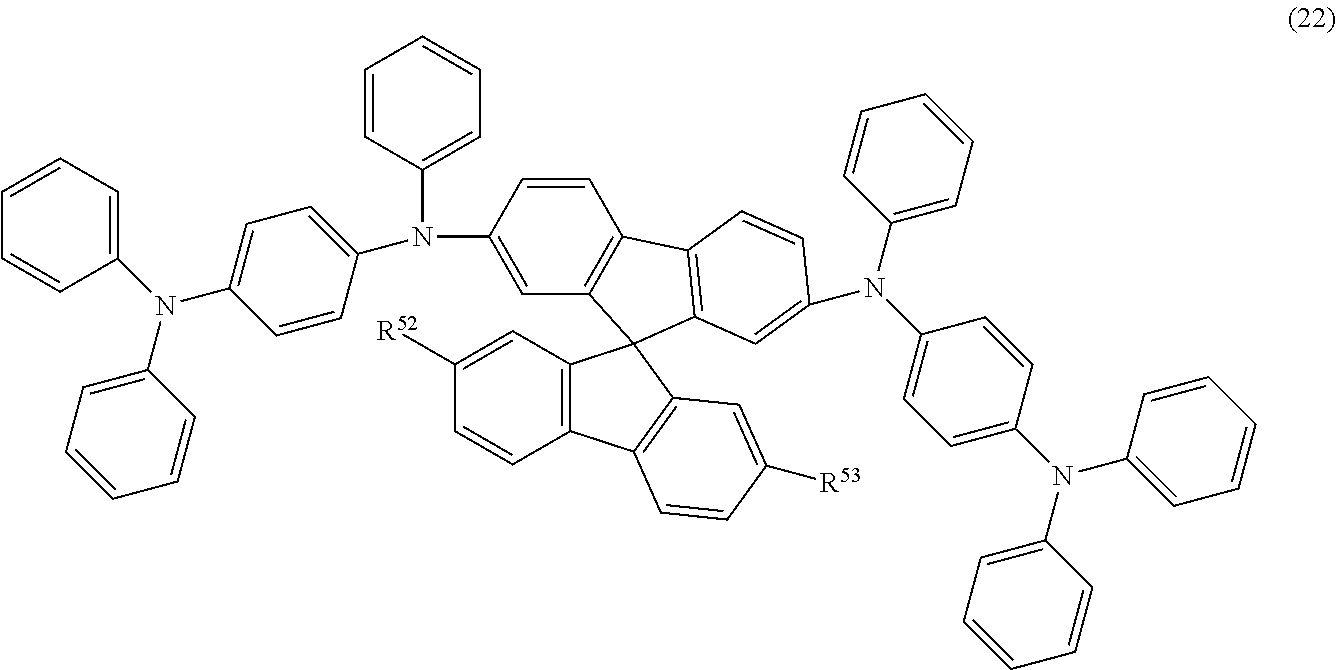
One feature of the present invention is a spirofluorene derivative represented by General Formula 23. (In the formula, each of R54 and R55 is hydrogen or an alkyl group having 1 to 4 carbon atoms and may be identical or different.)

One feature of the present invention is a spirofluorene derivative represented by General Formula 24. (In the formula, each of R56 and R57 is hydrogen or an alkyl group having 1 to 4 carbon atoms and may be identical or different.)
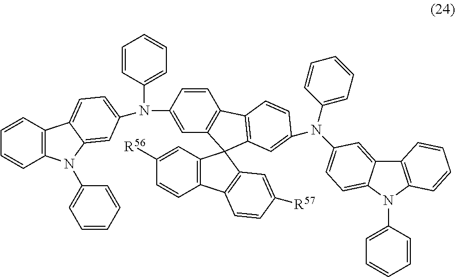
One feature of the present invention is a spirofluorene derivative represented by Structural Formula 25.

One feature of the present invention is a spirofluorene derivative represented by Structural Formula (66).

One feature of the present invention is a spirofluorene derivative represented by Structural Formula (35).

One feature of the present invention is a spirofluorene derivative represented by Structural Formula (26).

One feature of the present invention is a spirofluorene derivative represented by Structural Formula (67).

One feature of the present invention is a spirofluorene derivative represented by Structural Formula 30.

One feature of the present invention is a material for a light-emitting element containing any of the above-described spirofluorene derivatives.
One feature of the present invention is a light-emitting element containing any of the above-described spirofluorene derivatives.
One feature of the present invention is a light-emitting device including the above-described light-emitting element and a control circuit which controls light emission of the light-emitting element.
One feature of the present invention is an electronic device including a display portion using the above-described light-emitting element and a control circuit which controls the light-emitting element.
A spirofluorene derivative of the present invention is a novel material having a high glass transition temperature (Tg) and a wide energy gap. In addition, a spirofluorene derivative of the present invention is a material for a light-emitting element, which has a high Tg and a wide band gap.
A spirofluorene derivative of the present invention is a novel material having a sufficient hole transporting property, a sufficiently large energy gap, and a high glass transition temperature (Tg) as a material forming a hole transporting layer.
A spirofluorene derivative of the present invention is a material for a light-emitting element, which has a sufficient hole transporting property, a sufficiently large energy gap, and a high glass transition temperature (Tg) as a material forming a hole transporting layer.
A light-emitting element of the present invention is a light-emitting element having high heat resistance, and also a light-emitting element having high light-emitting efficiency.
A light-emitting device of the present invention is a light-emitting device having high heat resistance, and also a light-emitting device having small power consumption.
An electronic device of the present invention is an electronic device having high heat resistance, and also an electronic device having small power consumption.
In the accompanying drawings:
Embodiment modes and examples of the present invention will be described with reference to the drawings. Note that it is easily understood by those skilled in the art that the invention is not limited to the following descriptions, and various changes may be made in forms and details without departing from the spirit and the scope of the invention. Therefore, the invention should not be limited to the descriptions of the embodiment modes and examples below.
A spirofluorene derivative of the present invention is shown in General Formula 1.

In the formula, R1 is any one of hydrogen, an alkyl group having 1 to 4 carbon atoms, or a group represented by General Formula 2. As the alkyl group having 1 to 4 carbon atoms, specifically, a methyl group, an ethyl group, an n-propyl group, an iso-propyl group, an n-butyl group, an iso-butyl group, a sec-butyl group, a t-butyl group, or the like can be used. As R1, any one of hydrogen, a t-butyl group, or a group represented by General Formula 2 is particularly preferable.

In the formula, each of R2 and R3 is either hydrogen or an alkyl group having 1 to 4 carbon atoms. As the alkyl group having 1 to 4 carbon atoms, specifically, a methyl group, an ethyl group, an n-propyl group, an iso-propyl group, an n-butyl group, an iso-butyl group, a sec-butyl group, a t-butyl group, or the like can be used. As R2 and R3, hydrogen or a t-butyl group is particularly preferable. R2 and R3 may be identical or different.
R4 is an aryl group having 6 to 15 carbon atoms. As the aryl group having 6 to 15 carbon atoms, a phenyl group, an o-biphenyl group, an m-biphenyl group, a p-biphenyl group, a fluorene-2-yl group, a 9,9-dimethylfluorene-2-yl group, a naphthyl group, or the like can be used. In order to make the spirofluorene derivative represented by General Formula 1 into a compound having a larger energy gap, R4 is preferably a group which does not have a condensed ring skeleton, selected from among aryl groups having 6 to 15 carbon atoms. Each of the aryl groups having 6 to 15 carbon atoms may have a substituent, and an alkyl group having 1 to 4 carbon atoms or an aryl group having 6 to 15 carbon atoms can be used as the substituent. As the alkyl group having 1 to 4 carbon atoms, specifically, a methyl group, an ethyl group, an n-propyl group, an iso-propyl group, an n-butyl group, an iso-butyl group, a sec-butyl group, a t-butyl group, or the like can be used. As the aryl group having 6 to 15 carbon atoms, specifically, a phenyl group, an o-biphenyl group, an m-biphenyl group, a p-biphenyl group, a fluorene-2-yl group, a 9,9-dimethylfluorene-2-yl group, a naphthyl group, or the like can be used. As R4, an unsubstituted phenyl group is particularly preferable.
In the formula, each of R5 and R6 is any one of hydrogen, an alkyl group having 1 to 4 carbon atoms, or an aryl group having 6 to 15 carbon atoms. As the alkyl group having 1 to 4 carbon atoms, specifically, a methyl group, an ethyl group, an n-propyl group, an iso-propyl group, an n-butyl group, an iso-butyl group, a sec-butyl group, a t-butyl group, or the like can be used. As the aryl group having 6 to 15 carbon atoms, a phenyl group, an o-biphenyl group, an m-biphenyl group, a p-biphenyl group, a fluorene-2-yl group, a 9,9-dimethylfluorene-2-yl group, a naphthyl group, or the like can be used. As R5 and R6, hydrogen is particularly preferable. Note that R5 and R6 may be identical or different and may have a substituent or no substituent.
A spirofluorene derivative of the present invention is shown in General Formula 3.

In the formula, R7 is any one of hydrogen, an alkyl group having 1 to 4 carbon atoms, or a group represented by General Formula 4. As the alkyl group having 1 to 4 carbon atoms, specifically, a methyl group, an ethyl group, an n-propyl group, an iso-propyl group, an n-butyl group, an iso-butyl group, a sec-butyl group, a t-butyl group, or the like can be used. As R7, any one of hydrogen, a t-butyl group, or a group represented by General Formula 4 is particularly preferable.

In the formula, each of R8 and R9 is either hydrogen or an alkyl group having 1 to 4 carbon atoms. As the alkyl group having 1 to 4 carbon atoms, specifically, a methyl group, an ethyl group, an n-propyl group, an iso-propyl group, an n-butyl group, an iso-butyl group, a sec-butyl group, a t-butyl group, or the like can be used. As R8 and R9, hydrogen or a t-butyl group is particularly preferable. Note that R8 and R9 may be identical or different.
R10 is an aryl group having 6 to 15 carbon atoms. As the aryl group having 6 to 15 carbon atoms, a phenyl group, an o-biphenyl group, an m-biphenyl group, a p-biphenyl group, a fluorene-2-yl group, a 9,9-dimethylfluorene-2-yl group, a naphthyl group, or the like can be used. In order to make the spirofluorene derivative represented by General Formula 3 into a compound having a larger energy gap, R10 is preferably a group which does not have a condensed ring skeleton. Each of the aryl groups having 6 to 15 carbon atoms may have a substituent, and an alkyl group having 1 to 4 carbon atoms or an aryl group having 6 to 15 carbon atoms can be used as the substituent. As the alkyl group having 1 to 4 carbon atoms, specifically, a methyl group, an ethyl group, an n-propyl group, an iso-propyl group, an n-butyl group, an iso-butyl group, a sec-butyl group, a t-butyl group, or the like can be used. As the aryl group having 6 to 15 carbon atoms, specifically, a phenyl group, an o-biphenyl group, an m-biphenyl group, a p-biphenyl group, a fluorene-2-yl group, a 9,9-dimethylfluorene-2-yl group, a naphthyl group, or the like can be used. As R10, an unsubstituted phenyl group is particularly preferable.
In the formula, each of R11 and R12 is any one of hydrogen, an alkyl group having 1 to 4 carbon atoms, or an aryl group having 6 to 15 carbon atoms. As the alkyl group having 1 to 4 carbon atoms, specifically, a methyl group, an ethyl group, an n-propyl group, an iso-propyl group, an n-butyl group, an iso-butyl group, a sec-butyl group, a t-butyl group, or the like can be used. As the aryl group having 6 to 15 carbon atoms, a phenyl group, an o-biphenyl group, an m-biphenyl group, a p-biphenyl group, a fluorene-2-yl group, a 9,9-dimethylfluorene-2-yl group, a naphthyl group, or the like can be used. As R11 and R12, hydrogen is particularly preferable. Note that R11 and R12 may be identical or different and may have a substituent or no substituent.
A spirofluorene derivative of the present invention is represented by General Formula 5.

In the formula, R13 is any one of hydrogen, an alkyl group having 1 to 4 carbon atoms, or a group represented by General Formula 6. As the alkyl group having 1 to 4 carbon atoms, specifically, a methyl group, an ethyl group, an n-propyl group, an iso-propyl group, an n-butyl group, an iso-butyl group, a sec-butyl group, a t-butyl group, or the like can be used. As R13, any one of hydrogen, a t-butyl group, or a group represented by General Formula 6 is particularly preferable.

In the formula, each of R14 and R15 is either hydrogen or an alkyl group having 1 to 4 carbon atoms. As the alkyl group having 1 to 4 carbon atoms, specifically, a methyl group, an ethyl group, an n-propyl group, an iso-propyl group, an n-butyl group, an iso-butyl group, a sec-butyl group, a t-butyl group, or the like can be used. As R14 and R15, hydrogen or a t-butyl group is particularly preferable. Note that R14 and R15 may be identical or different.
R16 is an aryl group having 6 to 15 carbon atoms. As the aryl group having 6 to 15 carbon atoms, a phenyl group, an o-biphenyl group, an m-biphenyl group, a p-biphenyl group, a fluorene-2-yl group, a 9,9-dimethylfluorene-2-yl group, a naphthyl group, or the like can be used. In order to make the spirofluorene derivative represented by General Formula 5 into a compound having a larger energy gap, R16 is preferably a group which does not have a condensed ring skeleton. Each of the aryl groups having 6 to 15 carbon atoms may have a substituent, and an alkyl group having 1 to 4 carbon atoms or an aryl group having 6 to 15 carbon atoms can be used as the substituent. As the alkyl group having 1 to 4 carbon atoms, specifically, a methyl group, an ethyl group, an n-propyl group, an iso-propyl group, an n-butyl group, an iso-butyl group, a sec-butyl group, a t-butyl group, or the like can be used. As the aryl group having 6 to 15 carbon atoms, specifically, a phenyl group, an o-biphenyl group, an m-biphenyl group, a p-biphenyl group, a fluorene-2-yl group, a 9,9-dimethylfluorene-2-yl group, a naphthyl group, or the like can be used. As R16, an unsubstituted phenyl group is particularly preferable.
In the formula, R17 is any one of hydrogen, an alkyl group having 1 to 4 carbon atoms, or an aryl group having 6 to 15 carbon atoms. As the alkyl group having 1 to 4 carbon atoms, specifically, a methyl group, an ethyl group, an n-propyl group, an iso-propyl group, an n-butyl group, an iso-butyl group, a sec-butyl group, a t-butyl group, or the like can be used. As the aryl group having 6 to 15 carbon atoms, a phenyl group, an o-biphenyl group, an m-biphenyl group, a p-biphenyl group, a fluorene-2-yl group, a 9,9-dimethylfluorene-2-yl group, a naphthyl group, or the like can be used. As R17, hydrogen is particularly preferable. Note that R17 may have a substituent or no substituent.
In the formula, R18 is either an alkyl group having 1 to 4 carbon atoms or an aryl group having 6 to 15 carbon atoms. As the alkyl group having 1 to 4 carbon atoms, specifically, a methyl group, an ethyl group, an n-propyl group, an iso-propyl group, an n-butyl group, an iso-butyl group, a sec-butyl group, a t-butyl group, or the like can be used. As the aryl group having 6 to 15 carbon atoms, a phenyl group, an o-biphenyl group, an m-biphenyl group, a p-biphenyl group, a fluorene-2-yl group, a 9,9-dimethylfluorene-2-yl group, a naphthyl group, or the like can be used. In order to make the spirofluorene derivative represented by General Formula 5 into a compound having a larger energy gap, R18 is preferably a group which does not have a condensed ring skeleton, which is selected from among alkyl groups having 1 to 4 carbon atoms and aryl groups having 6 to 15 carbon atoms. Each of the aryl groups having 6 to 15 carbon atoms may have a substituent, and an alkyl group having 1 to 4 carbon atoms or an aryl group having 6 to 15 carbon atoms can be used as the substituent. As the alkyl group having 1 to 4 carbon atoms serving as a substituent, specifically, a methyl group, an ethyl group, an n-propyl group, an iso-propyl group, an n-butyl group, an iso-butyl group, a sec-butyl group, a t-butyl group, or the like can be used. As the aryl group having 6 to 15 carbon atoms, specifically, a phenyl group, an o-biphenyl group, an m-biphenyl group, a p-biphenyl group, a fluorene-2-yl group, a 9,9-dimethylfluorene-2-yl group, a naphthyl group, or the like can be used. As R18, an unsubstituted phenyl group is particularly preferable.
A spirofluorene derivative of the present invention is represented by General Formula 7.

In the formula, R19 is any one of hydrogen, an alkyl group having 1 to 4 carbon atoms, or a group represented by General Formula 8. As the alkyl group having 1 to 4 carbon atoms, specifically, a methyl group, an ethyl group, an n-propyl group, an iso-propyl group, an n-butyl group, an iso-butyl group, a sec-butyl group, a t-butyl group, or the like can be used. As R19, any one of hydrogen, a t-butyl group, or a group represented by General Formula 8 is particularly preferable.

In the formula, each of R20 and R21 is either hydrogen or an alkyl group having 1 to 4 carbon atoms. As the alkyl group having 1 to 4 carbon atoms, specifically, a methyl group, an ethyl group, an n-propyl group, an iso-propyl group, an n-butyl group, an iso-butyl group, a sec-butyl group, a t-butyl group, or the like can be used. As R20 and R21, hydrogen or a t-butyl group is particularly preferable. Note that R20 and R21 may be identical or different.
R22 is any one of hydrogen, an alkyl group having 1 to 4 carbon atoms, or an aryl group having 6 to 15 carbon atoms. As the alkyl group having 1 to 4 carbon atoms, specifically, a methyl group, an ethyl group, an n-propyl group, an iso-propyl group, an n-butyl group, an iso-butyl group, a sec-butyl group, a t-butyl group, or the like can be used. As the aryl group having 6 to 15 carbon atoms, specifically, a phenyl group, an o-biphenyl group, an m-biphenyl group, a p-biphenyl group, a fluorene-2-yl group, a 9,9-dimethylfluorene-2-yl group, a naphthyl group, or the like can be used. In order to make the spirofluorene derivative represented by General Formula 7 into a compound having a larger energy gap, R22 is preferably a group which does not have a condensed ring skeleton. As R22, hydrogen is particularly preferable.
In the formula, each of R23 and R24 is any one of hydrogen, an alkyl group having 1 to 4 carbon atoms, or an aryl group having 6 to 15 carbon atoms. As the alkyl group having 1 to 4 carbon atoms, specifically, a methyl group, an ethyl group, an n-propyl group, an iso-propyl group, an n-butyl group, an iso-butyl group, a sec-butyl group, a t-butyl group, or the like can be used. As the aryl group having 6 to 15 carbon atoms, a phenyl group, an o-biphenyl group, an m-biphenyl group, a p-biphenyl group, a fluorene-2-yl group, a 9,9-dimethylfluorene-2-yl group, a naphthyl group, or the like can be used. As R23 and R24, hydrogen is particularly preferable. Note that R23 and R24 may be identical or different and may have a substituent or no substituent.
A spirofluorene derivative of the present invention is represented by General Formula 9.

In the formula, R25 is any one of hydrogen, an alkyl group having 1 to 4 carbon atoms, or a group represented by General Formula 10. As the alkyl group having 1 to 4 carbon atoms, specifically, a methyl group, an ethyl group, an n-propyl group, an iso-propyl group, an n-butyl group, an iso-butyl group, a sec-butyl group, a t-butyl group, or the like can be used. As R25, any one of hydrogen, a t-butyl group, or a group represented by General Formula 10 is particularly preferable.

In the formula, each of R26 and R27 is either hydrogen or an alkyl group having 1 to 4 carbon atoms. As the alkyl group having 1 to 4 carbon atoms, specifically, a methyl group, an ethyl group, an n-propyl group, an iso-propyl group, an n-butyl group, an iso-butyl group, a sec-butyl group, a t-butyl group, or the like can be used. As R26 and R27, hydrogen or a t-butyl group is particularly preferable. Note that R26 and R27 may be identical or different.
R28 is any one of hydrogen, an alkyl group having 1 to 4 carbon atoms, or an aryl group having 6 to 15 carbon atoms. As the alkyl group having 1 to 4 carbon atoms, specifically, a methyl group, an ethyl group, an n-propyl group, an iso-propyl group, an n-butyl group, an iso-butyl group, a sec-butyl group, a t-butyl group, or the like can be used. As the aryl group having 6 to 15 carbon atoms, specifically, a phenyl group, an o-biphenyl group, an m-biphenyl group, a p-biphenyl group, a fluorene-2-yl group, a 9,9-dimethylfluorene-2-yl group, a naphthyl group, or the like can be used. In order to make the spirofluorene derivative represented by General Formula 9 into a compound having a larger energy gap, R28 is preferably a group which does not have a condensed ring skeleton. As R28, hydrogen is particularly preferable.
In the formula, each of R29 and R30 is any one of hydrogen, an alkyl group having 1 to 4 carbon atoms, or an aryl group having 6 to 15 carbon atoms. As the alkyl group having 1 to 4 carbon atoms, specifically, a methyl group, an ethyl group, an n-propyl group, an iso-propyl group, an n-butyl group, an iso-butyl group, a sec-butyl group, a t-butyl group, or the like can be used. As the aryl group having 6 to 15 carbon atoms, a phenyl group, an o-biphenyl group, an m-biphenyl group, a p-biphenyl group, a fluorene-2-yl group, a 9,9-dimethylfluorene-2-yl group, a naphthyl group, or the like can be used. As R29 and R30, hydrogen is particularly preferable. Note that R29 and R30 may be identical or different and may have a substituent or no substituent.
A spirofluorene derivative of the present invention is represented by General Formula 11.

In the formula, R31 is any one of hydrogen, an alkyl group having 1 to 4 carbon atoms, or a group represented by General Formula 12. As the alkyl group having 1 to 4 carbon atoms, specifically, a methyl group, an ethyl group, an n-propyl group, an iso-propyl group, an n-butyl group, an iso-butyl group, a sec-butyl group, a t-butyl group, or the like can be used. As R31, any one of hydrogen, a t-butyl group, or a group represented by General Formula 12 is particularly preferable.

In the formula, each of R32 and R33 is either hydrogen or an alkyl group having 1 to 4 carbon atoms. As the alkyl group having 1 to 4 carbon atoms, specifically, a methyl group, an ethyl group, an n-propyl group, an iso-propyl group, an n-butyl group, an iso-butyl group, a sec-butyl group, a t-butyl group, or the like can be used. As R32 and R33, hydrogen or a t-butyl group is particularly preferable. Note that R32 and R33 may be identical or different.
R34 is any one of hydrogen, an alkyl group having 1 to 4 carbon atoms, or an aryl group having 6 to 15 carbon atoms. As the alkyl group having 1 to 4 carbon atoms, specifically, a methyl group, an ethyl group, an n-propyl group, an iso-propyl group, an n-butyl group, an iso-butyl group, a sec-butyl group, a t-butyl group, or the like can be used. As the aryl group having 6 to 15 carbon atoms, specifically, a phenyl group, an o-biphenyl group, an m-biphenyl group, a p-biphenyl group, a fluorene-2-yl group, a 9,9-dimethylfluorene-2-yl group, a naphthyl group, or the like can be used. In order to make the spirofluorene derivative represented by General Formula 11 into a compound having a larger energy gap, R34 is preferably a group which does not have a condensed ring skeleton. As R34, hydrogen is particularly preferable.
In the formula, R35 is any one of hydrogen, an alkyl group having 1 to 4 carbon atoms, or an aryl group having 6 to 15 carbon atoms. As the alkyl group having 1 to 4 carbon atoms, specifically, a methyl group, an ethyl group, an n-propyl group, an iso-propyl group, an n-butyl group, an iso-butyl group, a sec-butyl group, a t-butyl group, or the like can be used. As the aryl group having 6 to 15 carbon atoms, a phenyl group, an o-biphenyl group, an m-biphenyl group, a p-biphenyl group, a fluorene-2-yl group, a 9,9-dimethylfluorene-2-yl group, a naphthyl group, or the like can be used. As R35, hydrogen is particularly preferable. Note that R35 may have a substituent or no substituent.
In the formula, R36 is any one of hydrogen, an alkyl group having 1 to 4 carbon atoms, or an aryl group having 0.6 to 15 carbon atoms. As the alkyl group having 1 to 4 carbon atoms serving as a substituent, specifically, a methyl group, an ethyl group, an n-propyl group, an iso-propyl group, an n-butyl group, an iso-butyl group, a sec-butyl group, a t-butyl group, or the like can be used. As the aryl group having 6 to 15 carbon atoms, specifically, a phenyl group, an o-biphenyl group, an m-biphenyl group, a p-biphenyl group, a fluorene-2-yl group, a 9,9-dimethylfluorene-2-yl group, a naphthyl group, or the like can be used. In order to make the spirofluorene derivative represented by General Formula 11 into a compound having a larger energy gap, R36 is preferably a group which does not have a condensed ring skeleton. As R36, hydrogen is particularly preferable.
A spirofluorene derivative of the present invention is represented by General Formula 13.

In the formula, R37 is any one of hydrogen, an alkyl group having 1 to 4 carbon atoms, or a group represented by General Formula 14 (N-{4-(N′,N′-diphenyl)anilino}aniline). As the alkyl group having 1 to 4 carbon atoms, specifically, a methyl group, an ethyl group, an n-propyl group, an iso-propyl group, an n-butyl group, an iso-butyl group, a sec-butyl group, a t-butyl group, or the like can be used. As R37, any one of hydrogen, a t-butyl group, or a group represented by General Formula 14 is particularly preferable.

In the formula, each of R38 and R39 is either hydrogen or an alkyl group having 1 to 4 carbon atoms. As the alkyl group having 1 to 4 carbon atoms, specifically, a methyl group, an ethyl group, an n-propyl group, an iso-propyl group, an n-butyl group, an iso-butyl group, a sec-butyl group, a t-butyl group, or the like can be used. As R38 and R39, hydrogen or a t-butyl group is particularly preferable. Note that R38 and R39 may be identical or different.
A spirofluorene derivative of the present invention is represented by General Formula 15.

In the formula, R40 is any one of hydrogen, an alkyl group having 1 to 4 carbon atoms, or a group represented by General Formula 16 (a {4-(9-carbazolyl)phenyl}phenylamino group). As the alkyl group having 1 to 4 carbon atoms, specifically, a methyl group, an ethyl group, an n-propyl group, an iso-propyl group, an n-butyl group, an iso-butyl group, a sec-butyl group, a t-butyl group, or the like can be used. As R40, any one of hydrogen, a t-butyl group, or a group represented by General Formula 16 is particularly preferable.

In the formula, each of R41 and R42 is either hydrogen or an alkyl group having 1 to 4 carbon atoms. As the alkyl group having 1 to 4 carbon atoms, specifically, a methyl group, an ethyl group, an n-propyl group, an iso-propyl group, an n-butyl group, an iso-butyl group, a sec-butyl group, a t-butyl group, or the like can be used. As R41 and R42, hydrogen or a t-butyl group is particularly preferable. Note that R41 and R42 may be identical or different.
A spirofluorene derivative of the present invention is represented by General Formula 17.

In the formula, R43 is any one of hydrogen, an alkyl group having 1 to 4 carbon atoms, or a group represented by General Formula 18 (a [3-(9-phenylcarbazolyl)]phenylamino group). As the alkyl group having 1 to 4 carbon atoms, specifically, a methyl group, an ethyl group, an n-propyl group, an iso-propyl group, an n-butyl group, an iso-butyl group, a sec-butyl group, a t-butyl group, or the like can be used. As R43, any one of hydrogen, a t-butyl group, or a group represented by General Formula 18 is particularly preferable.

In the formula, each of R44 and R45 is either hydrogen or an alkyl group having 1 to 4 carbon atoms. As the alkyl group having 1 to 4 carbon atoms, specifically, a methyl group, an ethyl group, an n-propyl group, an iso-propyl group, an n-butyl group, an iso-butyl group, a sec-butyl group, a t-butyl group, or the like can be used. As R44 and R45, hydrogen or a t-butyl group is particularly preferable. Note that R44 and R45 may be identical or different.
A spirofluorene derivative of the present invention is represented by General Formula 19.

In the formula, each of R46 and R47 is either hydrogen or an alkyl group having 1 to 4 carbon atoms. As the alkyl group having 1 to 4 carbon atoms, specifically, a methyl group, an ethyl group, an n-propyl group, an iso-propyl group, an n-butyl group, an iso-butyl group, a sec-butyl group, a t-butyl group, or the like can be used. As R46 and R47, hydrogen or a t-butyl group is particularly preferable. Note that R46 and R47 may be identical or different.
A spirofluorene derivative of the present invention is represented by General Formula 20.

In the formula, each of R48 and R49 is either hydrogen or an alkyl group having 1 to 4 carbon atoms. As the alkyl group having 1 to 4 carbon atoms, specifically, a methyl group, an ethyl group, an n-propyl group, an iso-propyl group, an n-butyl group, an iso-butyl group, a sec-butyl group, a t-butyl group, or the like can be used. As R48 and R49, hydrogen or a t-butyl group is particularly preferable. Note that R48 and R49 may be identical or different.
A spirofluorene derivative of the present invention is represented by General Formula 21.

In the formula, each of R50 and R51 is either hydrogen or an alkyl group having 1 to 4 carbon atoms. As the alkyl group having 1 to 4 carbon atoms, specifically, a methyl group, an ethyl group, an n-propyl group, an iso-propyl group, an n-butyl group, an iso-butyl group, a sec-butyl group, a t-butyl group, or the like can be used. As R50 and R51, hydrogen or a t-butyl group is particularly preferable. Note that R50 and R51 may be identical or different.
A spirofluorene derivative of the present invention is represented by General Formula 22.

In the formula, each of R52 and R53 is either hydrogen or an alkyl group having 1 to 4 carbon atoms. As the alkyl group having 1 to 4 carbon atoms, specifically, a methyl group, an ethyl group, an n-propyl group, an iso-propyl group, an n-butyl group, an iso-butyl group, a sec-butyl group, a t-butyl group, or the like can be used. As R52 and R53, hydrogen or a t-butyl group is particularly preferable. Note that R52 and R53 may be identical or different.
A spirofluorene derivative of the present invention is represented by General Formula 23.

In the formula, each of R54 and R55 is either hydrogen or an alkyl group having 1 to 4 carbon atoms. As the alkyl group having 1 to 4 carbon atoms, specifically, a methyl group, an ethyl group, an n-propyl group, an iso-propyl group, an n-butyl group, an iso-butyl group, a sec-butyl group, a t-butyl group, or the like can be used. As R54 and R55, hydrogen or a t-butyl group is particularly preferable. Note that R54 and R55 may be identical or different.
A spirofluorene derivative of the present invention is represented by General Formula 24.

In the formula, each of R56 and R57 is either hydrogen or an alkyl group having 1 to 4 carbon atoms. As the alkyl group having 1 to 4 carbon atoms, specifically, a methyl group, an ethyl group, an n-propyl group, an iso-propyl group, an n-butyl group, an iso-butyl group, a sec-butyl group, a t-butyl group, or the like can be used. As R56 and R57, hydrogen or a t-butyl group is particularly preferable. Note that R56 and R57 may be identical or different.
As a spirofluorene derivative of the present invention, spirofluorene derivatives represented by Structural Formulas 25 to 110 can be used. In the formulas, Me indicates a methyl group; Et, an ethyl group; i-Pro, an iso-propyl group; n-Pro, an n-propyl group; n-Bu, an n-butyl group; i-Bu, an iso-butyl group; s-Bu, a sec-butyl group; and t-Bu, a t-butyl group. Note that a spirofluorene derivative of the present invention is not limited thereto.


A spirofluorene derivative of the present invention having any of the above-described structures is a novel material having a high glass transition temperature (Tg). In addition, a spirofluorene derivative of the present invention having any of the above-described structures is a novel material having a wide energy gap. Further, a spirofluorene derivative of the present invention having any of the above-described structures is a novel material having a high Tg and a wide band gap.
Since a spirofluorene derivative of the present invention having any of the above-described structures has a low HOMO (Highest Occupied Molecular Orbital) level, it has a sufficient hole transporting property capable of being used for a hole transporting layer of a light-emitting element in which a layer containing an organic compound is interposed between a pair of electrodes and which emits light by being applied with current. Accordingly, a spirofluorene derivative of the present invention having any of the above-described structures can be favorably used as a material for a light-emitting element.
In addition, since a spirofluorene derivative of the present invention having any of the above-described structures has a high LUMO (Lowest Unoccupied Molecular Orbital) level, it has a sufficient hole injecting property capable of being used for a hole injecting layer of a light-emitting element in which a layer containing an organic compound is interposed between a pair of electrodes and which emits light by being applied with current. Accordingly, a spirofluorene derivative of the present invention having any of the above-described structures can be favorably used as a material for a light-emitting element.
The spirofluorene derivatives described in Embodiment Mode 1 are electrochemically stable materials, since they have tolerance to a cycle of oxidation and reduction subsequent to the oxidation.
A structure of a light-emitting element in the present invention is such that a layer containing an organic compound is interposed between a pair of electrodes. Note that the element structure is not particularly limited and can be selected as appropriate in accordance with its purposes.
For the anode, a metal, an alloy, a conductive compound, a mixture thereof, or the like having a high work function (specifically, of 4.0 eV or higher) is preferably used. Specifically, indium tin oxide (hereinafter referred to as ITO), indium tin oxide containing silicon, indium oxide containing zinc oxide (ZnO), or the like can be used. A film of these conductive metal oxides is generally formed by sputtering, but may be formed by a sol-gel method or the like. Alternatively, gold (Au), platinum (Pt), nickel (Ni), tungsten (W), chromium (Cr), molybdenum (Mo), iron (Fe), cobalt (Co), copper (Cu), palladium (Pd), nitride of a metal material (for example, titanium nitride (TiN)), or the like can be used.
On the other hand, for the cathode, a metal, an alloy, a conductive compound, a mixture thereof, or the like having a low work function (specifically, of 3.8 eV or lower) is preferably used. Specifically, a metal belonging to Group 1 or 2 of the periodic table, that is, an alkali metal such as lithium (Li) or cesium (Cs); an alkaline earth metal such as magnesium (Mg), calcium (Ca), or strontium (Sr); an alloy containing these (such as MgAg or AlLi) a rare-earth metal such as europium (Er) or ytterbium (Yb); an alloy containing these; or the like can be used. Note that when using an electron injecting layer having a high electron injecting property, the cathode can also be formed using a material having a high work function, that is, a material generally used for the anode. For example, the cathode can be formed of a metal such as Al or Ag or of a conductive inorganic compound such as ITO.
The layer containing an organic compound 102 can be formed using either a low molecular material or a high molecular material. In addition, the material forming the layer containing an organic compound 102 is not limited to a material containing only an organic compound material, and may partially contain an inorganic compound material. A layer containing an organic compound is generally formed by appropriately combining functional layers having respective functions such as a hole injecting layer, a hole transporting layer, a hole blocking layer, a light-emitting layer, an electron transporting layer, and an electron injecting layer; however, the layer containing an organic compound may include a layer having two or more functions of the above-described functional layers. In this embodiment mode, a layered structure including a hole injecting layer, a hole transporting layer, a light-emitting layer, an electron transporting layer, and an electron injecting layer is employed for the layer containing an organic compound.
In addition, the layer containing an organic compound 102 can be formed by either a wet method or a dry method, such as an evaporation method, an ink-jet method, a spin coating method, or a dip coating method.
The spirofluorene derivative described in Embodiment Mode 1 is a material having a high glass transition temperature (Tg) and high heat resistance. Since the layer containing an organic compound 102 of a light-emitting element of the present invention contains the spirofluorene derivative described in Embodiment Mode 1, the light-emitting element can have high heat resistance. In addition, since the spirofluorene derivative described in Embodiment Mode 1 has a wide energy gap, it is difficult for energy to transfer from another layer, and a light-emitting element having high light-emitting efficiency and color purity can be obtained. In a light emitting layer of a light-emitting element exhibiting blue light emission, since an energy gap of a host material in a light-emitting layer is slightly larger than that of blue light emitting material, energy transfer to a layer adjacent to the light-emitting layer has been a severe problem. However, since the spirofluorene derivative described in Embodiment Mode 1 has a wide energy gap, even in a blue light-emitting element, excitation energy transfer from a light-emitting layer is not a concern. The spirofluorene derivative described in Embodiment Mode 1 can also be favorably used for a light-emitting element emitting another color such as red or green.
Since the spirofluorene derivative described in Embodiment Mode 1 has a relatively low HOMO (Highest Occupied Molecular Orbital) level and a sufficient hole transporting property, it is suitable as a material for a hole transporting layer. In addition, since the spirofluorene derivative described in Embodiment Mode 1 has a sufficient hole transporting property and a wide energy gap, it can be particularly favorably used as a material for a hole transporting layer which is often formed adjacent to a light-emitting layer. Further, since the spirofluorene derivative described in Embodiment Mode 1 can be favorably used as a host material which disperses a light-emitting material in a light-emitting layer and has a wide band gap, it can be favorably used as a host material which disperses a blue light-emitting material having a relatively wide band gap. The spirofluorene derivative described in Embodiment Mode 1 can also be favorably used for a light-emitting element emitting another color such as red or green.
A light-emitting element of the present invention in this embodiment mode uses a spirofluorene derivative described in Embodiment Mode 1 for a hole transporting layer. There is no particular limitation on other functional layers in the layer containing an organic compound 102. In addition, since the spirofluorene derivative described in Embodiment Mode 1 has a high LUMO (Lowest Unoccupied Molecular Orbital) level, the passing-through of electrons can be prevented. Due to this, by using a spirofluorene derivative for a hole transporting layer which is in contact with a light-emitting layer, electrons and holes can efficiently be recombined in the light-emitting layer, which improves light-emitting efficiency.
The hole injecting layer can be formed using a metal oxide such as vanadium oxide, molybdenum oxide, ruthenium oxide, or aluminum oxide, or a mixture in which such a metal oxide is mixed with an appropriate organic compound. Alternatively, if using an organic compound, a porphyrin-based compound is effective, and phthalocyanine (abbrev.: H2Pc), copper phthalocyanine (abbrev.: CuPc), or the like can be used. Further, a chemically-doped conductive high molecular compound can be used, such as polyethylene dioxythiophene (abbrev.: PEDOT) doped with polystyrene sulfonate (abbrev.: PSS), or polyaniline (abbrev.: PAni). The hole injecting layer is formed in contact with an anode. By using the hole injecting layer, a carrier injection barrier is reduced, and carriers are efficiently injected to a light-emitting layer, which results in reduction of driving voltage.
For the hole injecting layer, the spirofluorene derivative described in Embodiment Mode 1 can also be favorably used.
A composite material containing the spirofluorene derivative described in Embodiment Mode 1 and a metal oxide can be used for the hole injecting layer. As the metal oxide, an oxide of a transition metal is desirable, and oxide of a metal that belongs to any of Groups 4 to 8 of the periodic table is particularly desirable. Specifically, vanadium oxide, tantalum oxide, molybdenum oxide, tungsten oxide, rhenium oxide, and ruthenium oxide are preferable. In such composite materials, electrons are transferred between the spirofluorene derivative described in Embodiment Mode 1 and the metal oxide; accordingly, carrier density in the material is increased and beneficial effects such as an improvement in a hole injecting property can be obtained. Also, even when film thickness is increased, there is only a small increase in driving voltage. Even when a film thickness of this composite material is increased, the increase of driving voltage is small. Therefore, by adjusting the film thickness of a layer formed by using the composite material, a light-emitting element can be optically designed using a microcavity phenomenon or the like.
The hole transporting layer is formed using the spirofluorene derivative described in Embodiment Mode 1. The hole transporting layer is provided between the hole injecting layer and the light-emitting layer. Note that one hole transporting layer formed by using the spirofluorene derivative described in Embodiment Mode 1 may be formed such that the hole transporting layer has both functions of a hole injecting layer and a hole transporting layer. In this case, the hole injecting layer is not provided.
The light-emitting layer is formed using only a light-emitting material or using a host material into which a light-emitting material is dispersed. A substance which has favorable light-emitting efficiency and can emit light with a desired emission wavelength may be used as the light-emitting material. For example, in order to obtain red light emission, a substance which exhibits light emission having a peak of an emission spectrum at 600 nm to 680 nm can be used, such as 4-dicyanomethylene-2-isopropyl-6-[2-(1,1,7,7-tetramethyljulolidine-9-yl)ethenyl]-4H-pyran (abbrev.: 4-dicyanomethylene-2-methyl-6-[2-(1,1,7,7-tetramethyl-9-julolidine-9-yl)ethenyl]-4H-pyran (abbrev.: DCJT), 4-dicyanomethylene-2-tert-butyl-6-[2-(1,1,7,7-tetramethyljulolidine-9-yl)ethenyl]-4H-pyran (abbrev.: DCJTB), periflanthene, or 2,5-dicyano-1,4-bis[2-(10-methoxy-1,1,7,7-tetramethyljulolidine-9-yl)ethenyl]benzene. In order to obtain green light emission, a substance which exhibits light emission having a peak of an emission spectrum at 500 nm to 550 nm can be used, such as N,N′-dimethylquinacridon (abbrev.: DMQd), coumarin 6, coumarin 545T, or tris(8-quinolinolato)aluminum (abbrev.: Alq3). In order to obtain blue light emission, a substance which exhibits light emission having a peak of an emission spectrum at 420 nm to 500 nm can be used, such as 9,10-bis(2-naphthyl)-tert-butylanthracene (abbrev.: t-BuDNA), 9,9′-bianthryl, 9,10-diphenylanthracene (abbrev.: DPA), 9,10-bis(2-naphthyl)anthracene (abbrev.: DNA), bis(2-methyl-8-quinolinolato)-4-phenylphenolato-gallium (abbrev.: BGaq), or bis(2-methyl-8-quinolinolato)-4-phenylphenolato-aluminum (abbrev.: BAlq). In addition to the material which generates fluorescence as described above, a material which generates phosphorescence can also be used as a light-emitting material, such as bis[2-(3,5-bis(trifluoromethyl)phenyl)pyridinato-N,C2′]iridium(III)picolinate (abbrev.: Ir(CF3ppy)2(pic)), bis[2-(4,6-difluorophenyl)pyridinato-N,C2′]iridium(III)acetylacetonate (abbrev.: FIr(acac)), bis[2-(4,6-difluorophenyl)pyridinato-N,C2′]iridium(III)picolinate (FIr(pic)), or tris(2-phenylpyridinato-N,C2′)iridium (abbrev.: Ir(ppy)3). In addition, as the host material, an anthracene derivative such as 9,10-di(2-naphthyl)-2-tert-butylanthracene (abbrev.: t-BuDNA), a carbazole derivative such as 4,4′-di(N-carbazolyl)biphenyl (abbrev.: CBP), a metal complex such as bis[2-(2-hydroxyphenyl)pyridinato]zinc (abbrev.: Znpp2) or bis[2-(2-hydroxyphenyl)benzoxazolato]zinc (abbrev.: ZnBOX), or the like can be used. In the case where the light-emitting layer is formed using the host material into which the light-emitting material is dispersed, the light-emitting layer can be formed by adding the light-emitting material to the host material in a proportion of 0.001 wt % to 50 wt %, preferably, 0.03 wt % to 20 wt %. Note that in this case, it is preferable to combine materials such that an energy gap of the host material is larger than that of the light-emitting material.
In the case where the electron transporting layer is used, it is provided between the light-emitting layer and the electron injecting layer. An appropriate material is a typical metal complex such as tris(8-quinolinolato)aluminum (abbrev.: Alq3), tris(4-methyl-8-quinolinolato)aluminum (abbrev.: Almq3), bis(10-hydroxybenzo[h]-quinolinato)beryllium (abbrev.: BeBq2), bis(2-methyl-8-quinolinolato)-(4-hydroxy-biphenylyl)-aluminum (abbrev.: BAlq), bis[2-(2-hydroxyphenyl)-benzoxazolato]zinc (abbrev.: Zn(BOX)2), or bis[2-(2-hydroxyphenyl)-benzothiazolato]zinc (abbrev.: Zn(BTZ)2). Alternatively, a hydrocarbon-based compound such as 9,10-diphenylanthracene or 4,4′-bis(2,2-diphenylethenyl)biphenyl, or the like is preferable. Further alternatively, a triazole derivative such as 3-(4-tert-butylphenyl)-4-(4-ethylphenyl)-5-(4-biphenylyl)-1,2,4-triazole or a phenanthroline derivative such as bathophenanthroline or bathocuproin may be used.
There is no particular limitation on what electron injecting material is used for forming the electron injecting layer. Specifically, an alkali metal salt such as lithium fluoride, lithium oxide, or lithium chloride, an alkaline earth metal salt such as calcium fluoride, or the like is preferable. Alternatively, a layer in which a donor compound such as lithium is added to a so-called electron transporting material such as tris(8-quinolinolato)aluminum (abbrev.: Alq3) or bathocuproin (abbrev.: BCP) can be used. The electron injecting layer is formed in contact with the cathode. By using the electron injecting layer, a carrier injection barrier is reduced, and carriers, are efficiently injected to a light-emitting layer, which results in reduction of driving voltage.
In the case where the spirofluorene derivative described in Embodiment Mode 1 is used as a host material of the hole injecting layer or the light-emitting layer and another material is used for forming the hole transporting layer, there is no particular limitation on what material is used for the hole transporting layer, and 4,4′-bis[N-(1-naphthyl)-N-phenylamino]biphenyl (abbrev.: NPB), 4,4′-bis[N-(3-methylphenyl)-N-phenylamino]biphenyl (abbrev.: TPD), 4,4′,4″-tris(N,N-diphenylamino)triphenylamine (abbrev.: TDATA), 4,4′,4″-tris[N-(3-methylphenyl)-N-phenylamino]triphenylamine (abbrev.: MTDATA), 4,4′-bis{N-[4-(N,N-di-m-tolylamino)phenyl]-N-phenylamino}biphenyl (abbrev.: DNTPD), 1,3,5-tris[N,N-di(m-tolyl)amino]benzene (abbrev.: m-MTDAB), 4,4′,4″-tris(N-carbazolyl)triphenylamine (abbrev.: TCTA), phthalocyanine (abbrev.: H2Pc), copper phthalocyanine (abbrev.: CuPc), vanadyl phthalocyanine (abbrev.: VOPc), or the like can be used. The hole transporting layer may be formed by combining two or more layers of layers using the above-described materials or may be a layer having a multilayer structure in which a layer containing the spirofluorene derivative described in Embodiment Mode 1 and a layer using the above-described material are combined.
Although this embodiment describes a structure of a light-emitting element which provides light emission only from the light-emitting layer, a light-emitting element may be designed so as to provide light emission from not only a light-emitting layer but also another layer such as an electron transporting layer or a hole transporting layer. For example, light emission can be obtained from not only a light-emitting layer but also a transporting layer by adding a dopant which contributes to light emission to an electron transporting layer or a hole transporting layer. When light-emitting materials used for a light-emitting layer and a transporting layer have different light emission colors, a spectrum with emission colors thereof overlapped with each other can be obtained. If emission colors of the light-emitting layer and the transporting layer have the relationship of complementary colors, white light emission can be obtained.
Note that a light-emitting element of this embodiment mode has many variations obtained by changing a material for the first electrode 101 and a material for the second electrode 103 of FIG. 1 . When a light transmitting material is used for the first electrode 101, light can be emitted from the first electrode 101 side. When a light blocking (particularly, a reflective) material is used for the first electrode 101 and a light transmitting material is used for the second electrode 103, light can be emitted from the second electrode 103 side. Furthermore, when a light transmitting material is used for both the first electrode 101 and the second electrode 103, light can be emitted from both the first electrode 101 side and the second electrode 103 side.
A light-emitting device of the present invention and a method for manufacturing thereof will be described in this embodiment mode, with reference to FIGS. 2A to 2E and 3A to 3C . Note that an example of manufacturing an active matrix light-emitting device will be described in this embodiment mode; however, the present invention may of course also be applied to a passive matrix light-emitting device.
First, a first base insulating layer 51 a and a second base insulating layer 51 b are formed over a substrate 50. Then, a semiconductor layer 52 is formed over the second base insulating layer 51 b (FIG. 2A ).
As a material for the substrate 50, glass, quartz, plastic (such as polyimide, acrylic, polyethylene terephthalate, polycarbonate, polyacrylate, or polyether sulfone), or the like can be used. A substrate made from such a material may be used after being polished with CMP or the like, if necessary. In this embodiment mode, a glass substrate is used.
Providing the first base insulating layer 51 a and the second base insulating layer 51 b can prevent an element in the substrate 50 which adversely affects a characteristic of a semiconductor film, such as an alkali metal or an alkaline earth metal, from diffusing into the semiconductor layer. As materials for the first base insulating layer 51 a and the second base insulating layer 51 b, silicon oxide, silicon nitride, silicon oxide containing nitrogen, silicon nitride containing oxygen, or the like can be used. In this embodiment mode, the first base insulating layer 51 a is formed, using silicon nitride and the second base insulating layer 51 b is formed using silicon oxide. Although a base insulating film is formed using the first base insulating layer 51 a and the second base insulating layer 51 b in this embodiment mode, the base insulating film may be formed using a single layer or two or more layers. Further, when diffusion of an impurity from the substrate does not cause a problem, it is not necessary to provide a base insulating film.
In this embodiment mode, the semiconductor layer formed after the formation of the first and the second base insulating layers is obtained by crystallizing an amorphous silicon film by irradiation with a laser beam. Specifically, an amorphous silicon film is formed over the second base insulating layer 51 b to have a thickness of 25 to 100 nm (preferably, 30 to 60 nm). As a method for forming the amorphous silicon film, a method such as sputtering, reduced pressure CVD, or plasma CVD can be used. Then, heat treatment is conducted at 500° C. for 1 hour to dehydrogenate the film.
Next, the amorphous silicon film is crystallized by using a laser irradiation apparatus to form a crystalline silicon film. In the laser crystallization of this embodiment mode, an excimer laser is used, and a laser beam oscillated from the excimer laser is processed into a linear beam spot using an optical system. Then, the amorphous silicon film is irradiated with the linear beam spot so as to obtain the crystalline silicon film. This crystalline silicon film is used as a semiconductor layer. Note that the amorphous silicon film may also be used as is as a semiconductor layer.
Other methods of crystallizing an amorphous silicon film include a crystallization method using only heat treatment, and a crystallization method performing heat treatment by using a catalytic element for accelerating crystallization. As an element for accelerating crystallization, nickel, iron, palladium, tin, lead, cobalt, platinum, copper, gold, and the like can be given as examples. Compared to a case where crystallization is performed by only heat treatment, when crystallization is performed using this kind of element for accelerating crystallization, crystallization is performed at a lower temperature for a shorter time, so damage to the glass substrate and the like is small. When crystallization is performed by heat treatment only, a quartz substrate or the like which is resistant to heat may be used as the substrate 50.
Next, in order to control a threshold value, a minute amount of an impurity is added to the semiconductor layer, if necessary. That is, channel doping is performed. To obtain a required threshold value, an impurity (such as phosphorous or boron) having an N-type conductivity or a P-type conductivity is added to the semiconductor layer by ion doping or the like.
Then, the semiconductor layer is patterned into a prescribed shape, as shown in FIG. 2A , to obtain an island-like semiconductor layer 52. The patterning is performed by applying a photoresist to the semiconductor layer, exposing a predetermined mask shape, baking the shaped photoresist to form a resist mask over the semiconductor layer, and etching the semiconductor layer using the resist mask.
Next, a gate insulating layer 53 is formed to cover the semiconductor layer 52. The gate insulating layer 53 is formed by plasma CVD or sputtering to have a thickness of 40 to 150 nm using an insulating layer containing silicon. In this embodiment mode, the gate insulating layer 53 is formed using silicon oxide.
Next, a gate electrode 54 is formed over the gate insulating layer 53. The gate electrode 54 is formed using an element selected from among tantalum, tungsten, titanium, molybdenum, aluminum, copper, chromium, and niobium; or using an alloy material or a compound material containing the element as its main component. Further, a semiconductor film typified by a polycrystalline silicon film doped with an impurity element such as phosphorous may be used, or an AgPdCu alloy may be used.
Although the gate electrode 54 is formed with a single layer in this embodiment mode, it may be formed to have a laminated structure including two or more layers, such as a lower layer made from tungsten and an upper layer made from molybdenum. When the gate electrode is formed to include a laminated structure, the above-mentioned materials may be used. Further, a combination of the above-mentioned materials may be selected as appropriate. The gate electrode 54 is processed by being etched using a mask made from a photoresist.
Next, a high concentration impurity is added to the semiconductor layer 52 while using the gate electrode 54 as a mask. Thus, a thin film transistor 70 including the semiconductor layer 52, the gate insulating layer 53, and the gate electrode 54 is formed.
Note that there is no particular limitation on the process of manufacturing the thin film transistor, and it may be changed as appropriate to obtain a thin film transistor with a desired structure.
For a pixel portion, a top-gate type thin film transistor using the crystalline silicon film which is crystallized by using laser crystallization is used in this embodiment mode; however, it is also possible to use a bottom-gate type thin film transistor using an amorphous semiconductor film. For the amorphous semiconductor film, not only silicon but also silicon germanium can be used. In the case of using silicon germanium, the concentration of germanium is preferably set to be about 0.01 to 4.5 atomic %.
Next, an insulating film (a hydrogenation film) 59 is formed using silicon nitride so as to cover the gate electrode 54 and the gate insulating layer 53. After formation, the insulating film (hydrogenation film) 59 is heated at 480° C. for about 1 hour to activate the impurity element and hydrogenate the semiconductor layer 52.
Next, a first interlayer insulating layer 60 which covers the insulating film (hydrogenation film) 59 is formed. As a material for forming the first interlayer insulating layer 60, silicon oxide, acrylic, polyimide, siloxane, a low-k material, or the like may be used. In this embodiment mode, a silicon oxide film is formed as the first interlayer insulating layer (FIG. 2B ).
Next, contact holes that reach the semiconductor layer 52 are formed. The contact holes can be formed by etching using a resist mask until the semiconductor layer 52 is exposed. The contact holes can be formed by either wet etching or dry etching. Further, they may be formed by etching one or more times, depending on conditions. When etching is performed a plurality of times, both wet etching and dry etching may be used (FIG. 2C ).
A conductive layer is then formed so as to cover the contact holes and the first interlayer insulating layer 60. This conductive layer is processed into a desired shape to form a connection portion 61 a, a wire 61 b, and the like. This wire may have a single layer made from aluminum, copper, an aluminum-carbon-nickel alloy, an aluminum-carbon-molybdenum alloy, or the like. Further, the wire may have a structure formed by stacking molybdenum, aluminum, and molybdenum layers from the substrate side, a structure formed by stacking titanium, aluminum, and titanium layers from the substrate side, or a structure formed by stacking titanium, titanium nitride, aluminum, and titanium layers from the substrate side (FIG. 2D ).
Then, a second interlayer insulating layer 63 is formed to cover the connection portion 61 a, the wire 61 b, and the first interlayer insulating layer 60. As a material of the second interlayer insulating layer 63, a coating film having a self-planarizing property such as acrylic, polyimide, or siloxane is preferably used. In this embodiment mode, siloxane is used to form the second interlayer insulating layer 63 (FIG. 2E ).
Next, an insulating layer may be formed using silicon nitride or the like over the second interlayer insulating layer 63. This insulating layer is formed to prevent the second interlayer insulating layer 63 from being etched more than necessary in a subsequent etching of a pixel electrode. Therefore, when the ratio of the etching rate of the pixel electrode to the etching rate of the second interlayer insulating layer is large, this insulating layer does not have to be provided. Next, a contact hole is formed through the second interlayer insulating layer 63 to reach the connection portion 61 a.
Then, a conductive layer is formed to cover the contact hole and the second interlayer insulating layer 63 (or the insulating layer). The conductive layer is then processed to form a first electrode 64 of a thin-film light-emitting element. The first electrode 64 is electrically in contact with the connection portion 61 a.
The first electrode 64 can be formed with a conductive film, using a metal having a conductive property, such as aluminum (AI), silver (Ag), gold (Au), platinum (Pt), nickel (Ni), tungsten (W), chromium (Cr), molybdenum (Mo), iron (Fe), cobalt (Co), copper (Cu), palladium (Pd), lithium (Li), cesium (Cs), magnesium (Mg), calcium (Ca), strontium (Sr), or titanium (Ti); or an alloy such as an aluminum-silicon (Al—Si) alloy, an aluminum-titanium (Al—Ti) alloy, or an aluminum-silicon-copper (Al—Si—Cu) alloy; or a metal compound, such as a nitride such as titanium nitride (TiN), indium tin oxide (ITO), indium tin oxide containing silicon oxide (ITSO), or indium zinc oxide (IZO) in which zinc oxide (ZnO) is mixed in indium oxide at 2 to 20 wt %; or the like.
An electrode through which light is emitted may be formed using a conductive film having a light transmitting property. For example, a metal compound such as ITO, ITSO, and IZO can be used, or an extremely thin film of a metal such as Al or Ag can be used. Further, in the case where light is emitted through a second electrode, the first electrode can be formed using a material having high reflectance (such as Al or Ag). In this embodiment mode, ITSO is used to form the first electrode 64 (FIG. 3A ).
Next, an insulating layer is formed using an organic material or an inorganic material to cover the second interlayer insulating layer 63 (or the insulating layer) and the first electrode 64. Then, the insulating layer is processed to expose a part of the first electrode 64, so as to form a partition wall 65. A photosensitive organic material (such as acrylic or polyimide) is preferably used as a material of the partition wall 65; however, the partition wall 65 may also be formed using a non-photosensitive organic or inorganic material. Further, a black pigment or dye such as titanium black or carbon nitride may be dispersed in a material of the partition wall 65 by using a dispersant, to blacken the partition wall 65 so that the partition wall 65 may be used as a black matrix. Preferably, an edge of the partition wall 65 which faces the first electrode has a curvature, and has a tapered shape in which the curvature continuously changes (FIG. 3B ).
Next, a layer containing an organic compound 66 is formed. A second electrode 67 is then formed to cover the layer containing an organic compound 66. Thus, a light-emitting element 93 including a layer containing an organic compound 66 between the first electrode 64 and the second electrode 67 can be formed. By applying higher voltage to the first electrode than to the second electrode, light emission can be obtained. As an electrode material used for forming the second electrode 67, the similar materials as for the first electrode can be used. In this embodiment mode, the second electrode is formed using aluminum.
For the layer containing an organic compound 66, either a low molecular material or a high molecular material may be used. The layer containing an organic compound 66 in the light-emitting device of this embodiment mode contains a compound having the spirofluorene derivative described in Embodiment Mode 1 introduced thereto as a substituent. Note that a material for forming the layer containing an organic compound 66 may be a material containing only an organic compound material, or it may be a material containing an inorganic material in a part. As a method for manufacturing the layer containing an organic compound 66, either a wet method or a dry method may be used, for example, an evaporation method, an ink jet method, a spin coating method, a dip coating method, or the like. Further, normally the layer containing an organic compound 66 is formed by an appropriate combination of functional layers each having a different function, such as a hole injecting layer, a hole transporting layer, a hole blocking layer, a light-emitting layer, an electron transporting layer, and an electron injecting layer. However, a layer having two or more of these functions at the same time may be included in the layer containing an organic compound 66. In this embodiment, a layered structure including a hole injecting layer, a hole transporting layer, a light-emitting layer, an electron transporting layer, and an electron injecting layer is used as the layer containing an organic compound. In the light-emitting device of this embodiment mode, the spirofluorene derivative described in Embodiment Mode 1 is used as a hole transporting layer. There is no particular restriction on the other functional layers of the layer containing an organic compound 66. Regarding their materials, explanation was given in Embodiment Mode 2, so it will be omitted here.
Next, a silicon oxide film containing nitrogen is formed by plasma CVD as a passivation film. When using a silicon oxide film containing nitrogen, a silicon oxynitride film may be formed by plasma CVD using SiH4, N2O, and NH3, or using SiH4 and N2O, or using a gas in which SiH4 and N2O are diluted with Ar.
Alternatively, as the passivation film, a hydrogenated silicon oxynitride film formed using SiH4, N2O, and H2 may be used. The first passivation film is, of course, not limited to a single layer structure, and it may have a single layer structure or a layered structure using another insulating layer containing silicon. Alternatively, a multilayer film including a carbon nitride film and a silicon nitride film, a multilayer film including styrene polymer, a silicon nitride film, or a diamond-like carbon film may be formed, instead of the silicon oxide film containing nitrogen.
Next, a display portion is sealed, to protect the light-emitting element from a substance which promotes deterioration of the light-emitting element, such as moisture. When the display portion is sealed with a counter substrate, the counter substrate is attached to the display portion with an insulating sealing material such that an external connection portion is exposed. A space between the counter substrate and the element substrate may be filled with an inert gas, such as dried nitrogen. Alternatively, a sealing material may be applied over the entire surface of the pixel portion and then the counter substrate may be attached thereto. An ultraviolet curing resin or the like is preferably used as the sealing material. A drying agent or a particle for maintaining a constant gap between the substrates may be mixed in the sealing material. Next, a flexible wiring substrate is attached to the external connection portion, thus completing a light-emitting device.
An example of a structure of a light-emitting device manufactured in the above-described manner will be explained, with reference to FIGS. 4A and 4B . Note that portions having similar functions are denoted by the same reference numerals, though they may have different shapes, and explanation thereof is omitted in some places. In this embodiment mode, the thin film transistor 70 having an LDD structure is connected to the light-emitting element 93 through the connection portion 61 a.
In this embodiment mode, a top gate thin film transistor is used. However, a different form of thin film transistor, such as a bottom gate, may be used to form the light-emitting device.
Note that a light-emitting device having a display function in accordance with the present invention may employ either an analog video signal or a digital video signal. When a digital video signal is used, the video signal may use either a voltage or a current. When the light-emitting element emits light, a video signal input to a pixel may have either a constant voltage or a constant current. When a video signal has a constant voltage, a constant voltage is applied to a light-emitting element or a constant current flows through the light-emitting element. Further, when a video signal has a constant current, a constant voltage is applied to a light-emitting element or a constant current flows through the light-emitting element. A driving method where a constant voltage is applied to a light-emitting element is called a constant voltage drive, and a driving method where a constant current flows through a light-emitting element is called a constant current drive. In constant current drive, a constant current flows regardless of changes in resistance of a light-emitting element. Either of the above-mentioned driving methods may be used for a light-emitting device of the present invention and a driving method thereof.
Thus, a light-emitting device in accordance with the present invention including the spirofluorene derivative described in Embodiment Mode 1 in the layer containing an organic compound 66 can have high heat resistance, because the spirofluorene derivative has a high glass transition temperature (Tg). Further, since the spirofluorene derivative described in Embodiment Mode 1 has a wide energy gap, it is difficult for energy to move from other layers. Therefore, the light-emitting element 93 including the spirofluorene derivative described in Embodiment Mode 1 in the layer containing an organic compound 66 can have high light-emitting efficiency. Therefore, a light-emitting device of the present invention in this embodiment mode can have low power consumption.
This embodiment mode can be implemented by being combined with a suitable structure from Embodiment Mode 1 or Embodiment Mode 2.
An outer appearance of a panel which is a light-emitting device of the present invention will be described in this embodiment mode, with reference to FIGS. 5A and 5B . FIG. 5A is a top view of a panel in which a transistor and a light-emitting element formed over a substrate are sealed with a sealing material that is formed between the substrate and a counter substrate 4006. FIG. 5B is a cross-sectional view of FIG. 5A . The light-emitting element mounted on this panel has a structure similar to the structure shown in Embodiment Mode 2.
A sealing material 4005 is provided so as to surround a pixel portion 4002, a signal line driver circuit 4003, and a scanning line driver circuit 4004, that are provided over a substrate 4001. The counter substrate 4006 is provided over the pixel portion 4002, the signal line driver circuit 4003, and the scanning line driver circuit 4004. Thus, the pixel portion 4002, the signal line driver circuit 4003, the scanning line driver circuit 4004, and a filler 4007 are hermetically sealed by the substrate 4001, the sealing material 4005, and the counter substrate 4006.
The pixel portion 4002, the signal line driver circuit 4003, and the scanning line driver circuit 4004, which are provided over the substrate 4001, have a plurality of transistors. In FIG. 5B , a thin film transistor 4008 included in the signal line driver circuit 4003 and a thin film transistor 4010 included in the pixel portion 4002 are shown.
Further, a light-emitting element 4011 is electrically connected to the thin film transistor 4010.
Also, a leading wire 4014 corresponds to a wire for supplying signals or power supply voltage to the pixel portion 4002, the signal line driver circuit 4003, and the scanning line driver circuit 4004. The leading wire 4014 is connected to a connection terminal 4016 through a leading wire 4015. The connection terminal 4016 is electrically connected to a terminal of a flexible printed circuit (FPC) 4018 through an anisotropic conductive film 4019.
Further, as the filler 4007, an inert gas such as nitrogen or argon can be used. Alternatively, an ultraviolet curing resin or a heat curing resin can be used. For example, polyvinyl chloride, acrylic, polyimide, an epoxy resin, a silicon resin, polyvinyl butyral, or ethylene vinylene acetate can be used.
Note that a panel in which a pixel portion having a light-emitting element is formed, and a module in which an IC is mounted on the panel, are included in the category of the light-emitting device of the present invention.
The above-mentioned signal line driver circuit 4003, the scanning line driver circuit 4004 and the IC, which are signal processing circuits, are control circuits of a light-emitting element. Light-emitting devices and electronic devices that include these control circuits can display various images on a panel by controlling lighting, non-lighting and luminance of a light-emitting element by the control circuits. Note that a signal processing circuit formed on an external circuit substrate connected by the FPC 4018 is also a control circuit.
A light-emitting device in accordance with the present invention as described above has a pixel portion with high heat resistance, because as a light-emitting element which forms a pixel portion, it includes the light-emitting element described in Embodiment Mode 2, which includes the spirofluorene derivative described in Embodiment Mode 1 in a layer containing an organic compound. Further, a light-emitting device in accordance with the present invention has low power consumption, because as a light-emitting element which forms a pixel portion, it includes the light-emitting element described in Embodiment Mode 2, which includes the spirofluorene derivative described in Embodiment Mode 1 in a layer containing an organic compound.
This embodiment mode can be implemented by being combined as appropriate with a suitable structure from any of Embodiment Modes 1 to 3.
Pixel circuits and protection circuits included in the panel and module described in Embodiment Mode 4, and operations thereof will be described in this embodiment mode. Further, the cross-sectional views shown in FIGS. 2A to 2E and FIGS. 3A to 3C correspond to schematic cross-sectional views of a driving TFT 1403 and a light-emitting element 1405.
In a pixel shown in FIG. 6A , a signal line 1410 and power supply lines 1411 and 1412 are arranged in columns, whereas a scanning line 1414 is arranged in a row. The pixel also includes a switching TFT 1401, a driving TFT 1403, a current controlling TFT 1404, a capacitor element 1402, and a light-emitting element 1405.
A pixel shown in FIG. 6C has the same structure as the one shown in FIG. 6A , except that a gate electrode of the driving TFT 1403 is connected to the power supply line 1412, which is arranged in a row. That is, the pixel in FIG. 6A and the pixel in FIG. 6C show the same equivalent circuit diagrams. However, in a case where the power supply line 1412 is arranged in a row (FIG. 6C ), the power supply line is formed of a conductive film from a different layer than it is in a case where the power supply line 1412 is arranged in a column (FIG. 6A ). In order to draw attention to wires which the gate electrode of the driving TFT 1403 is connected to and to show that the layers from which the wires are made are different, the pixels are illustrated separately, in FIG. 6A and FIG. 6C .
In the pixels shown in FIGS. 6A and 6C , the driving TFT 1403 and the current controlling TFT 1404 are connected in series, and the channel length L(1403) and the channel width W(1403) of the driving TFT 1403, and the channel length L(1404) and the channel width W(1404) of the current controlling TFT 1404, may be set to satisfy the relation of L(1403)/W(1403):L(1404)/W(1404)=5 to 6000:1.
The driving TFT 1403 operates in a saturation region, and controls the amount of current flowing through the light-emitting element 1405, while the current controlling TFT 1404 operates in a linear region, and controls current supplied to the light-emitting element 1405. From a manufacturing point of view, it is preferable that both the TFT 1403 and the TFT 1404 have the same conductivity type, and in this embodiment mode, the TFTs 1403 and 1404 are formed as n-channel TFTs. Also, a depletion type TFT may be used as the driving TFT 1403, instead of an enhancement type TFT. In a light-emitting device of the present invention having the above-described structure, since the current controlling TFT 1404 operates in the linear region, slight fluctuations in Vgs of the current controlling TFT 1404 do not affect the amount of current flowing through the light-emitting element 1405. That is, the amount of current flowing through the light-emitting element 1405 can be determined by the driving TFT 1403 operating in the saturation region. In accordance with the above-described structure, by controlling unevenness in luminance of a light-emitting element which is caused by variation in TFT characteristics, it is possible to provide a light-emitting device in which image quality is improved.
In the pixels shown in FIGS. 6A to 6D , the switching TFT 1401 controls input of video signals to the pixel. When the switching TFT 1401 is turned on and a video signal is input to the pixel, a voltage of the video signal is held in the capacitor element 1402. Although FIGS. 6A and 6C show a structure including the capacitor element 1402, the present invention is not limited to this. When a gate capacitor or the like can serve as a capacitor for holding a video signal, the capacitor element 1402 does not have to be provided.
A pixel shown in FIG. 6B has the same pixel structure as the one shown in FIG. 6A , except that a TFT 1406 and a scanning line 1415 have been added. Similarly, a pixel shown in FIG. 6D has the same pixel structure as the one shown in FIG. 6C , except that a TFT 1406 and a scanning line 1415 have been added.
The TFT 1406 is turned on or off under the control of the newly provided scanning line 1415. When the TFT 1406 is turned on, the charge held in the capacitor element 1402 is discharged, thereby turning the current controlling TFT 1404 off. That is, supply of current flowing to the light-emitting element 1405 can be forcibly stopped by providing the TFT 1406. Therefore, the TFT 1406 can also be referred to as an erasing TFT In accordance with the structures shown in FIGS. 6B and 6D , a lighting period can start simultaneously with or immediately after the start of a writing period, before signals are written into all the pixels. Hence, the duty ratio can be improved.
In a pixel shown in FIG. 6E , a signal line 1410 and a power supply line 1411 are arranged in columns, while a scanning line 1414 is arranged in a row. The pixel further includes a switching TFT 1401, a driving TFT 1403, a capacitor element 1402, and a light-emitting element 1405. A pixel shown in FIG. 6F has the same pixel structure as the one shown in FIG. 6E , except that a TFT 1406 and a scanning line 1415 have been added. Further, the structure shown in FIG. 6F also allows a duty ratio to be improved, by providing the TFT 1406.
As described above, various kinds of pixel circuits can be employed. Particularly when a thin film transistor is formed using an amorphous semiconductor film, it is preferable to make a semiconductor film of the driving TFT 1403 large. Therefore, in the above pixel circuits, a top emission type in which light generated in the layer containing an organic compound is emitted through a sealing substrate, is preferably employed.
It is thought that an active matrix light-emitting device such as this is advantageous, because when pixel density is increased, low voltage drive can be conducted, since a TFT is provided for each pixel.
An active matrix light-emitting device in which a TFT is provided in each pixel is described in this embodiment mode. However, a passive matrix light-emitting device can be formed. Since a TFT is not provided in each pixel in the passive matrix light-emitting device, a high aperture ratio is obtained. In the case of a light-emitting device in which light generated is emitted toward both sides of a layer containing an organic compound, when a passive matrix light-emitting device is employed, transmittance increases.
Next, a case in which diodes are provided as protection circuits in a scanning line and a signal line will be described, using an equivalent circuit diagram shown in FIG. 6E .
In FIG. 7 , a switching TFT 1401, a driving TFT 1403, a capacitor element 1402, and a light-emitting element 1405 are provided in a pixel portion 1500. In the signal line 1410, diodes 1561 and 1562 are provided. The diodes 1561 and 1562 are manufactured in accordance with the above-described embodiment mode, as are the switching TFT 1401 and the driving TFT 1403. Each diode includes a gate electrode, a semiconductor layer, a source electrode, a drain electrode, and the like. The diodes 1561 and 1562 operate as diodes by connecting the gate electrode to the drain electrode or the source electrode.
Common potential lines 1554 and 1555 which connect to the diodes are formed in the same layer as the gate electrodes. Therefore, in order to connect the common potential lines 1554 and 1555 with the source electrodes or the drain electrodes of the diodes, it is necessary to form a contact hole in a gate insulating layer.
A diode provided in the scanning line 1414 has a similar structure.
In this way, according to the present invention, protection diodes provided in an input stage can be formed simultaneously. Further, the position where the protection diodes are formed is not limited to this. They can be provided between a driver circuit and a pixel.
This embodiment mode can be implemented by being combined as appropriate with a suitable structure from any of Embodiment Modes 1 to 4.
By including the protection circuits described above, a light-emitting device in accordance with the present invention can have improved reliability.
A light-emitting element is formed in a portion where the layer containing an organic compound 203 is sandwiched between the first electrode 201 and the second electrode 204 of the light-emitting device. The first electrode 201 and the second electrode 204 are formed in a striped pattern and cross each other at right angles. At a portion where they intersect, a light-emitting element is formed. The partition wall 202 is formed parallel to the second electrode 204, insulating a light-emitting element from another light-emitting element which also has the first electrode 201.
In this embodiment mode, for specific materials and structures of the light-emitting element, which includes the first electrode 201, the second electrode 204, and the layer containing an organic compound 203, refer to Embodiment Mode 2.
In addition, the substrate 200, the partition wall 202, and the counter substrate 207 in FIG. 8A correspond to the substrate 50, the partition wall 65, and the counter substrate 94 of Embodiment Mode 3, respectively. Regarding their structures, materials, and effects, they are similar to those in Embodiment Mode 3, so description of them is omitted here. The description in Embodiment Mode 3 should be referred to.
A protection film 210 is formed in a light-emitting device, to prevent moisture or the like from entering. A counter substrate 207, formed of glass, quartz, a ceramic material such as alumina, a synthetic material, or the like, is firmly attached by a sealing adhesive 211. An external input terminal portion is connected to an external circuit through an anisotropic conductive film 212 using a flexible printed wiring substrate 213. The protection film 210 may be formed of silicon nitride. Alternatively, it may be formed as a stacked structure of carbon nitride and silicon nitride, which enhances a gas barrier property while decreasing stress.
Note that the panel and the module correspond to one mode of a light emitting device of the present invention, and are both included in the scope of the present invention.
A light-emitting device in accordance with the present invention, such as the one above, has a pixel portion with high heat resistance, because as a light-emitting element which forms the pixel portion, it includes the light-emitting element described in Embodiment Mode 2, which includes the spirofluorene derivative described in Embodiment Mode 1 in a layer containing an organic compound. Further, a light-emitting device in accordance with the present invention has low power consumption, because as a light-emitting element which forms a pixel portion, it includes the light-emitting element described in Embodiment Mode 2, which includes the spirofluorene derivative described in Embodiment Mode 1 in a layer containing an organic compound.
Representative examples of electronic devices of the present invention will be explained, with reference to FIGS. 9A to 9E . An electronic device of the present invention includes at least a light-emitting element which includes the spirofluorene derivative described in Embodiment Mode 1, or the light-emitting element described in Embodiment Mode 2, and a control circuit which control the light-emitting element. As examples of electronic devices of the present invention, the following can be given: a video camera, a digital camera, a goggle type display (a head mounted display), a navigation system, audio playback equipment (e.g., a car audio component), a computer, a game machine, a portable information terminal (e.g., a mobile computer, a mobile phone, a portable game machine, or an electronic book), an image reproducing device equipped with a recording medium (specifically, a device which reproduces a recording medium such as a DVD (Digital Versatile Disc), and includes a display capable of displaying the reproduced image), and the like.
As described above, the range of application of the present invention is extremely wide, and the invention can be applied to electronic devices in any field.
This embodiment mode can be implemented by being combined as appropriate with a suitable structure from any of Embodiment Modes 1 to 6.
In this example, a method of synthesis of 2-[N-(4-diphenylaminophenyl)-N-phenylamino]-spiro-9,9′-bifluorene (abbrev.: DPASF), which is expressed by Structural Formula 25 in Embodiment Mode 1, will be explained.
DPASF can be synthesized by conducting a coupling reaction with 2-bromo-spiro-9,9′-bifluorene, which is expressed by Formula 111 below, and N-[4-(diphenylamino)phenyl]aniline (abbrev.: DPA), which is expressed by the Formula 112 below, using a metal catalyst.

A method of synthesis of 2-bromo-spiro-9,9′-bifluorene will be explained.
1.26 g (0.052 mol) of magnesium was put in a 100 mL three-necked flask to which a dropping funnel and a Dimroth condenser were connected, and the flask was evacuated. The magnesium was activated by 30 minutes of heating and stirring. After cooling to room temperature, the flask was placed under a nitrogen gas flow. 5 mL of diethyl ether and several drops of dibromoethane were added, and 11.65 g (0.050 mol) of 2-bromobiphenyl dissolved in 15 mL of diethyl ether was slowly delivered from the dropping funnel by drops into the mixture. After the dropping was complete, the mixture was refluxed for 3 hours and made into a Grignard reagent. 11.7 g (0.045 mol) of 2-bromo-9-fluorenone and 40 mL of diethyl ether were put in a 200 mL three-necked flask to which a dropping funnel and a Dimroth condenser were connected. To this reaction solution, the synthesized Grignard reagent was slowly delivered by drops from the dropping funnel. After the dropping was complete, the mixture was refluxed for 2 hours, and then stirred at room temperature for about 12 hours. After the reaction was complete, the solution was washed twice with saturated ammonia chloride solution. An aqueous layer was extracted twice with ethyl acetate and combined with an organic layer, and the solution was washed with a saturated saline solution. After drying with magnesium sulfate, suction filtration and concentration were conducted, and a solid of 9-(biphenyl-2-yl)-2-bromo-9-fluorenol was obtained, weighing 18.76 g in a yield of 90%.
A synthesis scheme (a-1) of 9-(biphenyl-2-yl)-2-bromo-9-fluorenol is shown below.

18.76 g (0.045 mol) of the synthesized 9-(biphenyl-2-yl)-2-bromo-9-fluorenol and 100 mL of glacial acetic acid were put in a 200 mL three-necked flask, several drops of concentrated hydrochloric acid were added, and the mixture was refluxed for 2 hours. After the reaction was complete, a precipitate was collected by suction filtration, and the precipitate was filtered and washed with a saturated sodium hydrogen carbonate solution and water. The brown solid obtained was recrystallized with ethanol, and a light-brown powdered solid was obtained, weighing 10.24 g in a yield of 57%. It was confirmed that this light-brown powdered solid was 2-bromo-spiro-9,9′-fluorene by a nuclear magnetic resonance method (NMR).
1H NMR of the compound obtained is shown below:
1H NMR (300 MHz, CDCl3) δ ppm: 7.86-7.79 (m, 3H), 7.70 (d, 1H, J=8.4 Hz), 7.50-7.47 (m, 1H), 7.41-7.34 (m, 3H), 7.12 (t, 3H, J=7.7 Hz), 6.85 (d, 1H, J=2.1 Hz), 6.74-6.76 (m, 3H)
A synthesis scheme (a-2) of 2-bromo-spiro-9,9′-bifluorene is shown below.
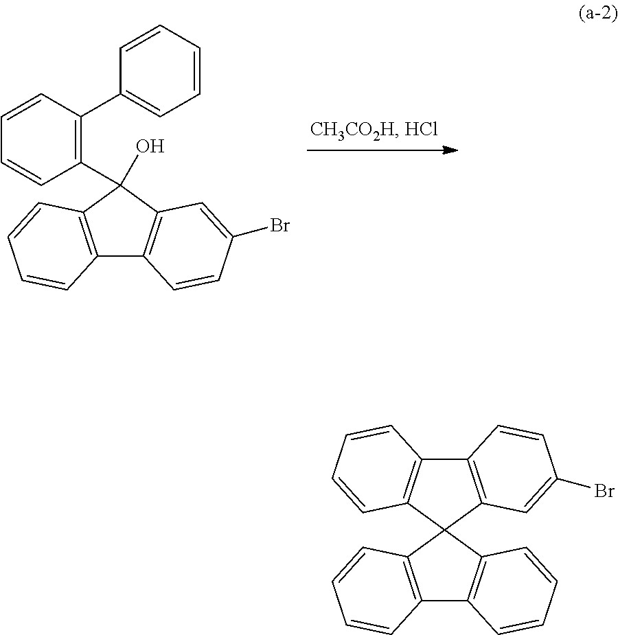
A method of synthesis of DPA will be explained.
25.19 g (0.102 mol) of triphenylamine, 18.05 g (0.102 mol) of N-bromosuccinimide, and 400 mL of ethyl acetate were put in a 1000 mL Erlenmeyer flask, and were stirred for about 12 hours at room temperature in the air. After the reaction was complete, an organic layer was washed twice with a saturated sodium carbonate solution. Then, an aqueous layer was extracted twice with ethyl acetate, combined with the organic layer, and washed with saturated saline solution. The solution was dried with magnesium sulfate, naturally filtered and concentrated, and a colorless solid was obtained. The solid was recrystallized with ethyl acetate and hexane, and 22.01 g of a colorless powdered solid was obtained, in a yield of 66%. It was confirmed that this colorless powdered solid was 4-bromotriphenylamine by a nuclear magnetic resonance method (NMR). The measurement results according to a nuclear magnetic resonance method (NMR) are shown below.
1H NMR of the compound obtained is shown below:
1H NMR (300 MHz, CDCl3) δ ppm: 7.32 (d, 2H, J=8.7 Hz), 7.29-7.23 (m, 4H), 7.08-7.00 (m, 6H), 6.94 (d, 2H, J=8.7 Hz)
Next, a synthesis scheme (b-1) of 4-bromotriphenylamine will be shown.

A dehydrated toluene solution (5 mL) of 4-bromotriphenylamine (559 mg, 6 mmol), Pd(dba)2 (345 mg, 0.6 mmol), and t-BuONa (577 mg, 6 mmol) was degassed. Then, aniline (559 mg, 6 mmol) and P(t-Bu)3. (0.37 mL, 1.8 mmol) were added. The mixture was heated and stirred for 5 hours under a nitrogen atmosphere at 80° C. By thin-film chromatography, it was ascertained that the raw material, 4-bromotriphenylamine, had disappeared. A saturated saline solution was added to complete the reaction, and an aqueous layer was extracted with about 100 ml of ethyl acetate. The organic layer was dried by magnesium sulfate, and filtered. After the filtrate was concentrated, purification was conducted in an ethyl acetate:hexane=1:20 silica gel column, and the target product was obtained as a viscous liquid. By adding hexane to this viscous liquid and applying ultrasonic waves, a cream-colored powder was extracted. This mixture was concentrated, and DPA was obtained in a yield of 42%.
1H NMR of the DPA obtained is shown: 1H NMR (300 MHz, CDCl3) δ ppm: 7.35-6.83 (m, 19H), 5.60 (s, 1H)
Further, the 13C NMR is shown: 13C-NMR (75.5 MHz, DMSO-d6) δ ppm: 147.8, 143.7, 140.2, 139.4, 129.4, 129.3, 127.1, 122.4, 122.0, 119.8, 118.4, 116.8
Next, a synthesis scheme (b-2) of DPA is shown.

A method of synthesis of DPASF will be explained.
2.5 g (6.3 mmol) of 2-bromo-spiro-9,9′-bifluorene, 2.2 g (6.5 mmol) of DPA, 37.6 mg (0.063 mmol) of bis(dibenzylideneacetone)palladium(0), and 2.1 g (21 mmol) of t-butoxysodium were placed in a 100 mL three-necked flask. Nitrogen substitution was carried out, 50 mL of toluene was added, and the mixture was degassed at reduced pressure. 0.1 mL of tri(t-butyl)phosphine (10 wt % hexane solution) was added, and the mixture was stirred for 11 hours at 80° C. After the reaction, filtration was done through Celite. The filtrate was washed 3 times with water and once with a saturated saline solution, and dried with magnesium sulfate. The reaction mixture was naturally filtered, the filtrate was concentrated, and an oily product was obtained. This oily product was purified by silica gel column chromatography (hexane:toluene=7:3), and after recrystallizing from dichloromethane and hexane, the target product of a white powdered solid was obtained, weighing 3.8 g in a yield of 91%. It was confirmed that this white powdered solid was DPASF by a nuclear magnetic resonance method (NMR).
1H NMR of the compound obtained is shown below. Further, a 1H NMR chart is shown in FIG. 10 .
1H NMR (300 MHz, DMSO-d6); δ=7.95 (d, J=7.80 Hz, 2H), 7.90 (d, J=7.80 Hz, 2H), 7.40-7.77 (m, 26H), 6.67 (d, J=7.20 Hz, 2H), 6.55 (d, J=7.20 Hz, 1H), 6.16 (d, J=2.33 Hz, 1H)
A synthesis scheme (c-1) of DPASF is shown below.

Sublimation purification was conducted for 24 hours on 3.75 g of the DPASF obtained, at a pressure of 200 Pa and a temperature of 330° C. 2.82 g was recovered, in a yield of 75%.
Further, the decomposition temperature (Td) of the DPASF was measured with a thereto-gravimetric/differential thermal analyzer (a Seiko Instruments Inc. TG/DTA320), and was found to be 382° C. Thus, it was found that DPASF showed a high Td.
Furthermore, the glass transition temperature (Tg) was measured using a differential scanning calorimeter (a Perkin-Elmer Co., Ltd. Pyris 1 DSC). First, a sample was melted by heating it from 25° C. to 250° C. at 40° C. per minute. Next it was cooled to 25° C., at 40° C. per minute. Next, by raising the temperature to 250° C. at 10° C. per minute, the DSC chart in FIG. 11 was obtained. From this chart, it can be seen that the glass transition temperature (Tg) of DPASF is 107° C. Thus, it was found that DPASF has a high glass transition temperature. In addition, the endothermic peak on the DSC chart of when the sample was first melted was observed. It shows the melting point, which was 223° C.
The absorption spectrum and emission spectrum of DPASF in a thin film state are shown in FIGS. 12 and 13 . It was found that the maximum absorption wavelength of DPASF in a thin film state was 341 nm and the maximum emission wavelength was 434 nm. Using the absorption spectrum data from FIG. 12 , the absorption edge was obtained from a Tauc plot. Using the energy of that absorption edge as an energy gap, the energy gap of DPASF was found to be 3.1 eV. 9,10-diphenylanthracene, which exhibits representative blue emission, has an energy gap of 2.9 eV, so it can be seen that DPASF has an amply large energy gap. Further, the HOMO level in a thin film state was measured with an ambient photoelectron spectroscopy (using a Riken Keiki Co., Ltd. AC-2), and was found to be −53 eV. Using the HOMO level and the energy gap, the LUMO level was found to be −2.2 eV.
Further, the electrochemical stability of DPASF was evaluated using cyclic voltammetry (CV). An electrochemical analyzer (a BAS Inc. ALS model 600A) was used as the measuring device. The solution for the CV measurement was prepared by using dehydrated dimethylformamide (DMF) as a solvent, dissolving a supporting electrolyte of tetra-n-butylammonium perchlorate (n-Bu4NClO4) to a concentration of 100 mM, and dissolving DPASF, the object of measurement, to a concentration of 1 mM. A platinum electrode (a BAS Inc. PTE platinum electrode) was used as a working electrode, another platinum electrode (a BAS Inc. Pt counter electrode (5 cm) for VC-3) was used as an auxiliary electrode, and an Ag/Ag+ electrode (a BAS Inc. RE5 non-aqueous solvent reference electrode) was used as a reference electrode. The scanning speed was set at 0.1 V per second, and a 100 cycle measurement was conducted.
CV measurement results for the oxidation side of DPASF film are shown in FIG. 14 . The graph which shows the measurement results shows a reversible peak, there being almost no change in the cyclic voltammogram even when oxidation is repeated 100 times. This means that DPASF has tolerance to the cycle of oxidation and reduction which follows the oxidation.
In this example, a method of synthesis of 2-[N-(9-phenylcarbazole-3-yl)-N-phenylamino]-spiro-9,9′-bifluorene (abbrev.: PCASF), which is expressed by the Structural Formula 35 in Embodiment Mode 1, will be explained.
PCASF can be synthesized by conducting a coupling reaction with 2-bromo-spiro-9,9′-bifluorene, which is expressed by the Formula 111 below, and 3-(N-phenylamino)-9-phenylcarbazole (abbrev.: PCA), which is expressed by the Formula 113 below, using a metal catalyst. Note that the method of synthesis of 2-bromo-spiro-9,9′-bifluorene was explained in Step 1 of Example 1, so it will not be explained here.

A method of synthesis of PCA will be explained.
First, 24.3 g (100 mmol) of N-phenylcarbazole was dissolved in 600 mL of glacial acetic acid, 17.8 g (100 mmol) of N-bromosuccinimide was slowly added, and the mixture was stirred for about 12 hours at room temperature. This glacial acetic acid solution was added dropwise to 1 L of iced water while stirring. The white solid extracted was washed 3 times with water. This solid was dissolved in 150 mL of diethyl ether, and washed with a saturated sodium hydrogen carbonate solution and water. This organic layer was dried with magnesium sulfate. This was filtered, and the filtrate obtained was concentrated. To the residue obtained was added about 50 mL of methanol, and by irradiation with ultrasonic waves, the residue was dissolved evenly in the solution. By leaving this solution at rest, a white solid was extracted. This white solid was filtered, and by drying the solid, 28.4 g of 3-bromo-9-phenylcarbazole in a white powdered form was obtained (yield rate: 88%).
Next, a synthesis scheme (d-1) of 3-bromo-9-phenylcarbazole will be shown.

Next, under nitrogen, 110 mL of dehydrated xylene and 7.0 g (75 mmol) of aniline were added to a mixture containing 19 g (60 mmol) of 3-bromo-9-phenylcarbazole, 340 mg (0.6 mmol) of bis(dibenzylideneacetone)palladium(0) (abbrev.: Pd(dba)2), 1.6 g (3.0 mmol) of 1,1-bis(diphenylphosphino)ferrocene (abbrev.: DPPF), and 13 g (180 mmol) of sodium-tert-butoxide (abbrev.: tert-BuONa). This mixture was then heated and stirred for 7.5 hours at 90° C. under a nitrogen atmosphere. After the reaction was complete, about 500 mL of toluene warmed to 50° C. was added to this suspension. Then, it was filtered through Florisil, alumina and Celite, and the filtrate obtained was concentrated. To this residue was added hexane-ethyl acetate, and irradiation with ultrasonic waves was conducted. The suspension obtained was filtered, the residue was dried, and 15 g of a cream-colored powder was obtained (yield rate: 75%). It was confirmed that this cream-colored powder was 3-(N-phenylamino)-9-phenylcarbazole (abbrev.: PCA) by a nuclear magnetic resonance method (NMR).
Next, 1H NMR of this compound will be shown. Also, 1H NMR charts are shown in FIGS. 15A and 15B . Note that the chart in FIG. 15B is an enlarged version of the 5 ppm to 9 ppm range in FIG. 15A .
1H NMR (300 Mhz, CDCl3); δ=6.84 (t, J=6.9 Hz, 1H), 6.97 (d, J=7.8 Hz, 2H), 7.20-7.61 (m, 13H), 7.90 (s, 1H), 8.04 (d, 7.8 Hz, 1H).
Next, 1H NMR of this compound will be shown. Also, 1H NMR charts are shown in FIGS. 50A and 50B . Note that the chart in FIG. 50B is an enlarged version of the 6.5 ppm to 8.5 ppm range in FIG. 50A .
1H NMR (300 MHz, DMSO-d6); 5=6.73 (t, J=7.5 Hz, 1H), 7.02 (d, J=8.1 Hz, 2H), 7.16-7.70 (m, 12H), 7.95 (s, 1H), 8.06 (s, 1H), 8.17 (d, J=7.8 Hz).
In addition, the 13C NMR will now be shown. Also, 13C NMR charts are shown in FIGS. 51A and 51B . Note that the chart in FIG. 51B is an enlarged version of the 100 ppm to 150 ppm range in FIG. 51A .
13C NMR (75.5 MHz, DMSO-d6); δ=109.55, 110.30, 110.49, 114.71, 11822, 119.70, 120.14, 120.61, 122.58, 123.35, 126.18, 126.48, 127.37, 129.15, 130.14, 135.71, 136.27, 137.11, 140.41, 145.61.
Next, a synthesis scheme (d-2) of 3-(N-phenylamino)-9-phenylcarbazole is shown.

A method of synthesis of PCASF will be explained.
1.0 g (2.5 mmol) of 2-bromo-spiro-9,9′-bifluorene, 846 mg (2.5 mmol) of 3-(N-phenylamino)-9-phenylcarbazole, 15.0 mg (0.025 mmol) of bis(dibenzylideneacetone)palladium(0), and 1.0 g (10 mmL) of t-butoxy sodium were placed in a 100 mL three-necked flask, and nitrogen substitution was carried out. 10 mL of toluene was added, and the mixture was degassed at reduced pressure. 0.05 mL of tri(t-butyl)phosphine (10 wt % hexane solution) was added, and the mixture was stirred for 3.5 hours at 80° C. After the reaction, the mixture was filtered through Celite. The filtrate was washed 3 times with water and once with a saturated saline solution, and dried with magnesium sulfate. The reaction mixture was naturally filtered, the filtrate was concentrated, and an oily product was obtained. This oily product was purified by silica gel column chromatography (hexane:ethyl acetate=7:3), then recrystallized with dichloromethane and hexane. 1.0 g of a white powdered solid was obtained, in a yield of 63%. It was confirmed that this white powdered solid was PCASF by a nuclear magnetic resonance method (NMR).
Next, 1H NMR of this compound is shown. Also, a 1H NMR chart of PCASF is shown in FIG. 16 .
1H NMR (300 MHz, DMSO-d6); δ=8.04 (d, J=7.21 Hz, 1H), 7.89-7.85 (m, 5H), 7.69-7.50 (m, 5H), 7.43-7.31 (m, 5H), 7.27-7.10 (m, 6H), 7.07-7.01 (m, 2H), 6.95-6.86 (m, 4H), 6.73 (d, J=7.80 Hz, 2H), 6.52 (d, J=7.80 Hz, 1H), 6.31 (d, J=2.4 Hz, 1H)
Next, a synthesis scheme (e-1) of PCASF will be shown.

Sublimation purification was conducted for 24 hours on 551 mg of the PCASF obtained at a pressure of 200 Pa and a temperature of 320° C. 480 mg was recovered, in a yield of 87%.
Further, the decomposition temperature (Td) of the PCASF was measured with a thermo-gravimetric/differential thermal analyzer (a Seiko Instruments Inc. TG/DTA320). It was found to be 371° C. Thus, it was found that PCASF shows a high Td.
Further, the glass transition temperature (Tg) was measured using a differential scanning calorimeter (a PerkinElmer Co., Ltd Pyris 1 DSC). First, a sample was heated from −10° C. to 350° C. by 40° C. per minute, then cooled to −5° C. by 40° C. per minute. Next, by raising the temperature to 350° C. by 10° C. per minute, the DSC chart in FIG. 17 was obtained. From this chart, it can be seen that the glass transition temperature (Tg) of PCASF is 134° C. Thus, it was found that PCASF has a high glass transition temperature. Note that in this measurement, the endothermic peak, which shows the melting point, was not observed.
The absorption spectrum and emission spectrum of PCASF in a thin film state are shown in FIGS. 18 and 19 . It was found that in a thin film state, PCASF had absorption peaks at 312 nm and 359 nm, and the maximum emission wavelength was 437 nm. Using the absorption spectrum data from FIG. 18 , the absorption edge was obtained from a Tauc plot. Using the energy of that absorption edge as an energy gap, the energy gap of PCASF was found to be 3.2 eV. 9,10-diphenylanthracene, which exhibits representative blue emission, has an energy gap of 2.9 eV, so it was found that PCASF has an amply large energy gap. Further, the HOMO level in a thin film state was measured with an ambient photoelectron spectroscopy (using a Riken Keiki Co., Ltd AC-2), and was found to be −5.3 eV. Using the HOMO level and the energy gap, the LUMO level was found to be −2.1 eV.
Further, the electrochemical stability of PCASF was evaluated using cyclic voltammetry (CV). An electrochemical analyzer (a BAS Inc. ALS model 600A) was used as the measuring device. The solution for the CV measurement was prepared by using dehydrated dimethylformamide (DMF) as a solvent, dissolving a supporting electrolyte of tetra-n-butylammonium perchlorate (n-Bu4NClO4) to a concentration of 100 mM, and dissolving PCASF, the object of measurement, to a concentration of 1 mM. A platinum electrode (a BAS Inc. VIE platinum electrode) was used as a working electrode, another platinum electrode (a BAS Inc. Pt counter electrode (5 cm) for VC-3) was used as an auxiliary electrode, and an Ag/Ag+ electrode (a BAS Inc. RE5 non-aqueous solvent reference electrode) was used as a reference electrode. The scanning speed was set at 0.1 V per second, and a 100 cycle measurement was conducted.
Results of the CV measurement for the oxidation side of PCASF film are shown in FIG. 20 . The graph which shows the measurement results shows a reversible peak, there being almost no change in the cyclic voltammogram even when oxidation is repeated 100 times. This means that PCASF has tolerance to the cycle of oxidation and reduction which follows the oxidation, and that it is electrochemically stable.
In this example, a method of synthesis of 2-{N-[4-(N-carbazolyl)phenyl]N-phenylamino}-spiro-9,9′-bifluorene (abbrev.: YGASF), which is expressed by the Structural Formula 66 in Embodiment Mode 1, will be explained.
YGASF can be synthesized by conducting a coupling reaction with 2-bromo-spiro-9,9′-bifluorene, which is expressed by Formula 111 below, and 9-[4-(N-phenylamino)phenyl]carbazole (abbrev.: YGA), which is expressed by Formula 114 below, using a metal catalyst. Note that the method of synthesis of 2-bromo-spiro-9,9′-bifluorene was explained in Step 1 of Example 1, so it will not be explained here.

A method of synthesis of YGA will be explained.
56.3 g (0.24 mol) of 1,4-dibromobenzene, 31.3 g (0.18 mol) of carbazole, 4.6 g (0.024 mol) of copper iodide, 66.3 g (0.48 mol) of potassium carbonate, and 2.1 g (0.008 mol) of 18-crown-6-ether were placed in a 300 mL three-necked flask, and nitrogen substitution was carried out. 8 mL of DMPU was added, and the mixture was stirred for 6 hours at 180° C. After cooling the reaction mixture to room temperature, the precipitate was removed by suction filtration. The filtrate was washed with dilute hydrochloric acid, a saturated sodium hydrogen carbonate solution, and a saturated saline solution, in that order, then dried with magnesium sulfate. After drying, the reaction mixture was filtered naturally, the filtrate was concentrated, and the oily substance obtained was purified by silica gel column chromatography (hexane:ethyl acetate=9:1). After recrystallization from chloroform and hexane, 20.7 g of light brown plate-shaped crystals were obtained, in a yield of 35%. By a nuclear magnetic resonance method (NMR), it was ascertained that these light brown plate-shaped crystals were N-(4-bromophenyl)carbazole.
Next, 1H NMR of the compound obtained will be shown.
1H NMR (300M Hz, DMSO-d6) δ ppm: 8.14 (d, J=7.8 Hz, 2H), 7.73 (d, J=8.7 Hz, 2H), 7.46 (d, J=8.4 Hz, 2H), 7.42-7.26 (m, 6H)
A synthesis scheme (f-1) of N-(4-bromophenyl)carbazole will be shown next.

5.4 g (17.0 mmol) of N-(4-bromophenyl)carbazole, 1.8 mL (20.0 mmol) of aniline, 100 mg (0.17 mmol) of bis(dibenzylideneacetone)palladium(0) (abbrev.: Pd(dba)2), and 3.9 g (40 mmol) of sodium-tert-butoxide (abbrev.: tert-BuONa) were put in a 200 mL three-necked flask, and nitrogen substitution was conducted. 0.1 mL of tri-tert-butylphosphine (abbrev.: P(tert-Bu)3) and 50 mL of toluene were added, and the mixture was stirred for 6 hours at 80° C. The reaction mixture was filtered through Florisil, Celite and alumina. The filtrate was washed with water and a saturated saline solution, then dried with magnesium sulfate. The reaction mixture was filtered naturally. The filtrate was concentrated, and the oily product obtained was purified by silica gel column chromatography (hexane:ethyl acetate=9:1), giving 4.1 g of the target product, in a yield of 73%. It was confirmed that this compound was YGA by a nuclear magnetic resonance method (NMR).
1H NMR of the compound which was obtained will be shown next. Also, 1H NMR charts are shown in FIGS. 21A and 21B . Note that the chart in FIG. 21B shows an enlarged version of the 6.7 ppm to 8.6 ppm range of FIG. 21A .
1H NMR (300 MHz, DMSO-d6) δ ppm: 8.47 (s, 1H), 8.22 (d, J=7.8 Hz, 2H), 7.44-7.16 (m, 14H), 6.92-6.87 (m, 1H)
Next, a synthesis scheme (f-2) of YGA is shown.

Synthesis of YGASF.
2.0 g (51 mmol) of 2-bromo-spiro-9,9′-bifluorene, 1.7 mg (5.1 mmol) of YGA, 30.4 mg (0.05 mmol) of bis(dibenzylideneacetone)palladium(0), and 2.0 g (21 mmol) of t-butoxysodium were put in a 100 mL three-necked flask, and nitrogen substitution was carried out. 30 mL of toluene was added, and the mixture was degassed at reduced pressure. 0.1 mL of tri(t-butyl)phosphine (10 wt % hexane solution) was added, and the mixture was stirred for 6 hours at 80° C. After the reaction, the mixture was filtered through Celite. The filtrate was washed 3 times with water and once with a saturated saline solution, and dried with magnesium sulfate. The reaction mixture was filtered naturally, the filtrate was concentrated, and an oily product was obtained. This oily product was purified by silica gel column chromatography (hexane:toluene=7:3). After recrystallization from chloroform and hexane, a white powdered solid was obtained, weighing 2.9 g in a yield of 88%. It was confirmed that this white powdered solid was YGASF by a nuclear magnetic resonance method (NMR).
1H NMR of the compound which was obtained is shown below. In addition, a NMR chart is shown in FIG. 22 .
1H NMR (300 MHz, DMSO-d6); δ=8.19 (d, J=7.80 Hz, 2H), 7.97-7.91 (m, 4H), 7.43-7.01 (m, 22H), 6.71 (d, J=7.80 Hz, 2H), 6.71 (d, J=7.80 Hz, 2H), 6.58 (d, J=6.9 Hz, 1H) 6.32 (d, J=2.10 Hz, 1H)
Next, a synthesis scheme (g-1) of YGASF will be shown.

Sublimation purification was conducted for 24 hours on 230 g of the YGASF obtained, at a pressure of 6.7 Pa and a temperature of 300° C. 2.4 g was recovered, in a yield of 96%.
Further, the decomposition temperature (Td) of the YGASF was measured with a thermo-gravimetric/differential thermal analyzer (a Seiko Instruments Inc. TG/DTA320). It was found to be 371° C. Thus, it was found that YGASF shows a high Td.
Further, the glass transition temperature (Tg) was measured using a differential scanning calorimeter (a Perkin Elmer Co., Ltd Pyris 1 DSC). First, a sample was heated from −10° C. to 320° C. by 40° C. per minute and melted. Then it was cooled to −10° C. by 40° C. per minute. Next, by raising the temperature to 320° C. by 10° C. per minute, the DSC chart in FIG. 23 was obtained. From this chart, it was found that the glass transition temperature (Tg) of YGASF was 129° C. Thus, it was found that YGASF has a high glass transition temperature. Further, the endothermic peak on the DSC chart of when the sample was first melted was observed. It shows the melting point, which was 296° C.
The absorption spectrum and emission spectrum of YGASF in a thin film state are shown in FIGS. 24 and 25 . It was found that in a thin film state, YGASF had a maximum absorption wavelength of 242 nm, and a maximum emission wavelength of 406 nm. Using the absorption spectrum data from FIG. 24 , the absorption edge was obtained from a Tauc plot. Using the energy of that absorption edge as an energy gap, the energy gap of YGASF was found to be 3.3 eV. 9,10-diphenylanthracene, which exhibits representative blue emission, has an energy gap of 2.9 eV, so it was found that YGASF has an amply large energy gap. Further, the HOMO level in a thin film state was measured with an ambient photoelectron spectroscopy (using a Riken Keiki Co., Ltd AC-2), and was found to be −5.3 eV. The LUMO level was obtained using the HOMO level and the energy gap, and was −2.0 eV.
Further, the electrochemical stability of YGASF was evaluated using cyclic voltammetry (CV). An electrochemical analyzer (a BAS Inc. ALS model 600A) was used as the measuring device. A solution for the CV measurement was prepared by using dehydrated dimethylformamide (DMF) as a solvent, dissolving a supporting electrolyte of tetra-n-butylammonium perchlorate (n-Bu4NClO4) to a concentration of 100 mM, and dissolving YGASF, the object of measurement, to a concentration of 1 mM. A platinum electrode (a BAS Inc. PTE platinum electrode) was used as a working electrode, another platinum electrode (a BAS Inc. Pt counter electrode (5 cm) for VC-3) was used as an auxiliary electrode, and an Ag/Ag+ electrode (a BAS Inc. RE5 non-aqueous solvents reference electrode) was used as a reference electrode. The scanning speed was set at 0.1 V per second, and a 100 cycle measurement was conducted.
CV measurement results for the oxidation side of YGASF film are shown in FIG. 26 . The graph showing the measurement results shows a reversible peak, there being almost no change in the cyclic voltammogram even when oxidation is repeated 100 times. This means that YGASF has tolerance to the cycle of oxidation and reduction which follows the oxidation, and that it is electrochemically stable.
In this example, a method of synthesis of 2,7-bis[N-(diphenylaminophenyl)-N-phenylamino]-spiro-9,9′-bifluorene (abbrev.: DPA2SF), which is expressed by Structural Formula 26 in Embodiment Mode 1, will be explained.
DPA2SF can be synthesized by conducting a coupling reaction with 2,7-dibromo-spiro-9,9′-bifluorene, which is expressed by Formula 115 below, and DPA, which is expressed by Formula 112 below, using a metal catalyst. Note that the method of synthesis of DPA was explained in Step 2 of Example 1, so it will not be explained here. Step 2 of Example 1 should be referred to.

7.2 g (40.0 mmol) of 9-fluorenone, 14.2 g (44.0 mmol) of iodobenzene diacetate, 60 mL of glacial acetic acid, and 60 mL of acetic anhydride were put in a 300 mL conical flask. In addition, 2.1 mL (41.2 mmol) of bromine and one drop of sulfuric acid were added, and the mixture was stirred for 1 hour at room temperature. After the reaction, the precipitates were filtered. The precipitates were recrystallized with ethanol, and 9.2 g of 2,7-dibromo-9-fluorenone, a yellow solid, was obtained in a yield of 68%.
A synthesis scheme (h-1) of 2,7-dibromo-9-fluorenone is shown below.

1.26 g (51.9 mmol) of magnesium was put in a 50 mL three-necked flask, and was stirred while a vacuum was drawn by a rotary pump. After returning the air to atmospheric pressure, 5 mL of diethyl ether and 1 drop of dibromoethane were added. Further, 8.3 mL (50 mmol) of 2-bromobiphenyl dissolved in 15 mL of diethyl ether was added dropwise, and the mixture was refluxed for 3 hours at 50° C. to make a Grignard reagent.
A manufacturing scheme (h-2) of the Grignard reagent is shown below.

15.2 g (45 mmol) of 2,7-dibromo-9-fluorenone was put in a 100 mL three-necked flask, and nitrogen substitution was conducted. 40 mL of diethyl ether was added. The Grignard reagent above was transferred into a dropping funnel by a cannula so as not to expose it to the atmosphere, and was added dropwise into the mixture. The mixture was refluxed at 50° C. After the reaction, the solution was washed with water. Then the aqueous layer was extracted with ethyl acetate and combined with the organic layer. The layers were washed with a saturated saline solution, then dried with magnesium sulfate. Filtration and concentration were carried out, and 22 g of 9-(biphenyl-2-yl)-2,7-dibromo-9-fluorenol was obtained as a white solid, in a yield of 90%.
A synthesis scheme (h-3) of 9-(biphenyl-2-yl)-2,7-dibromo-9-fluorenol is shown below.

22 g (45.0 mmol) of 9-biphenyl-2-yl-2,7-dibromo-9-fluorenol, and 100 mL of glacial acetic acid were placed in a 300 mL three-necked flask, several drops of concentrated hydrochloric acid were added, and the mixture was refluxed. After the reaction, the precipitates were filtered. The precipitate was recrystallized with ethanol, and 12.3 g of 2,7-dibromo-spiro-9,9′-bifluorene was obtained as a white solid, in a yield of 57%.
A synthesis scheme (h-4) of 2,7-dibromo-9,9′-spiro-bifluorene is shown below.

Synthesis of DPA2SF.
5.0 g (10.6 mmol) of 2,7-dibromo-spiro-9,9′-bifluorene, 7.4 g (21.0 mmol) of DPA, 63 mg (0.1 mmol) of bis(dibenzylideneacetone)palladium(0), and 3.6 g (37 mmol) of t-butoxysodium were placed in a 300 mL three-necked flask, and nitrogen substitution was conducted. 100 mL of toluene was added to the mixture, and the mixture was degassed at reduced pressure. 0.05 mL of tri(t-butyl)phosphine (10 wt % hexane solution) was added, and the mixture was stirred for 6 hours at 80° C. After the reaction, the mixture was filtered through Celite. The filtrate was washed 3 times with water and once with a saturated saline solution, then dried with magnesium sulfate. The reaction mixture was naturally filtered, and the filtrate was concentrated to obtain an oily product. This oily product was purified by silica gel column chromatography (hexane:ethyl acetate=7:3), and recrystallized with chloroform and ethanol, giving 6.0 g of a pale yellow powdered solid in a yield of 57%. It was confirmed that this pale yellow powdered solid was DPA2SF by a nuclear magnetic resonance method (NMR).
1H NMR of the compound obtained is shown below. Also, a 1H NMR chart is shown in FIG. 27 .
1H NMR (300 MHz, DMSO-d6); δ=7.84 (d, J=7.21 Hz, 2H), 7.77 (d, J=7.80 Hz, 2H), 7.32-7.79 (m, 40H), 6.73 (d, J=7.80 Hz, 2H), 6.16 (d, J=2.10 Hz, 2H)
A synthesis scheme (i-1) of DPA2SF is shown below.

Sublimation purification was conducted on 2.0 g of the DPA2SF for 24 hours at a pressure of 6.7 Pa and a temperature of 350° C. 1.3 g was recovered, in a yield of 66%.
Further, the decomposition temperature (Td) of the DPA2SF was measured with a thermo-gravimetric/differential thermal analyzer (a Seiko Instruments Inc. TG/DTA320), and was found to be 436° C. Thus, it was found that DPA2SF shows excellent heat resistance.
In addition, the glass transition temperature (Tg) was measured using a differential scanning calorimeter (a Perkin-Elmer Co., Ltd Pyris 1 DSC). First, a sample was heated from 25° C. to 450° C. at 40° C. per minute. Next, it was cooled to 25° C., at 40° C. per minute. Then, by raising the temperature to 450° C. at 10° C. per minute, the DSC chart in FIG. 28 was obtained. From this chart, it was found that the glass transition temperature (Tg) of DPA2SF is 132° C. Thus, it was found that DPA2SF has a high glass transition temperature. Note that in this measurement, the endothermic peak, which shows the melting point, was not observed.
The absorption spectrum and emission spectrum of DPA2SF in a thin film state are shown in FIGS. 29 and 30 . It was found that in a thin film state, DPA2SF had a maximum absorption wavelength of 390 nm, and a maximum emission wavelength of 433 nm. Using the absorption spectrum data from FIG. 29 , the absorption edge was obtained from a Tauc plot. Using the energy of that absorption edge as an energy gap, the energy gap of DPA2SF was found to be 3.0 eV. Since 9,10-diphenylanthracene, which exhibits representative blue emission, has an energy gap of 2.9 eV, it can be seen that DPA2SF has an amply large energy gap. Further, the HOMO level in a thin film state was measured by an ambient photoelectron spectroscopy (using a Riken Keiki Co., Ltd AC-2), and was found to be −5.1 eV. Using the HOMO level and the energy gap, the LUMO level was found to be −2.1 eV.
Further, the electrochemical stability of DPA2SF was evaluated using cyclic voltammetry (CV). An electrochemical analyzer (a BAS Inc. ALS model 600A) was used as the measuring device. A solution for the CV measurement was prepared by using dehydrated dimethylformamide (DMF) as a solvent, dissolving a supporting electrolyte of tetra-n-butylammonium perchlorate (n-Bu4NClO4) to a concentration of 100 mM, and dissolving DPA2SF, the object of measurement, to a concentration of 1 mM. A platinum electrode (a BAS Inc. PTE platinum electrode) was used as a working electrode, another platinum electrode (a BAS Inc. Pt counter electrode (5 cm) for VC-3) was used as an auxiliary electrode, and an Ag/Ag+ electrode (a BAS Inc. RE5 non-aqueous solvent reference electrode) was used as a reference electrode. The scanning speed was set at 0.1 V per second, and a 100 cycle measurement was conducted.
CV measurement results for the oxidation side of DPA2SF film are shown in FIG. 31 . The graph which shows the measurement results shows a reversible peak, there being almost no change in the cyclic voltammogram even when oxidation is repeated 100 times. This means that DPA2SF has tolerance to the cycle of oxidation and reduction which follows the oxidation, and that it is electrochemically stable.
In this example, a manufacturing method of a light-emitting element using DPASF for a hole transporting layer will be explained. Characteristics of such a light-emitting element will also be explained.
A light-emitting element was formed over a glass substrate. Over the glass substrate, a 110 nm ITSO film was formed as a first electrode. The aforementioned ITSO film was formed by a sputtering method. Note that in the present invention, the shape of the first electrode was set at 2 mm×2 mm. Next, as pre-treatment for forming a light-emitting element over the first electrode, a surface of the substrate was washed with a porous resin (typically, a resin made of PVA (polyvinyl alcohol), nylon or the like), heat treatment was carried out for 1 hour at 200° C., and UV ozone treatment was conducted for 370 seconds.
Next, a 40 nm co-evaporation film of NPB and molybdenum oxide (MoOx) was formed as a hole injecting layer (NPB:MoOx=4:2). Then, a 20 nm film of DPASF was formed as a hole transporting layer. Over this stack of films, a 40 nm co-evaporation film of t-BuDNA and 1,1,4,4-tetraphenyl-1,3-butadiene (TBP) was formed as a light-emitting layer. The weight ratio of t-BuDNA and TBP was set at 1:0.01. In addition, a 20 nm film of Alq was formed as an electron transporting layer, and a 1 nm film of calcium fluoride (CaF2) was formed as an electron injecting layer. Lastly, a 200 nm film of Al was formed as a second electrode, thereby completing the element. Note that the layers from the hole injecting layer to the second electrode were all formed by a vacuum deposition method using heat resistance.
Current density-luminance characteristics, luminance-current efficiency characteristics and voltage-luminance characteristics of the element manufactured are shown in FIG. 32 , FIG. 33 and FIG. 34 , respectively. It can be seen that the light-emitting element using a spirofluorene derivative of the present invention exhibits excellent characteristics. In addition, since the light-emitting element manufactured uses the spirofluorene derivative of the present invention, which has a high Tg, it has high heat resistance.
In this example, a manufacturing method of a light-emitting element using YGASF for a hole transporting layer, and characteristics of such a light-emitting element, will be explained.
A light-emitting element was formed over a glass substrate. Over the glass substrate, a 110 nm film of ITSO was formed as a first electrode. This ITSO film was formed by a sputtering method. Note that in the present invention, the first electrode had a shape of 2 mm×2 mm. Next, as pretreatment for forming a light-emitting element over the first electrode, a surface of the substrate was washed with a porous resin (typically, a resin made of PVA (polyvinyl alcohol), nylon, or the like), heat treatment was conducted for 1 hour at 200° C., and UV ozone treatment was conducted for 370 seconds.
Next, a 40 nm co-evaporation film of NPB and molybdenum oxide (MoOx) was formed as a hole injecting layer (NPB:MoOx=4:2). Then, a 20 nm film of YGASF was formed as a hole transporting layer. Over this stack of films, a 40 nm co-evaporation film of t-BuDNA and 2,5,8,11-tetra(tert-butyl)perylene (TBP) was formed as a light-emitting layer. The weight ratio of t-BuDNA and TBP was set at 1:0.01. In addition, a 20 nm film of Alq was formed as an electron transporting layer, and a 1 nm film of calcium fluoride (CaF2) was formed as an electron injecting layer. Lastly, a 200 nm film of Al was formed as a second electrode, and the element was thereby completed. Note that the films from the hole injecting layer to the second electrode were all formed by a vacuum deposition method using heat resistance.
Current density-luminance characteristics, luminance-current efficiency characteristics and voltage-luminance characteristics of the element manufactured are shown in FIG. 35 , FIG. 36 and FIG. 37 , respectively. It can be seen that a light-emitting element using the spirofluorene derivative of the present invention exhibits excellent characteristics. Further, in particular, the element of the present example using YGASF for a hole transporting layer has excellent voltage-luminance characteristics. Furthermore, since the light-emitting element manufactured uses the spirofluorene derivative of the present invention, which has a high glass transition temperature (Tg), it has high heat resistance.
In this example, a manufacturing method of a light-emitting element using PCASF for a hole transporting layer, and characteristics of such a light-emitting element, will be explained.
A light-emitting element was formed over a glass substrate. Over the glass substrate, a film of ITSO was formed with a thickness of 110 nm as a first electrode. The ITSO film was formed by a sputtering method. Note that in the present invention, the first electrode had a shape of 2 mm×2 mm. Next, as pretreatment for forming a light-emitting element over the first electrode, a surface of the substrate was washed by a porous resin (typically, a resin made of PVA (polyvinyl alcohol), nylon, or the like), heat treatment was conducted for 1 hour at 200° C., and UV ozone treatment was conducted for 370 seconds.
Next, a 40 nm co-evaporation film of NPB and molybdenum oxide (MoOx) was formed as a hole injecting layer (NPB:MoOx=4:2). Then, a 20 nm film of PCASF was formed as a hole transporting layer. Over this stack of films, a 40 nm co-evaporation film of t-BuDNA and TBP was formed as a light-emitting layer. The weight ratio of t-BuDNA and TBP was set at 1:0.01. In addition, a 20 nm film of Alq was formed as an electron transporting layer, and a 1 nm film of calcium fluoride (CaF2) was formed as an electron injecting layer. Lastly, a 200 nm film of Al was formed as a second electrode, completing the element. Note that the films from the hole injecting layer to the second electrode were all formed by a vacuum deposition method using heat resistance.
The current density-luminance characteristics, luminance-current efficiency characteristics and voltage-luminance characteristics of the element manufactured are shown in FIG. 38 , FIG. 39 and FIG. 40 , respectively. It can be seen that a light-emitting element using the spirofluorene derivative of the present invention exhibits excellent characteristics. Further, since the light-emitting element manufactured uses the spirofluorene derivative of the present invention, which has a high glass transition temperature (Tg), it has high heat resistance.
In this example, a composite material containing DPASF and molybdenum oxide (MoOx) and a manufacturing method of a light-emitting element using the composite material for a hole injecting layer will be explained. Also, characteristics of the light emitting element will be explained.
An absorption spectrum of a thin film of DPASF and an absorption spectrum of a thin film of the composite material containing DPASF and molybdenum oxide are shown in FIG. 41 . Note that in FIG. 41 , the thick line shows the spectrum of the composite material, and the thin line shows the spectrum of DPASF only. From FIG. 41 , it can be seen that the shape of the DPASF-only absorption spectrum is different from the shape of the absorption spectrum of the composite material. It is thought that the difference in the absorption spectrums is not something that can also be explained from an absorption spectrum of molybdenum oxide only. It is thought that the difference showed due to DPASF interacting with molybdenum oxide. It is thought that the interaction is the giving and receiving of electrons between DPASF and molybdenum oxide. As a result of the giving and receiving of electrons, the carrier density inside the composite material increases, and thereby, beneficial effects can be obtained. For example, a hole injecting property is improved. Also, even when a film is thickened, a rise in driving voltage is small.
A light-emitting element was formed over a glass substrate. Over the glass substrate, a 110 nm film of ITSO was formed as a first electrode. The ITSO was formed by a sputtering method. Note that in the present invention, the shape of the first electrode was 2 mm×2 mm. Next, as pretreatment for forming a light-emitting element over the first electrode, a surface of the substrate was washed with a porous resin (typically a resin made of PVA (polyvinyl alcohol), nylon, or the like), heat treatment was conducted for 1 hour at 200° C., and UV ozone treatment was conducted for 370 seconds.
Next, a 50 nm co-evaporation film of DPASF and molybdenum oxide (MoOx) was formed as a hole injecting layer (DPASF:MoOx=4:1). Then, a 10 nm film of NPB was formed as a hole transporting layer. Over this stack of films, a 40 nm co-evaporation film of Alq3 and coumarin 6 was formed as a light-emitting layer. The weight ratio of Alq3 and coumarin 6 was set at 1:0.01. In addition, a 10 nm film of Alq was formed as an electron transporting layer, and a 30 nm co-evaporation film of Alq3 and lithium was formed as an electron injecting layer. The weight ratio of Alq3 and lithium was set at 1:0.01. Lastly, a 200 nm film of Al was formed as a second electrode, thereby completing the element. Note that the films from the hole injecting layer to the second electrode were all formed by a vacuum deposition method using heat resistance. As a raw material for molybdenum oxide, molybdenum oxide (VI) was used.
Current density-luminance characteristics, luminance-current efficiency characteristics and voltage-luminance characteristics of the element manufactured are shown in FIG. 42 , FIG. 43 and FIG. 44 , respectively. It can be seen that a light-emitting element using a composite material containing a spirofluorene derivative of the present invention and a metal oxide exhibits excellent characteristics. Further, since the light-emitting element manufactured uses the spirofluorene derivative of the present invention, which has a high glass transition temperature (Tg), it has high heat resistance.
In this example, a composite material containing DPA2SF and molybdenum oxide, and a manufacturing method of a light-emitting element using the composite material as a hole injecting layer, will be explained. Characteristics of the light emitting element will also be explained.
An absorption spectrum of DPA2SF and an absorption spectrum of the composite material containing DPA2SF and molybdenum oxide (MoOx) are shown in FIG. 45 . Note that in FIG. 45 , the thick line shows the spectrum of the composite material, and the thin line shows the spectrum of DPA2SF only. From FIG. 45 , it can be seen that the shape of the DPA2SF-only absorption spectrum is different from the shape of the absorption spectrum of the composite material. It is thought that the difference in the absorption spectrums is not something that can also be explained from an absorption spectrum of molybdenum oxide only. It is thought that the difference showed due to DPA2SF interacting with molybdenum oxide. It is thought that the interaction is the giving and receiving of electrons between DPA2SF and molybdenum oxide. As a result of the giving and receiving of electrons, the carrier density inside the composite material increases, so beneficial effects can be obtained. For example, a hole injecting property can be improved. Also, even when a film thickens, a rise in driving voltage is small.
A light-emitting element was formed over a glass substrate. Over the glass substrate, a 110 nm film of ITSO was formed as a first electrode. The ITSO was formed by a sputtering method. Note that in the present invention, the shape of the first electrode was 2 mm×2 mm. Next, as pretreatment for forming a light-emitting element over the first electrode, a surface of the substrate was washed with a porous resin (typically a resin made of PVA (polyvinyl alcohol), nylon, or the like), heat treatment was conducted for 1 hour at 200° C., and UV ozone treatment was conducted for 370 seconds.
Next, a 50 nm co-evaporation film of DPA2SF and molybdenum oxide (MoOx) was formed as a hole injecting layer (DPA2SF:MoOx=4:1). Then, a 10 nm film of NPB was formed as a hole transporting layer. Over this stack of films, a 40 nm co-evaporation film of Alq3 and coumarin 6 was formed as a light-emitting layer. The weight ratio of Alq3 and coumarin 6 was set at 1:0.01. In addition, a 10 nm film of Alq was formed as an electron transporting layer, and a 30 nm co-evaporation film of Alq3 and lithium was formed as an electron injecting layer. The weight ratio of Alq3 and lithium was set at 1:0.01. Lastly, a 200 nm film of Al was formed as a second electrode, thereby completing the element. Note that the films from the hole injecting layer to the second electrode were all formed by a vacuum deposition method using heat resistance.
Current density-luminance characteristics, luminance-current efficiency characteristics and voltage-luminance characteristics of the element manufactured are shown in FIG. 46 , FIG. 47 and FIG. 48 , respectively. It can be seen that a light-emitting element using a composite material containing a spirofluorene derivative of the present invention and a metal oxide exhibits excellent characteristics. Further, since the light-emitting element manufactured uses the spirofluorene derivative of the present invention, which has a high glass transition temperature (Tg), it has high heat resistance.
In this example, a manufacturing method of a light-emitting element having a hole transporting layer formed of two layers, a layer of YGASF and a layer of NPB, is explained. Characteristics of such a light-emitting element are also explained.
A manufacturing method of a light-emitting element of this example will be explained using FIG. 1 . A light-emitting element was formed over a glass substrate. Over the glass substrate, a 110 nm film of ITSO was formed as a first electrode 101. The ITSO was formed by a sputtering method, and the shape of the first electrode 101 was made 2 mm×2 mm by etching. Next, as pretreatment for forming a light-emitting element over the first electrode 101, a surface of the substrate was washed with a porous resin (typically a resin made of PVA (polyvinyl alcohol), nylon, or the like), heat treatment was conducted for 1 hour at 200° C., and UV ozone treatment was conducted for 370 seconds.
Next, a formation method of the organic layer 102 will be explained. First, a 50 nm co-evaporation film of NPB and molybdenum oxide was formed as a hole injecting layer. The film was formed with the mass ratio of NPB to molybdenum oxide set at 4:1. Next, a 10 nm film of NPB was formed as a first hole transporting layer. Over this stack of films, a 2 nm film of YGASF was formed as a second hole transporting layer, and a film of 9-[4-(N-carbazolyl)]phenyl-10-phenylanthracene (abbrev.: CzPA) and 9-(4-{N-[4-(9-carbazolyl)phenyl]-N-phenylamino}phenyl)-10-phenylanthracene (abbrev.: YGAPA) was formed as a light-emitting layer, with the mass ratio of CzPA to YGAPA at 1:0.04. In this film, CzPA functions as a host material, and YGAPA functions as a light-emission center material. The light-emitting layer was formed to be 30 nm thick. In addition, a 30 nm film of Alq3 was formed as an electron transporting layer, and a 1 nm film of lithium fluoride was formed as an electron injecting layer. Next, a 200 nm film of Al was formed as a second electrode 103, completing the element. Finally, the element was sealed under a nitrogen atmosphere so that it would not be exposed to the atmosphere (the element of Example 10). Note that the films from the hole injecting layer to the second electrode were all formed by a vacuum deposition method using heat resistance.
As comparative examples, an element (Comparative Example 1 Element) having the same structure as the above element and having a second hole transporting layer formed of 4,4′-bis[N-(9,9-dimethylfluorene-2-yl)-N-phenylamino]biphenyl (abbrev.: DFLDPBi), and an element (Comparative Example 2 Element) having a first hole transporting layer only, and no second hole transporting layer, were manufactured.
Table 1 shows current efficiency, power efficiency, and the like for the element of Example 10, Comparative Example 1 Element, and Comparative Example 2 Element.
| TABLE 1 | ||||
| Energy Gap of 2nd | Current | Power | ||
| Hole Transporting | Efficiency | Efficiency | ||
| Layer (eV) | (cd/A) | (lm/W) | ||
| Embidiment 9 | 3.17 | 4.16 | 2.33 |
| Example 1 | 2.97 | 1.74 | 0.78 |
| Example 2 | — | 1.98 | 1.04 |
| ※ about 1000 cd | |||
From Table 1 it can be seen that the element of Example 10 shows excellent values for both current efficiency and power efficiency, compared to the elements of the comparative examples.
It is thought that this is due to improvement in light-emitting efficiency. In the element of Example 10, the energy gap of the host material CzPA is 3.0 eV. This is close to the energy gap of the first hole transporting layer, NPB, which is 3.1 eV. By providing YGASF, which has a large energy gap of 3.3 eV, between CzPA and NPB, the transfer of excitation energy from the host CzPA to NPB is suppressed. Therefore, light-emitting efficiency is improved. As for Comparative Example 1 Element, which used DFLDPBi for a second hole transporting layer, it is thought that there were no improvement in its characteristics because DFLDPBi has an energy gap of 3.1 eV, which is the same as the energy gap of the first hole transporting layer, NPB.
Thus, the light-emitting element of this embodiment mode has high light-emitting efficiency. Further, due to improvement in light-emitting efficiency, the same luminance can be obtained with less current than when using conventional elements. Therefore, deterioration of a light-emitting element is suppressed, and the light-emitting element has better reliability. Furthermore, since power efficiency is also improved, the light-emitting element has low power consumption.
Note that in the structure of this embodiment mode, a spirofluorene derivative described in Embodiment Mode 1 may be used for the second hole transporting layer. However, it is necessary to select a material of the first hole transporting layer and the host material appropriately so that the energy gap of the second hole transporting layer is larger than that of the first hole transporting layer, and equal to or larger than that of the host material. Further, the thickness of the second hole transporting layer is 0.1 nm or more and less than 5 nm. Preferably it is 0.5 nm to 3 nm, more preferably, 1 nm to 2 nm.
Since the YGAPA and CzPA used in Example 10 are novel materials, synthesis methods thereof will be described below.
First, a method of synthesis of YGAPA, which is expressed by Structural Formula 116 below, will be explained.

5.4 g (21.1 mmol) of 9-bromoanthracene, 2.6 g (21.1 mmol) of phenylbromic acid, 60 mg (0.21 mmol) of Pd(OAc)2, 10 ml (20 mmol) of a 2 mol/l potassium carbonate (K2CO3) aqueous solution, 263 mg (0.84 mmol) of tri(orthotolyl)phosphine (P(o-tolyl)3), and 20 ml of 1,2-dimethoxyethane (abbrev.: DME) were mixed, and stirred for 9 hours at 80° C. After the reaction, the solid extracted was recovered by suction filtration. Then it was dissolved in toluene and filtered through Florisil, Celite, and alumina. After the filtrate was washed by water and a saturated saline solution, it was dried with magnesium sulfate. After natural filtration, the filtrate was concentrated, and the target substance of 9-phenylanthracene was obtained in a light brown solid form, weighing 21.5 g in a yield of 85% (synthesis scheme (j-3)).

6.0 g (23.7 mmol) of 9-phenylanthracene was dissolved in 80 ml of carbon tetrachloride. A solution of 3.80 g (21.1 mmol) of bromine dissolved in 10 ml of carbon tetrachloride was delivered dropwise into that reaction solution by a dropping funnel. After the dropping was complete, the mixture was stirred for 1 hour at room temperature. After the reaction, a sodium thiosulfate solution was added to stop the reaction. An organic layer was washed with a NaOH solution and a saturated saline solution, and dried with magnesium sulfate. After natural filtration, concentration and dissolving in toluene were conducted. Then, filtration was done through Florisil, Celite and alumina. The filtrate was concentrated, then recrystallized with dichloromethane and hexane. The target substance, 9-bromo-10-phenylanthracene, was obtained in the form of a pale yellow solid, weighing 7.0 g in a yield of 89% (synthesis scheme (j-4)).

3.33 g (10 mmol) of 9-bromo-10-phenylanthracene was dissolved in 80 ml of tetrahydrofuran (abbrev.: THF). After bringing the temperature to −78° C., 7.5 ml (12.0 mmol) of n-BuLi (1.6M) was added to the reaction solution dropwise with a dropping funnel, and the mixture was stirred for 1 hour. A solution of 5 g (20.0 mmol) of iodine dissolved in 20 ml of THF was added dropwise, and the mixture was stirred for another 2 hours at −78° C. After the reaction, a sodium thiosulfate solution was added and the reaction was stopped. The organic layer was washed with a sodium thiosulfate solution and a saturated saline solution, and dried with magnesium sulfate. After natural filtration, the filtrate was concentrated, and the solid obtained was recrystallized with ethanol. The target substance of 9-iodo-10-phenylanthracene was obtained as a pale yellow solid, weighing 3.1 g in a yield of 83% (synthesis scheme (j-5)).

1.0 g (2.63 mmol) of 9-iodo-10-phenylanthracene, 542 mg (2.70 mmol) of p-bromophenylboronic acid, 46 mg (0.03 mmol) of Pd(PPh3)4, 3 ml (6 mmol) of 2 mol/L potassium carbonate (K2CO3) solution, and 10 ml of toluene were stirred for 9 hours at 80° C. After the reaction, toluene was added, and the mixture was filtered through Florisil, Celite, and alumina. The filtrate was washed with water and a saturated saline solution, then dried with magnesium sulfate. After natural filtration, the filtrate was concentrated, and recrystallized with chloroform and hexane. The target substance of 9-(4-bromophenyl)-10-phenylanthracene was obtained as a light brown solid, weighing 562 mg in a yield of 45% (synthesis scheme (j-6)).

409 mg (1.0 mmol) of 9-(4-bromophenyl)-10-phenylanthracene, 339 mg (1.0 mmol) of YGA (the manufacturing method of which was shown in Step 1 of Example 3), 6 mg (0.01 mmol) of Pd(dba)2, 500 mg (5.2 mol) of tert-BuONa, 0.1 ml of P(tert-Bu)3, and 10 ml of toluene were stirred for 4 hours at 80° C. After the reaction, the solution was washed with water. The aqueous layer was extracted with toluene and combined with the organic layer. The layers were washed with a saturated saline solution and dried with magnesium sulfate. After natural filtration and concentration, an oily product was obtained. The oily product was purified by silica gel column chromatography (hexane:toluene=7:3), then recrystallized with dichloromethane and hexane, giving 534 mg of the target product YGAPA as a yellow powdered substance, in a yield of 81% (synthesis scheme (j-7)). This compound was measured with a nuclear magnetic resonance method (1H NMR), and confirmed to be YGAPA. A 1H NMR chart of the compound obtained is shown in FIGS. 49A and 49B .
A synthesis scheme of YGAPA (j-7) is shown below.

Next, a method of synthesizing CzPA, which is expressed by the Structural Formula 117 below, will be explained.

A method of synthesis of CzPA will be explained. A starting material for CzPA is 9-(4-bromophenyl)-10-phenylanthracene, which is obtained in Step 1 of the synthesis of YGAPA. A mixture containing 1.3 g (3.2 mmol) of 9-(4-bromophenyl)-10-phenylanthracene, 578 mg (3.5 mmol) of carbazole, 50 mg (0.017 mmol) of bis(dibenzylideneacetone)palladium(II), 1.0 mg (0.010 mmol) of t-butoxysodium, 0.1 mL of tri(t-butylphosphine), and 30 mL of toluene, was heated under reflux for 10 hours at 110° C. After the reaction, the reaction solution was washed with water. The aqueous layer was extracted with toluene, and combined with the organic layer. The layers were washed with a saturated saline solution, then dried with magnesium sulfate. After natural filtration, the filtrate was concentrated, and an oily product was obtained. The oily product was purified by silica gel column chromatograghy (hexane:toluene=7:3) and recrystallized with dichloromethane and hexane, giving 1.5 g of the target product of CzPA in a yield of 93%. Sublimation purification was conducted for 20 hours on 5.50 g of the CzPA obtained, at 270° C., under an argon air current (current speed 3.0 ml/min), at a pressure of 6.7 Pa. 3.98 g was recovered, in a yield of 72%. This compound was confirmed to be CzPA by a nuclear magnetic resonance method (NMR). 1H NMR of the CzPA is as follows: (300 MHz, CDCl3); δ=8.22 (d, J=7.8 Hz, 2H), 7.86-7.82 (m, 3H), 7.61-7.36 (m, 20H).
A synthesis scheme (k-1) of CzPA obtained from 9-phenyl-10-(4-bromophenyl)anthracene is shown below.

Claims (23)
1. A semiconductor device comprising:
an element comprising a material having a molecular weight 698,
wherein the material having the molecular weight 698 consists of a first part of a molecular weight 532 and a second part of a molecular weight 166, and
wherein the first part is bonded to the second part by a single bond.
2. The semiconductor device according to claim 1 , wherein the element is provided over a glass substrate.
3. The semiconductor device according to claim 1 , wherein the element is provided over an insulating film comprising silicon nitride.
4. The semiconductor device according to claim 1 , wherein the material having the molecular weight 698 is represented by Structural Formula 107,

5. The semiconductor device according to claim 2 , wherein the material having the molecular weight 698 is represented by Structural Formula 108,

6. A semiconductor device comprising:
an element comprising a first electrode, a second electrode over the first electrode, a layer comprising a material between the first electrode and the second electrode,
wherein the material has a molecular weight 698,
wherein the material consists of a first part of a molecular weight 532 and a second part of a molecular weight 166, and
wherein the first part is bonded to the second part by a single bond.
7. The semiconductor device according to claim 6 , wherein the element is provided over a glass substrate.
8. The semiconductor device according to claim 6 , wherein the element is provided over an insulating film comprising silicon nitride.
9. The semiconductor device according to claim 6 , wherein the first electrode is an anode and the second electrode is a cathode.
10. The semiconductor device according to claim 6 , wherein the first electrode comprises at least one of ITO and silver.
11. The semiconductor device according to claim 6 , wherein the second electrode comprises at least one of magnesium and silver.
12. The semiconductor device according to claim 6 , wherein the material is represented by Structural Formula 107,

13. The semiconductor device according to claim 6 , wherein the material is represented by Structural Formula 108,

14. A semiconductor device comprising:
a transistor over a substrate;
an element electrically connected to the transistor, the element comprising a first electrode, a second electrode over the first electrode, and a layer comprising a material interposed therebetween; and
wherein the material has a molecular weight 698,
wherein the material consists of a first part of a molecular weight 532 and a second part of a molecular weight 166, and
wherein the first part is bonded to the second part by a single bond.
15. The semiconductor device according to claim 14 , wherein the substrate is a glass substrate.
16. The semiconductor device according to claim 14 , wherein the transistor comprises a crystalline semiconductor film.
17. The semiconductor device according to claim 14 , wherein the transistor comprises a gate electrode comprising molybdenum.
18. The semiconductor device according to claim 14 , wherein the element is provided over an insulating film comprising silicon nitride.
19. The semiconductor device according to claim 14 , wherein the first electrode is an anode and the second electrode is a cathode.
20. The semiconductor device according to claim 14 , wherein the first electrode comprises at least one of ITO and silver.
21. The semiconductor device according to claim 14 , wherein the second electrode comprises at least one of magnesium and silver.
22. The semiconductor device according to claim 14 , wherein the material is represented by Structural Formula 107,

23. The semiconductor device according to claim 14 , wherein the material is represented by Structural Formula 108,

Priority Applications (3)
| Application Number | Priority Date | Filing Date | Title |
|---|---|---|---|
| US14/950,613 US9548457B2 (en) | 2005-09-30 | 2015-11-24 | Spirofluorene derivative, material for light-emitting element, light-emitting element, light-emitting device, and electronic device |
| US15/404,331 US9899602B2 (en) | 2005-09-30 | 2017-01-12 | Spirofluorene derivative, material for light-emitting element, light-emitting element, light-emitting device, and electronic device |
| US15/894,151 US10056559B2 (en) | 2005-09-30 | 2018-02-12 | Spirofluorene derivative, material for light-emitting element, light-emitting element, light-emitting device, and electronic device |
Applications Claiming Priority (7)
| Application Number | Priority Date | Filing Date | Title |
|---|---|---|---|
| JP2005289418 | 2005-09-30 | ||
| JP2005-289418 | 2005-09-30 | ||
| US11/526,874 US7816668B2 (en) | 2005-09-30 | 2006-09-26 | Spirofluorene derivative, material for light-emitting element, light-emitting element, light-emitting device, and electronic device |
| US12/794,145 US7897964B2 (en) | 2005-09-30 | 2010-06-04 | Spirofluorene derivative, material for light-emitting element, light-emitting element, light-emitting device, and electronic device |
| US13/035,256 US8704212B2 (en) | 2005-09-30 | 2011-02-25 | Spirofluorene derivative, material for light-emitting element, light-emitting element, light-emitting device, and electronic device |
| US14/244,432 US9203035B2 (en) | 2005-09-30 | 2014-04-03 | Spirofluorene derivative, material for light-emitting element, light-emitting element, light-emitting device, and electronic device |
| US14/950,613 US9548457B2 (en) | 2005-09-30 | 2015-11-24 | Spirofluorene derivative, material for light-emitting element, light-emitting element, light-emitting device, and electronic device |
Related Parent Applications (1)
| Application Number | Title | Priority Date | Filing Date |
|---|---|---|---|
| US14/244,432 Division US9203035B2 (en) | 2005-09-30 | 2014-04-03 | Spirofluorene derivative, material for light-emitting element, light-emitting element, light-emitting device, and electronic device |
Related Child Applications (1)
| Application Number | Title | Priority Date | Filing Date |
|---|---|---|---|
| US15/404,331 Continuation US9899602B2 (en) | 2005-09-30 | 2017-01-12 | Spirofluorene derivative, material for light-emitting element, light-emitting element, light-emitting device, and electronic device |
Publications (2)
| Publication Number | Publication Date |
|---|---|
| US20160087209A1 US20160087209A1 (en) | 2016-03-24 |
| US9548457B2 true US9548457B2 (en) | 2017-01-17 |
Family
ID=37942602
Family Applications (7)
| Application Number | Title | Priority Date | Filing Date |
|---|---|---|---|
| US11/526,874 Active 2029-08-19 US7816668B2 (en) | 2005-09-30 | 2006-09-26 | Spirofluorene derivative, material for light-emitting element, light-emitting element, light-emitting device, and electronic device |
| US12/794,145 Expired - Fee Related US7897964B2 (en) | 2005-09-30 | 2010-06-04 | Spirofluorene derivative, material for light-emitting element, light-emitting element, light-emitting device, and electronic device |
| US13/035,256 Active 2027-03-02 US8704212B2 (en) | 2005-09-30 | 2011-02-25 | Spirofluorene derivative, material for light-emitting element, light-emitting element, light-emitting device, and electronic device |
| US14/244,432 Active US9203035B2 (en) | 2005-09-30 | 2014-04-03 | Spirofluorene derivative, material for light-emitting element, light-emitting element, light-emitting device, and electronic device |
| US14/950,613 Active US9548457B2 (en) | 2005-09-30 | 2015-11-24 | Spirofluorene derivative, material for light-emitting element, light-emitting element, light-emitting device, and electronic device |
| US15/404,331 Expired - Fee Related US9899602B2 (en) | 2005-09-30 | 2017-01-12 | Spirofluorene derivative, material for light-emitting element, light-emitting element, light-emitting device, and electronic device |
| US15/894,151 Active US10056559B2 (en) | 2005-09-30 | 2018-02-12 | Spirofluorene derivative, material for light-emitting element, light-emitting element, light-emitting device, and electronic device |
Family Applications Before (4)
| Application Number | Title | Priority Date | Filing Date |
|---|---|---|---|
| US11/526,874 Active 2029-08-19 US7816668B2 (en) | 2005-09-30 | 2006-09-26 | Spirofluorene derivative, material for light-emitting element, light-emitting element, light-emitting device, and electronic device |
| US12/794,145 Expired - Fee Related US7897964B2 (en) | 2005-09-30 | 2010-06-04 | Spirofluorene derivative, material for light-emitting element, light-emitting element, light-emitting device, and electronic device |
| US13/035,256 Active 2027-03-02 US8704212B2 (en) | 2005-09-30 | 2011-02-25 | Spirofluorene derivative, material for light-emitting element, light-emitting element, light-emitting device, and electronic device |
| US14/244,432 Active US9203035B2 (en) | 2005-09-30 | 2014-04-03 | Spirofluorene derivative, material for light-emitting element, light-emitting element, light-emitting device, and electronic device |
Family Applications After (2)
| Application Number | Title | Priority Date | Filing Date |
|---|---|---|---|
| US15/404,331 Expired - Fee Related US9899602B2 (en) | 2005-09-30 | 2017-01-12 | Spirofluorene derivative, material for light-emitting element, light-emitting element, light-emitting device, and electronic device |
| US15/894,151 Active US10056559B2 (en) | 2005-09-30 | 2018-02-12 | Spirofluorene derivative, material for light-emitting element, light-emitting element, light-emitting device, and electronic device |
Country Status (4)
| Country | Link |
|---|---|
| US (7) | US7816668B2 (en) |
| CN (4) | CN103641726B (en) |
| TW (4) | TWI548614B (en) |
| WO (1) | WO2007043354A1 (en) |
Cited By (2)
| Publication number | Priority date | Publication date | Assignee | Title |
|---|---|---|---|---|
| US10978661B2 (en) | 2011-03-23 | 2021-04-13 | Semiconductor Energy Laboratory Co., Ltd. | Light-emitting element |
| US11189812B2 (en) | 2007-09-27 | 2021-11-30 | Semiconductor Energy Laboratory Co., Ltd. | Light-emitting element, light-emitting device, and electronic appliance |
Families Citing this family (54)
| Publication number | Priority date | Publication date | Assignee | Title |
|---|---|---|---|---|
| JP2007073500A (en) * | 2005-08-11 | 2007-03-22 | Semiconductor Energy Lab Co Ltd | Light emitting element, light emitting device and electronic device |
| CN103641726B (en) | 2005-09-30 | 2015-10-28 | 株式会社半导体能源研究所 | Spirofluorene derivative, light-emitting element material, luminous element, luminaire and electronics |
| KR101422864B1 (en) | 2006-06-22 | 2014-07-24 | 소니 주식회사 | Organic electroluminescent device employing heterocycle-containing arylamine derivative |
| WO2008105349A1 (en) * | 2007-02-28 | 2008-09-04 | Semiconductor Energy Laboratory Co., Ltd. | Light-emitting element using spirofluorene derivative and electronic appliance |
| CN102655223B (en) * | 2007-10-19 | 2015-07-22 | 株式会社半导体能源研究所 | Light-emitting element, light-emitting device, and electronic device |
| KR102022839B1 (en) | 2007-12-03 | 2019-09-20 | 가부시키가이샤 한도오따이 에네루기 켄큐쇼 | Carbazole derivative, and light-emitting element, light-emitting device, and electronic device using carbazole derivative |
| CN106866430A (en) | 2009-05-29 | 2017-06-20 | 株式会社半导体能源研究所 | Fluorene derivative, light-emitting component, luminescent device, electronic device and illuminating device |
| US8642190B2 (en) | 2009-10-22 | 2014-02-04 | Semiconductor Energy Laboratory Co., Ltd. | Fluorene derivative, light-emitting element, light-emitting device, electronic device, and lighting device |
| US9142804B2 (en) * | 2010-02-09 | 2015-09-22 | Samsung Display Co., Ltd. | Organic light-emitting device including barrier layer and method of manufacturing the same |
| US10570113B2 (en) | 2010-04-09 | 2020-02-25 | Semiconductor Energy Laboratory Co., Ltd. | Aromatic amine derivative, light-emitting element, light-emitting device, electronic device, and lighting device |
| TWI428054B (en) * | 2010-05-13 | 2014-02-21 | Au Optronics Corp | Organic light emitting diode structure and fabricating method thereof |
| US8993125B2 (en) | 2010-05-21 | 2015-03-31 | Semiconductor Energy Laboratory Co., Ltd. | Triazole derivative, and light-emitting element, light-emitting device, electronic device and lighting device using the triazole derivative |
| US8771843B2 (en) | 2010-08-27 | 2014-07-08 | Semiconductor Energy Laboratory Co., Ltd. | Fluorene derivative, organic compound, and light-emitting element, light-emitting device, and electronic device using the compound |
| KR20120026970A (en) * | 2010-09-10 | 2012-03-20 | 가부시키가이샤 한도오따이 에네루기 켄큐쇼 | Semiconductor device and light-emitting device |
| DE102010045405A1 (en) * | 2010-09-15 | 2012-03-15 | Merck Patent Gmbh | Materials for organic electroluminescent devices |
| JP5623996B2 (en) | 2010-09-21 | 2014-11-12 | 株式会社半導体エネルギー研究所 | Carbazole derivatives |
| JP5872861B2 (en) | 2010-11-30 | 2016-03-01 | 株式会社半導体エネルギー研究所 | Carbazole compounds |
| TWI545175B (en) | 2010-12-17 | 2016-08-11 | 半導體能源研究所股份有限公司 | Organic compound, light-emitting element, light-emitting device, electronic device, and lighting device |
| CN103620807B (en) * | 2011-06-21 | 2017-02-15 | 科迪华公司 | Materials and methods for OLED microcavities and buffer layers |
| US10825992B2 (en) | 2011-09-28 | 2020-11-03 | Sumitomo Chemical Co., Ltd | Spirobifluorene compounds for light emitting devices |
| TWI599558B (en) * | 2011-09-28 | 2017-09-21 | 住友化學股份有限公司 | Spirobifluorene compounds for light emitting devices |
| KR102126087B1 (en) | 2011-10-11 | 2020-06-23 | 가부시키가이샤 한도오따이 에네루기 켄큐쇼 | Light-emitting element, light-emitting device, electronic device, lighting device, and pyrene-based compound |
| KR101327301B1 (en) * | 2012-01-26 | 2013-11-11 | (주)위델소재 | Amine derivative as hole transporting material and organic electroluminescent device using the same |
| KR20220005650A (en) * | 2012-02-14 | 2022-01-13 | 메르크 파텐트 게엠베하 | Spirobifluorene compounds for organic electroluminescent devices |
| KR102198635B1 (en) | 2012-04-20 | 2021-01-05 | 가부시키가이샤 한도오따이 에네루기 켄큐쇼 | Organic compound, light-emitting element, light-emitting device, electronic device, and lighting device |
| KR20230048452A (en) | 2012-08-03 | 2023-04-11 | 가부시키가이샤 한도오따이 에네루기 켄큐쇼 | Light-emitting element, light-emitting device, electronic device, and lighting device |
| DE102013214661B4 (en) * | 2012-08-03 | 2023-01-05 | Semiconductor Energy Laboratory Co., Ltd. | Light-emitting element, light-emitting device and lighting device |
| KR102028505B1 (en) | 2012-11-19 | 2019-10-04 | 엘지디스플레이 주식회사 | Organic light-emtting diode display panel and method for fabricating the same |
| CN103087056B (en) * | 2013-01-17 | 2016-02-03 | 中国科学院宁波材料技术与工程研究所 | A kind of spiral shell fluorene derivatives and its preparation method and application |
| WO2014113914A1 (en) * | 2013-01-22 | 2014-07-31 | 中国科学院理化技术研究所 | Molecular glass of spirofluorene derivative, preparation method therefor and use thereof in photo-etching |
| KR102262751B1 (en) | 2013-03-26 | 2021-06-09 | 가부시키가이샤 한도오따이 에네루기 켄큐쇼 | Organic compound, light-emitting element, light-emitting device, display device, electronic device, and lighting device |
| JP6309317B2 (en) * | 2013-03-28 | 2018-04-11 | 株式会社半導体エネルギー研究所 | Light emitting device and compound |
| US10439156B2 (en) | 2013-05-17 | 2019-10-08 | Semiconductor Energy Laboratory Co., Ltd. | Light-emitting element, light-emitting device, display device, lighting device, and electronic device |
| US10840454B2 (en) | 2013-06-14 | 2020-11-17 | Samsung Display Co., Ltd. | Organic light-emitting devices |
| KR102052076B1 (en) * | 2013-06-14 | 2019-12-05 | 삼성디스플레이 주식회사 | Organic light-emitting diode |
| CN103936720B (en) * | 2013-12-12 | 2016-03-02 | 石家庄诚志永华显示材料有限公司 | Compound containing spiral shell fluorene structural units and preparation method thereof and application |
| WO2015128052A1 (en) * | 2014-02-28 | 2015-09-03 | Merck Patent Gmbh | Materials for organic light-emitting devices |
| JP6692126B2 (en) * | 2015-06-03 | 2020-05-13 | 三星ディスプレイ株式會社Samsung Display Co.,Ltd. | Material for organic electroluminescence device and organic electroluminescence device using the same |
| JP6983754B2 (en) * | 2015-07-29 | 2021-12-17 | メルク パテント ゲーエムベーハー | Materials for organic electroluminescence devices |
| KR20170053205A (en) * | 2015-11-05 | 2017-05-16 | 삼성디스플레이 주식회사 | An organic light emitting device |
| KR102579752B1 (en) | 2015-12-22 | 2023-09-19 | 삼성디스플레이 주식회사 | Organic light emitting device |
| KR20170075114A (en) | 2015-12-22 | 2017-07-03 | 삼성디스플레이 주식회사 | Organic light emitting device |
| KR20170075122A (en) | 2015-12-22 | 2017-07-03 | 삼성디스플레이 주식회사 | Organic light emitting device |
| KR20220109476A (en) | 2016-01-29 | 2022-08-04 | 가부시키가이샤 한도오따이 에네루기 켄큐쇼 | Light-emitting element, light-emitting device, electronic device, and lighting device |
| KR102541546B1 (en) | 2016-09-14 | 2023-06-08 | 가부시키가이샤 한도오따이 에네루기 켄큐쇼 | Organic compounds, light-emitting elements, light-emitting devices, electronic devices, and lighting devices |
| KR20180077029A (en) | 2016-12-28 | 2018-07-06 | 가부시키가이샤 한도오따이 에네루기 켄큐쇼 | Organic compound, light-emitting element, light-emitting device, electronic device, display device, and lighting device |
| KR102406212B1 (en) * | 2017-05-31 | 2022-06-10 | 주식회사 동진쎄미켐 | Compound for forming capping layer and organic electroluminescent divice including the same |
| KR102396292B1 (en) * | 2017-07-19 | 2022-05-11 | 삼성디스플레이 주식회사 | organic light emitting device |
| KR102400426B1 (en) * | 2017-07-24 | 2022-05-23 | 삼성디스플레이 주식회사 | Display device and method of manufacturing a display device |
| US11744145B2 (en) * | 2018-11-05 | 2023-08-29 | Lg Display Co., Ltd. | Organic compound and organic electroluminescent device comprising the same |
| KR102206050B1 (en) | 2019-05-22 | 2021-01-20 | 경희대학교 산학협력단 | Organic optoelectronic device including the same |
| KR20210099238A (en) * | 2020-02-03 | 2021-08-12 | 삼성디스플레이 주식회사 | Display apparatus |
| CN115093332B (en) | 2021-07-01 | 2023-06-16 | 四川阿格瑞新材料有限公司 | Spiro compound and application thereof |
| CN117343078A (en) | 2021-11-25 | 2024-01-05 | 北京夏禾科技有限公司 | Organic electroluminescent material and device |
Citations (20)
| Publication number | Priority date | Publication date | Assignee | Title |
|---|---|---|---|---|
| US5840217A (en) | 1994-04-07 | 1998-11-24 | Hoechst Aktiengesellschaft | Spiro compounds and their use as electroluminescence materials |
| JPH11273863A (en) | 1998-03-25 | 1999-10-08 | Toyota Central Res & Dev Lab Inc | Organic electroluminescent element |
| JP2001518913A (en) | 1997-03-20 | 2001-10-16 | アヴェンティス・リサーチ・ウント・テクノロジーズ・ゲーエムベーハー・ウント・コー・カーゲー | Spiro compounds and uses thereof |
| JP2001525108A (en) | 1997-03-20 | 2001-12-04 | アヴェンティス・リサーチ・ウント・テクノロジーズ・ゲーエムベーハー・ウント・コー・カーゲー | Photocell |
| JP2002506290A (en) | 1998-03-03 | 2002-02-26 | アヴェンティス・リサーチ・ウント・テクノロジーズ・ゲーエムベーハー・ウント・コー・カーゲー | Light detector and its use |
| US20020093283A1 (en) | 2001-01-17 | 2002-07-18 | Satoshi Seo | Luminescent device and method of manufacturing same |
| US20030227021A1 (en) | 2002-06-07 | 2003-12-11 | Semiconductor Energy Laboratory Co., Ltd. | Light emitting device and manufacturing method thereof |
| WO2004016709A1 (en) | 2002-08-16 | 2004-02-26 | Neoviewkolon Co., Ltd. | Luminescent spiro-dimer and organic light-emitting device comprising the same |
| WO2004020373A1 (en) | 2002-08-27 | 2004-03-11 | Canon Kabushiki Kaisha | Spiro compound and organic luminescence device using the same |
| JP2004087395A (en) | 2002-08-28 | 2004-03-18 | Fuji Xerox Co Ltd | Organic electroluminescent element |
| US6822094B2 (en) | 1997-03-20 | 2004-11-23 | Aventis Research & Technologies, Gmbh & Co. Kg | Spiro compounds and their use |
| US6887392B2 (en) | 2001-06-25 | 2005-05-03 | Semiconductor Energy Laboratory Co., Ltd. | Light emitting device and method of manufacturing the same |
| US20050189543A1 (en) | 1998-12-18 | 2005-09-01 | Semiconductor Energy Laboratory Co., Ltd. | Semiconductor device and method of fabricating the same |
| WO2005121064A1 (en) | 2004-06-10 | 2005-12-22 | Semiconductor Energy Laboratory Co., Ltd. | Benzidine derivative, and light-emitting device and electric appliance using the benzidine derivative as the hole transporting material |
| WO2006062218A1 (en) | 2004-12-06 | 2006-06-15 | Semiconductor Energy Laboratory Co., Ltd. | Light-emitting element and light-emitting device using the same |
| US20070116984A1 (en) | 2005-09-21 | 2007-05-24 | Doosan Corporation | Spiro-compound for electroluminescent display device and electroluminescent display device comprising the same |
| US7303937B2 (en) | 2004-08-23 | 2007-12-04 | Industrial Technology Research Institute | Method of manufacturing a quantum-dot element |
| US7540978B2 (en) | 2004-08-05 | 2009-06-02 | Novaled Ag | Use of an organic matrix material for producing an organic semiconductor material, organic semiconductor material and electronic component |
| US7547562B2 (en) | 2001-08-29 | 2009-06-16 | Semiconductor Energy Laboratory Co., Ltd. | Light emitting device and method for manufacturing same |
| US7816668B2 (en) * | 2005-09-30 | 2010-10-19 | Semiconductor Energy Laboratory Co., Ltd | Spirofluorene derivative, material for light-emitting element, light-emitting element, light-emitting device, and electronic device |
Family Cites Families (1)
| Publication number | Priority date | Publication date | Assignee | Title |
|---|---|---|---|---|
| US7208669B2 (en) * | 2003-08-25 | 2007-04-24 | Blue Street Studios, Inc. | Video game system and method |
-
2006
- 2006-09-22 CN CN201310493061.1A patent/CN103641726B/en active Active
- 2006-09-22 CN CN201410529614.9A patent/CN104447503A/en active Pending
- 2006-09-22 WO PCT/JP2006/319401 patent/WO2007043354A1/en active Application Filing
- 2006-09-22 CN CNA2006800353280A patent/CN101273008A/en active Pending
- 2006-09-22 CN CN201310493078.7A patent/CN103641770A/en active Pending
- 2006-09-26 US US11/526,874 patent/US7816668B2/en active Active
- 2006-09-29 TW TW104105315A patent/TWI548614B/en not_active IP Right Cessation
- 2006-09-29 TW TW095136436A patent/TWI402246B/en not_active IP Right Cessation
- 2006-09-29 TW TW101129658A patent/TWI402247B/en not_active IP Right Cessation
- 2006-09-29 TW TW102116687A patent/TWI483920B/en active
-
2010
- 2010-06-04 US US12/794,145 patent/US7897964B2/en not_active Expired - Fee Related
-
2011
- 2011-02-25 US US13/035,256 patent/US8704212B2/en active Active
-
2014
- 2014-04-03 US US14/244,432 patent/US9203035B2/en active Active
-
2015
- 2015-11-24 US US14/950,613 patent/US9548457B2/en active Active
-
2017
- 2017-01-12 US US15/404,331 patent/US9899602B2/en not_active Expired - Fee Related
-
2018
- 2018-02-12 US US15/894,151 patent/US10056559B2/en active Active
Patent Citations (29)
| Publication number | Priority date | Publication date | Assignee | Title |
|---|---|---|---|---|
| US5840217A (en) | 1994-04-07 | 1998-11-24 | Hoechst Aktiengesellschaft | Spiro compounds and their use as electroluminescence materials |
| US6822094B2 (en) | 1997-03-20 | 2004-11-23 | Aventis Research & Technologies, Gmbh & Co. Kg | Spiro compounds and their use |
| JP2001518913A (en) | 1997-03-20 | 2001-10-16 | アヴェンティス・リサーチ・ウント・テクノロジーズ・ゲーエムベーハー・ウント・コー・カーゲー | Spiro compounds and uses thereof |
| JP2001525108A (en) | 1997-03-20 | 2001-12-04 | アヴェンティス・リサーチ・ウント・テクノロジーズ・ゲーエムベーハー・ウント・コー・カーゲー | Photocell |
| US6335480B1 (en) | 1997-03-20 | 2002-01-01 | Aventis Research & Technologies Gmbh & Co. | Photovoltaic cell |
| JP2002506290A (en) | 1998-03-03 | 2002-02-26 | アヴェンティス・リサーチ・ウント・テクノロジーズ・ゲーエムベーハー・ウント・コー・カーゲー | Light detector and its use |
| US6664071B1 (en) | 1998-03-03 | 2003-12-16 | Nanogen Recognomics Gmbh | Photodetector and the use of the same |
| JPH11273863A (en) | 1998-03-25 | 1999-10-08 | Toyota Central Res & Dev Lab Inc | Organic electroluminescent element |
| US20050189543A1 (en) | 1998-12-18 | 2005-09-01 | Semiconductor Energy Laboratory Co., Ltd. | Semiconductor device and method of fabricating the same |
| US20020093283A1 (en) | 2001-01-17 | 2002-07-18 | Satoshi Seo | Luminescent device and method of manufacturing same |
| US7550173B2 (en) | 2001-01-17 | 2009-06-23 | Semiconductor Energy Laboratory Co., Ltd. | Luminescent device and method of manufacturing same |
| US7208869B2 (en) | 2001-06-25 | 2007-04-24 | Semiconductor Energy Laboratory Co., Ltd. | Light emitting device and method of manufacturing the same |
| US6887392B2 (en) | 2001-06-25 | 2005-05-03 | Semiconductor Energy Laboratory Co., Ltd. | Light emitting device and method of manufacturing the same |
| US7547562B2 (en) | 2001-08-29 | 2009-06-16 | Semiconductor Energy Laboratory Co., Ltd. | Light emitting device and method for manufacturing same |
| US20030227021A1 (en) | 2002-06-07 | 2003-12-11 | Semiconductor Energy Laboratory Co., Ltd. | Light emitting device and manufacturing method thereof |
| US7326474B2 (en) | 2002-08-16 | 2008-02-05 | Neoviewkolon Co., Ltd. | Luminescent spiro-dimer and organic light-emitting device comprising the same |
| WO2004016709A1 (en) | 2002-08-16 | 2004-02-26 | Neoviewkolon Co., Ltd. | Luminescent spiro-dimer and organic light-emitting device comprising the same |
| US7510781B2 (en) | 2002-08-27 | 2009-03-31 | Canon Kabushiki Kaisha | Spiro compound and organic luminescence device using the same |
| WO2004020373A1 (en) | 2002-08-27 | 2004-03-11 | Canon Kabushiki Kaisha | Spiro compound and organic luminescence device using the same |
| JP2004087395A (en) | 2002-08-28 | 2004-03-18 | Fuji Xerox Co Ltd | Organic electroluminescent element |
| WO2005121064A1 (en) | 2004-06-10 | 2005-12-22 | Semiconductor Energy Laboratory Co., Ltd. | Benzidine derivative, and light-emitting device and electric appliance using the benzidine derivative as the hole transporting material |
| US7540978B2 (en) | 2004-08-05 | 2009-06-02 | Novaled Ag | Use of an organic matrix material for producing an organic semiconductor material, organic semiconductor material and electronic component |
| US7303937B2 (en) | 2004-08-23 | 2007-12-04 | Industrial Technology Research Institute | Method of manufacturing a quantum-dot element |
| WO2006062218A1 (en) | 2004-12-06 | 2006-06-15 | Semiconductor Energy Laboratory Co., Ltd. | Light-emitting element and light-emitting device using the same |
| US20070116984A1 (en) | 2005-09-21 | 2007-05-24 | Doosan Corporation | Spiro-compound for electroluminescent display device and electroluminescent display device comprising the same |
| US7816668B2 (en) * | 2005-09-30 | 2010-10-19 | Semiconductor Energy Laboratory Co., Ltd | Spirofluorene derivative, material for light-emitting element, light-emitting element, light-emitting device, and electronic device |
| US7897964B2 (en) * | 2005-09-30 | 2011-03-01 | Semiconductor Energy Laboratory Co., Ltd. | Spirofluorene derivative, material for light-emitting element, light-emitting element, light-emitting device, and electronic device |
| US8704212B2 (en) * | 2005-09-30 | 2014-04-22 | Semiconductor Energy Laboratory Co., Ltd. | Spirofluorene derivative, material for light-emitting element, light-emitting element, light-emitting device, and electronic device |
| US9203035B2 (en) * | 2005-09-30 | 2015-12-01 | Semiconductor Energy Laboratory Co., Ltd. | Spirofluorene derivative, material for light-emitting element, light-emitting element, light-emitting device, and electronic device |
Non-Patent Citations (11)
| Title |
|---|
| Chinese Office Action (Application No. 201310493078.7) Dated Nov. 15, 2014. |
| Chinese Office Action (Application No. 201410529614.9) Dated Feb. 22, 2016. |
| International Search Report (Application No. PCT/JP2006/319401) Dated Dec. 12, 2006. |
| Kafafi.Z, Organic Electroluminscence, 2005, pp. 152-161, Taylor & Francis. |
| Lewis.J et al., "Highly flexible transparent electrodes for organic light-emitting diode-based displays", Applied Physics Letters, Oct. 18, 2004, vol. 85, No. 16, pp. 3450-3452, the Institute of Physics. |
| Pudzich.R, "Synthese und Charakterisierung spiroverknupfter Emitter-und Ladungstransportmaterialien mit kombinierten Funktionalitaten", http://www.chemie.uni-kassel.de/mmc/pub/diss/pudzich/dissertation-pudzich.pdf, 2002. |
| Shen.J et al., "High Tg blue emitting materials for electroluminescent devices", J. Mater. Chem. (Journal of Materials Chemistry), 2005, vol. 15, No. 25, pp. 2455-2463. |
| Taiwanese Office Action (Application No. 104105315) Dated Aug. 18, 2015. |
| Van Slyke.S et al., "Organic Electroluminescent Devices With Improved Stability", Appl. Phys. Lett. (Applied Physics Letters) , Oct. 7, 1996, vol. 69, No. 15, pp. 2160-2162. |
| Written Opinion (Application No. PCT/JP2006/319401) Dated Dec. 12, 2006. |
| Zhu.R et al., "Electroluminescent Materials Based on Stirobifluorene", Chemistry Online, 2005, 4th period, pp. 241-252. |
Cited By (3)
| Publication number | Priority date | Publication date | Assignee | Title |
|---|---|---|---|---|
| US11189812B2 (en) | 2007-09-27 | 2021-11-30 | Semiconductor Energy Laboratory Co., Ltd. | Light-emitting element, light-emitting device, and electronic appliance |
| US10978661B2 (en) | 2011-03-23 | 2021-04-13 | Semiconductor Energy Laboratory Co., Ltd. | Light-emitting element |
| US11871592B2 (en) | 2011-03-23 | 2024-01-09 | Semiconductor Energy Laboratory Co., Ltd. | Light-emitting element |
Also Published As
| Publication number | Publication date |
|---|---|
| TWI402247B (en) | 2013-07-21 |
| US20170125679A1 (en) | 2017-05-04 |
| TWI402246B (en) | 2013-07-21 |
| US20140213798A1 (en) | 2014-07-31 |
| US7897964B2 (en) | 2011-03-01 |
| TW201300352A (en) | 2013-01-01 |
| CN104447503A (en) | 2015-03-25 |
| US20070215867A1 (en) | 2007-09-20 |
| CN103641770A (en) | 2014-03-19 |
| CN103641726A (en) | 2014-03-19 |
| TW200716513A (en) | 2007-05-01 |
| US20100244693A1 (en) | 2010-09-30 |
| US20110147728A1 (en) | 2011-06-23 |
| US20180175295A1 (en) | 2018-06-21 |
| US7816668B2 (en) | 2010-10-19 |
| TW201520191A (en) | 2015-06-01 |
| US9203035B2 (en) | 2015-12-01 |
| TWI483920B (en) | 2015-05-11 |
| TW201335117A (en) | 2013-09-01 |
| US10056559B2 (en) | 2018-08-21 |
| CN103641726B (en) | 2015-10-28 |
| WO2007043354A9 (en) | 2007-06-07 |
| TWI548614B (en) | 2016-09-11 |
| US8704212B2 (en) | 2014-04-22 |
| US9899602B2 (en) | 2018-02-20 |
| CN101273008A (en) | 2008-09-24 |
| WO2007043354A1 (en) | 2007-04-19 |
| US20160087209A1 (en) | 2016-03-24 |
Similar Documents
| Publication | Publication Date | Title |
|---|---|---|
| US10056559B2 (en) | Spirofluorene derivative, material for light-emitting element, light-emitting element, light-emitting device, and electronic device | |
| US8603647B2 (en) | Anthracene derivative, material for light emitting element, light emitting element, light emitting device, and electronic device | |
| US7879464B2 (en) | Anthracene derivative, material for light emitting element, light emitting element, light emitting device, and electronic appliance | |
| JP5019837B2 (en) | Spirofluorene derivative, material for light emitting element, light emitting element, light emitting device and electronic device | |
| US8003977B2 (en) | Light emitting device having a light emitting laminated body comprising an organic compound | |
| US7898171B2 (en) | Stilbene derivatives, light-emitting element and light-emitting device | |
| KR101359412B1 (en) | Carbazole derivative, Material for light emitting element, Light emitting element, Light emitting device, and Electronic device | |
| JP2007039431A (en) | Anthracene derivative, material for light-emitting element, light-emitting element, light-emitting device and electronic device | |
| JP5041752B2 (en) | Anthracene derivatives, materials for light emitting elements, light emitting elements, light emitting devices, and electronic devices | |
| JP5041767B2 (en) | Carbazole derivatives, materials for light-emitting elements, light-emitting elements, light-emitting devices, and electronic devices | |
| US7638663B2 (en) | Stilbene derivative, light emitting element material, light emitting element, light emitting device and electronic appliance | |
| JP2006237592A (en) | Hole-injecting material, light emitting device material, light emitting device, organic compound, monomer and monomer mixture | |
| JP4963214B2 (en) | Stilbene derivative, material for light emitting element, light emitting element, light emitting device and electronic device |
Legal Events
| Date | Code | Title | Description |
|---|---|---|---|
| FEPP | Fee payment procedure |
Free format text: PAYOR NUMBER ASSIGNED (ORIGINAL EVENT CODE: ASPN); ENTITY STATUS OF PATENT OWNER: LARGE ENTITY |
|
| STCF | Information on status: patent grant |
Free format text: PATENTED CASE |
|
| CC | Certificate of correction | ||
| MAFP | Maintenance fee payment |
Free format text: PAYMENT OF MAINTENANCE FEE, 4TH YEAR, LARGE ENTITY (ORIGINAL EVENT CODE: M1551); ENTITY STATUS OF PATENT OWNER: LARGE ENTITY Year of fee payment: 4 |