US9541733B2 - Imaging lens assembly - Google Patents
Imaging lens assembly Download PDFInfo
- Publication number
- US9541733B2 US9541733B2 US14/858,521 US201514858521A US9541733B2 US 9541733 B2 US9541733 B2 US 9541733B2 US 201514858521 A US201514858521 A US 201514858521A US 9541733 B2 US9541733 B2 US 9541733B2
- Authority
- US
- United States
- Prior art keywords
- optical
- optical lens
- lens element
- image
- imaging lens
- Prior art date
- Legal status (The legal status is an assumption and is not a legal conclusion. Google has not performed a legal analysis and makes no representation as to the accuracy of the status listed.)
- Active
Links
- 238000003384 imaging method Methods 0.000 title claims abstract description 58
- 230000003287 optical effect Effects 0.000 claims abstract description 176
- 210000001747 pupil Anatomy 0.000 claims description 4
- 230000004075 alteration Effects 0.000 description 11
- 201000009310 astigmatism Diseases 0.000 description 5
- 102220184965 rs117987946 Human genes 0.000 description 5
- 102220139156 rs774350715 Human genes 0.000 description 5
- 238000004088 simulation Methods 0.000 description 5
- 230000004304 visual acuity Effects 0.000 description 2
- 230000003247 decreasing effect Effects 0.000 description 1
- 238000006073 displacement reaction Methods 0.000 description 1
- 238000012986 modification Methods 0.000 description 1
- 230000004048 modification Effects 0.000 description 1
- 230000035945 sensitivity Effects 0.000 description 1
Images


Classifications
-
- G—PHYSICS
- G02—OPTICS
- G02B—OPTICAL ELEMENTS, SYSTEMS OR APPARATUS
- G02B13/00—Optical objectives specially designed for the purposes specified below
- G02B13/001—Miniaturised objectives for electronic devices, e.g. portable telephones, webcams, PDAs, small digital cameras
- G02B13/0015—Miniaturised objectives for electronic devices, e.g. portable telephones, webcams, PDAs, small digital cameras characterised by the lens design
- G02B13/002—Miniaturised objectives for electronic devices, e.g. portable telephones, webcams, PDAs, small digital cameras characterised by the lens design having at least one aspherical surface
- G02B13/0035—Miniaturised objectives for electronic devices, e.g. portable telephones, webcams, PDAs, small digital cameras characterised by the lens design having at least one aspherical surface having three lenses
-
- G—PHYSICS
- G02—OPTICS
- G02B—OPTICAL ELEMENTS, SYSTEMS OR APPARATUS
- G02B1/00—Optical elements characterised by the material of which they are made; Optical coatings for optical elements
- G02B1/04—Optical elements characterised by the material of which they are made; Optical coatings for optical elements made of organic materials, e.g. plastics
- G02B1/041—Lenses
-
- G—PHYSICS
- G02—OPTICS
- G02B—OPTICAL ELEMENTS, SYSTEMS OR APPARATUS
- G02B27/00—Optical systems or apparatus not provided for by any of the groups G02B1/00 - G02B26/00, G02B30/00
- G02B27/0025—Optical systems or apparatus not provided for by any of the groups G02B1/00 - G02B26/00, G02B30/00 for optical correction, e.g. distorsion, aberration
-
- G—PHYSICS
- G02—OPTICS
- G02B—OPTICAL ELEMENTS, SYSTEMS OR APPARATUS
- G02B9/00—Optical objectives characterised both by the number of the components and their arrangements according to their sign, i.e. + or -
- G02B9/12—Optical objectives characterised both by the number of the components and their arrangements according to their sign, i.e. + or - having three components only
- G02B9/14—Optical objectives characterised both by the number of the components and their arrangements according to their sign, i.e. + or - having three components only arranged + - +
- G02B9/16—Optical objectives characterised both by the number of the components and their arrangements according to their sign, i.e. + or - having three components only arranged + - + all the components being simple
Definitions
- the disclosure relates to an imaging lens assembly.
- An imaging lens set is generally adopted in a mobile phone, a smart phone, a tablet computer, a notebook computer or an imaging lens assembly. With the rapid development of technology, these electronic devices are designed to be increasingly thinner. Therefore, the imaging lens set for these electronic devices should be made correspondingly smaller as well. Moreover, the imaging lens set should be developed more wide-angle in order to increase a resolving power thereof, such as a resolution of 1920*1080 full HD (High Definition).
- a first aspect of an imaging lens assembly of the disclosure includes an optical lens set and a fixed aperture stop.
- the optical lens set includes first, second and third optical lens elements that are arranged sequentially from an object side to an image side along an optical axis of the imaging lens assembly.
- the first optical lens element has a positive refractive power near the optical axis, a convex object-side surface that faces the object side, and a concave image-side surface that faces the image side.
- the second optical lens element has a negative refractive power near the optical axis, and a convex image-side surface that faces the image side. At least one of an object-side surface and the image-side surface of the second optical lens element is aspheric.
- the third optical lens element has a refractive power near the optical axis, a convex object-side surface that faces the object side, and a concave image-side surface that faces the image side. At least one of the object-side surface and the image-side surface of the third optical lens element has an inflection point.
- the fixed aperture stop is disposed between the object side and the first optical lens element.
- the imaging lens assembly of this aspect satisfies the following optical conditions: 2.0 ⁇ OL/EPD ⁇ 2.5, Vd 2 ⁇ Vd 3>20, 0.25 ⁇ EPD/SD 32 ⁇ 0.35, in which, OL represents a distance between the object-side surface of the first optical lens and the image-side surface of the third optical lens element along the optical axis, EPD represents an entrance pupil diameter of the imaging lens assembly, Vd2 represents the Abbe number of the second optical lens element, Vd3 represents the Abbe number of the third optical lens element, and SD32 represents a maximum clear aperture of the image-side surface of the third optical lens element.
- a second aspect of the imaging lens assembly of the disclosure includes an optical lens set and a fixed aperture stop.
- the optical lens set includes first, second and third optical lens elements that are arranged sequentially from an object side to an image side along an optical axis of the imaging lens assembly.
- the first optical lens element has a positive refractive power near the optical axis, a convex object-side surface that faces the object side, and a concave image-side surface that faces the image side.
- the second optical lens element has a negative refractive power near the optical axis, and a convex image-side surface that faces the image side.
- At least one of an object-side surface and the image-side surface of the second optical lens element is aspheric, and at least one of the object-side surface and the image-side surface of the second optical lens element has an inflection point.
- the third optical lens element has a positive refractive power near the optical axis, a convex object-side surface that faces the object side, and a concave image-side surface that faces the image side. At least one of the object-side surface and the image-side surface of the third optical lens element has an inflection point.
- the imaging lens assembly of this aspect satisfies the following optical conditions: 2.0 ⁇ OL/EPD ⁇ 2.5, 0 ⁇ f 3/ Vd 3>1.5, 0.3 ⁇
- represents a distance along the optical axis between a center of the object-side surface of said third optical lens element and a projection on the optical axis of a point of maximum clear aperture of said object-side surface of said third optical lens element, and CT3 represents a thickness of said third optical lens element along the optical axis.
- FIG. 1 is a schematic view of a first embodiment of an imaging lens assembly according to the disclosure
- FIG. 2 shows simulation results of spherical aberration, astigmatism, and distortional aberration of the first embodiment
- FIG. 3 shows a table of optical parameters for optical lens elements and a filter of the first embodiment
- FIG. 4 shows a table of parameters for aspheric surfaces of the first embodiment
- FIG. 5 is a schematic view of a second embodiment of the imaging lens assembly according to the disclosure.
- FIG. 6 shows simulation results of spherical aberration, astigmatism, and distortional aberration of the second embodiment
- FIG. 7 shows a table of optical parameters for optical lens elements and a filter of the second embodiment
- FIG. 8 shows a table of parameters for aspheric surfaces of the second embodiment
- FIG. 9 is a schematic view of a third embodiment of the imaging lens assembly according to the disclosure.
- FIG. 10 shows simulation results of spherical aberration, astigmatism, and distortional aberration of the third embodiment
- FIG. 11 shows a table of optical parameters for optical lens elements and a filter of the third embodiment
- FIG. 12 shows a table of parameters for aspheric surfaces of the third embodiment
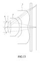
- FIG. 13 is a schematic view of a fourth embodiment of the imaging lens assembly according to the disclosure.
- FIG. 14 shows simulation results of spherical aberration, astigmatism, and distortional aberration of the fourth embodiment
- FIG. 15 shows a table of optical parameters for optical lens elements and a filter of the fourth embodiment
- FIG. 16 shows a table of parameters for aspheric surfaces of the fourth embodiment
- FIG. 17 is a schematic view of a fifth embodiment of the imaging lens assembly according to the disclosure.
- FIG. 18 shows simulation results of spherical aberration, astigmatism, and distortional aberration of the fifth embodiment
- FIG. 19 shows a table of optical parameters for optical lens elements and a filter of the fifth embodiment
- FIG. 20 shows a table of parameters for aspheric surfaces of the fifth embodiment.
- FIG. 21 shows a table of optical parameters for the first, second, third, fourth and fifth embodiments of the optical lens assembly according to the disclosure.
- an imaging lens assembly of the disclosure includes an optical lens set and a fixed aperture stop 4 .
- the optical lens set includes first, second and third optical lens elements 1 , 2 , 3 that are arranged sequentially from an object side to an image side along an optical axis of the imaging lens assembly.
- the first optical lens element 1 has a positive refractive power near the optical axis, a convex object-side surface that faces the object side, and a concave image-side surface that faces the image side.
- the second optical lens element 2 has a negative refractive power near the optical axis, and a convex image-side surface that faces the image side.
- At least one of an object-side surface and the image-side surface of the second optical lens element 2 is aspheric, and at least one of the object-side surface and the image-side surface of the second optical lens element 2 has an inflection point.
- the third optical lens element 3 has a positive refractive power near the optical axis, a convex object-side surface that faces the object side, and a concave image-side surface that faces the image side. At least one of the object-side surface and the image-side surface of the third optical lens element 3 has an inflection point.
- the fixed aperture stop 4 is disposed between the object side and the first optical lens element 1 .
- the imaging lens assembly of the disclosure satisfies the following optical conditions: 2.0 ⁇ OL/EPD ⁇ 2.5 (eq1); Vd 2 ⁇ Vd 3>20 (eq2); 0.25 ⁇ EPD/SD 32 ⁇ 0.35 (eq3); 0.28 ⁇ YC 32/ TL ⁇ 0.31 (eq4); 0 ⁇
- 0.262 mm,
- the object-side and image-side surfaces of the first, second and third optical lens elements 1 , 2 , 3 are all aspheric surfaces.
- An aspheric surface of the present disclosure satisfies the following equation:
- z is the z-component of the displacement of the aspheric surface from the vertex of the aspheric surface along the optical axis, at a distance h from the optical axis;
- k is a conic constant;
- c is the reciprocal of a radius of curvature; and
- A, B, C, E, F, G, H and J, etc. are aspheric coefficients.
- the aspheric surface may correct aberrations and decrease tolerance sensitivity, and may also contribute to the wider viewing angle of the imaging lens assembly.
- Equations 1 to 14 Equations 1 to 14 (eq1 to eq14).
- OL 2.396 mm
- EPD 1.075 mm
- f3 9.587 mm
- Vd3 30
- SD32 3.566 mm
- R1 1.184 mm
- R2 3.545 mm
- R3 ⁇ 6.111 mm
- R4 ⁇ 8.889 mm
- R5 1.075 mm
- ⁇ CT 1.779 mm
- f 2.408 mm
- f1 3.290 mm
- D12 0.419 mm
- D23 0.198 mm
- TL 3.353
- YC32 0.997 mm
- FOV 84.0,
- 0.337 mm,
- 0.341 mm
- CT3 0.733 mm.
- Equations 1 to 14 Equations 1 to 14 (eq1 to eq14).
- 0.385 mm,
- Equations 1 to 14 Equations 1 to 14 (eq1 to eq14).
- OL 2.457 mm
- EPD 1.097 mm
- f3 13.518 mm
- SD32 3.582 mm
- R1 1.062 mm
- R2 3.208 mm
- R3 ⁇ 5.012 mm
- R4 ⁇ 6.105 mm
- R5 1.105 mm
- ⁇ CT 1.939 mm
- f 2.227 mm
- f1 2.917 mm
- D12 0.317 mm
- D23 0.201 mm
- TL 3.350 mm
- YC32 0.976 mm
- FOV 87.0
- 0.385 mm
- 0.420 mm
- CT3 0.709 mm.
- Equations 1 to 14 Equations 1 to 14 (eq1 to eq14).
- 0.293 mm,
- Equations 1 to 14 Equations 1 to 14 (eq1 to eq14).
- the imaging lens assembly of the disclosure satisfies Equations 1 to 14, thereby increasing a resolving power thereof, enlarging a maximum viewing angle thereof, and decreasing the overall thickness thereof.
Landscapes
- Physics & Mathematics (AREA)
- General Physics & Mathematics (AREA)
- Optics & Photonics (AREA)
- Lenses (AREA)
Abstract
Description
2.0<OL/EPD<2.5,
Vd2−Vd3>20,
0.25<EPD/SD32<0.35,
in which, OL represents a distance between the object-side surface of the first optical lens and the image-side surface of the third optical lens element along the optical axis, EPD represents an entrance pupil diameter of the imaging lens assembly, Vd2 represents the Abbe number of the second optical lens element, Vd3 represents the Abbe number of the third optical lens element, and SD32 represents a maximum clear aperture of the image-side surface of the third optical lens element.
2.0<OL/EPD<2.5,
0<f3/Vd3>1.5,
0.3<|SAG31|/CT3<0.6,
in which, OL represents a distance between the object-side surface of the first optical lens and the image-side surface of the third optical lens along the optical axis, EPD represents an entrance pupil diameter of said imaging lens assembly, f3 represents a focal length of said third optical lens element, Vd3 represents the Abbe number of said third optical lens element, |SAG31| represents a distance along the optical axis between a center of the object-side surface of said third optical lens element and a projection on the optical axis of a point of maximum clear aperture of said object-side surface of said third optical lens element, and CT3 represents a thickness of said third optical lens element along the optical axis.
2.0<OL/EPD<2.5 (eq1);
Vd2−Vd3>20 (eq2);
0.25<EPD/SD32<0.35 (eq3);
0.28<YC32/TL<0.31 (eq4);
0<|Vd1−Vd2|<5 (eq5);
1.4<D12/D23<2.4 (eq6);
2.2<TL/R1<3.5 (eq7);
0.1<D12/f1<0.2 (eq8);
0.5<ΣCT/f<1 (eq9);
−3.0<(R2−R3)/(R4+R5)<−1.0 (eq10);
76<FOV<88 (eq11);
0<f3/Vd3<1.5 (eq12);
0.3<|SAG31|/CT3<0.6 (eq13);
and
0.50<|SAG22|+|SAG31|<0.65 (eq14),
in which, OL represents a distance between the object-side surface of the first optical lens and the image-side surface of the third optical lens element along the optical axis, EPD represents an entrance pupil diameter of the imaging lens assembly, Vd2 represents the Abbe number of the second optical lens element 2, Vd3 represents the Abbe number of the third optical lens element 3, SD32 represents a maximum clear aperture of the image-side surface of the third optical lens element 3, YC32 represents a distance along a plane perpendicular to the optical axis between the optical axis and a point C on the image-side surface of the third optical lens element 3 to which the plane is tangential, where there is at least the point C on the image-side surface of the third optical lens element 3 to which the plane is tangential, TL represents a distance from an imaging plane to the object-side surface of the first optical lens element 1 along the optical axis, Vd1 represents the Abbe number of the first optical lens element 1, Vd2 represents the Abbe number of the second optical lens element 2, D12 represents a distance between the first and second optical lens elements 1,2 along the optical axis, D23 represents a distance between the second and third optical lens elements 2, 3 along the optical axis, R1 represents a radius of curvature of the object-side surface of the first optical lens element 1, f1 represents a focal length of the first optical lens element 1, ΣCT represents a sum of thicknesses of the first, second and third optical lens elements 1, 2, 3 along the optical axis, f represents a focal length of the imaging lens assembly, R2 represents a radius of curvature of the image-side surface of the first optical lens element 1, R3 represents a radius of curvature of the object-side surface of the second optical lens element 2, R4 represents a radius of curvature of the image-side surface of the second optical lens element 2, R5 represents a radius of curvature of the object-side surface of the third optical lens element 3, FOV represents a maximum field-of-view of the imaging lens assembly, f3 represents a focal length of the third optical lens element 3, |SAG31| represents a distance along the optical axis between a center of the object-side surface of the third optical lens element 3 and a projection on the optical axis of a point of maximum clear aperture of the object-side surface of the third optical lens element 3, CT3 represents a thickness of the third optical lens element 3 along the optical axis, and |SAG22| represents a distance along the optical axis between a center of the image-side surface of the second optical lens element 2 and a projection on the optical axis of a point of maximum clear aperture of the image-side surface of the second optical lens element 2. The first, second and third
Claims (11)
2.0<OL/EPD<2.5,
Vd2−Vd3>20,
0.25<EPD/SD32<0.35,
0.28<YC32/TL<0.31,
0<|Vd1−Vd21<5,
1.4<D12/D23<2.4,
2.2<TL/R1<3.5,
0.1<D12/f1<0.2,
0.5<ΣCT/f<1,
−3.0<(R2−R3)/(R4+R5)<−1.0,
76<FOV<88,
Applications Claiming Priority (3)
| Application Number | Priority Date | Filing Date | Title |
|---|---|---|---|
| TW103133037 | 2014-09-24 | ||
| TW103133037A | 2014-09-24 | ||
| TW103133037A TWI524090B (en) | 2014-09-24 | 2014-09-24 | Wide angle imaging lens group |
Publications (2)
| Publication Number | Publication Date |
|---|---|
| US20160085051A1 US20160085051A1 (en) | 2016-03-24 |
| US9541733B2 true US9541733B2 (en) | 2017-01-10 |
Family
ID=55525612
Family Applications (1)
| Application Number | Title | Priority Date | Filing Date |
|---|---|---|---|
| US14/858,521 Active US9541733B2 (en) | 2014-09-24 | 2015-09-18 | Imaging lens assembly |
Country Status (2)
| Country | Link |
|---|---|
| US (1) | US9541733B2 (en) |
| TW (1) | TWI524090B (en) |
Families Citing this family (2)
| Publication number | Priority date | Publication date | Assignee | Title |
|---|---|---|---|---|
| KR101780432B1 (en) * | 2015-12-18 | 2017-09-21 | 주식회사 코렌 | Photographic lens optical system |
| TWI827857B (en) * | 2020-07-03 | 2024-01-01 | 先進光電科技股份有限公司 | Optical image capturing system |
Citations (1)
| Publication number | Priority date | Publication date | Assignee | Title |
|---|---|---|---|---|
| US20070229987A1 (en) * | 2006-03-28 | 2007-10-04 | Fujinon Corporation | Imaging Lens |
-
2014
- 2014-09-24 TW TW103133037A patent/TWI524090B/en active
-
2015
- 2015-09-18 US US14/858,521 patent/US9541733B2/en active Active
Patent Citations (1)
| Publication number | Priority date | Publication date | Assignee | Title |
|---|---|---|---|---|
| US20070229987A1 (en) * | 2006-03-28 | 2007-10-04 | Fujinon Corporation | Imaging Lens |
Also Published As
| Publication number | Publication date |
|---|---|
| US20160085051A1 (en) | 2016-03-24 |
| TW201612580A (en) | 2016-04-01 |
| TWI524090B (en) | 2016-03-01 |
Similar Documents
| Publication | Publication Date | Title |
|---|---|---|
| TWI589948B (en) | Imaging lens assembly, image capturing unit and electronic device | |
| CN104169773B (en) | Imaging lens and imaging device | |
| US9158094B1 (en) | Imaging lens, and electronic apparatus including the same | |
| US9103962B2 (en) | Wide-angle optical lens assembly | |
| US9036274B2 (en) | Image capturing optical lens system | |
| US9557531B2 (en) | Imaging lens and imaging apparatus equipped with the imaging lens | |
| US9274312B2 (en) | Imaging lens assembly | |
| US8760775B2 (en) | Imaging lens and imaging apparatus including the imaging lens | |
| US9335515B2 (en) | Imaging lens and imaging device provided with the same | |
| US20130070346A1 (en) | Optical image capturing lens assembly | |
| US20130279021A1 (en) | Optical image lens system | |
| US20130033764A1 (en) | Image capturing optical lens assembly | |
| US20130235473A1 (en) | Optical image system | |
| US9488799B2 (en) | Imaging lens and imaging device provided with the same | |
| US20130201568A1 (en) | Image capturing optical lens system | |
| US20130321932A1 (en) | Image capturing optical lens assembly | |
| US20120314301A1 (en) | Optical image capturing lens assembly | |
| US20130050847A1 (en) | Image lens assembly | |
| US20190049698A1 (en) | Optical lens | |
| US9335516B2 (en) | Imaging lens and imaging device provided with the same | |
| JP2016114633A (en) | Image capturing lens and image capturing device | |
| TW201807451A (en) | Imaging lens system, image capturing unit and electronic device | |
| US9360657B2 (en) | Imaging lens module | |
| TWM500897U (en) | Imaging lens and imaging apparatus equipped with the imaging lens | |
| US9207432B2 (en) | Imaging lens and imaging device provided with the same |
Legal Events
| Date | Code | Title | Description |
|---|---|---|---|
| AS | Assignment |
Owner name: ABILITY OPTO-ELECTRONICS TECHNOLOGY CO., LTD., TAI Free format text: ASSIGNMENT OF ASSIGNORS INTEREST;ASSIGNOR:LEE, HUNG-WEN;REEL/FRAME:036602/0073 Effective date: 20150911 |
|
| STCF | Information on status: patent grant |
Free format text: PATENTED CASE |
|
| MAFP | Maintenance fee payment |
Free format text: PAYMENT OF MAINTENANCE FEE, 4TH YEAR, LARGE ENTITY (ORIGINAL EVENT CODE: M1551); ENTITY STATUS OF PATENT OWNER: LARGE ENTITY Year of fee payment: 4 |
|
| MAFP | Maintenance fee payment |
Free format text: PAYMENT OF MAINTENANCE FEE, 8TH YEAR, LARGE ENTITY (ORIGINAL EVENT CODE: M1552); ENTITY STATUS OF PATENT OWNER: LARGE ENTITY Year of fee payment: 8 |