US9536697B2 - System and method for calibrating charge-regulating module - Google Patents
System and method for calibrating charge-regulating module Download PDFInfo
- Publication number
- US9536697B2 US9536697B2 US14/716,385 US201514716385A US9536697B2 US 9536697 B2 US9536697 B2 US 9536697B2 US 201514716385 A US201514716385 A US 201514716385A US 9536697 B2 US9536697 B2 US 9536697B2
- Authority
- US
- United States
- Prior art keywords
- charge
- regulation module
- beam spot
- sample
- laser
- Prior art date
- Legal status (The legal status is an assumption and is not a legal conclusion. Google has not performed a legal analysis and makes no representation as to the accuracy of the status listed.)
- Active
Links
Images


Classifications
-
- H—ELECTRICITY
- H01—ELECTRIC ELEMENTS
- H01J—ELECTRIC DISCHARGE TUBES OR DISCHARGE LAMPS
- H01J37/00—Discharge tubes with provision for introducing objects or material to be exposed to the discharge, e.g. for the purpose of examination or processing thereof
- H01J37/02—Details
- H01J37/026—Means for avoiding or neutralising unwanted electrical charges on tube components
-
- H—ELECTRICITY
- H01—ELECTRIC ELEMENTS
- H01J—ELECTRIC DISCHARGE TUBES OR DISCHARGE LAMPS
- H01J37/00—Discharge tubes with provision for introducing objects or material to be exposed to the discharge, e.g. for the purpose of examination or processing thereof
- H01J37/02—Details
- H01J37/244—Detectors; Associated components or circuits therefor
-
- H—ELECTRICITY
- H01—ELECTRIC ELEMENTS
- H01J—ELECTRIC DISCHARGE TUBES OR DISCHARGE LAMPS
- H01J37/00—Discharge tubes with provision for introducing objects or material to be exposed to the discharge, e.g. for the purpose of examination or processing thereof
- H01J37/26—Electron or ion microscopes; Electron or ion diffraction tubes
- H01J37/261—Details
- H01J37/265—Controlling the tube; circuit arrangements adapted to a particular application not otherwise provided, e.g. bright-field-dark-field illumination
-
- H—ELECTRICITY
- H01—ELECTRIC ELEMENTS
- H01J—ELECTRIC DISCHARGE TUBES OR DISCHARGE LAMPS
- H01J37/00—Discharge tubes with provision for introducing objects or material to be exposed to the discharge, e.g. for the purpose of examination or processing thereof
- H01J37/26—Electron or ion microscopes; Electron or ion diffraction tubes
- H01J37/28—Electron or ion microscopes; Electron or ion diffraction tubes with scanning beams
-
- H—ELECTRICITY
- H01—ELECTRIC ELEMENTS
- H01J—ELECTRIC DISCHARGE TUBES OR DISCHARGE LAMPS
- H01J2237/00—Discharge tubes exposing object to beam, e.g. for analysis treatment, etching, imaging
- H01J2237/004—Charge control of objects or beams
- H01J2237/0041—Neutralising arrangements
- H01J2237/0044—Neutralising arrangements of objects being observed or treated
- H01J2237/0047—Neutralising arrangements of objects being observed or treated using electromagnetic radiations, e.g. UV, X-rays, light
-
- H—ELECTRICITY
- H01—ELECTRIC ELEMENTS
- H01J—ELECTRIC DISCHARGE TUBES OR DISCHARGE LAMPS
- H01J2237/00—Discharge tubes exposing object to beam, e.g. for analysis treatment, etching, imaging
- H01J2237/02—Details
- H01J2237/024—Moving components not otherwise provided for
Definitions
- the present invention relates to a system and method for calibrating charge-regulating module, and more particularly to a charged particle beam system with a calibratable charge-regulating module.
- a process for manufacturing semiconductor devices comprises the operation of forming layers of a variety of materials on or in the substrate of each semiconductor device; photo-processing, masking and forming circuit patterns on the semiconductor device; and removing or etching portions of the layers to form the semiconductor device.
- Such semiconductor devices are manufactured by repeating these and other operations on each device of a semiconductor wafer. Better manufacturing techniques have allowed for micro fabrication, resulting in features that are much less visible by most observation tools. Inspections of the wafer are made to check for obtaining defect free devices. In view of this requirement, charged particle beam systems, e.g. scanning electron microscopes (SEMs), electron beam probers and focused ion beam (FIB) systems, are used in such purpose.
- SEMs scanning electron microscopes
- FIB focused ion beam
- Charges on a wafer sample may be accumulated when scanned by the current charged particle beam tools, particularly for the ebeam inspection tool due to larger beam current requirement, and quality of the acquired image will thus be deteriorated due to the accumulated charges on the surface of the wafer sample. Critical defects then can be hardly identified.
- a charge regulation method is provided to regulate or control charge conditions wafer surface.
- One charge regulation module is to use Laser illuminating onto the wafer surface, and charged can be regulated due to photoconductivity and/or photoelectric effect.
- the illuminated area by Laser may be deviated from the point irradiated by the charged particle beam on the wafer surface due to installation or operation of the charged particle tool, and charge conditions thereon may be again deteriorated little by little.
- a calibration is thus necessary.
- the charged particle tool is built within a vacuum chamber, and the calibration procedure of charge-regulation module means to breakdown the vacuum environment to atmosphere in the chamber. After the charge-regulation module is calibrated, the chamber has to be processed to vacuum environment. Such a calibration procedure is a time-consuming schedule, about 2-days or longer.
- the present invention provides a system and a method for calibrating charge-regulation module in vacuum environment.
- the charge-regulation module provides a beam on a sample surface and charges on the sample surface can be regulated. A beam spot is thus formed on the sample surface.
- Means for mounting charge-regulation module can provide motions to the charge-regulation module such that the beam spot on the sample surface can be moved to a pre-determined position which is irradiated by a charged particle beam.
- charge environment of a sample wafer or mask a primary electron beam irradiates the pre-determined position, and charges of the pre-determined position can be regulated.
- One embodiment of the present invention provides a system for calibrating a charge-regulating module, which comprises means for mounting a Laser and providing motions to move the Laser, a detector, a controller coupled to the detector, and a transmission coupled to the controller.
- the Laser illuminates a beam on a surface of a sample with a beam spot thereon, and regulates charges on the sample surface.
- the detector receives a reflected beam from the beam spot on the sample surface.
- the controller receives signals from the detector, calculates a position of the beam spot, and controls the beam spot to a pre-determined location.
- the transmission drives the mounting means such that the beam spot can be moved to the pre-determined position.
- the mounting means is fastened to an objective lens of a charged particle beam tool, and the pre-determined location is irradiated by a charged particle beam of the charged particle beam tool.
- the charged particle beam tool could be an ebeam inspection tool and the sample could be a wafer or a mask.
- the mounting means may include a first motor for driving the Laser with a rotational motion, and a second motor for driving the Laser with a vertical motion.
- the transmission is a hollow rod within wires for providing powers and instructions to the first and second motors.
- the mounting means in another embodiment, may be a C-shape mount and the Laser is fastened thereto.
- the transmission includes a rotation-to-translation means and a carved body not only fastened to the rotation-to-translation means but also engaged to the C-shape mount. A portion of the C-shape mount, engaged with the carved body, is forced to distort in vertical motion and to expand with horizontal motion.
- an ebeam inspection tool which comprises an electron tip for providing an electron source, an anode for extracting the electron source as a primary electron beam, a condenser lens for condensing the primary electron beam, a magnetic objective lens for focusing the primary electron beam on a surface of a sample, a charge-regulation module for regulating charges in the sample surface, and a system for calibrating the charge-regulation module.
- the charge-regulation module is fastened to the magnetic objective lens.
- the system for calibrating the charge-regulation module includes means for mounting the charge-regulation module and providing motions to move the charge-regulation module, a detector, a controller coupled to the detector, and a transmission coupled to the controller.
- the charge-regulation module illuminates a beam on a surface of a sample with a beam spot thereon.
- the detector receives a reflected beam from the beam spot on the sample surface.
- the controller receives signals from the detector, calculates a position of the beam spot, and controls the beam spot to a pre-determined location.
- the transmission drives the mounting means such that the beam spot is moved to the pre-determined location.
- the sample in the embodiment, is a wafer or a mask.
- the mounting means may include a first motor for driving the charge-regulation module with a rotational motion, and a second motor for driving the charge-regulation module with a vertical motion.
- the transmission is a hollow rod within wires for providing powers and instructions to the first and second motors.
- the mounting means in another embodiment, may be a C-shape mount and the charge-regulation module is fastened thereto.
- the transmission includes a rotation-to-translation means, and a carved body not only fastened to the rotation-to-translation means but also engaged to the C-shape mount. A portion of the C-shape mount, engaged with the carved body, is forced to distort in vertical motion and the portion of the C-shape mount is forced to expand with horizontal motion.
- the present invention also provides a method for calibrating a charge-regulation module under vacuum environment, which comprises steps of providing a beam on a surface of a sample by the charge-regulation module to form a beam spot on the surface, detecting a location of the beam spot, calculating a pre-determined position of a charged particle beam on the surface, and driving the charge-regulation module such that the beam spot moves to the pre-determined position.
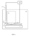
- FIG. 1 is a schematic diagram of a charged particle beam system according to one embodiment of the invention.
- FIG. 2 illustrates an embodiment of a calibratable charge regulation module according to the present invention.
- FIG. 3A is a top view for illustrating an operation for calibrating the charge regulation module according to one embodiment of the invention.
- FIG. 3B is a side view for illustrating an operation for calibrating the charge regulation module according to one embodiment of the invention.
- FIG. 3C is schematic diagram of an operation for calibrating the charge regulation module according to one embodiment of the invention.
- FIG. 4A is a top view for illustrating an operation for calibrating the charge regulation module according to another embodiment of the invention.
- FIG. 4B is a side view for illustrating an operation for calibrating the charge regulation module according to another embodiment of the invention.
- FIG. 5 is a schematic diagram of Laser beam spot on surface of wafer sample in an embodiment of the present invention.
- FIGS. 6A and 6B illustrate a rotation-to-translation means in an embodiment of the present invention.
- FIG. 7 illustrates several paths of Laser beam spot on the surface of the wafer sample when the charge regulation module is calibrated in one embodiment of the present invention.
- FIG. 8 illustrates a cross-sectional, side view of the charge regulation module mounted to the yoke and operated to the wafer sample.
- FIG. 9 illustrates details of the transmission through a wall of the vacuum chamber in one embodiment of the present invention.
- calibtrable in the present invention means the charge regulation module is capable of being calibrated.
- beam in the present invention means electron beam.
- charged particle beam tools may be SEM (Scanning Electron Microscope), TEM (Tunneling Electron Microscope), STEM (Scanning Tunneling Electron Microscope), AFM (Atomic force Microscope), or FIB (Focused Ion Beam).
- SEM Sccanning Electron Microscope
- TEM Transmission Electron Microscope
- STEM Scanning Tunneling Electron Microscope
- AFM Atomic force Microscope
- FIB Fluorused Ion Beam
- a SEM-based ebeam inspection tool can be referred to FIG. 1 .
- the SEM 100 includes an electron gun and a column, wherein the electron gun includes a tip 101 , a Schottky suppressor electrode 102 , an anode 103 , a selectable Coulomb aperture plate 104 , and a condenser lens 110 .
- the tip 101 emitting a primary electron beam 190 , can be a high temperature Schottky point cathode which is ZrO/W Schottky electrode.
- the Schottky suppressor electrode 102 provides a virtual source of the primary electron beam 190 .
- the anode electrode 103 provides an electric field to extract electrons from the tip 101 .
- the condenser lens 110 in the FIG. 1 , is an electrostatic lens, but, for any person skilled in the art, one or more than one magnetic lens can also be applied to the SEM 100 .
- the column in the SEM 100 includes a beam current plate 120 , a detector 170 , two deflectors 141 and 142 , and an objective lens 130 .
- the beam current plate 120 includes a plurality of apertures, is for users to select suitable beam current of the primary electron beam.
- the primary electron beam is then focused by the objective lens 130 on the wafer sample 1 supported by a stage 10 .
- the sample 1 in the present invention can be a mask for lithographic process, a silicon wafer, a GaAs wafer, a SiC wafer, or any other substrate for semiconductor process.
- the objective lens 130 in FIG. 1 , is a magnetic lens which includes a coil 132 encompassed by a yoke 131 .
- Two deflectors 141 and 142 deflect to scan the primary electron beam 190 on the wafer sample 1 .
- An electrode 150 below the objective lens 130 can provide a retarding or immersion electric field for the primary electron beam 190 .
- a potential can be applied to the stage 10 such that landing energy of the primary electron beam 190 can be adjusted or controlled.
- the objective lens 130 illustrated in FIG. 1 is a basic, common one in commercial SEM, but variant designs and structures for specific purposes can be also applied to the present invention, such as SORIL lens, for large FOV (Field Of View) inspection, provided by Chen et al in the U.S. Pat. No. 6,392,231.
- the charge regulation module in the present invention can be referred to FIG. 2 , wherein a Laser 320 illuminates a specific electromagnetic wave on a surface of the wafer sample 1 and a beam spot is formed on a surface of the sample 1 .
- the electromagnetic wave is then reflected to a detector 325 which may be CCD (Charge-Coupled Device) or CMOS(Complementary Metal-Oxide-Semiconductor) sensor.
- CCD Charge-Coupled Device
- CMOS Complementary Metal-Oxide-Semiconductor
- a controller 300 After the detector 325 receiving signals from the Laser 320 , a controller 300 detects a location of the beam spot on the surface of the sample 1 , calculates a pre-determined position which is irradiated by the primary electron beam 190 , and drives the Laser 320 to illuminate the beam spot to the pre-determined position via the transmission 310 .
- the SEM 100 , the Laser 210 , the detector 325 , the wafer sample 1 , and the stage 10 are all inside the vacuum chamber 200 .
- the controller 300 may be a computer or ASIC (Application Specific Integrated Circuit), is always outside the vacuum chamber 200 .
- the transmission 310 is the only one through the vacuum chamber 200 .
- a first embodiment of the present invention can be referred to FIG. 3A , FIG. 3B , and FIG. 3C .
- a mount 330 fastened to the yoke 131 , is for holding the Laser 320 , and the transmission 310 can directly control the Laser 320 in a rotational motion 400 by a motor 331 .
- the mount 330 can be driven by another motor 332 with a vertical motion 402 . Therefore, the Laser 320 can be adjusted by using the two motions 400 and 402 such that spot of the Laser 320 on wafer sample can be controlled at desired locations.
- the transmission 310 in this embodiment may be designed as a hollow rod within electric wires inside to provide instructions and powers to the both motors.
- FIG. 4A and FIG. 4B Another embodiment of the present invention, which can be referred to FIG. 4A and FIG. 4B , that one motion transmission could provide the charge regulation module calibrated in desired locations on the wafer sample.
- a C-shape mount 340 fastened to the yoke 131 , with a clamp 342 such that the mount 340 could have a little flexibility, which could be expanded or suppressed at the open ends.
- Laser 320 is mounted to the C-shape mount 340 without any degree of freedom to move.
- the transmission 310 which is a solid rod in this embodiment, can provide a rotation motion 400 and fastened with a rotation-to-translation means 312 .
- the rotation-to-translation means 312 is attached with a carved body 318 such that the carved body 318 has a vertical motion 402 .
- the carved body 318 has a declined surface which is engaged with the C-shape mount 340 .
- the C-shape mount 340 is forced to distort in two directions. The first is that the contact surface of the mount 340 with the carved body 318 will be forced in vertical motion 402 , and the second is that the contact portion between the mount 340 and the carved body 318 will be forced in horizontal motion 404 .
- the C-shape mount 340 has a clamp 342 , the open ends of the mount 340 will be enlarged a little.
- spot illuminated by the Laser 320 on surface of the wafer sample 1 is illustrated. Due to there are two motions applied to the Laser 320 simultaneously, the spot will move in two directions on the surface of the wafer sample 1 .
- FIG. 6A and FIG. 6B One detail embodiment of the rotation-to-translation means 312 can be referred to FIG. 6A and FIG. 6B , wherein one end of the transmission 310 is a screw body 313 and engaged with gears 314 .
- the transmission 310 rotates 400
- the carved body 318 will moved vertically 402 due to operations of the gears 314 and screw 313 .
- Any means, combined by screws/gears or other parts, for transferring the rotation to translation motions could be applied to this invention.
- Detail path 500 of the spot on the surface can be referred to FIG. 7 , where three paths are illustrated for example with one spot 510 illuminated by the Laser 320 .
- the spot on surface of the wafer sample will also move along a curve line. It is because the two motions combined together and ratio between expansion of C-shape mount due to horizontal motion 404 and downward of C-shape mount 340 due to vertical motion 402 is not linear. However, when the transmission 310 is rotated back, the beam spot won't trace back. It is because that when external forces applied to the mount 340 is released, the two directions of distorted mount 340 won't be returned back to the original shape simultaneously.
- the beam spot 510 in FIG. 7 when the transmission 310 is rotated back, the beam spot 510 will move back along a new path to the original and a closed loop is formed. There are three paths in FIG. 7 to illustrate the beam spot will overlap along a curve when it moved from the original location, and the beam spot will divert to three different paths when different rotation back point of the transmission 310 is triggered. Therefore, in the present invention, all possible paths should be recorded for user to adjust the Laser 320 .
- FIG. 8 a side, sectional view is illustrated, wherein the Laser 320 is fastened to the mount 330 / 340 and illuminates a beam spot on the wafer sample 1 .
- the working distance between yoke 131 and wafer sample 1 is always short compared to the scale of the yoke 131 . Therefore, the angle between beam and the wafer sample 1 is very close to about 1-10 degree. Due to the ebeam spot size is much smaller than the Laser beam spot, locations of the Laser beam spot to be calibrated is limited to a small range.
- the transmission 310 will couple to the controller 300 and directly drive to the mount 330 / 340 , it will exist in atmosphere and vacuum environments.
- the transmission 310 should be through wall 202 of the vacuum chamber 200 .
- a seal 210 encompasses the transmission 310 and an O-ring 212 is used inside the seal 210 to further seal the vacuum.
- Top surface 311 of the transmission 310 may have a structure 311 for rotation motion 400 .
- a method for calibrating a charge-regulation module under vacuum environment comprises steps of providing a beam on a surface of a sample by the charge-regulation module to form a beam spot on the surface, detecting a location of the beam spot, calculating a pre-determined position of a charged particle beam on the surface, and driving the charge-regulation module such that the beam spot moves to the pre-determined position.
- a method for calibrating the charge-regulation module in vacuum environment comprises steps of registering a location of the charge particle beam irradiated to the sample surface, receiving a reflected optical beam from the sample surface and illuminated by a Laser, calculating a position of the optical beam, and adjusting the Laser to illuminate the optical beam to the location of the charged particle beam on the sample surface.
- the procedures could be finished within several minutes in a vacuum environment, without days of the processing vacuum chamber.
Landscapes
- Chemical & Material Sciences (AREA)
- Analytical Chemistry (AREA)
- Analysing Materials By The Use Of Radiation (AREA)
- Testing Or Measuring Of Semiconductors Or The Like (AREA)
Abstract
Description
Claims (21)
Priority Applications (2)
| Application Number | Priority Date | Filing Date | Title |
|---|---|---|---|
| US14/716,385 US9536697B2 (en) | 2015-05-19 | 2015-05-19 | System and method for calibrating charge-regulating module |
| TW104118435A TWI585805B (en) | 2015-05-19 | 2015-06-05 | System and method for calibrating charge-regulating module and ebeam inspection tool |
Applications Claiming Priority (1)
| Application Number | Priority Date | Filing Date | Title |
|---|---|---|---|
| US14/716,385 US9536697B2 (en) | 2015-05-19 | 2015-05-19 | System and method for calibrating charge-regulating module |
Publications (2)
| Publication Number | Publication Date |
|---|---|
| US20160343534A1 US20160343534A1 (en) | 2016-11-24 |
| US9536697B2 true US9536697B2 (en) | 2017-01-03 |
Family
ID=57325598
Family Applications (1)
| Application Number | Title | Priority Date | Filing Date |
|---|---|---|---|
| US14/716,385 Active US9536697B2 (en) | 2015-05-19 | 2015-05-19 | System and method for calibrating charge-regulating module |
Country Status (2)
| Country | Link |
|---|---|
| US (1) | US9536697B2 (en) |
| TW (1) | TWI585805B (en) |
Cited By (3)
| Publication number | Priority date | Publication date | Assignee | Title |
|---|---|---|---|---|
| US11002687B2 (en) * | 2016-03-16 | 2021-05-11 | Hitachi High-Tech Corporation | Defect inspection method and defect inspection device |
| US11728131B2 (en) | 2020-12-16 | 2023-08-15 | Asml Netherlands B.V. | Thermal-aided inspection by advanced charge controller module in a charged particle system |
| US12105036B2 (en) | 2018-09-13 | 2024-10-01 | Asml Netherlands B.V. | Method and apparatus for monitoring beam profile and power |
Families Citing this family (7)
| Publication number | Priority date | Publication date | Assignee | Title |
|---|---|---|---|---|
| US9673023B2 (en) | 2015-05-12 | 2017-06-06 | Applied Materials Israel Ltd. | System for discharging an area that is scanned by an electron beam |
| US10168614B1 (en) | 2017-06-14 | 2019-01-01 | Applied Materials Israel Ltd. | On-axis illumination and alignment for charge control during charged particle beam inspection |
| CN108646167B (en) * | 2018-04-27 | 2020-12-04 | 中科晶源微电子技术(北京)有限公司 | Laser-assisted electron beam inspection apparatus and method for semiconductor devices |
| US20220375715A1 (en) * | 2019-10-24 | 2022-11-24 | Asml Netherlands B.V. | Charged particle inspection system and method using multi-wavelength charge controllers |
| EP4084039A1 (en) * | 2021-04-29 | 2022-11-02 | ASML Netherlands B.V. | Charged particle assessment system and method |
| WO2023160959A1 (en) * | 2022-02-23 | 2023-08-31 | Asml Netherlands B.V. | Beam manipulation using charge regulator in a charged particle system |
| US20240420917A1 (en) * | 2023-06-15 | 2024-12-19 | Applied Materials Israel Ltd. | Discharging a region of a sample |
Citations (7)
| Publication number | Priority date | Publication date | Assignee | Title |
|---|---|---|---|---|
| US6392231B1 (en) | 2000-02-25 | 2002-05-21 | Hermes-Microvision, Inc. | Swinging objective retarding immersion lens electron optics focusing, deflection and signal collection system and method |
| US6465781B1 (en) * | 1999-06-11 | 2002-10-15 | Hitachi, Ltd. | Method and apparatus for inspecting or measuring a sample based on charged-particle beam imaging, and a charged-particle beam apparatus |
| US20030213893A1 (en) * | 2002-05-16 | 2003-11-20 | Ebara Corporation | Electron beam apparatus and device manufacturing method using same |
| US20050051722A1 (en) * | 2003-09-10 | 2005-03-10 | Hiroshi Makino | Inspection system, inspection method, and process management method |
| US7211796B2 (en) * | 2003-05-27 | 2007-05-01 | Kabushiki Kaisha Toshiba | Substrate inspection apparatus, substrate inspection method and method of manufacturing semiconductor device |
| US7863565B2 (en) * | 2007-06-19 | 2011-01-04 | Hitachi, Ltd. | Electron beam inspection method and electron beam inspection apparatus |
| US20140070113A1 (en) * | 2012-09-07 | 2014-03-13 | Fei Company | Automated Method for Coincident Alignment of a Laser Beam and a Charged Particle Beam |
Family Cites Families (3)
| Publication number | Priority date | Publication date | Assignee | Title |
|---|---|---|---|---|
| CN1244133C (en) * | 2000-05-25 | 2006-03-01 | 瓦里安半导体设备联合公司 | Method and apparatus for particle detection |
| WO2007067296A2 (en) * | 2005-12-02 | 2007-06-14 | Alis Corporation | Ion sources, systems and methods |
| JP2009200105A (en) * | 2008-02-19 | 2009-09-03 | Canon Inc | Exposure device |
-
2015
- 2015-05-19 US US14/716,385 patent/US9536697B2/en active Active
- 2015-06-05 TW TW104118435A patent/TWI585805B/en active
Patent Citations (7)
| Publication number | Priority date | Publication date | Assignee | Title |
|---|---|---|---|---|
| US6465781B1 (en) * | 1999-06-11 | 2002-10-15 | Hitachi, Ltd. | Method and apparatus for inspecting or measuring a sample based on charged-particle beam imaging, and a charged-particle beam apparatus |
| US6392231B1 (en) | 2000-02-25 | 2002-05-21 | Hermes-Microvision, Inc. | Swinging objective retarding immersion lens electron optics focusing, deflection and signal collection system and method |
| US20030213893A1 (en) * | 2002-05-16 | 2003-11-20 | Ebara Corporation | Electron beam apparatus and device manufacturing method using same |
| US7211796B2 (en) * | 2003-05-27 | 2007-05-01 | Kabushiki Kaisha Toshiba | Substrate inspection apparatus, substrate inspection method and method of manufacturing semiconductor device |
| US20050051722A1 (en) * | 2003-09-10 | 2005-03-10 | Hiroshi Makino | Inspection system, inspection method, and process management method |
| US7863565B2 (en) * | 2007-06-19 | 2011-01-04 | Hitachi, Ltd. | Electron beam inspection method and electron beam inspection apparatus |
| US20140070113A1 (en) * | 2012-09-07 | 2014-03-13 | Fei Company | Automated Method for Coincident Alignment of a Laser Beam and a Charged Particle Beam |
Cited By (4)
| Publication number | Priority date | Publication date | Assignee | Title |
|---|---|---|---|---|
| US11002687B2 (en) * | 2016-03-16 | 2021-05-11 | Hitachi High-Tech Corporation | Defect inspection method and defect inspection device |
| US12105036B2 (en) | 2018-09-13 | 2024-10-01 | Asml Netherlands B.V. | Method and apparatus for monitoring beam profile and power |
| US11728131B2 (en) | 2020-12-16 | 2023-08-15 | Asml Netherlands B.V. | Thermal-aided inspection by advanced charge controller module in a charged particle system |
| US12125669B2 (en) | 2020-12-16 | 2024-10-22 | Asml Netherlands B.V. | Thermal-aided inspection by advanced charge controller module in a charged particle system |
Also Published As
| Publication number | Publication date |
|---|---|
| TW201642301A (en) | 2016-12-01 |
| TWI585805B (en) | 2017-06-01 |
| US20160343534A1 (en) | 2016-11-24 |
Similar Documents
| Publication | Publication Date | Title |
|---|---|---|
| US9536697B2 (en) | System and method for calibrating charge-regulating module | |
| CN101630623B (en) | Inspection apparatus by charged particle beam and method for manufacturing device using inspection apparatus | |
| US6509750B1 (en) | Apparatus for detecting defects in patterned substrates | |
| US9728374B2 (en) | Inspection apparatus | |
| TWI491873B (en) | Inspection method, inspection device and electronic wire device | |
| US20080035860A1 (en) | Dual beam system | |
| JP2005249745A (en) | Sample surface inspecting method and inspecting apparatus | |
| CN113646865B (en) | Multi-beam inspection equipment with single-beam mode | |
| US7560691B1 (en) | High-resolution auger electron spectrometer | |
| US12278081B2 (en) | System and method for alignment of secondary beams in multi-beam inspection apparatus | |
| US11621142B2 (en) | Substrate positioning device and electron beam inspection tool | |
| KR20180133835A (en) | Method for imaging wafer with focused charged particle beam in semiconductor fabrication | |
| JP4642362B2 (en) | Substrate alignment method, substrate surface inspection method, substrate positioning method, semiconductor device manufacturing method, substrate alignment apparatus, and substrate surface inspection apparatus | |
| WO2018154705A1 (en) | Charged particle beam device | |
| JP5302934B2 (en) | Sample surface inspection method and inspection apparatus | |
| TWI834093B (en) | Dual focus solution for sem metrology tools | |
| EP3599632A1 (en) | Substrate positioning device with remote temperature sensor | |
| US20240021404A1 (en) | Charged-particle beam apparatus with beam-tilt and methods thereof | |
| JP4387262B2 (en) | Charged particle beam apparatus and microdevice manufacturing method | |
| WO2023094098A1 (en) | Charged-particle beam apparatus for voltage-contrast inspection and methods thereof | |
| CN116802767A (en) | Dual focus solution for SEM metrology tools |
Legal Events
| Date | Code | Title | Description |
|---|---|---|---|
| AS | Assignment |
Owner name: HERMES MICROVISION INC., TAIWAN Free format text: ASSIGNMENT OF ASSIGNORS INTEREST;ASSIGNORS:WANG, YI-XIANG;ZHANG, JIAN;ZHAO, YAN;REEL/FRAME:035672/0434 Effective date: 20150512 |
|
| FEPP | Fee payment procedure |
Free format text: PAYOR NUMBER ASSIGNED (ORIGINAL EVENT CODE: ASPN); ENTITY STATUS OF PATENT OWNER: LARGE ENTITY |
|
| FEPP | Fee payment procedure |
Free format text: PAYOR NUMBER ASSIGNED (ORIGINAL EVENT CODE: ASPN); ENTITY STATUS OF PATENT OWNER: LARGE ENTITY Free format text: PAYER NUMBER DE-ASSIGNED (ORIGINAL EVENT CODE: RMPN); ENTITY STATUS OF PATENT OWNER: LARGE ENTITY |
|
| STCF | Information on status: patent grant |
Free format text: PATENTED CASE |
|
| MAFP | Maintenance fee payment |
Free format text: PAYMENT OF MAINTENANCE FEE, 4TH YEAR, LARGE ENTITY (ORIGINAL EVENT CODE: M1551); ENTITY STATUS OF PATENT OWNER: LARGE ENTITY Year of fee payment: 4 |
|
| AS | Assignment |
Owner name: HERMES MICROVISION INCORPORATED B.V., NETHERLANDS Free format text: ASSIGNMENT OF ASSIGNORS INTEREST;ASSIGNOR:HERMES MICROVISION, INC.;REEL/FRAME:054866/0742 Effective date: 20181219 Owner name: ASML NETHERLANDS B.V., NETHERLANDS Free format text: ASSIGNMENT OF ASSIGNORS INTEREST;ASSIGNOR:HERMES MICROVISION INCORPORATED B.V.;REEL/FRAME:054870/0156 Effective date: 20181219 |