US9535286B2 - Image display device - Google Patents
Image display device Download PDFInfo
- Publication number
- US9535286B2 US9535286B2 US14/225,200 US201414225200A US9535286B2 US 9535286 B2 US9535286 B2 US 9535286B2 US 201414225200 A US201414225200 A US 201414225200A US 9535286 B2 US9535286 B2 US 9535286B2
- Authority
- US
- United States
- Prior art keywords
- light
- back chassis
- supporting member
- circuit component
- engagement
- Prior art date
- Legal status (The legal status is an assumption and is not a legal conclusion. Google has not performed a legal analysis and makes no representation as to the accuracy of the status listed.)
- Active, expires
Links
Images


Classifications
-
- G—PHYSICS
- G02—OPTICS
- G02F—OPTICAL DEVICES OR ARRANGEMENTS FOR THE CONTROL OF LIGHT BY MODIFICATION OF THE OPTICAL PROPERTIES OF THE MEDIA OF THE ELEMENTS INVOLVED THEREIN; NON-LINEAR OPTICS; FREQUENCY-CHANGING OF LIGHT; OPTICAL LOGIC ELEMENTS; OPTICAL ANALOGUE/DIGITAL CONVERTERS
- G02F1/00—Devices or arrangements for the control of the intensity, colour, phase, polarisation or direction of light arriving from an independent light source, e.g. switching, gating or modulating; Non-linear optics
- G02F1/01—Devices or arrangements for the control of the intensity, colour, phase, polarisation or direction of light arriving from an independent light source, e.g. switching, gating or modulating; Non-linear optics for the control of the intensity, phase, polarisation or colour
- G02F1/13—Devices or arrangements for the control of the intensity, colour, phase, polarisation or direction of light arriving from an independent light source, e.g. switching, gating or modulating; Non-linear optics for the control of the intensity, phase, polarisation or colour based on liquid crystals, e.g. single liquid crystal display cells
- G02F1/133—Constructional arrangements; Operation of liquid crystal cells; Circuit arrangements
- G02F1/1333—Constructional arrangements; Manufacturing methods
- G02F1/1335—Structural association of cells with optical devices, e.g. polarisers or reflectors
- G02F1/1336—Illuminating devices
- G02F1/133602—Direct backlight
- G02F1/133608—Direct backlight including particular frames or supporting means
-
- G—PHYSICS
- G02—OPTICS
- G02F—OPTICAL DEVICES OR ARRANGEMENTS FOR THE CONTROL OF LIGHT BY MODIFICATION OF THE OPTICAL PROPERTIES OF THE MEDIA OF THE ELEMENTS INVOLVED THEREIN; NON-LINEAR OPTICS; FREQUENCY-CHANGING OF LIGHT; OPTICAL LOGIC ELEMENTS; OPTICAL ANALOGUE/DIGITAL CONVERTERS
- G02F1/00—Devices or arrangements for the control of the intensity, colour, phase, polarisation or direction of light arriving from an independent light source, e.g. switching, gating or modulating; Non-linear optics
- G02F1/01—Devices or arrangements for the control of the intensity, colour, phase, polarisation or direction of light arriving from an independent light source, e.g. switching, gating or modulating; Non-linear optics for the control of the intensity, phase, polarisation or colour
- G02F1/13—Devices or arrangements for the control of the intensity, colour, phase, polarisation or direction of light arriving from an independent light source, e.g. switching, gating or modulating; Non-linear optics for the control of the intensity, phase, polarisation or colour based on liquid crystals, e.g. single liquid crystal display cells
- G02F1/133—Constructional arrangements; Operation of liquid crystal cells; Circuit arrangements
- G02F1/1333—Constructional arrangements; Manufacturing methods
- G02F1/133308—Support structures for LCD panels, e.g. frames or bezels
- G02F1/133314—Back frames
-
- G—PHYSICS
- G02—OPTICS
- G02F—OPTICAL DEVICES OR ARRANGEMENTS FOR THE CONTROL OF LIGHT BY MODIFICATION OF THE OPTICAL PROPERTIES OF THE MEDIA OF THE ELEMENTS INVOLVED THEREIN; NON-LINEAR OPTICS; FREQUENCY-CHANGING OF LIGHT; OPTICAL LOGIC ELEMENTS; OPTICAL ANALOGUE/DIGITAL CONVERTERS
- G02F1/00—Devices or arrangements for the control of the intensity, colour, phase, polarisation or direction of light arriving from an independent light source, e.g. switching, gating or modulating; Non-linear optics
- G02F1/01—Devices or arrangements for the control of the intensity, colour, phase, polarisation or direction of light arriving from an independent light source, e.g. switching, gating or modulating; Non-linear optics for the control of the intensity, phase, polarisation or colour
- G02F1/13—Devices or arrangements for the control of the intensity, colour, phase, polarisation or direction of light arriving from an independent light source, e.g. switching, gating or modulating; Non-linear optics for the control of the intensity, phase, polarisation or colour based on liquid crystals, e.g. single liquid crystal display cells
- G02F1/133—Constructional arrangements; Operation of liquid crystal cells; Circuit arrangements
- G02F1/1333—Constructional arrangements; Manufacturing methods
- G02F1/1345—Conductors connecting electrodes to cell terminals
- G02F1/13452—Conductors connecting driver circuitry and terminals of panels
-
- G02F2001/133314—
-
- G—PHYSICS
- G02—OPTICS
- G02F—OPTICAL DEVICES OR ARRANGEMENTS FOR THE CONTROL OF LIGHT BY MODIFICATION OF THE OPTICAL PROPERTIES OF THE MEDIA OF THE ELEMENTS INVOLVED THEREIN; NON-LINEAR OPTICS; FREQUENCY-CHANGING OF LIGHT; OPTICAL LOGIC ELEMENTS; OPTICAL ANALOGUE/DIGITAL CONVERTERS
- G02F2201/00—Constructional arrangements not provided for in groups G02F1/00 - G02F7/00
- G02F2201/46—Fixing elements
Definitions
- Embodiments described herein relate generally to an image display device.
- a liquid crystal display television which is an example of an image display device
- various peripheral components such as a backlight for illuminating a liquid crystal cell and a printed-circuit board for driving the liquid crystal cell, are accommodated in a housing together with the liquid crystal cell.
- the printed-circuit board is held on a back chassis arranged behind the liquid crystal cell via a plurality of supporting members.
- the supporting members are arranged on the back chassis by being hooked on a plurality of holes formed in the back chassis.
- the housing includes speaker apertures for emitting sound produced by speakers and air vents for discharging heat. Consequently, light leakage, in which the light leaked to the interior of the housing leaks outside the liquid crystal display television through the apertures or air vents of the housing, occurs.
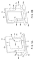
- FIG. 1A is an exemplary front view of a liquid crystal display television
- FIG. 1B is an exemplary side view of the liquid crystal display television
- FIG. 2 is an exemplary perspective view of the liquid crystal display television when seen from a direction of a stand;
- FIG. 3 is an exemplary exploded perspective view showing a television main body of the liquid crystal display television
- FIG. 4 is an exemplary perspective view showing a part of an LED module which constitutes a backlight
- FIG. 5 is an exemplary back view of a back chassis
- FIG. 6 is an exemplary back view of the back chassis holding a printed-circuit board which drives a liquid crystal cell;
- FIG. 7 is an exemplary back view of a third outer peripheral wall of the back chassis comprising a seat
- FIG. 8 is an exemplary back view showing a state in which first to fifth supporting members are arranged on the third outer peripheral wall of the back chassis;
- FIG. 9 is an exemplary back view showing a state in which the printed-circuit board is held on the third outer peripheral wall of the back chassis via the first to fifth supporting members;
- FIG. 10 is an exemplary cross sectional view taken along line F 10 -F 10 of FIG. 9 ;
- FIG. 11 is an exemplary cross sectional view taken along line F 11 -F 11 of FIG. 9 ;
- FIG. 12A is an exemplary perspective view of the first supporting member to be used in a first embodiment
- FIG. 12B is an exemplary perspective view of the first supporting member of FIG. 12A seen from the back;
- FIG. 13A is an exemplary perspective view of the second supporting member to be used in the first embodiment
- FIG. 13B is an exemplary perspective view of the second supporting member of FIG. 13A seen from the back;
- FIG. 14 is an exemplary perspective view showing a state in which the printed-circuit board is held on the third outer peripheral wall of the back chassis;
- FIG. 15 is an exemplary perspective view showing the third outer peripheral wall of the back chassis in which engagement holes are formed;
- FIG. 16 is an exemplary perspective view showing a state in which the second supporting member is arranged on the third outer peripheral wall of the back chassis;
- FIG. 17 is an exemplary perspective view showing a state in which the printed-circuit board is held on the third outer peripheral wall of the back chassis via the second supporting member;
- FIG. 18 is an exemplary plan view showing a positional relationship between engagement catches of the second supporting member and the engagement holes formed in the seat of the third outer peripheral wall;
- FIG. 19 is an exemplary perspective view showing a positional relationship between the engagement catches of the second supporting member and the engagement holes formed in the seat of the third outer peripheral wall;
- FIG. 20 is an exemplary perspective view of a second supporting member to be used in a second embodiment.
- an image display device comprises a light-emitting module, a housing comprising a back chassis covering the light-emitting module from behind and accommodating the light-emitting module, and a supporting member which is attached to an engagement hole formed in the back chassis and holds a circuit component on the back chassis.
- the supporting member comprises a receiving portion which receives the circuit component, and a light-shielding portion which is configured to block off light of the light-emitting module passing through the engagement hole in the back chassis.
- FIGS. 1A, 1B, and 2 disclose a liquid crystal display television 1 according to the first embodiment.
- the liquid crystal display television 1 is an example of a liquid crystal display device or an electronic device.
- the liquid crystal display television 1 comprises a stand 2 and a television main body 3 .
- the stand 2 is arranged on top board T of a television plinth, for example.
- the television main body 3 is supported by the stand 2 such that it stands on top board T.
- the television main body 3 comprises a housing 5 , a liquid crystal panel 6 , a backlight 7 , and a unit cover 8 as the main elements.
- the housing 5 includes a front bezel 10 made of resin, a metallic back chassis 11 , and a middle frame 12 made of resin.
- the front bezel 10 can be expressed in other words as a front cover or a first cover.
- the front bezel 10 is a horizontally long frame having first to fourth sides 13 a , 13 b , 13 c , and 13 d .
- the first side 13 a and the third side 13 c extend horizontally in a width direction of the television main body 3 , and are spaced apart from each other in a height direction of the television main body 3 and arranged in parallel to each other.
- the second side 13 b and the fourth side 13 d rise in the height direction of the television main body 3 , and are spaced apart from each other in the width direction of the television main body 3 and arranged in parallel to each other.
- the first to fourth sides 13 a , 13 b , 13 c , and 13 d define a rectangular opening 14 in cooperation with each other.
- the back chassis 11 can be expressed in other words as a back cover or a second cover.
- the back chassis 11 is combined with the front bezel 10 such that it covers the font bezel 10 from the behind.
- the back chassis 11 comprises a back wall 15 and first to fourth outer peripheral walls 16 a , 16 b , 16 c , and 16 d.
- the back wall 15 has a rectangular shape, and rises to face the opening 14 of the front bezel 10 .
- the stand 2 is fixed.
- the first to fourth outer peripheral walls 16 a , 16 b , 16 c , and 16 d are oriented toward the front bezel 10 from an outer periphery of the back wall 15 and inclined to protrude around back wall 15 . Front edge portions of the first to fourth outer peripheral walls 16 a , 16 b , 16 c , and 16 d are opposed to the first to fourth sides 13 a , 13 b , 13 c , and 13 d of the front bezel 10 , respectively.
- the middle frame 12 is a horizontally long frame having first to fourth sides 17 a , 17 b , 17 c , and 17 d .
- the first side 17 a is positioned between the first side 13 a of the front bezel 10 and the front edge portion of the first outer peripheral wall 16 a of the back chassis 11 .
- the second side 17 b is positioned between the second side 13 b of the front bezel 10 and the front edge portion of the second outer peripheral wall 16 b of the back chassis 11 .
- the third side 17 c is positioned between the third side 13 c of the front bezel 10 and the front edge portion of the third outer peripheral wall 16 c of the back chassis 11 .
- the fourth side 17 d is positioned between the fourth side 13 d of the front bezel 10 and the front edge portion of the fourth outer peripheral wall 16 d of the back chassis 11 .
- the first to fourth sides 17 a , 17 b , 17 c , and 17 d define a rectangular opening 18 in cooperation with each other.
- Each of the first to fourth sides 17 a , 17 b , 17 c , and 17 d of the middle frame 12 includes a flat support surface 20 as shown in FIGS. 10 and 11 .
- the flat support surfaces 20 of the first to fourth sides 17 a , 17 b , 17 c , and 17 d are contiguous along a periphery of the middle frame 12 to surround the opening 18 .
- the support surfaces 20 of the first to fourth sides 17 a , 17 b , 17 c , and 17 d are located on the same plane as each other and opposed to the front bezel 10 .
- the front bezel 10 , the back chassis 11 , and the middle frame 12 are coupled to each other via a plurality of metal clips or screws.
- the front bezel 10 , the back chassis 11 , and the middle frame 12 are assembled as an integrated construct and constitute the housing 5 which is flat and box-shaped.
- the liquid crystal panel 6 is accommodated inside the housing 5 .
- the liquid crystal panel 6 comprises a rectangular liquid crystal cell 22 , and two printed-circuit boards 23 a and 23 b equipped with a drive circuit for driving the liquid crystal cell 22 .
- the liquid crystal cell 22 comprises a screen 22 a for displaying an image.
- An outer peripheral portion of the liquid crystal cell 22 which is outside the screen 22 a is sandwiched between the front bezel 10 and the support surfaces 20 of the middle frame 12 . Accordingly, the screen 22 a of the liquid crystal cell 22 is exposed outside the housing 5 through the opening 14 .
- the printed-circuit boards 23 a and 23 b are an example of circuit components, and have an elongated figure extending in a width direction of the liquid crystal cell 22 . As shown in FIGS. 6 and 9 to 11 , the printed-circuit boards 23 a and 23 b are connected to a lower end portion of the liquid crystal cell 22 via a plurality of flexible printed wiring boards 24 . In the present embodiment, the flexible printed wiring boards 24 are folded back toward the back side of the liquid crystal cell 22 . Thereby, the printed-circuit boards 23 a and 23 b are positioned on the back surface of the third outer peripheral wall 16 c of the back chassis 11 .
- a diffusion plate 25 is arranged behind the liquid crystal cell 22 .
- the diffusion plate 25 is a rectangular plate having a size equal to the size of the liquid crystal cell 22 , and has a light diffusion property and a light transmission property.
- the diffusion plate 25 is interposed between the front edge portions of the first to fourth outer peripheral walls 16 a , 16 b , 16 c , and 16 d of the back chassis 11 and the middle frame 12 , and opposed to the opening 18 of the middle frame 12 .
- an optical sheet 26 is stacked on a front surface of the diffusion plate 25 .
- the optical sheet 26 includes, for example, three sheet elements 26 a , 26 b , and 26 c , such as a prism sheet or a light diffusion sheet.
- the optical sheet 26 faces the back surface of the liquid crystal cell 22 in the housing 5 . Between the optical sheet 26 and the back surface of the liquid crystal cell 22 , small clearance C is secured.
- the backlight 7 is accommodated in the housing 5 .
- the backlight 7 is an example of a light source, and comprises a plurality of LED modules 28 .
- each of the LED modules 28 comprises a module board 29 and a plurality of LEDs 30 .
- the module board 29 has an elongated shape extending in the width direction of the liquid crystal cell 22 .
- the LEDs 30 are mounted on a front surface of the module board 29 .
- the LEDs 30 are spaced apart from each other in a longitudinal direction of the module board 29 and aligned, and each of the LEDs 30 is covered by a lens 31 .
- the module board 29 is held on a front surface of the back wall 15 of the back chassis 11 .
- the lenses 31 covering the LEDs 30 face the diffusion plate 25 .
- the plurality of LED modules 28 are spaced apart from each other in a height direction of the liquid crystal cell 22 and arranged in parallel to each other. Further, the LED modules 28 are electrically connected to a printed-wiring board 32 supported on the back surface of the back wall 15 of the back chassis 11 .
- a white reflection sheet 33 is stacked on the front of the back chassis 11 .
- the reflection sheet 33 covers the front of the back chassis 11 and the module board 29 continuously.
- the lenses 31 covering the LEDs 30 pass through a plurality of through-holes 34 provided in the reflection sheet 33 to be exposed on the reflection sheet 33 .
- the reflection sheet 33 reflects the light incident on the back chassis 11 from the LEDs 30 onto the diffusion plate 25 .
- the reflected light is directed to the diffusion plate 25 together with the light directly incident on the diffusion plate 25 from the LEDs 30 .
- the light entering the diffusion plate 25 passes through the optical sheet 26 and impinges on the liquid crystal cell 22 . Consequently, the light is irradiated onto the liquid crystal cell 22 from the front surface of the diffusion plate 25 , and visibility of an image displayed on the screen 22 a of the liquid crystal cell 22 is enhanced.
- the liquid crystal panel 6 and the backlight 7 constitute a light-emitting module accommodated in the housing 5 .
- each of the printed-circuit boards 23 a and 23 b which drives the liquid crystal cell 22 is held on a back surface of the third outer peripheral wall 16 c positioned at a lower end portion of the back chassis 11 .
- the printed-circuit boards 23 a and 23 b are aligned in a width direction of the back chassis 11 .
- the printed-circuit board 23 a Since the structures for holding the printed-circuit boards 23 a and 23 b on the third outer peripheral wall 16 c are common to each other, one of the printed-circuit boards, i.e., the printed-circuit board 23 a , will be described as a typical example of the printed-circuit boards.
- a seat 35 is formed on the third outer peripheral wall 16 c of the back chassis 11 .
- the seat 35 protrudes downward from the third outer peripheral wall 16 c and extends linearly in the width direction of the back chassis 11 .
- the seat 35 includes a flat seating face 35 a exposed at the back of the back chassis 11 .
- the printed-circuit board 23 a is held on the seat 35 of the third outer peripheral wall 16 c via first to fifth supporting members 37 a , 37 b , 37 c , 37 d , and 37 e .
- the first to fifth supporting members 37 a , 37 b , 37 c , 37 d , and 37 e are made of a nonconductive synthetic resin material, for example, spaced apart from each other in a longitudinal direction of the printed-circuit board 23 a and aligned.
- the first, the third, and the fifth supporting members 37 a , 37 c , 37 e receive the printed-circuit board 23 a at both ends along a longitudinal direction of the printed-circuit board 23 a and an intermediate portion along the longitudinal direction of the printed-circuit board 23 a.
- the first supporting member 37 will be described as a typical example of the supporting members.
- the first supporting member 37 a comprises a receiving portion 38 for receiving the printed-circuit board 23 a .
- the receiving portion 38 is a rectangular frame structured by a pair of longitudinal bars 39 a and 39 b and a pair of lateral bars 40 a and 40 b , for example.
- the receiving portion 38 may be rephrased as a first portion.
- the longitudinal bars 39 a and 39 b are spaced apart from each other in the width direction of the back chassis 11 , and arranged in parallel to each other.
- One of the lateral bars i.e., the lateral bar 40 a
- the other one of the lateral bars i.e., the lateral bar 40 b
- the longitudinal bars 39 a and 39 b and the lateral bars 40 a and 40 b cooperate with each other and constitute a flat support surface 41 .
- the other one of the lateral bars i.e., the lateral bar 40 b comprises a wall 42 which receives a lower edge of the printed-circuit board 23 a .
- the wall 42 extends between the longitudinal bars 39 a and 39 b , and is projected further than the support surface 41 .
- the longitudinal bars 39 a and 39 b comprise engagement catches 43 a and 43 b .
- the engagement catches 43 a and 43 b are an example of an engagement portion, and are projected from the lower parts of the longitudinal bars 39 a and 39 b , respectively, toward the seat 35 of the third outer peripheral wall 16 c . Ends 44 a and 44 b of the engagement catches 43 a and 43 b are bent in direction in which they become distant from each other.
- the second supporting member 37 b receives the printed-circuit board 23 a between the first supporting member 37 a and the third supporting member 37 c , and also holds the printed-circuit board 23 a on the seating face 35 a .
- the fourth supporting member 37 d receives the printed-circuit board 23 a between the third supporting member 37 c and the fifth supporting member 37 e , and also holds the printed-circuit board 23 a on the seating face 35 a.
- the second and fourth supporting members 37 b and 37 d are different from the first, third and fifth supporting members 37 a , 37 c , and 37 e in that the second and fourth supporting members 37 b and 37 d each comprise a sandwiching piece 45 for retaining the printed-circuit board 23 a . Since structures other than the above have commonality with the structures of the first, third, and fifth supporting members 37 a , 37 c , and 37 e , the same reference numerals will be added to the common structural elements and their detailed explanations will be omitted.
- the sandwiching piece 45 is integrally formed with one of the lateral bars, i.e., the lateral bar 40 a .
- the sandwiching piece 45 is projected from an intermediate portion of one of the lateral bars, i.e., the lateral bar 40 a , toward the other lateral bar, i.e., the lateral bar 40 b , and positioned between the longitudinal bars 39 a and 39 b .
- the sandwiching piece 45 cooperates with the support surface 41 of the receiving portion 38 so that the printed-circuit board 23 a is sandwiched therebetween.
- the sandwiching piece 45 can be rephrased as a second portion.
- the sandwiching piece 45 resiliently contacts the printed-circuit board 23 a at a position of avoiding a plurality of circuit elements 51 , such as IC chips and connectors, and a conductive grounding gasket 52 mounted on the printed-circuit board 23 a.
- the printed-circuit board 23 a is sandwiched between the second and the fourth supporting members 37 b and 37 d and the support surface 41 , and at three places which are separated from each other in the longitudinal direction, the printed-circuit board 23 a is received by the first, the third, and the fifth supporting members 37 a , 37 c , and 37 e.
- engagement holes 46 a and 46 b into which the engagement catches 43 a and 43 b of each of the first to fifth supporting members 37 a , 37 b , 37 c , 37 d , and 37 e are fitted are formed.
- the engagement holes 46 a and 46 b are formed in the seating face 35 a of the seat 35 , and each of the engagement holes 46 a and 46 b is shaped as a rectangular opening.
- the engagement holes 46 a and 46 b are arranged to be spaced apart from each other in the width direction of the back chassis 11 .
- the seating face 35 a of the seat 35 includes five zones 47 , each including the engagement holes 46 a and 46 b aligned.
- the zones 47 are arranged to be spaced apart from each other in the width direction of the back chassis 11 .
- the engagement catches 43 a and 43 b of all of the supporting members 37 a , 37 b , 37 c , 37 d , and 37 e are inserted into the engagement holes 46 a and 46 b from the back of third outer peripheral wall 16 c .
- the ends 44 a and 44 b of the engagement catches 43 a and 43 b resiliently engage with opening edges of the engagement holes 46 a and 46 b .
- each of the supporting members 37 a , 37 b , 37 c , 37 d , and 37 e is mounted on the third outer peripheral wall 16 c such that it extends between the engagement holes 46 a and 46 b.
- an edge part on the opposite side of the support surface 41 of the longitudinal frames 39 a and 39 b abuts on the seating face 35 a of the seat 35 while the ends 44 a and 44 b of the engagement catches 43 a and 43 b is being engaged with the opening edges of the engagement holes 46 a and 46 b.
- vertically long gap g is formed between the engagement catch 43 a and the opening edge of the engagement hole 46 a , and between the engagement catch 43 b and the opening edge of the engagement hole 46 b .
- Gaps g are provided to allow insertion of the engagement catches 43 a and 43 b into the engagement holes 46 a and 46 b , and exposed outside the longitudinal bars 39 a and 39 b of the receiving portion 38 .
- the engagement holes 46 a and 46 b formed in the seating face 35 a of the seat 35 are covered by the printed-circuit board 23 a from the back of the back chassis 11 .
- FIGS. 12A, 12B, 13A and 13B illustrate the first supporting member 35 a and the second supporting member 35 b as typical examples of the supporting members
- all of the supporting members 37 a , 37 b , 37 c , 37 d , and 37 e comprise a pair of light-shielding walls 54 a and 54 b .
- the light-shielding walls 54 a and 54 b are an example of a light-shielding portion.
- the light-shielding walls 54 a and 54 b are projected in the width direction of the back chassis 11 from both ends of the other one of the lateral bars, i.e., the lateral bar 40 b , of the receiving portion 38 .
- the lateral bars 40 b protrude toward the third outer peripheral wall 16 c to be contiguous with the wall 42 .
- the other one of the lateral bars, i.e., the lateral bar 40 b , and the wall 42 connect between the light-shielding walls 54 a and 54 b.
- the light-shielding walls 54 a and 54 b protrude further outwardly along a direction in which the engagement holes 46 a and 46 b are arranged than each of the zones 47 on the seating face 35 a in which a pair of the engagement holes 46 a and 46 b are arranged. Accordingly, the light-shielding walls 54 a and 54 b are positioned directly below gaps g produced between the engagement catch 43 a and the opening edge of the engagement hole 46 a and between the engagement catch 43 b and the opening edge of the engagement hole 46 b , respectively. In addition to that, the light-shielding walls 54 a and 54 b are shaped to be larger than width dimensions of gaps g when the back chassis 11 is seen from the back.
- a pair of metallic shield boards 57 a and 57 b are fixed to the back wall 15 of the back chassis 11 by a plurality of screws.
- the shield boards 57 a and 57 b cover the printed-circuit boards 23 a and 23 b , respectively, from the back of the back chassis 11 , and are resiliently pressed against the grounding gaskets 52 mounted on their respective printed-circuit boards 23 a and 23 b.
- the printed-circuit boards 23 a and 23 b are pressed in a direction of approaching the third outer peripheral wall 16 c of the back chassis 11 by the shield boards 23 a and 23 b , and received by the receiving portions 38 of the first to fifth supporting members 37 a , 37 b , 37 c , 37 d , and 37 e .
- the receiving portions 38 are interposed between the third outer peripheral wall 16 c of the back chassis 11 and the printed-circuit boards 23 a and 23 b , and electrically insulate the third outer peripheral wall 16 c of the back chassis 11 from the printed-circuit boards 23 a and 23 b.
- FIGS. 10 and 11 As one of the shield boards, i.e., the shield board 57 a , is illustrated in FIGS. 10 and 11 as a typical example of the shield boards, a lower edge portion of the shield board 57 a is distant from the third outer peripheral wall 16 c of the back chassis 11 .
- a gap between the lower edge portion of the shield board 57 a and the front edge portion of the third outer peripheral wall 16 c is used as a path for passing the flexible printed wiring boards 24 therethrough. Consequently, the printed-circuit board 23 a held on the third outer peripheral wall 16 c is exposed at the lower side of the back chassis 11 from the gap between the lower edge portion of the shield board 57 a and the third outer peripheral wall 16 c.
- a front surface which faces the printed-circuit board 23 a is covered by a light reflection sheet 58 .
- the unit cover 8 is made of a synthetic resin material, for example.
- the unit cover 8 is assembled with the housing 5 in such a way that the back chassis 11 is covered from the back.
- the printed-circuit boards 23 and 23 b , the flexible printed wiring boards 24 , and the printed-wiring board 32 located behind the back chassis 11 are covered by the unit cover 8 . Accordingly, the unit cover 8 can be treated as a part of elements which constitute the housing 5 .
- the unit cover 8 comprises a lower wall 60 .
- the lower wall 60 is an example of a peripheral wall of the housing 5 , and covers a gap between the third outer peripheral wall 16 c of the back chassis 11 and the lower edge portions of the shield boards 57 a and 57 b from the bottom. Further, the lower wall 60 faces top board T of the television plinth.
- the lower wall 60 comprises a pair of openings 62 a and 62 b that emit sound produced by a pair of speakers 61 a and 61 b , and a plurality of air vents 63 for enhancing the heat discharge performance in the housing 5 .
- Each of the openings 62 a and 62 b and the air vents 63 is an example of a through-hole, and the openings 62 a and 62 b and the air vents 63 communicate with a region in which the printed-circuit boards 23 a and 23 b are held through the gap between the lower edge portions of the shield boards 57 a and 57 b and the third outer peripheral wall 16 c of the back chassis 11 .
- the light-shielding walls 54 a and 54 b of each of the first to fifth supporting members 37 a , 37 b , 37 c , 37 d , and 37 e are projected from the receiving portion 38 of each of the first to fifth supporting members 37 a , 37 b , 37 c , 37 d , and 37 e such that they thrust into space between the lower wall 60 of the unit cover 8 and gaps g, which are formed between the engagement catch 43 a and the opening edge of the engagement hole 46 a and between the engagement catch 43 b and the opening edge of the engagement hole 46 b , respectively.
- a plurality of engagement holes 46 a and 46 b for arranging the first to fifth supporting members 37 a , 37 b , 37 c , 37 d , and 37 e are formed. For this reason, it is possible that a part of light emitted by the LED modules 28 will leak to the back and the bottom of the back chassis 11 through the engagement holes 46 a and 46 b.
- the engagement holes 46 a and 46 b are covered from the back of the back chassis 11 by the printed-circuit boards 23 a and 23 b received by the receiving portions 38 of the first to fifth supporting members 37 a , 37 b , 37 c , 37 d , and 38 e .
- the light-shielding walls 54 a and 54 b formed integrally with the receiving portions 38 are positioned directly below gaps g formed between the engagement catch 43 a and the engagement hole 46 a and between the engagement catch 43 b and the engagement hole 46 b , respectively.
- the light directed toward the back of the back chassis 11 passing through the engagement holes 46 a and 46 b is blocked off by the printed-circuit boards 23 a and 23 b .
- the light directed toward the lower part of the back chassis 11 which comes out through the gaps g is blocked off by the light-shielding walls 54 a and 54 b.
- the light emitted from the LED modules 28 can be prevented from leaking from engagement holes 46 a and 46 b of the back chassis 11 .
- the openings 62 a and 62 b for emitting sound and the air vents 63 a are provided in the lower wall 60 of the unit cover 8 , it is possible to prevent the light from leaking from here.
- the first to fifth supporting members 37 a , 37 b , 37 c , 37 d , and 37 e can be held on the back chassis 11 by mere mechanical engagement, and the workability in assembling the liquid crystal television 1 can be improved.
- FIG. 20 discloses a second embodiment.
- the second embodiment is different from the first embodiment in that the form of a receiving portion 38 of each of first to fifth supporting members 37 a , 37 b , 37 c , 37 d , and 37 e is different, and structures other than the above are similar to those of the first embodiment.
- a second supporting member 37 b will be described as a typical example of the supporting members.
- a wall 42 of the second supporting member 37 b is cut out between a longitudinal bar 39 a and a longitudinal bar 39 b . That is, a recessed portion 71 indented toward a lateral bar 40 b is formed in the wall 42 . In the presence of the recessed portion 71 , the wall 42 which contacts lower edges of printed-circuit boards 23 a and 23 b is separated into a first end portion 72 a and a second end portion 72 b .
- the first end portion 72 a is contiguous with one of light-shielding walls, i.e., a light-shielding wall 54 a
- the second end portion 72 b is contiguous with the other light-shielding wall, i.e., a light-shielding wall 54 b.
- the sandwiching piece 45 for sandwiching each of the printed-circuit boards 23 a and 23 b is provided for only the second and the fourth supporting members 37 b and 37 d .
- elements for which such a sandwiching piece is provided are not limited to above.
- a similar sandwiching piece 45 may be provided for the first, third, and fifth supporting members 37 a , 37 c , and 37 e as well, so that the printed-circuit boards 23 a and 23 b are held by all of the supporting members 37 a , 37 b , 37 c , 37 d , and 37 e.
- a circuit component to be held on a back chassis is not specified to a printed-circuit board, and may be a wire harness of bundled cables, for example.
Landscapes
- Physics & Mathematics (AREA)
- Nonlinear Science (AREA)
- Mathematical Physics (AREA)
- Chemical & Material Sciences (AREA)
- Crystallography & Structural Chemistry (AREA)
- General Physics & Mathematics (AREA)
- Optics & Photonics (AREA)
- Liquid Crystal (AREA)
- Devices For Indicating Variable Information By Combining Individual Elements (AREA)
Abstract
Description
Claims (12)
Applications Claiming Priority (2)
| Application Number | Priority Date | Filing Date | Title |
|---|---|---|---|
| JP2013203463A JP2015069016A (en) | 2013-09-30 | 2013-09-30 | Video display device |
| JP2013-203463 | 2013-09-30 |
Publications (2)
| Publication Number | Publication Date |
|---|---|
| US20150092394A1 US20150092394A1 (en) | 2015-04-02 |
| US9535286B2 true US9535286B2 (en) | 2017-01-03 |
Family
ID=50336065
Family Applications (1)
| Application Number | Title | Priority Date | Filing Date |
|---|---|---|---|
| US14/225,200 Active 2034-11-24 US9535286B2 (en) | 2013-09-30 | 2014-03-25 | Image display device |
Country Status (3)
| Country | Link |
|---|---|
| US (1) | US9535286B2 (en) |
| EP (1) | EP2853938A1 (en) |
| JP (1) | JP2015069016A (en) |
Families Citing this family (4)
| Publication number | Priority date | Publication date | Assignee | Title |
|---|---|---|---|---|
| EP3264400B1 (en) * | 2015-02-23 | 2020-05-20 | Panasonic Intellectual Property Management Co., Ltd. | Back plate for use in a display device and display device comprising such a back plate |
| CN105158974B (en) * | 2015-09-29 | 2019-03-19 | 惠州Tcl移动通信有限公司 | A kind of backlight module and the mobile device with the backlight module |
| KR102411320B1 (en) * | 2017-08-31 | 2022-06-22 | 엘지디스플레이 주식회사 | Display device |
| KR102784504B1 (en) * | 2019-07-17 | 2025-03-21 | 엘지전자 주식회사 | Display device |
Citations (12)
| Publication number | Priority date | Publication date | Assignee | Title |
|---|---|---|---|---|
| US5313318A (en) * | 1991-11-04 | 1994-05-17 | Apple Computer, Inc. | Internal frame for a liquid crystal display not extending to the upper surface thereof, light guide and circuitry assembly |
| US6342932B1 (en) * | 1998-11-12 | 2002-01-29 | Matshushita Electric Industrial Co., Ltd. | Liquid crystal display |
| US6411352B1 (en) | 1998-08-10 | 2002-06-25 | Lg. Philips Lcd Co., Ltd. | Slim liquid crystal display device |
| US20020186333A1 (en) * | 2001-05-07 | 2002-12-12 | Jin-Ho Ha | Liquid crystal display device and method for assembling the same |
| US20050068261A1 (en) * | 2003-08-12 | 2005-03-31 | Se-Il Oh | Plasma display device |
| US20100188598A1 (en) | 2009-01-28 | 2010-07-29 | Funai Electric Co., Ltd. | Liquid crystal module |
| US20120092584A1 (en) | 2010-10-13 | 2012-04-19 | Samsung Electronics Co., Ltd. | Liquid crystal display module and liquid crystal display device having the same |
| US20130033658A1 (en) | 2011-08-04 | 2013-02-07 | Panasonic Liquid Crystal Display Co., Ltd. | Liquid crystal display device |
| US8437120B2 (en) * | 2009-11-17 | 2013-05-07 | Samsung Electronics Co., Ltd. | Image display device |
| JP2013130831A (en) | 2011-12-22 | 2013-07-04 | Sharp Corp | Display device and television receiver |
| US8988867B2 (en) * | 2010-06-24 | 2015-03-24 | Sharp Kabushiki Kaisha | Display device and television receiver |
| US9013887B2 (en) * | 2011-07-29 | 2015-04-21 | Wistron Corporation | Display device |
-
2013
- 2013-09-30 JP JP2013203463A patent/JP2015069016A/en active Pending
-
2014
- 2014-03-10 EP EP14158462.3A patent/EP2853938A1/en not_active Withdrawn
- 2014-03-25 US US14/225,200 patent/US9535286B2/en active Active
Patent Citations (13)
| Publication number | Priority date | Publication date | Assignee | Title |
|---|---|---|---|---|
| US5313318A (en) * | 1991-11-04 | 1994-05-17 | Apple Computer, Inc. | Internal frame for a liquid crystal display not extending to the upper surface thereof, light guide and circuitry assembly |
| US6411352B1 (en) | 1998-08-10 | 2002-06-25 | Lg. Philips Lcd Co., Ltd. | Slim liquid crystal display device |
| US6342932B1 (en) * | 1998-11-12 | 2002-01-29 | Matshushita Electric Industrial Co., Ltd. | Liquid crystal display |
| US20020186333A1 (en) * | 2001-05-07 | 2002-12-12 | Jin-Ho Ha | Liquid crystal display device and method for assembling the same |
| US20050068261A1 (en) * | 2003-08-12 | 2005-03-31 | Se-Il Oh | Plasma display device |
| JP2010175704A (en) | 2009-01-28 | 2010-08-12 | Funai Electric Co Ltd | Liquid crystal module |
| US20100188598A1 (en) | 2009-01-28 | 2010-07-29 | Funai Electric Co., Ltd. | Liquid crystal module |
| US8437120B2 (en) * | 2009-11-17 | 2013-05-07 | Samsung Electronics Co., Ltd. | Image display device |
| US8988867B2 (en) * | 2010-06-24 | 2015-03-24 | Sharp Kabushiki Kaisha | Display device and television receiver |
| US20120092584A1 (en) | 2010-10-13 | 2012-04-19 | Samsung Electronics Co., Ltd. | Liquid crystal display module and liquid crystal display device having the same |
| US9013887B2 (en) * | 2011-07-29 | 2015-04-21 | Wistron Corporation | Display device |
| US20130033658A1 (en) | 2011-08-04 | 2013-02-07 | Panasonic Liquid Crystal Display Co., Ltd. | Liquid crystal display device |
| JP2013130831A (en) | 2011-12-22 | 2013-07-04 | Sharp Corp | Display device and television receiver |
Non-Patent Citations (1)
| Title |
|---|
| European Application No./Patent No. 14158462.3; Extended European Search Report; Mailed Feb. 17, 2015. |
Also Published As
| Publication number | Publication date |
|---|---|
| US20150092394A1 (en) | 2015-04-02 |
| JP2015069016A (en) | 2015-04-13 |
| EP2853938A1 (en) | 2015-04-01 |
Similar Documents
| Publication | Publication Date | Title |
|---|---|---|
| US9810832B2 (en) | Illumination device, display device, and television receiving device | |
| EP2913816B1 (en) | Display device | |
| US10036848B2 (en) | Lighting device, display device, and television device | |
| WO2014196228A1 (en) | Illumination device, display device, and tv receiver | |
| CN104412314B (en) | Display device and radiovisor | |
| WO2012014601A1 (en) | Illumination apparatus, display apparatus, and television receiver apparatus | |
| WO2011148733A1 (en) | Lighting device, display device, and television receiving device | |
| JP4212062B1 (en) | LCD panel | |
| CN104471305A (en) | Lighting device, display device and television receiving device | |
| US9535286B2 (en) | Image display device | |
| WO2014073425A1 (en) | Illumination device, display device, and television receiver device | |
| EP2720080A1 (en) | Liquid crystal display in which a light source is accommodated in a through-hole in the supporting frame of the backlight for cooling purposes | |
| WO2013191051A1 (en) | Display, and television receiver | |
| JP5367867B2 (en) | Liquid crystal display device and television receiver | |
| CN104040413B (en) | Display device and radiovisor | |
| WO2011089960A1 (en) | Lighting device, display device, and television receiver device | |
| JP2014074756A (en) | Display device and television receiver | |
| US20160131828A1 (en) | Illumination device, display device, and tv receiver | |
| JP5677996B2 (en) | Display device and television receiver | |
| WO2014141882A1 (en) | Display apparatus and television receiving apparatus | |
| WO2014181566A1 (en) | Lighting device, display device, and television receiving device | |
| JP2008243558A (en) | Backlight device | |
| WO2014010522A1 (en) | Display device and television receiver | |
| JP2014077927A (en) | Television and electronic equipment | |
| WO2013191047A1 (en) | Display, and television receiver |
Legal Events
| Date | Code | Title | Description |
|---|---|---|---|
| AS | Assignment |
Owner name: KABUSHIKI KAISHA TOSHIBA, JAPAN Free format text: ASSIGNMENT OF ASSIGNORS INTEREST;ASSIGNOR:SAKURADA, HIROKI;REEL/FRAME:032527/0210 Effective date: 20140314 |
|
| AS | Assignment |
Owner name: TOSHIBA VISUAL SOLUTIONS CORPORATION, JAPAN Free format text: NUNC PRO TUNC ASSIGNMENT;ASSIGNOR:TOSHIBA LIFESTYLE PRODUCTS & SERVICES CORPORATION;REEL/FRAME:040412/0960 Effective date: 20160630 Owner name: TOSHIBA LIFESTYLE PRODUCTS & SERVICES CORPORATION, Free format text: NUNC PRO TUNC ASSIGNMENT;ASSIGNOR:KABUSHIKI KAISHA TOSHIBA;REEL/FRAME:040412/0920 Effective date: 20160630 |
|
| STCF | Information on status: patent grant |
Free format text: PATENTED CASE |
|
| AS | Assignment |
Owner name: TOSHIBA LIFESTYLE PRODUCTS & SERVICES CORPORATION, Free format text: NUNC PRO TUNC ASSIGNMENT;ASSIGNOR:KABUSHIKI KAISHA TOSHIBA;REEL/FRAME:041009/0193 Effective date: 20160630 Owner name: TOSHIBA VISUAL SOLUTIONS CORPORATION, JAPAN Free format text: NUNC PRO TUNC ASSIGNMENT;ASSIGNOR:TOSHIBA LIFESTYLE PRODUCTS & SERVICES CORPORATION;REEL/FRAME:041010/0031 Effective date: 20160630 |
|
| AS | Assignment |
Owner name: TOSHIBA VISUAL SOLUTIONS CORPORATION, JAPAN Free format text: ASSIGNMENT OF ASSIGNORS INTEREST;ASSIGNOR:KABUSHIKI KAISHA TOSHIBA;REEL/FRAME:046881/0120 Effective date: 20180420 |
|
| AS | Assignment |
Owner name: HISENSE VISUAL TECHNOLOGY CO., LTD., CHINA Free format text: ASSIGNMENT OF ASSIGNORS INTEREST;ASSIGNOR:TOSHIBA VISUAL SOLUTIONS CORPORATION;REEL/FRAME:051493/0333 Effective date: 20191225 |
|
| MAFP | Maintenance fee payment |
Free format text: PAYMENT OF MAINTENANCE FEE, 4TH YEAR, LARGE ENTITY (ORIGINAL EVENT CODE: M1551); ENTITY STATUS OF PATENT OWNER: LARGE ENTITY Year of fee payment: 4 |