US9533370B2 - Method for laser marking an anodized metal surface with a desired colour - Google Patents
Method for laser marking an anodized metal surface with a desired colour Download PDFInfo
- Publication number
- US9533370B2 US9533370B2 US15/036,967 US201415036967A US9533370B2 US 9533370 B2 US9533370 B2 US 9533370B2 US 201415036967 A US201415036967 A US 201415036967A US 9533370 B2 US9533370 B2 US 9533370B2
- Authority
- US
- United States
- Prior art keywords
- laser
- pulse
- spot
- scanner
- scanning
- Prior art date
- Legal status (The legal status is an assumption and is not a legal conclusion. Google has not performed a legal analysis and makes no representation as to the accuracy of the status listed.)
- Active
Links
- 238000000034 method Methods 0.000 title claims abstract description 58
- 229910052751 metal Inorganic materials 0.000 title claims abstract description 47
- 239000002184 metal Substances 0.000 title claims abstract description 47
- 238000010330 laser marking Methods 0.000 title claims abstract description 14
- 238000000926 separation method Methods 0.000 claims abstract description 23
- 238000002048 anodisation reaction Methods 0.000 claims description 31
- 229910000838 Al alloy Inorganic materials 0.000 claims description 5
- 239000011324 bead Substances 0.000 claims description 5
- 239000011521 glass Substances 0.000 claims description 5
- 238000001556 precipitation Methods 0.000 claims description 5
- 241000872198 Serjania polyphylla Species 0.000 claims description 2
- 238000012545 processing Methods 0.000 description 11
- 239000004411 aluminium Substances 0.000 description 9
- 229910052782 aluminium Inorganic materials 0.000 description 9
- XAGFODPZIPBFFR-UHFFFAOYSA-N aluminium Chemical compound [Al] XAGFODPZIPBFFR-UHFFFAOYSA-N 0.000 description 9
- 230000003287 optical effect Effects 0.000 description 9
- 239000000463 material Substances 0.000 description 8
- 239000000975 dye Substances 0.000 description 6
- 230000000694 effects Effects 0.000 description 6
- 239000000126 substance Substances 0.000 description 5
- 230000003685 thermal hair damage Effects 0.000 description 5
- 230000006378 damage Effects 0.000 description 4
- 239000000835 fiber Substances 0.000 description 4
- 239000000976 ink Substances 0.000 description 4
- 230000008569 process Effects 0.000 description 4
- 238000002679 ablation Methods 0.000 description 3
- 230000008901 benefit Effects 0.000 description 3
- 238000005336 cracking Methods 0.000 description 3
- 150000002739 metals Chemical class 0.000 description 3
- CURLTUGMZLYLDI-UHFFFAOYSA-N Carbon dioxide Chemical compound O=C=O CURLTUGMZLYLDI-UHFFFAOYSA-N 0.000 description 2
- FYYHWMGAXLPEAU-UHFFFAOYSA-N Magnesium Chemical compound [Mg] FYYHWMGAXLPEAU-UHFFFAOYSA-N 0.000 description 2
- RTAQQCXQSZGOHL-UHFFFAOYSA-N Titanium Chemical compound [Ti] RTAQQCXQSZGOHL-UHFFFAOYSA-N 0.000 description 2
- HCHKCACWOHOZIP-UHFFFAOYSA-N Zinc Chemical compound [Zn] HCHKCACWOHOZIP-UHFFFAOYSA-N 0.000 description 2
- 238000013459 approach Methods 0.000 description 2
- 230000008859 change Effects 0.000 description 2
- 230000006835 compression Effects 0.000 description 2
- 238000007906 compression Methods 0.000 description 2
- 230000001934 delay Effects 0.000 description 2
- 238000002474 experimental method Methods 0.000 description 2
- 239000011777 magnesium Substances 0.000 description 2
- 229910052749 magnesium Inorganic materials 0.000 description 2
- 229910052758 niobium Inorganic materials 0.000 description 2
- 239000010955 niobium Substances 0.000 description 2
- GUCVJGMIXFAOAE-UHFFFAOYSA-N niobium atom Chemical compound [Nb] GUCVJGMIXFAOAE-UHFFFAOYSA-N 0.000 description 2
- 239000013307 optical fiber Substances 0.000 description 2
- 239000007787 solid Substances 0.000 description 2
- 229910052715 tantalum Inorganic materials 0.000 description 2
- GUVRBAGPIYLISA-UHFFFAOYSA-N tantalum atom Chemical compound [Ta] GUVRBAGPIYLISA-UHFFFAOYSA-N 0.000 description 2
- 229910052719 titanium Inorganic materials 0.000 description 2
- 239000010936 titanium Substances 0.000 description 2
- 229910052725 zinc Inorganic materials 0.000 description 2
- 239000011701 zinc Substances 0.000 description 2
- 238000010521 absorption reaction Methods 0.000 description 1
- 238000007743 anodising Methods 0.000 description 1
- 238000005422 blasting Methods 0.000 description 1
- 229910002092 carbon dioxide Inorganic materials 0.000 description 1
- 239000001569 carbon dioxide Substances 0.000 description 1
- 238000004140 cleaning Methods 0.000 description 1
- 239000003086 colorant Substances 0.000 description 1
- 238000004737 colorimetric analysis Methods 0.000 description 1
- 238000001914 filtration Methods 0.000 description 1
- 230000012447 hatching Effects 0.000 description 1
- 230000006872 improvement Effects 0.000 description 1
- 238000004519 manufacturing process Methods 0.000 description 1
- 238000012986 modification Methods 0.000 description 1
- 230000004048 modification Effects 0.000 description 1
- 238000005498 polishing Methods 0.000 description 1
- 229910052761 rare earth metal Inorganic materials 0.000 description 1
- 150000002910 rare earth metals Chemical class 0.000 description 1
- 230000000717 retained effect Effects 0.000 description 1
- 230000002441 reversible effect Effects 0.000 description 1
- 239000000758 substrate Substances 0.000 description 1
- 230000002123 temporal effect Effects 0.000 description 1
Images


Classifications
-
- B—PERFORMING OPERATIONS; TRANSPORTING
- B23—MACHINE TOOLS; METAL-WORKING NOT OTHERWISE PROVIDED FOR
- B23K—SOLDERING OR UNSOLDERING; WELDING; CLADDING OR PLATING BY SOLDERING OR WELDING; CUTTING BY APPLYING HEAT LOCALLY, e.g. FLAME CUTTING; WORKING BY LASER BEAM
- B23K26/00—Working by laser beam, e.g. welding, cutting or boring
- B23K26/50—Working by transmitting the laser beam through or within the workpiece
- B23K26/57—Working by transmitting the laser beam through or within the workpiece the laser beam entering a face of the workpiece from which it is transmitted through the workpiece material to work on a different workpiece face, e.g. for effecting removal, fusion splicing, modifying or reforming
-
- B23K26/0063—
-
- B—PERFORMING OPERATIONS; TRANSPORTING
- B23—MACHINE TOOLS; METAL-WORKING NOT OTHERWISE PROVIDED FOR
- B23K—SOLDERING OR UNSOLDERING; WELDING; CLADDING OR PLATING BY SOLDERING OR WELDING; CUTTING BY APPLYING HEAT LOCALLY, e.g. FLAME CUTTING; WORKING BY LASER BEAM
- B23K26/00—Working by laser beam, e.g. welding, cutting or boring
- B23K26/0006—Working by laser beam, e.g. welding, cutting or boring taking account of the properties of the material involved
-
- B—PERFORMING OPERATIONS; TRANSPORTING
- B23—MACHINE TOOLS; METAL-WORKING NOT OTHERWISE PROVIDED FOR
- B23K—SOLDERING OR UNSOLDERING; WELDING; CLADDING OR PLATING BY SOLDERING OR WELDING; CUTTING BY APPLYING HEAT LOCALLY, e.g. FLAME CUTTING; WORKING BY LASER BEAM
- B23K26/00—Working by laser beam, e.g. welding, cutting or boring
- B23K26/02—Positioning or observing the workpiece, e.g. with respect to the point of impact; Aligning, aiming or focusing the laser beam
- B23K26/06—Shaping the laser beam, e.g. by masks or multi-focusing
- B23K26/062—Shaping the laser beam, e.g. by masks or multi-focusing by direct control of the laser beam
- B23K26/0622—Shaping the laser beam, e.g. by masks or multi-focusing by direct control of the laser beam by shaping pulses
-
- B—PERFORMING OPERATIONS; TRANSPORTING
- B23—MACHINE TOOLS; METAL-WORKING NOT OTHERWISE PROVIDED FOR
- B23K—SOLDERING OR UNSOLDERING; WELDING; CLADDING OR PLATING BY SOLDERING OR WELDING; CUTTING BY APPLYING HEAT LOCALLY, e.g. FLAME CUTTING; WORKING BY LASER BEAM
- B23K26/00—Working by laser beam, e.g. welding, cutting or boring
- B23K26/02—Positioning or observing the workpiece, e.g. with respect to the point of impact; Aligning, aiming or focusing the laser beam
- B23K26/06—Shaping the laser beam, e.g. by masks or multi-focusing
- B23K26/064—Shaping the laser beam, e.g. by masks or multi-focusing by means of optical elements, e.g. lenses, mirrors or prisms
- B23K26/0643—Shaping the laser beam, e.g. by masks or multi-focusing by means of optical elements, e.g. lenses, mirrors or prisms comprising mirrors
-
- B—PERFORMING OPERATIONS; TRANSPORTING
- B23—MACHINE TOOLS; METAL-WORKING NOT OTHERWISE PROVIDED FOR
- B23K—SOLDERING OR UNSOLDERING; WELDING; CLADDING OR PLATING BY SOLDERING OR WELDING; CUTTING BY APPLYING HEAT LOCALLY, e.g. FLAME CUTTING; WORKING BY LASER BEAM
- B23K26/00—Working by laser beam, e.g. welding, cutting or boring
- B23K26/02—Positioning or observing the workpiece, e.g. with respect to the point of impact; Aligning, aiming or focusing the laser beam
- B23K26/06—Shaping the laser beam, e.g. by masks or multi-focusing
- B23K26/064—Shaping the laser beam, e.g. by masks or multi-focusing by means of optical elements, e.g. lenses, mirrors or prisms
- B23K26/0648—Shaping the laser beam, e.g. by masks or multi-focusing by means of optical elements, e.g. lenses, mirrors or prisms comprising lenses
-
- B—PERFORMING OPERATIONS; TRANSPORTING
- B23—MACHINE TOOLS; METAL-WORKING NOT OTHERWISE PROVIDED FOR
- B23K—SOLDERING OR UNSOLDERING; WELDING; CLADDING OR PLATING BY SOLDERING OR WELDING; CUTTING BY APPLYING HEAT LOCALLY, e.g. FLAME CUTTING; WORKING BY LASER BEAM
- B23K26/00—Working by laser beam, e.g. welding, cutting or boring
- B23K26/08—Devices involving relative movement between laser beam and workpiece
- B23K26/082—Scanning systems, i.e. devices involving movement of the laser beam relative to the laser head
-
- B—PERFORMING OPERATIONS; TRANSPORTING
- B41—PRINTING; LINING MACHINES; TYPEWRITERS; STAMPS
- B41J—TYPEWRITERS; SELECTIVE PRINTING MECHANISMS, i.e. MECHANISMS PRINTING OTHERWISE THAN FROM A FORME; CORRECTION OF TYPOGRAPHICAL ERRORS
- B41J2/00—Typewriters or selective printing mechanisms characterised by the printing or marking process for which they are designed
- B41J2/435—Typewriters or selective printing mechanisms characterised by the printing or marking process for which they are designed characterised by selective application of radiation to a printing material or impression-transfer material
- B41J2/44—Typewriters or selective printing mechanisms characterised by the printing or marking process for which they are designed characterised by selective application of radiation to a printing material or impression-transfer material using single radiation source per colour, e.g. lighting beams or shutter arrangements
- B41J2/442—Typewriters or selective printing mechanisms characterised by the printing or marking process for which they are designed characterised by selective application of radiation to a printing material or impression-transfer material using single radiation source per colour, e.g. lighting beams or shutter arrangements using lasers
-
- B—PERFORMING OPERATIONS; TRANSPORTING
- B41—PRINTING; LINING MACHINES; TYPEWRITERS; STAMPS
- B41J—TYPEWRITERS; SELECTIVE PRINTING MECHANISMS, i.e. MECHANISMS PRINTING OTHERWISE THAN FROM A FORME; CORRECTION OF TYPOGRAPHICAL ERRORS
- B41J3/00—Typewriters or selective printing or marking mechanisms characterised by the purpose for which they are constructed
- B41J3/407—Typewriters or selective printing or marking mechanisms characterised by the purpose for which they are constructed for marking on special material
- B41J3/413—Typewriters or selective printing or marking mechanisms characterised by the purpose for which they are constructed for marking on special material for metal
-
- B—PERFORMING OPERATIONS; TRANSPORTING
- B41—PRINTING; LINING MACHINES; TYPEWRITERS; STAMPS
- B41M—PRINTING, DUPLICATING, MARKING, OR COPYING PROCESSES; COLOUR PRINTING
- B41M5/00—Duplicating or marking methods; Sheet materials for use therein
- B41M5/0041—Digital printing on surfaces other than ordinary paper
- B41M5/0058—Digital printing on surfaces other than ordinary paper on metals and oxidised metal surfaces
-
- B—PERFORMING OPERATIONS; TRANSPORTING
- B41—PRINTING; LINING MACHINES; TYPEWRITERS; STAMPS
- B41M—PRINTING, DUPLICATING, MARKING, OR COPYING PROCESSES; COLOUR PRINTING
- B41M5/00—Duplicating or marking methods; Sheet materials for use therein
- B41M5/26—Thermography ; Marking by high energetic means, e.g. laser otherwise than by burning, and characterised by the material used
- B41M5/262—Thermography ; Marking by high energetic means, e.g. laser otherwise than by burning, and characterised by the material used recording or marking of inorganic surfaces or materials, e.g. glass, metal, or ceramics
Definitions
- This invention relates to a method for laser marking an anodized metal surface with a desired color.
- the invention has particular application for rapidly marking anodized aluminium consumer goods with high quality black marks without the use of dyes, inks or other chemicals.
- Laser marking has been applied to many materials including metals. Once perfected for a particular material, the laser marking process is typically reliable, repeatable, and amenable to high-throughput high-yield production.
- An example is the color marking of anodized aluminium, a material that is in widespread use as it is lightweight, strong, easily shaped, and has a durable surface finish.
- the anodized surface is generally dyed with colored dyes.
- Laser light can be used directly to form various colors either within the anodization or in the interface region between the oxide layer that forms the anodization and the aluminium. Similar marks can also be made on other anodized metal surfaces such as titanium, zinc, magnesium, niobium and tantalum.
- U.S. Pat. No. 6,777,098 describes a method of marking anodized aluminium articles with black marks which occur in a layer between the anodization and the aluminium and therefore are as durable as the anodized surface.
- the marks described therein are described as being dark grey or black in hue and somewhat less shiny than unmarked portion using nanosecond range infrared laser pulses.
- 6,777,098 are disadvantageous because (i) creating commercially desirable black marks with nanosecond range pulses tends to cause destruction of the oxide layer, and (ii) cleaning of the aluminium following polishing or other processing adds another step in the process, with associated expense, and possibly disturbs a desired surface finish.
- U.S. Pat. No. 8,451,873 discloses a method for creating a mark on an anodized specimen. The method involves providing a laser marking system having controllable laser pulse parameters, determining the laser pulse parameters associated with the desired properties, and directing the laser marking system to mark the article using the selected laser pulse parameters. Laser marks so made have an optical density that ranges from transparent to opaque, a white color, a texture indistinguishable from the surrounding article, and durable, substantially intact anodization. The patent teaches that marks created using laser pulses greater than 1 nanosecond results in clear signs of cracking of the anodization.
- the patent teaches that when marking with prior art nanosecond pulses, applying enough laser pulse energy to the surface to make dark marks causes damage to the anodization which causes the appearance of the marks to change with viewing angle.
- the patent also teaches solving this problem by using pulses having pulse widths of approximately 10 ps. Marks produced by using pulses having pulse widths of approximately 10 ps or less do not damage the anodization, regardless of how dark the marks are, and nor do the marks change in appearance with viewing angle.
- Such marks are typical of so-called “cold processing” that utilize multi-photon absorption effects in the material. Cold processing (such as cold ablation) does not rely on thermal effects to produce the desired processing effect, and therefore has little if any thermal damage surrounding the processed area.
- femtosecond lasers or picosecond lasers having pulse widths up to around 10 ps to 50 ps.
- the picosecond lasers used in the patent were much less expensive than femtosecond lasers, the picosecond lasers users are more expensive than nanosecond lasers because they rely on very advanced techniques and components such as optical pulse compressors to produce the very narrow laser pulse widths.
- an L value lower than approximately 30 is more commercially important, and for this, the picosecond lasers used do not write the marks quickly enough for many commercial applications where cost is at a premium. It is advantageous not to rely on expensive techniques or components such as optical pulse compression and optical pulse compressors.
- a method for laser marking an anodized metal surface with a desired color comprises: providing a laser for emitting a laser beam comprising laser pulses having a pulse energy, a pulse width, and a pulse repetition frequency; providing a scanner comprising a first mirror for scanning the laser beam in a first direction, and a second mirror for scanning the laser beam in a second direction; providing a lens for focussing the laser beam from the laser onto the anodized metal surface to form a spot having a spot diameter and a pulse fluence; providing a controller for controlling the scanner with a control signal; marking a plurality of lines separated by a hatch distance on the anodized metal surface to form a desired mark by scanning the scanner while pulsing the laser; and selecting a scan speed, the pulse repetition frequency, and the spot diameter such that the separation between consecutive spots during each scan of the scanner is at least one quarter of the spot diameter; the method being characterized by overwriting each line more than once,
- the method of the present invention is particularly attractive because it is able to produce marks on anodized metal surfaces faster, and therefore more economically, than has hitherto been possible.
- a black mark can be obtained with lines that are written only once, with spot to spot separations of approximately 10 ⁇ m and line to line spacings (hatching) of approximately 0.2 ⁇ m.
- Considerable time will be spent between scans when using a typical scanner with a “digital” resolution of 2 ⁇ m as a relatively complicated waveform needs to be derived to control the scanner to achieve a sub-digital resolution of 0.2 ⁇ m.
- Each line may be written by scanning the first mirror while holding the second mirror stationary.
- Other ways of writing the lines may be employed, for example the angular position of the second mirror can be incremented in proportion to the angular position of the first mirror. However this is not preferred.
- the hatch distance may be achieved by moving the second mirror.
- the second mirror may be characterized by a digital resolution, and the hatch distance may correspond to an integral multiple of the digital resolution.
- the metal may be a precipitation hardened aluminium alloy.
- Other metals may be employed, for example anodized titanium, zinc, magnesium, niobium and tantalum.
- the metal may have been glass bead blasted.
- the metal may have been hard anodized.
- the anodization may have a thickness between 5 ⁇ m and 25 ⁇ m.
- the thickness may be between 5 ⁇ m and 15 ⁇ m.
- the anodization may be clear. Alternatively or additionally, the anodization may be colored.
- the color may be any suitable color, for example black or gray.
- black or gray When the color is black, then a black mark that can be written rapidly onto consumer goods having near perfect finishes. This is commercially very important and indeed it can make the difference between the mark being commercially viable or non-viable.
- the color may be gray or black with an L value no greater than 40.
- the L value is no greater than 30.
- a mark with an L value no greater than 30 would generally be considered to be a black mark.
- the laser may be a pulsed laser providing a laser beam having a pulse width greater than one hundred picoseconds.
- the scanner may be accelerated prior to pulsing the laser. This step reduces edge effects by ensuring that the scanner is already moving at its desired speed when the laser is first turned on during each scan.
- the anodized metal surface may be orientated to minimize the overall time taken to form the mark. This feature may be employed where it is desired to further reduce the time taken to produce the mark.
- the time taken is related to the overall distance by the scanning speed, and the time to decelerate the scanner at the end of the line, and accelerate the scanner at the beginning of the line.
- the scanning speed may be at least 5 m/s.
- the pulse repetition frequency may be at least 500 kHz.
- the scanning speed may be at least 9 m/s, and the pulse repetition frequency may be at least 900 kHz.
- This combination of scanning speed and pulse repetition frequency is equivalent to a spot to spot separation of 10 ⁇ m. This is typically around half the 1/e 2 diameter of the focussed laser beam (ie the spot) on the surface of the anodized metal.
- Each line may be overwritten a plurality of times. Preferably, each line is written at least 5 times, but more or less times may be employed. Although it is possible to scan each line only once with the same pulse repetition frequency, it has been found that thermal damage can occur in the anodized material. It is therefore preferred to write each line as rapidly as possible in order to minimize thermal damage and thus optimize the quality of the mark.
- the spot to spot separation may be at least half the spot diameter.
- the present invention also provides an article when marked according to the method of the invention.
- articles are mobile phones, tablet computers, televisions, machinery, and jewellery.
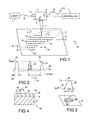
- FIG. 1 shows apparatus for use in the method according to the present invention
- FIG. 2 shows a pulsed laser waveform
- FIG. 3 shows a laser beam that has been focussed onto a surface
- FIG. 4 shows a sample comprising a metal substrate and an anodized surface
- FIGS. 5 and 6 shows a mark being made with different orientations of the mark with the first scanning direction
- FIG. 7 shows the scanning velocity decelerating and accelerating between marks
- FIG. 8 shows a graph of pulse fluence versus absorbed energy density
- FIGS. 9 and 10 show the interlacing of line marking.
- FIG. 1 shows a laser based marking machine 10 comprising a laser 1 , a scanner 2 , and an objective lens 3 .
- the scanner 2 moves a laser beam 4 with respect to an anodized metal surface 5 .
- the scanner 2 comprises a first mirror 6 for moving the laser beam 4 in a first direction 8 , and a second mirror 7 for scanning the laser beam 4 in a second direction 9 .
- the scanner 2 is controlled by a controller 11 which controls the positions of the first and second mirrors 6 , 7 by providing at least one control signal 12 to the scanner 2 .
- the controller 11 may also control the laser 1 .
- the first and the second mirrors 6 , 7 would typically be attached to galvanometers (not shown).
- the laser 1 can be a fibre laser, a solid state rod laser, a solid state disk laser, or a gas laser such as a carbon dioxide laser.
- the laser 1 is preferably a pulsed laser.
- the laser 1 is shown as being connected to the scanner 2 via an optical fibre cable 13 and collimation optics 14 .
- the control signal 12 is depicted as a digital control signal with finite resolution, which would typically be converted into an analogue signal either in the controller 11 or the scanner 2 using a digital to analogue converter. If the digital control signal is incremented slowly, that is, at time increments similar to or larger than the electrical and mechanical time constants in the scanner 2 , then the finite resolution corresponds to finite angular resolution in the positions of the first and second mirrors 6 , 7 , and therefore finite spatial resolution in the position of the laser beam 4 on the surface 5 .
- control signal 12 By filtering the control signal 12 , either electronically, or by means of the inertia of the scanner 2 (for example the inertia of the first and second mirrors 6 , 7 and associated galvanometers), improved angular resolution can typically be achieved in the scanner 2 . This corresponds to improved spatial resolution in the position of the laser beam 4 on the anodized metal surface 5 .
- the series of pulses 21 may be obtained from the laser 1 wherein the laser 1 is a pulsed laser.
- the series of pulses 21 is characterized by a peak power 22 , an average power 23 , a pulse shape 24 , a pulse energy 25 , a pulse width 26 , and a pulse repetition frequency F R 27 .
- FIG. 3 shows a spot 31 formed by focussing the laser beam 4 onto the anodized metal surface 5 .
- the optical intensity 32 is the power per unit area of the laser beam 4 .
- the optical intensity 32 varies across the diameter of the spot 31 from a peak intensity 39 to a 1/e 2 intensity 33 and to zero.
- the diameter of the spot 31 is typically taken as the 1/e 2 diameter 34 , which is the diameter at which the optical intensity 32 falls to the 1/e 2 intensity 33 on either side of the peak intensity 39 .
- the area 35 of the spot 31 is typically taken as the cross-sectional area of the spot 31 within the 1/e 2 diameter 34 .
- FIG. 3 shows the optical intensity 32 varying with a Gaussian or bell-shaped profile.
- the optical intensity 32 may have other profiles, including a top hat profile that is substantially uniform within the beam diameter.
- Pulse fluence 36 is defined as the energy per unit area of the pulse 21 . Pulse fluence is typically measured in J/cm 2 , and is an important parameter for laser marking because a mark is typically formed when the pulse fluence 36 is greater than a pulse fluence threshold 82 of a material shown with reference to FIG. 8 .
- the method comprises:
- spot to spot separation 18 it is meant the distance from the centres of adjacent spots 31 as each line 15 is written once.
- the separation 18 may be uniform, or may vary.
- the separation 18 may be the same in different directions.
- the separation 18 may be different in different directions.
- the pulse fluence is typically in the range 0.02 J/cm 2 to 10 J/cm 2 .
- the pulse fluence is in the range 0.3 J/cm 2 to 5 J/cm 2 .
- the pulse fluence is in the range 0.5 J/cm 2 to 2 J/cm 2 .
- the pulse width is typically in the range 00 ps to 25 ns.
- the pulse width is in the range 300 ps to 10 ns. More preferably the pulsed width is in the range 500 ps to 5 ns.
- pulse width it is meant the full width half maximum duration of the pulse.
- the peak power is preferably greater than 1 kW.
- peak power it is meant the maximum power level during the duration of the pulse.
- the scanning speed is typically in the range 2 to 25 m/s. Preferably the scanning speed is in the range 5 to 15 m/s. More preferably the scanning speed is the range 7 to 10 m/s.
- each line 15 is written by scanning the first mirror 6 while holding the second mirror 7 stationary.
- the hatch distance 19 is achieved by moving the second mirror 7 . This is advantageous because it reduces delays in setting up the control parameters in the controller 11 .
- the second mirror 7 may be characterized by a digital resolution 101 shown with reference to FIG. 1 .
- the hatch distance 19 corresponds to an integral multiple of the digital resolution 101 .
- a typical scanner may have a digital resolution 101 corresponding to a hatch distance 19 of 2 ⁇ m (typically the product of the angular digital resolution measured in radians and the focal length of the lens 3 ).
- a hatch distance 19 of 2 ⁇ m typically the product of the angular digital resolution measured in radians and the focal length of the lens 3 .
- the method of the present invention as described above with reference to FIGS. 1-3 is particularly attractive because it is able to produce marks on anodized metal surfaces faster, and therefore, more economically than has hitherto been possible.
- a black mark could be obtained with lines that are written only once, with spot to spot separations of approximately 10 ⁇ m and a hatch distance 19 of approximately 0.2 ⁇ m.
- considerable time will be spent between scans when using a typical scanner with a digital resolution 12 corresponding to 2 ⁇ m as a relatively complicated waveform needs to be derived to control the scanner to achieve a sub-digital resolution 12 of 0.2 ⁇ m.
- the method of the present invention is able to achieve significant increases in processing speeds by stepping the scanner by 2 ⁇ m (its digital resolution), and overwriting the lines ten times (equal to the quotient of 2 ⁇ m and 0.2 ⁇ m). Also surprisingly, the method of the present invention is able to provide better uniformity as seen by the naked eye of the mark by overwriting each line than by writing each line only once with a smaller hatch distance 19 .
- the sample 40 comprises a metal 41 and an anodization 42 .
- the metal 41 may be a precipitation hardened aluminium alloy. Precipitation hardened aluminium alloys can be procured from Aalco Metals Ltd of Cobham, Surrey, United Kingdom.
- the metal 41 may have been glass bead blasted. Glass bead blasting can be procured from Sandwell UK Ltd of Towcester, United Kingdom.
- the metal 41 may have been hard anodized to produce the anodization 42 .
- the hard anodization may have a thickness of between 5 um and 25 um. More preferably the thickness is between 10 um and 15 um.
- Hard anodization processing can be procured from Hard Anodising Ltd of Kidderminster, United Kingdom.
- the anodization 42 may be clear. By “clear” it is meant “transparent”.
- the clear anodization may be colorless or may be colored.
- the anodization 42 may be translucent or opaque, and in each case, either colorless or colored. The color can be provided by a dye that is incorporated into the anodization 42 .
- the color of the mark 16 may be grey or black.
- the color may have an L value less than or equal to 40.
- Preferably the L value is no greater than 30.
- a mark having an L value less than or equal to 30 is generally considered to be a black mark.
- a black mark having near perfect finishes that can be written rapidly onto consumer goods is commercially very important. Indeed the speed of writing and the quality of the mark 16 can make the difference between the mark 16 , and the apparatus 10 for making the mark 16 , being commercially viable or non-viable.
- the laser 1 may be a pulsed laser having a pulse width greater than one hundred picoseconds.
- the pulse width may be greater than 1 nanosecond. It is surprising and highly commercially significant that high quality black marks can be made rapidly, and with nanosecond pulsed lasers as opposed to picosecond pulsed lasers that have pulse widths less than approximately 10 ps to 50 ps. This is because nanosecond pulsed lasers are by their very nature lower cost than picosecond lasers, and are much lower cost than femtosecond and picosecond pulsed lasers that have pulse widths less than approximately 50 ps and are which marketed for cold laser processing applications such as cold ablation. Such lasers rely on pulse compression techniques or incorporate pulse compressors. It is preferred that the laser 1 does not include a pulse compressor.
- the laser 1 may be an optical fibre laser having a single mode or a multi mode rare-earth doped fibre.
- the beam quality may correspond to an M 2 less than 2, or preferably less than 1.3.
- the scanner 2 may be accelerated prior to pulsing the laser 1 as shown with reference to FIG. 7 . This step reduces edge effects on the mark 16 by ensuring that the scanner 2 is already moving at its desired speed 17 when the laser 1 is first turned on during each scan.
- the anodized metal surface 5 may be orientated to minimize the overall time taken to form the mark 16 .
- the mark 16 is orientated in direction 51 in FIG. 5 , marked along trajectory 52 that has a total length 53 and a total number 54 of lines 15 .
- the mark 16 is orientated in direction 61 in FIG. 6 , marked along trajectory 62 that has a total length 63 and a total number 64 of lines 15 .
- FIG. 7 shows the velocity 71 of the scanning beam 4 with time 72 as it marks the surface 5 .
- the laser 1 is pulsed while the scanning velocity 71 is approximately constant as shown by the pulses 74 .
- the time 73 is the time taken to decelerate the scan and accelerate the scan in the opposite direction.
- the orientation 61 that minimizes the overall time taken to form the mark 16 can be estimated from the total number 54 , 64 of lines 15 required to make the mark 16 , the scan speed 17 , and the time taken 73 at the end of each line 15 to reverse direction and commence scanning again. This feature is advantageous where it is required to further reduce the overall time taken to produce the mark 16 .
- the overall time taken to produce the mark 16 is related to the overall distance 53 , 63 by the scanning speed 17 and the time 73 required to accelerate and decelerate at the beginning and end of each line 15 .
- the lines 15 can each be scanned a plurality of times.
- the scan speed 17 may be at least 5 m/s. By “at least” it is meant equal to or greater than.
- the pulse repetition frequency 27 may be at least 500 kHz.
- the scan speed 17 may be at least 9 m/s, and the pulse repetition frequency 27 may be at least 900 kHz.
- Such a combination of scan speed 17 and pulse repetition frequency 27 is equivalent to a spot to spot separation 18 of 10 ⁇ m. This is typically around half the 1/e 2 diameter of the focussed laser beam (ie the spot 31 ) that is readily achievable on the anodized metal surface 5 when using a single-mode pulsed fibre laser.
- Each line 15 is preferably overwritten at least 5 times. Although it is possible to scan each line 15 only once with the same pulse repetition frequency 27 , it has been found that thermal damage can occur in the anodized material 5 . Preferably each line 15 is scanned as rapidly as possible in order to minimize thermal damage and thus optimize the quality of the mark.
- the spot to spot separation 18 may be at least half the spot diameter 34 .
- FIG. 8 shows the pulse fluence 36 versus absorbed energy density 83 .
- the mark 16 is formed when the pulse fluence 36 is greater than the pulse fluence threshold 82 .
- the individual pulses heat up the anodized metal surface 5 .
- the absorbed energy density 83 exceeds an absorbed energy density threshold 84
- the anodization 42 (shown with reference to FIG. 4 ) cracks or shatters. Such cracks or shattering is undesirable when forming a mark 16 of high quality. It is therefore preferred that the marking process achieves a pulse fluence 36 greater than the pulse fluence threshold 82 , but that the absorbed energy density 83 is less than the absorbed energy density threshold 84 of the product sample 40 .
- absorbed energy density 83 it is meant the absorbed energy density on the surface 5 that is absorbed and retained in a circular area 44 having a circumference 45 approximately one to five times the thickness 43 of the anodization 42 shown with reference to FIG. 4 .
- the absorbed energy density 83 will increase following every pulse delivered in the region of the circular area 44 , but will decrease with heat flow out of the circular area 44 , either laterally along the surface 5 , or through into the metal 41 .
- repeated writing of the lines 15 is advantageous because it permits time for heat flow out of the circular area 44 between the time each line 15 is written.
- a darker mark 16 that is of higher quality can be produced by writing each line 15 five times than by writing a mark with each line 15 written only once with a scan speed 17 five times more slowly.
- the other parameters are held constant, ie both marks are written with the same peak power 22 , average power 23 , pulse shape 24 , pulse energy 25 , pulse width 26 , pulse repetition frequency 27 and pulse fluence 36 .
- the method of the invention includes the step of writing each line 15 more than once, the writing of different ones of the lines 15 can be interlaced by, for example, following a path 91 shown in FIG. 9 where the direction of the scanning is indicated by the arrows.
- the distance 92 between the lines 15 that are being written is preferably greater than the thickness 43 of the anodization 43 , and more preferably greater than five times the thickness 43 of the anodization 43 .
- the scanning path 91 can be incremented as shown in FIG. 10 to a new scanning path 101 in which the lines 15 can be adjacent to those written previously (as shown in FIG. 10 ), or non-adjacent.
- the advantage of such an approach is that it gives more time for heat energy to dissipate while each line 15 is being written, and thus the absorbed energy density 83 is reduced. This reduces the risk of cracking or shattering of the anodization 43 , or alternatively, permits the scanning speed 17 to be increased.
- This interlacing approach can be modified by writing in multiple zig zags, by varying which line 15 is being written on a random or pseudo random basis, or by other writing patterns that achieve interlacing during the repeated scanning of each line 15 .
- the laser 1 can be pulsed during the time 73 at a pulse fluence 36 that is less than the pulse fluence threshold 82 of the sample 40 .
- the advantage of so doing is to reduce the thermal gradient at the edges of the mark 16 .
- the pulse fluence 36 during the time 73 is at least five times less than the pulse fluence threshold 82 .
- the method described above may be used to mark a wide variety of articles including, for example, mobile phones, tablet computers, televisions, machinery, and jewellery.
- the laser 1 shown with reference to FIG. 1 was a pulsed fibre laser model number SP-020P-A-EP-S-A-Y, manufactured by SPI Lasers UK Ltd of Southampton, England.
- the scanner 2 was a galvanometric scan-head model SuperScan II, manufactured by Raylase GmbH of Wessling Germany.
- the objective lens 3 was a 163 mm focal length f-theta objective lens.
- the laser beam 4 was delivered from the laser 1 to the scanner 2 via a 75 mm beam expanding collimator (BEC) 14 which enabled the laser beam 4 to have a nominal diameter of 8 mm (1/e 2 ) at the entrance to the scanner 2 , and a spot diameter 36 of 34 ⁇ m+/ ⁇ 5.0 ⁇ m to be generated at the focal plane of the scanner objective lens 3 .
- BEC beam expanding collimator
- the anodized metal surface 5 was placed at or near to this focal plane.
- the laser 1 was capable of generating pulses in the nanosecond duration range (between approximately 3 ns to approximately 500 ns) and was operated over a range of average output power, laser pulse frequency and temporal pulse shape (which is referred to as a waveform for this type of laser). In this way the pulse energy 25 and pulse peak power 22 were able to be accurately controlled.
- the scanner 2 was able to scan the laser beam 4 with a scan speed 17 of up to 10 m/s (for the specified focal length of scanner objective lens 3 used in this case). The scan speed 17 was able to be accurately controlled so that when the laser 1 was operating at a known pulse repetition frequency 27 , the number of laser pulses per unit length of movement could be calculated.
- the anodized metal surface 5 was the topside of a sample of precipitation hardened aluminium alloy that had been glass bead blasted and hard anodized.
- the hard anodization had a thickness 43 of approximately 10 ⁇ m.
- the method of the invention is able to produce black marks without the characteristic shattering experienced with prior nanosecond laser marking.
Landscapes
- Physics & Mathematics (AREA)
- Optics & Photonics (AREA)
- Engineering & Computer Science (AREA)
- Plasma & Fusion (AREA)
- Mechanical Engineering (AREA)
- Ceramic Engineering (AREA)
- Chemical & Material Sciences (AREA)
- Chemical Kinetics & Catalysis (AREA)
- General Chemical & Material Sciences (AREA)
- Oil, Petroleum & Natural Gas (AREA)
- Laser Beam Processing (AREA)
- Thermal Transfer Or Thermal Recording In General (AREA)
Abstract
A method for laser marking an anodized metal surface (5) with a desired color, which method comprises: providing a laser (1) for emitting a laser beam (4) comprising laser pulses having a pulse energy, a pulse width, and a pulse repetition frequency; providing a scanner (2) comprising a first mirror (6) for scanning the laser beam in a first direction (8), and a second mirror (7) for scanning the laser beam in a second direction (9); providing a lens (3) for focussing the laser beam from the laser (2) onto the anodized metal surface (5) to form a spot (31) having a spot diameter and a pulse fluence; providing a controller (11) for controlling the scanner (2) with a control signal (12); marking a plurality of lines (15) separated by a hatch distance (19) on the anodized metal surface to form a desired mark (16) by scanning the scanner (2) while pulsing the laser (1); selecting a scan speed (16), the pulse repetition frequency, and the spot diameter such that the separation (18) between consecutive spots (31) during each scan of the scanner (2) is at least one quarter of the spot diameter; the method being characterized by: overwriting each line (15) more than once; the color being given by the spot to spot separation (18), hatch distance (19), the pulse fluence, the pulse width, and the number of times each line is written; and selecting the spot to spot separation (18), the hatch distance (19), the pulse fluence, the pulse width, and the number of times each line is written to form the desired color.
Description
This invention relates to a method for laser marking an anodized metal surface with a desired color. The invention has particular application for rapidly marking anodized aluminium consumer goods with high quality black marks without the use of dyes, inks or other chemicals.
The use of dyes, inks and other chemicals in the marking of commercial, consumer and industrial goods places restrictions on supply chains, logistics and the environment. Processes that can mark without the use of dyes, inks or other chemicals can therefore provide a distinct advantage. Laser marking is also generally more versatile, reproducible, and can provide marks that have a higher quality and durability than chemical methods such as silk screens.
Laser marking has been applied to many materials including metals. Once perfected for a particular material, the laser marking process is typically reliable, repeatable, and amenable to high-throughput high-yield production. An example is the color marking of anodized aluminium, a material that is in widespread use as it is lightweight, strong, easily shaped, and has a durable surface finish. The anodized surface is generally dyed with colored dyes. However it is also possible to laser mark anodized aluminium without the use of dyes, inks or other chemicals. Laser light can be used directly to form various colors either within the anodization or in the interface region between the oxide layer that forms the anodization and the aluminium. Similar marks can also be made on other anodized metal surfaces such as titanium, zinc, magnesium, niobium and tantalum.
It is very desirable in consumer goods to have a mark that is distinctive in shape, quality and color, and have a high color contrast to the surrounding material. High quality black marks in anodized aluminium are highly desirable and commercially very important.
U.S. Pat. No. 6,777,098 describes a method of marking anodized aluminium articles with black marks which occur in a layer between the anodization and the aluminium and therefore are as durable as the anodized surface. The marks described therein are described as being dark grey or black in hue and somewhat less shiny than unmarked portion using nanosecond range infrared laser pulses. As taught in U.S. Pat. No. 8,451,873, making marks according to the methods claimed in U.S. Pat. No. 6,777,098 are disadvantageous because (i) creating commercially desirable black marks with nanosecond range pulses tends to cause destruction of the oxide layer, and (ii) cleaning of the aluminium following polishing or other processing adds another step in the process, with associated expense, and possibly disturbs a desired surface finish.
U.S. Pat. No. 8,451,873 discloses a method for creating a mark on an anodized specimen. The method involves providing a laser marking system having controllable laser pulse parameters, determining the laser pulse parameters associated with the desired properties, and directing the laser marking system to mark the article using the selected laser pulse parameters. Laser marks so made have an optical density that ranges from transparent to opaque, a white color, a texture indistinguishable from the surrounding article, and durable, substantially intact anodization. The patent teaches that marks created using laser pulses greater than 1 nanosecond results in clear signs of cracking of the anodization. In particular, the patent teaches that when marking with prior art nanosecond pulses, applying enough laser pulse energy to the surface to make dark marks causes damage to the anodization which causes the appearance of the marks to change with viewing angle. The patent also teaches solving this problem by using pulses having pulse widths of approximately 10 ps. Marks produced by using pulses having pulse widths of approximately 10 ps or less do not damage the anodization, regardless of how dark the marks are, and nor do the marks change in appearance with viewing angle. Such marks are typical of so-called “cold processing” that utilize multi-photon absorption effects in the material. Cold processing (such as cold ablation) does not rely on thermal effects to produce the desired processing effect, and therefore has little if any thermal damage surrounding the processed area. Cold processing relies on femtosecond lasers, or picosecond lasers having pulse widths up to around 10 ps to 50 ps. The marks, quantified by the CIE system of colorimetry, have a chromaticity less than L=40, a=5, and b=10. Although the picosecond lasers used in the patent were much less expensive than femtosecond lasers, the picosecond lasers users are more expensive than nanosecond lasers because they rely on very advanced techniques and components such as optical pulse compressors to produce the very narrow laser pulse widths. Moreover, an L value lower than approximately 30 is more commercially important, and for this, the picosecond lasers used do not write the marks quickly enough for many commercial applications where cost is at a premium. It is advantageous not to rely on expensive techniques or components such as optical pulse compression and optical pulse compressors.
The damage to the anodization layers caused by the use of nanosecond lasers is a particular problem. It is believed that this is caused by thermal effects, and heat build up below the anodization layer as consecutive pulses are written.
There is a need for a method for laser marking a metal surface with a desired color that avoids the aforementioned problems.
Accordingly, in one non-limiting embodiment of the present invention there is provided a method for laser marking an anodized metal surface with a desired color, which method comprises: providing a laser for emitting a laser beam comprising laser pulses having a pulse energy, a pulse width, and a pulse repetition frequency; providing a scanner comprising a first mirror for scanning the laser beam in a first direction, and a second mirror for scanning the laser beam in a second direction; providing a lens for focussing the laser beam from the laser onto the anodized metal surface to form a spot having a spot diameter and a pulse fluence; providing a controller for controlling the scanner with a control signal; marking a plurality of lines separated by a hatch distance on the anodized metal surface to form a desired mark by scanning the scanner while pulsing the laser; and selecting a scan speed, the pulse repetition frequency, and the spot diameter such that the separation between consecutive spots during each scan of the scanner is at least one quarter of the spot diameter; the method being characterized by overwriting each line more than once, the color being given by the spot to spot separation, the hatch distance, the pulse fluence, the pulse width, and the number of times each line is written; and selecting the spot to spot separation, the hatch distance, the pulse fluence, the pulse width, and the number of times each line is written to form the desired color.
The method of the present invention is particularly attractive because it is able to produce marks on anodized metal surfaces faster, and therefore more economically, than has hitherto been possible. For example, a black mark can be obtained with lines that are written only once, with spot to spot separations of approximately 10 μm and line to line spacings (hatching) of approximately 0.2 μm. Considerable time will be spent between scans when using a typical scanner with a “digital” resolution of 2 μm as a relatively complicated waveform needs to be derived to control the scanner to achieve a sub-digital resolution of 0.2 μm. Surprisingly, however, with the method of the present invention, significant increases in processing speeds can be achieved by stepping the scanner by approximately 2 μm (its digital resolution), and overwriting the lines ten times (equal to the quotient of 2 μm and 0.2 μm). Not only is the processing speed increased, marks made on anodized aluminium are darker. This is surprising because it would not have been expected that darker marks could be made more quickly by overwriting lines than by making the same number of passes with each pass incremented with respect to the previous pass.
Each line may be written by scanning the first mirror while holding the second mirror stationary. Other ways of writing the lines may be employed, for example the angular position of the second mirror can be incremented in proportion to the angular position of the first mirror. However this is not preferred.
The hatch distance may be achieved by moving the second mirror.
The second mirror may be characterized by a digital resolution, and the hatch distance may correspond to an integral multiple of the digital resolution.
The metal may be a precipitation hardened aluminium alloy. Other metals may be employed, for example anodized titanium, zinc, magnesium, niobium and tantalum.
The metal may have been glass bead blasted.
The metal may have been hard anodized.
The anodization may have a thickness between 5 μm and 25 μm. The thickness may be between 5 μm and 15 μm.
The anodization may be clear. Alternatively or additionally, the anodization may be colored.
The color may be any suitable color, for example black or gray. When the color is black, then a black mark that can be written rapidly onto consumer goods having near perfect finishes. This is commercially very important and indeed it can make the difference between the mark being commercially viable or non-viable.
The color may be gray or black with an L value no greater than 40. Preferably the L value is no greater than 30. A mark with an L value no greater than 30 would generally be considered to be a black mark.
The laser may be a pulsed laser providing a laser beam having a pulse width greater than one hundred picoseconds. The pulse width may be greater than 1 nanosecond. It is highly significant that high quality black marks (L<=30) can be made rapidly, and with nanosecond pulsed lasers as opposed to picosecond pulsed lasers. This is because nanosecond pulsed lasers are by their very nature lower cost than picosecond lasers, and are much lower cost than femtosecond and picosecond pulsed lasers that have pulse widths less than approximately 50 ps and are which marketed for cold laser processing applications such as cold ablation.
The scanner may be accelerated prior to pulsing the laser. This step reduces edge effects by ensuring that the scanner is already moving at its desired speed when the laser is first turned on during each scan.
The anodized metal surface may be orientated to minimize the overall time taken to form the mark. This feature may be employed where it is desired to further reduce the time taken to produce the mark. The time taken is related to the overall distance by the scanning speed, and the time to decelerate the scanner at the end of the line, and accelerate the scanner at the beginning of the line.
The scanning speed may be at least 5 m/s.
The pulse repetition frequency may be at least 500 kHz.
The scanning speed may be at least 9 m/s, and the pulse repetition frequency may be at least 900 kHz. This combination of scanning speed and pulse repetition frequency is equivalent to a spot to spot separation of 10 μm. This is typically around half the 1/e2 diameter of the focussed laser beam (ie the spot) on the surface of the anodized metal.
Each line may be overwritten a plurality of times. Preferably, each line is written at least 5 times, but more or less times may be employed. Although it is possible to scan each line only once with the same pulse repetition frequency, it has been found that thermal damage can occur in the anodized material. It is therefore preferred to write each line as rapidly as possible in order to minimize thermal damage and thus optimize the quality of the mark.
The spot to spot separation may be at least half the spot diameter.
The present invention also provides an article when marked according to the method of the invention. Examples of articles are mobile phones, tablet computers, televisions, machinery, and jewellery.
Embodiments of the invention will now be described solely by way of example and with reference to the accompanying drawings in which:
The laser 1 can be a fibre laser, a solid state rod laser, a solid state disk laser, or a gas laser such as a carbon dioxide laser. For marking anodized metal surfaces, the laser 1 is preferably a pulsed laser. The laser 1 is shown as being connected to the scanner 2 via an optical fibre cable 13 and collimation optics 14.
The control signal 12 is depicted as a digital control signal with finite resolution, which would typically be converted into an analogue signal either in the controller 11 or the scanner 2 using a digital to analogue converter. If the digital control signal is incremented slowly, that is, at time increments similar to or larger than the electrical and mechanical time constants in the scanner 2, then the finite resolution corresponds to finite angular resolution in the positions of the first and second mirrors 6, 7, and therefore finite spatial resolution in the position of the laser beam 4 on the surface 5. By filtering the control signal 12, either electronically, or by means of the inertia of the scanner 2 (for example the inertia of the first and second mirrors 6, 7 and associated galvanometers), improved angular resolution can typically be achieved in the scanner 2. This corresponds to improved spatial resolution in the position of the laser beam 4 on the anodized metal surface 5.
Referring now to FIG. 2 , there is shown a series of pulses 21. The series of pulses 21 may be obtained from the laser 1 wherein the laser 1 is a pulsed laser. The series of pulses 21 is characterized by a peak power 22, an average power 23, a pulse shape 24, a pulse energy 25, a pulse width 26, and a pulse repetition frequency FR 27.
A method according to the invention and for laser marking the anodized metal surface 5 with a desired color will now be described solely by way of example and with reference to FIG. 1 . The method comprises:
-
- providing the
laser 1 for emitting thelaser beam 4 comprising thelaser pulses 21 having thepulse energy 25, thepulse width 26, and the pulse repetition frequency 27 shown with reference toFIG. 2 ; - providing the
scanner 2, which comprises thefirst mirror 6 for scanning thelaser beam 4 in thefirst direction 8, and thesecond mirror 7 for scanning thelaser beam 4 in the second direction 9; - providing the
lens 3 for focussing thelaser beam 4 from thelaser 4 onto the anodizedmetal surface 5 to form thespot 31 having thespot diameter 34 and thepulse fluence 36 shown with reference toFIG. 3 ; - providing the
controller 11 for controlling thescanner 2 with thecontrol signal 12; - marking a plurality of
lines 15 separated by ahatch distance 19 on the anodizedmetal surface 5 to form a desired mark 16 (shown in outline) by scanning thescanner 2 with ascan speed 17 while pulsing thelaser 1; and - selecting the
scan speed 17, the pulse repetition frequency 27, and thespot diameter 34 such that theseparation 18 betweenconsecutive spots 31 during each scan of thescanner 2 is at least one quarter of thespot diameter 34.
- providing the
The method is characterized by:
-
- overwriting each
line 15 more than once; - the color of the
mark 16 being given by the spot to spotseparation 18, thehatch distance 19, thepulse fluence 36, thepulse width 26, and the number of times eachline 15 is written; and - selecting the spot to spot
separation 18, thehatch distance 19, thepulse fluence 36, thepulse width 26, and the number of times eachline 15 is written, to form the desired color.
- overwriting each
By “spot to spot separation” 18, it is meant the distance from the centres of adjacent spots 31 as each line 15 is written once. The separation 18 may be uniform, or may vary. The separation 18 may be the same in different directions. The separation 18 may be different in different directions.
The pulse fluence is typically in the range 0.02 J/cm2 to 10 J/cm2. Preferably the pulse fluence is in the range 0.3 J/cm2 to 5 J/cm2. More preferably the pulse fluence is in the range 0.5 J/cm2 to 2 J/cm2.
The pulse width is typically in the range 00 ps to 25 ns. Preferably the pulse width is in the range 300 ps to 10 ns. More preferably the pulsed width is in the range 500 ps to 5 ns. By pulse width, it is meant the full width half maximum duration of the pulse.
The peak power is preferably greater than 1 kW. By peak power, it is meant the maximum power level during the duration of the pulse.
The scanning speed is typically in the range 2 to 25 m/s. Preferably the scanning speed is in the range 5 to 15 m/s. More preferably the scanning speed is the range 7 to 10 m/s.
Preferably, each line 15 is written by scanning the first mirror 6 while holding the second mirror 7 stationary. Also preferably, the hatch distance 19 is achieved by moving the second mirror 7. This is advantageous because it reduces delays in setting up the control parameters in the controller 11.
The second mirror 7 may be characterized by a digital resolution 101 shown with reference to FIG. 1 . Preferably the hatch distance 19 corresponds to an integral multiple of the digital resolution 101. For example, a typical scanner may have a digital resolution 101 corresponding to a hatch distance 19 of 2 μm (typically the product of the angular digital resolution measured in radians and the focal length of the lens 3). Instead of writing ten individual lines 15 with a hatch distance 19 of 0.2 μm, it has been discovered that marks of the same or similar quality can be written by writing each line 15 ten times using a hatch distance 19 of 2 μm. Not only is this surprising, but it provides a means of significantly reducing the time taken to mark an object. This is because of the removal of superfluous timing delays as the first scanning mirror 6 scans over the same path. The proportion of time taken for typical controllers to increment the hatch distance 19 between successive lines 15 can be significant, particularly when demanding sub-digital resolution.
The method of the present invention as described above with reference to FIGS. 1-3 is particularly attractive because it is able to produce marks on anodized metal surfaces faster, and therefore, more economically than has hitherto been possible. For example, a black mark could be obtained with lines that are written only once, with spot to spot separations of approximately 10 μm and a hatch distance 19 of approximately 0.2 μm. However, considerable time will be spent between scans when using a typical scanner with a digital resolution 12 corresponding to 2 μm as a relatively complicated waveform needs to be derived to control the scanner to achieve a sub-digital resolution 12 of 0.2 μm. Surprisingly, however, the method of the present invention is able to achieve significant increases in processing speeds by stepping the scanner by 2 μm (its digital resolution), and overwriting the lines ten times (equal to the quotient of 2 μm and 0.2 μm). Also surprisingly, the method of the present invention is able to provide better uniformity as seen by the naked eye of the mark by overwriting each line than by writing each line only once with a smaller hatch distance 19.
Referring now to FIG. 4 , there is shown a cross section of a product sample 40 containing the anodized metal surface 5. The sample 40 comprises a metal 41 and an anodization 42. The metal 41 may be a precipitation hardened aluminium alloy. Precipitation hardened aluminium alloys can be procured from Aalco Metals Ltd of Cobham, Surrey, United Kingdom. The metal 41 may have been glass bead blasted. Glass bead blasting can be procured from Sandwell UK Ltd of Towcester, United Kingdom. The metal 41 may have been hard anodized to produce the anodization 42. The hard anodization may have a thickness of between 5 um and 25 um. More preferably the thickness is between 10 um and 15 um. Hard anodization processing can be procured from Hard Anodising Ltd of Kidderminster, United Kingdom. The anodization 42 may be clear. By “clear” it is meant “transparent”. The clear anodization may be colorless or may be colored. Alternatively, the anodization 42 may be translucent or opaque, and in each case, either colorless or colored. The color can be provided by a dye that is incorporated into the anodization 42.
The color of the mark 16 may be grey or black. The color may have an L value less than or equal to 40. Preferably the L value is no greater than 30. A mark having an L value less than or equal to 30 is generally considered to be a black mark. A black mark having near perfect finishes that can be written rapidly onto consumer goods is commercially very important. Indeed the speed of writing and the quality of the mark 16 can make the difference between the mark 16, and the apparatus 10 for making the mark 16, being commercially viable or non-viable.
The laser 1 may be a pulsed laser having a pulse width greater than one hundred picoseconds. The pulse width may be greater than 1 nanosecond. It is surprising and highly commercially significant that high quality black marks can be made rapidly, and with nanosecond pulsed lasers as opposed to picosecond pulsed lasers that have pulse widths less than approximately 10 ps to 50 ps. This is because nanosecond pulsed lasers are by their very nature lower cost than picosecond lasers, and are much lower cost than femtosecond and picosecond pulsed lasers that have pulse widths less than approximately 50 ps and are which marketed for cold laser processing applications such as cold ablation. Such lasers rely on pulse compression techniques or incorporate pulse compressors. It is preferred that the laser 1 does not include a pulse compressor.
The laser 1 may be an optical fibre laser having a single mode or a multi mode rare-earth doped fibre. The beam quality may correspond to an M2 less than 2, or preferably less than 1.3.
The scanner 2 may be accelerated prior to pulsing the laser 1 as shown with reference to FIG. 7 . This step reduces edge effects on the mark 16 by ensuring that the scanner 2 is already moving at its desired speed 17 when the laser 1 is first turned on during each scan.
As shown with reference to FIGS. 5 to 7 , the anodized metal surface 5 may be orientated to minimize the overall time taken to form the mark 16. The mark 16 is orientated in direction 51 in FIG. 5 , marked along trajectory 52 that has a total length 53 and a total number 54 of lines 15. The mark 16 is orientated in direction 61 in FIG. 6 , marked along trajectory 62 that has a total length 63 and a total number 64 of lines 15. FIG. 7 shows the velocity 71 of the scanning beam 4 with time 72 as it marks the surface 5. The laser 1 is pulsed while the scanning velocity 71 is approximately constant as shown by the pulses 74. The time 73 is the time taken to decelerate the scan and accelerate the scan in the opposite direction. It is clear from examining FIGS. 5 and 6 that the total number 54 of lines 15 achieved with orientation 53 is much larger than the total number 64 of lines 15 in FIG. 6 with the orientiation 61. The orientation 61 that minimizes the overall time taken to form the mark 16 can be estimated from the total number 54, 64 of lines 15 required to make the mark 16, the scan speed 17, and the time taken 73 at the end of each line 15 to reverse direction and commence scanning again. This feature is advantageous where it is required to further reduce the overall time taken to produce the mark 16. The overall time taken to produce the mark 16 is related to the overall distance 53, 63 by the scanning speed 17 and the time 73 required to accelerate and decelerate at the beginning and end of each line 15. The lines 15 can each be scanned a plurality of times.
The scan speed 17 may be at least 5 m/s. By “at least” it is meant equal to or greater than.
The pulse repetition frequency 27 may be at least 500 kHz.
The scan speed 17 may be at least 9 m/s, and the pulse repetition frequency 27 may be at least 900 kHz. Such a combination of scan speed 17 and pulse repetition frequency 27 is equivalent to a spot to spot separation 18 of 10 μm. This is typically around half the 1/e2 diameter of the focussed laser beam (ie the spot 31) that is readily achievable on the anodized metal surface 5 when using a single-mode pulsed fibre laser.
Each line 15 is preferably overwritten at least 5 times. Although it is possible to scan each line 15 only once with the same pulse repetition frequency 27, it has been found that thermal damage can occur in the anodized material 5. Preferably each line 15 is scanned as rapidly as possible in order to minimize thermal damage and thus optimize the quality of the mark.
The spot to spot separation 18 may be at least half the spot diameter 34. FIG. 8 shows the pulse fluence 36 versus absorbed energy density 83. As described with reference to FIG. 3 , the mark 16 is formed when the pulse fluence 36 is greater than the pulse fluence threshold 82. However when forming the mark 16, the individual pulses heat up the anodized metal surface 5. When the absorbed energy density 83 exceeds an absorbed energy density threshold 84, the anodization 42 (shown with reference to FIG. 4 ) cracks or shatters. Such cracks or shattering is undesirable when forming a mark 16 of high quality. It is therefore preferred that the marking process achieves a pulse fluence 36 greater than the pulse fluence threshold 82, but that the absorbed energy density 83 is less than the absorbed energy density threshold 84 of the product sample 40.
By absorbed energy density 83, it is meant the absorbed energy density on the surface 5 that is absorbed and retained in a circular area 44 having a circumference 45 approximately one to five times the thickness 43 of the anodization 42 shown with reference to FIG. 4 . The absorbed energy density 83 will increase following every pulse delivered in the region of the circular area 44, but will decrease with heat flow out of the circular area 44, either laterally along the surface 5, or through into the metal 41.
Without wishing to limit the scope of the invention, it is believed that repeated writing of the lines 15 is advantageous because it permits time for heat flow out of the circular area 44 between the time each line 15 is written. For example, a darker mark 16 that is of higher quality (less cracking or shattering of the anodization 42) can be produced by writing each line 15 five times than by writing a mark with each line 15 written only once with a scan speed 17 five times more slowly. In this comparison, the other parameters are held constant, ie both marks are written with the same peak power 22, average power 23, pulse shape 24, pulse energy 25, pulse width 26, pulse repetition frequency 27 and pulse fluence 36.
Although the method of the invention includes the step of writing each line 15 more than once, the writing of different ones of the lines 15 can be interlaced by, for example, following a path 91 shown in FIG. 9 where the direction of the scanning is indicated by the arrows. The distance 92 between the lines 15 that are being written is preferably greater than the thickness 43 of the anodization 43, and more preferably greater than five times the thickness 43 of the anodization 43. Once the lines 15 are written, the scanning path 91 can be incremented as shown in FIG. 10 to a new scanning path 101 in which the lines 15 can be adjacent to those written previously (as shown in FIG. 10 ), or non-adjacent. The advantage of such an approach is that it gives more time for heat energy to dissipate while each line 15 is being written, and thus the absorbed energy density 83 is reduced. This reduces the risk of cracking or shattering of the anodization 43, or alternatively, permits the scanning speed 17 to be increased. This interlacing approach can be modified by writing in multiple zig zags, by varying which line 15 is being written on a random or pseudo random basis, or by other writing patterns that achieve interlacing during the repeated scanning of each line 15.
Referring again to FIG. 7 , the laser 1 can be pulsed during the time 73 at a pulse fluence 36 that is less than the pulse fluence threshold 82 of the sample 40. The advantage of so doing is to reduce the thermal gradient at the edges of the mark 16. Preferably the pulse fluence 36 during the time 73 is at least five times less than the pulse fluence threshold 82.
The method described above may be used to mark a wide variety of articles including, for example, mobile phones, tablet computers, televisions, machinery, and jewellery.
The method of the invention will now be described with reference to the following non-limiting example, which is given for illustrative purposes only.
The laser 1 shown with reference to FIG. 1 was a pulsed fibre laser model number SP-020P-A-EP-S-A-Y, manufactured by SPI Lasers UK Ltd of Southampton, England. The scanner 2 was a galvanometric scan-head model SuperScan II, manufactured by Raylase GmbH of Wessling Germany. The objective lens 3 was a 163 mm focal length f-theta objective lens. The laser beam 4 was delivered from the laser 1 to the scanner 2 via a 75 mm beam expanding collimator (BEC) 14 which enabled the laser beam 4 to have a nominal diameter of 8 mm (1/e2) at the entrance to the scanner 2, and a spot diameter 36 of 34 μm+/−5.0 μm to be generated at the focal plane of the scanner objective lens 3. During normal operation of the workstation 10, the anodized metal surface 5 was placed at or near to this focal plane.
The laser 1 was capable of generating pulses in the nanosecond duration range (between approximately 3 ns to approximately 500 ns) and was operated over a range of average output power, laser pulse frequency and temporal pulse shape (which is referred to as a waveform for this type of laser). In this way the pulse energy 25 and pulse peak power 22 were able to be accurately controlled. The scanner 2 was able to scan the laser beam 4 with a scan speed 17 of up to 10 m/s (for the specified focal length of scanner objective lens 3 used in this case). The scan speed 17 was able to be accurately controlled so that when the laser 1 was operating at a known pulse repetition frequency 27, the number of laser pulses per unit length of movement could be calculated.
The anodized metal surface 5 was the topside of a sample of precipitation hardened aluminium alloy that had been glass bead blasted and hard anodized. The hard anodization had a thickness 43 of approximately 10 μm.
The method of the invention is able to produce black marks without the characteristic shattering experienced with prior nanosecond laser marking.
Similar experiments have been performed on other anodized metal surfaces. These experiments have demonstrated the quality and blackness of the marks, and the improvement in writing the mark according to the method of the invention.
It is to be appreciated that the embodiments of the invention described above with reference to the accompanying drawings have been given by way of example only and that modifications and additional steps and components may be provided to enhance performance. Individual components shown in the drawings are not limited to use in their drawings and may be used in other drawings and in all aspects of the invention. The present invention extends to the above mentioned features taken singly or in any combination.
Claims (20)
1. A method for laser marking an anodized metal surface with a desired colour, which method comprises:
providing a laser for emitting a laser beam comprising laser pulses having a pulse energy, a pulse width, and a pulse repetition frequency;
providing a seamier comprising a first mirror for scanning the laser beam in a first direction, and a second mirror for scanning the laser beam in a second direction;
providing a lens for focussing the laser beam from the laser onto the anodized metal surface to form a spot having a spot diameter and a pulse fluence;
providing a controller for controlling the scanner with a control signal;
marking a plurality of lines separated by a hatch distance on the anodized metal surface to form a desired mark by scanning the scanner while pulsing the laser; and
selecting a scan speed, the pulse repetition frequency, and the spot diameter such that the separation between consecutive spots during each scan of the scanner is at least one quarter of the spot diameter;
the method being characterized by
overwriting each line more than once;
the colour being given by the spot to spot separation, the hatch distance, the pulse fluence, the pulse width, and the number of times each line is written; and
selecting the spot to spot separation, the hatch distance, the pulse fluence, the pulse width, and the number of times each line is written to form the desired colour.
2. A method according to claim 1 wherein the second mirror is characterised by a digital resolution, and the hatch distance corresponds to an integral multiple of the digital resolution.
3. A method according to claim 1 wherein the metal is a precipitation hardened aluminium alloy.
4. A method according to claim 1 wherein the metal has been glass bead blasted.
5. A method according to claim 1 wherein the metal has been hard anodized.
6. A method according to claim 1 wherein the anodization has a thickness between 5 μm and 25 μm.
7. A method according to claim 6 wherein the anodization has a thickness between 5 μm and 15 μm.
8. A method according to claim 1 wherein the anodization is clear.
9. A method according to claim 1 wherein the anodization is coloured.
10. A method according to claim 1 wherein the colour is gray or black with an L value no greater than 40.
11. A method according to claim 10 wherein the L value is no greater than 30.
12. A method according to claim 1 wherein the laser is a pulsed laser providing a laser beam having a pulse width greater than one hundred picoseconds.
13. A method according to claim 12 wherein the pulse width is greater than 1 nanosecond.
14. A method according to claim 1 wherein the scanner is accelerated prior to pulsing the laser.
15. A method according to claim 1 wherein the anodized metal surface is orientated to minimize the overall time taken to form the mark.
16. A method according to claim 1 wherein the scanning speed is at least 5 m/s.
17. A method according to claim 1 wherein the pulse repetition frequency is at least 500 kHz.
18. A method according to claim 1 wherein the scanning speed is at least 9 m/s, and the pulse repetition frequency is at least 900 kHz.
19. A method according to claim 1 wherein each line is overwritten at least 5 times.
20. A method according to claim 1 wherein the spot to spot separation is at least half the spot diameter.
Applications Claiming Priority (3)
| Application Number | Priority Date | Filing Date | Title |
|---|---|---|---|
| GB1321322.8A GB2520945A (en) | 2013-12-03 | 2013-12-03 | Method for laser marking an anodized metal surface with a desired colour |
| GB1321322.8 | 2013-12-03 | ||
| PCT/GB2014/000497 WO2015082869A1 (en) | 2013-12-03 | 2014-12-01 | Method for laser marking an anodized metal surface with a desired colour |
Publications (2)
| Publication Number | Publication Date |
|---|---|
| US20160256955A1 US20160256955A1 (en) | 2016-09-08 |
| US9533370B2 true US9533370B2 (en) | 2017-01-03 |
Family
ID=49979720
Family Applications (1)
| Application Number | Title | Priority Date | Filing Date |
|---|---|---|---|
| US15/036,967 Active US9533370B2 (en) | 2013-12-03 | 2014-12-01 | Method for laser marking an anodized metal surface with a desired colour |
Country Status (5)
| Country | Link |
|---|---|
| US (1) | US9533370B2 (en) |
| EP (1) | EP3077211B1 (en) |
| CN (1) | CN105848914B (en) |
| GB (1) | GB2520945A (en) |
| WO (1) | WO2015082869A1 (en) |
Families Citing this family (20)
| Publication number | Priority date | Publication date | Assignee | Title |
|---|---|---|---|---|
| US20160243646A1 (en) * | 2015-02-23 | 2016-08-25 | Electro Scientific Industries, Inc. | Laser systems and methods for large area modification |
| GB201609086D0 (en) * | 2016-05-20 | 2016-07-06 | Spi Lasers Uk Ltd | Method for creating a mark with a desired colour on an article |
| CN108262564A (en) * | 2017-01-04 | 2018-07-10 | 大族激光科技产业集团股份有限公司 | A kind of laser mark printing device and method |
| CN110102904B (en) * | 2019-04-03 | 2021-11-19 | 大族激光科技产业集团股份有限公司 | Laser marking method and system for watchcase characters |
| DE102019130898A1 (en) | 2019-08-16 | 2021-02-18 | Infineon Technologies Ag | TWO-STAGE LASER PROCESSING OF AN ENCAPSULATING AGENT OF A SEMICONDUCTOR CHIP HOUSING |
| CN111716013A (en) * | 2020-07-23 | 2020-09-29 | 英诺激光科技股份有限公司 | Medical device laser marking system and method |
| CN113096147B (en) * | 2021-04-08 | 2022-07-29 | 中国人民解放军国防科技大学 | MATLAB-based automatic laser marking shadow generation method |
| JP7842210B2 (en) * | 2021-10-14 | 2026-04-07 | ザ プロクター アンド ギャンブル カンパニー | High-speed laser marking on goods |
| US20230124975A1 (en) * | 2021-10-14 | 2023-04-20 | The Procter & Gamble Company | High speed laser processes for marking on articles |
| CN116021157A (en) * | 2021-10-27 | 2023-04-28 | 苏州热工研究院有限公司 | A kind of laser stripping method |
| JP2025501707A (en) * | 2021-12-16 | 2025-01-23 | ザ プロクター アンド ギャンブル カンパニー | High speed laser processes for marking articles |
| EP4448292A1 (en) * | 2021-12-16 | 2024-10-23 | The Procter & Gamble Company | High speed laser processes for marking on articles |
| CN115476056B (en) * | 2022-10-14 | 2026-02-10 | 北京慧骨医学科技有限公司 | Laser beam spot determination method, device, electronic equipment and storage medium |
| US12416519B2 (en) | 2023-03-29 | 2025-09-16 | The Procter & Gamble Company | Measuring cup having a bitmapped pattern |
| US12449295B2 (en) | 2023-03-29 | 2025-10-21 | The Procter & Gamble Company | Measuring cup having a bitmapped pattern |
| US20240326171A1 (en) * | 2023-03-30 | 2024-10-03 | The Procter & Gamble Company | High speed laser processes for marking on articles |
| US12187063B2 (en) | 2023-03-30 | 2025-01-07 | The Procter & Gamble Company | Sheet materials and articles comprising TiO2 and laser marking |
| US12589608B2 (en) | 2023-03-30 | 2026-03-31 | The Procter & Gamble Company | Laser marked articles with machine readable codes |
| US12589609B2 (en) * | 2023-03-30 | 2026-03-31 | The Procter & Gamble Company | Laser marked articles with machine readable codes |
| WO2026006349A1 (en) * | 2024-06-26 | 2026-01-02 | The Procter & Gamble Company | High speed laser processes for marking articles in motion, and marked articles |
Citations (6)
| Publication number | Priority date | Publication date | Assignee | Title |
|---|---|---|---|---|
| US20060103719A1 (en) * | 2000-12-13 | 2006-05-18 | Orbotech Ltd. | Pulse light pattern writer |
| US20070285492A1 (en) * | 2006-06-07 | 2007-12-13 | Mark Edwin Kirtley Lund | Laser Power Switching for Alignment Purposes in a Laser Printer |
| US20110089067A1 (en) | 2009-10-16 | 2011-04-21 | Scott Matthew S | Sub-Surface Marking of Product Housings |
| US20110193928A1 (en) | 2010-02-11 | 2011-08-11 | Electro Scientific Industries, Inc. | Method and apparatus for reliably laser marking articles |
| US20120200656A1 (en) * | 2009-10-19 | 2012-08-09 | Miyuki Oda | Drawing control method, laser irradiating apparatus, drawing control program, and recording medium having recorded therewith |
| WO2012121732A1 (en) | 2011-03-10 | 2012-09-13 | Electro Scientific Industries, Inc. | Method and apparatus for reliably laser marking articles |
Family Cites Families (9)
| Publication number | Priority date | Publication date | Assignee | Title |
|---|---|---|---|---|
| WO2001034408A1 (en) * | 1999-11-11 | 2001-05-17 | Koninklijke Philips Electronics N.V. | Marking of an anodized layer of an aluminium object |
| JP2008265344A (en) * | 2003-01-28 | 2008-11-06 | Iwakura Yosetsu Kogyosho:Kk | Color marking method using laser |
| CN100379566C (en) * | 2003-04-28 | 2008-04-09 | 富士胶片株式会社 | Device and method for laser marking |
| US7005603B2 (en) * | 2004-04-02 | 2006-02-28 | Hewlett-Packard Development Company, L.P. | Laser marking |
| JP4782626B2 (en) * | 2006-07-07 | 2011-09-28 | 静岡県 | Laser marking method |
| CN101564947B (en) * | 2009-05-25 | 2010-12-08 | 深圳市大族激光科技股份有限公司 | A method of laser marking on plastic |
| US8379679B2 (en) * | 2010-02-11 | 2013-02-19 | Electro Scientific Industries, Inc. | Method and apparatus for reliably laser marking articles |
| PL222531B1 (en) * | 2012-04-05 | 2016-08-31 | Wrocławskie Centrum Badań Eit + Spółka Z Ograniczoną | Method and system for color marking of metals |
| CN203198410U (en) * | 2013-02-25 | 2013-09-18 | 伊欧激光科技(苏州)有限公司 | Laser mark device |
-
2013
- 2013-12-03 GB GB1321322.8A patent/GB2520945A/en not_active Withdrawn
-
2014
- 2014-12-01 EP EP14809945.0A patent/EP3077211B1/en active Active
- 2014-12-01 US US15/036,967 patent/US9533370B2/en active Active
- 2014-12-01 WO PCT/GB2014/000497 patent/WO2015082869A1/en not_active Ceased
- 2014-12-01 CN CN201480066022.6A patent/CN105848914B/en active Active
Patent Citations (6)
| Publication number | Priority date | Publication date | Assignee | Title |
|---|---|---|---|---|
| US20060103719A1 (en) * | 2000-12-13 | 2006-05-18 | Orbotech Ltd. | Pulse light pattern writer |
| US20070285492A1 (en) * | 2006-06-07 | 2007-12-13 | Mark Edwin Kirtley Lund | Laser Power Switching for Alignment Purposes in a Laser Printer |
| US20110089067A1 (en) | 2009-10-16 | 2011-04-21 | Scott Matthew S | Sub-Surface Marking of Product Housings |
| US20120200656A1 (en) * | 2009-10-19 | 2012-08-09 | Miyuki Oda | Drawing control method, laser irradiating apparatus, drawing control program, and recording medium having recorded therewith |
| US20110193928A1 (en) | 2010-02-11 | 2011-08-11 | Electro Scientific Industries, Inc. | Method and apparatus for reliably laser marking articles |
| WO2012121732A1 (en) | 2011-03-10 | 2012-09-13 | Electro Scientific Industries, Inc. | Method and apparatus for reliably laser marking articles |
Also Published As
| Publication number | Publication date |
|---|---|
| US20160256955A1 (en) | 2016-09-08 |
| EP3077211A1 (en) | 2016-10-12 |
| CN105848914B (en) | 2017-12-15 |
| WO2015082869A1 (en) | 2015-06-11 |
| GB2520945A (en) | 2015-06-10 |
| EP3077211B1 (en) | 2018-02-07 |
| GB201321322D0 (en) | 2014-01-15 |
| CN105848914A (en) | 2016-08-10 |
Similar Documents
| Publication | Publication Date | Title |
|---|---|---|
| US9533370B2 (en) | Method for laser marking an anodized metal surface with a desired colour | |
| EP3458274B1 (en) | Method for creating a mark with a desired colour on an article | |
| US9138826B2 (en) | Method for laser marking a metal surface with a desired colour | |
| EP2922657B1 (en) | Method for laser marking a metal surface with a desired colour | |
| US6768081B2 (en) | Method and laser system for production of high quality laser-induced damage images by using material processing made before and after image creation | |
| TWI679077B (en) | Methods for laser drilling materials and glass articles | |
| US20170247289A1 (en) | Coated glass or glass ceramic article | |
| US6670576B2 (en) | Method for producing images containing laser-induced color centers and laser-induced damages | |
| US20140175067A1 (en) | Methods of forming images by laser micromachining | |
| US20160243646A1 (en) | Laser systems and methods for large area modification | |
| JPH11267861A (en) | Marking of optical transmitting material | |
| JP6474810B2 (en) | Laser system and method for marking inside a thin layer and object produced thereby | |
| KR20180013678A (en) | Method and apparatus for laser processing substrate of brittle material | |
| JP2004181496A (en) | Laser beam machining method, transparent resin member product machined by the method, and display device using the transparent resin member product | |
| KR102353478B1 (en) | Method and apparatus for laser processing substrate of brittle material | |
| DE102005055330B4 (en) | Process for the partial removal of textile particles from the surface of a ceramic or metal article | |
| KR100683437B1 (en) | Laser processing method | |
| Patwa et al. | Laser color marking with color monitoring | |
| US20060255020A1 (en) | Method for production of laser-induced images inside liquids |
Legal Events
| Date | Code | Title | Description |
|---|---|---|---|
| STCF | Information on status: patent grant |
Free format text: PATENTED CASE |
|
| MAFP | Maintenance fee payment |
Free format text: PAYMENT OF MAINTENANCE FEE, 4TH YEAR, LARGE ENTITY (ORIGINAL EVENT CODE: M1551); ENTITY STATUS OF PATENT OWNER: LARGE ENTITY Year of fee payment: 4 |
|
| AS | Assignment |
Owner name: TRUMPF LASER UK LIMITED, UNITED KINGDOM Free format text: CHANGE OF NAME;ASSIGNOR:SPI LASERS UK LIMITED;REEL/FRAME:069442/0478 Effective date: 20201120 |