US9529954B1 - Standard cell library with DFM-optimized M0 cuts - Google Patents

Standard cell library with DFM-optimized M0 cuts Download PDF

Info

Publication number
US9529954B1
US9529954B1 US15/067,252 US201615067252A US9529954B1 US 9529954 B1 US9529954 B1 US 9529954B1 US 201615067252 A US201615067252 A US 201615067252A US 9529954 B1 US9529954 B1 US 9529954B1
Authority
US
United States
Prior art keywords
logic function
input
logic
cell
function
Prior art date
Legal status (The legal status is an assumption and is not a legal conclusion. Google has not performed a legal analysis and makes no representation as to the accuracy of the status listed.)
Expired - Fee Related, expires
Application number
US15/067,252
Inventor
Jonathan HAIGH
Current Assignee (The listed assignees may be inaccurate. Google has not performed a legal analysis and makes no representation or warranty as to the accuracy of the list.)
PDF Solutions Inc
Original Assignee
PDF Solutions Inc
Priority date (The priority date is an assumption and is not a legal conclusion. Google has not performed a legal analysis and makes no representation as to the accuracy of the date listed.)
Filing date
Publication date
Application filed by PDF Solutions Inc filed Critical PDF Solutions Inc
Priority to US15/067,252 priority Critical patent/US9529954B1/en
Assigned to PDF SOLUTIONS, INC. reassignment PDF SOLUTIONS, INC. ASSIGNMENT OF ASSIGNORS INTEREST (SEE DOCUMENT FOR DETAILS). Assignors: Haigh, Jonathan
Priority to US15/131,020 priority patent/US9461065B1/en
Priority to US15/134,420 priority patent/US9595536B1/en
Priority to US15/259,333 priority patent/US9627408B1/en
Application granted granted Critical
Publication of US9529954B1 publication Critical patent/US9529954B1/en
Assigned to WELLS FARGO BANK, NATIONAL ASSOCIATION, AS ADMINISTRATIVE AGENT reassignment WELLS FARGO BANK, NATIONAL ASSOCIATION, AS ADMINISTRATIVE AGENT SECURITY INTEREST (SEE DOCUMENT FOR DETAILS). Assignors: PDF SOLUTIONS, INC.
Expired - Fee Related legal-status Critical Current
Adjusted expiration legal-status Critical

Links

Images

Classifications

    • G06F17/5068
    • GPHYSICS
    • G06COMPUTING OR CALCULATING; COUNTING
    • G06FELECTRIC DIGITAL DATA PROCESSING
    • G06F30/00Computer-aided design [CAD]
    • G06F30/30Circuit design
    • G06F30/39Circuit design at the physical level
    • H01L27/0207
    • H01L27/11807
    • HELECTRICITY
    • H10SEMICONDUCTOR DEVICES; ELECTRIC SOLID-STATE DEVICES NOT OTHERWISE PROVIDED FOR
    • H10DINORGANIC ELECTRIC SEMICONDUCTOR DEVICES
    • H10D84/00Integrated devices formed in or on semiconductor substrates that comprise only semiconducting layers, e.g. on Si wafers or on GaAs-on-Si wafers
    • H10D84/90Masterslice integrated circuits
    • H10D84/903Masterslice integrated circuits comprising field effect technology
    • H10D84/907CMOS gate arrays
    • HELECTRICITY
    • H10SEMICONDUCTOR DEVICES; ELECTRIC SOLID-STATE DEVICES NOT OTHERWISE PROVIDED FOR
    • H10DINORGANIC ELECTRIC SEMICONDUCTOR DEVICES
    • H10D89/00Aspects of integrated devices not covered by groups H10D84/00 - H10D88/00
    • H10D89/10Integrated device layouts
    • H01L2027/11883
    • HELECTRICITY
    • H10SEMICONDUCTOR DEVICES; ELECTRIC SOLID-STATE DEVICES NOT OTHERWISE PROVIDED FOR
    • H10DINORGANIC ELECTRIC SEMICONDUCTOR DEVICES
    • H10D84/00Integrated devices formed in or on semiconductor substrates that comprise only semiconducting layers, e.g. on Si wafers or on GaAs-on-Si wafers
    • H10D84/90Masterslice integrated circuits
    • H10D84/903Masterslice integrated circuits comprising field effect technology
    • H10D84/907CMOS gate arrays
    • H10D84/983Levels of metallisation
    • H10D84/985Two levels of metal

Definitions

  • This invention relates to design for manufacturability (DFM) of standard cells for advanced semiconductor processes (e.g., 10 nm, 7 nm), to libraries containing such cells, and to wafers/chips that contain instances of such cells.
  • DFM manufacturability
  • One aspect relates to a library of DFM-improved standard cells, optimized for use in advanced semiconductor processes that include multi-patterned M0 cut masks.
  • Another aspect of the invention relates to wafers, chips, and systems that include such DFM-improved cells.
  • the present invention provides a library of competitively dense logic cells with highly-optimized patterning in the first-level metal (M0) layer. As described in greater detail below, such patterning avoids spacing M0 cuts so close that they increase the risk of manufacturing failure.
  • each standard cell comprises, for example, at least the following: two elongated supply rails, each formed in a first metal (M0) layer, each supply rail having a width at least twice a minimum permitted width for M0 features, and each supply rail extending horizontally across the entire width of the standard cell; at least three elongated gate stripes, each formed in a gate (PC) layer, and each extending vertically between at least two of the supply rails, with adjacent gate stripes spaced at a minimum contacted poly pitch (CPP); positioned vertically between the supply rails, at least two, first-exposure M0 tracks, each of the first-exposure M0 tracks having the minimum permitted width and extending horizontally across the cell, the first-exposure M0 tracks patterned, in part, by portion(s) of a first-exposure M0 mask (M0_color1) and, in part, by portion
  • Such collections may be embodied on silicon wafers, chips, or systems, or as instructions for patterning such cells, where such instruction are contained in a non-transient, computer-readable mediums, in data formats such as GDSII.
  • Such collections preferably include cells implementing at least four, six, eight, ten, twelve, fourteen, sixteen, eighteen, twenty or more logical functions selected from the following list, each of which may be provided in multiple drive strength variants:
  • each standard cell comprises, for example, at least the following: at least two elongated supply rails, extending horizontally across the standard cell; at least three elongated gate stripes, each extending vertically between at least two of said supply rails, adjacent gate stripes spaced at a minimum contacted poly pitch (CPP); positioned vertically between the supply rails, one or more first-exposure M0 tracks, each of the first-exposure M0 tracks having a minimum permitted width for M0 patterning and extending horizontally across the cell, the first-exposure M0 tracks patterned, in part, by feature(s) of a first-exposure M0 mask (M0_color1) and, in part, by feature(s) of a first-exposure M0 cut mask (M0CUT1); positioned vertically between the supply rails, one or more second-exposure M0 tracks, each of the second-exposure
  • FIGS. 1A-C depict an sdffqx1_alt cell
  • FIGS. 2A-C depict a mux2x1_alt cell
  • FIGS. 3A-C depict an an2x1 cell
  • FIGS. 4A-C depict an an2x2 cell
  • FIGS. 5A-C depict an an3x1 cell
  • FIGS. 6A-C depict an an3x2 cell
  • FIGS. 7A-C depict an an4x1 cell
  • FIGS. 8A-C depict an an4x2 cell
  • FIGS. 9A-C depict an ao21x1 cell
  • FIGS. 10A-C depict an ao31x1 cell
  • FIGS. 11A-C depict an ao211x1 cell
  • FIGS. 12A-C depict an aoi21x1 cell
  • FIGS. 13A-C depict an aoi21x2 cell
  • FIGS. 14A-C depict an aoi22x1 cell
  • FIGS. 15A-C depict an aoi22x2 cell
  • FIGS. 16A-C depict an aoi31x1 cell
  • FIGS. 17A-C depict an aoi31x2 cell
  • FIGS. 18A-C depict an aoi211x1 cell
  • FIGS. 19A-C depict an aoi222x1 cell
  • FIGS. 20A-C depict an bufhx6 cell
  • FIGS. 21A-C depict an bufx1 cell
  • FIGS. 22A-C depict an bufx2 cell
  • FIGS. 23A-C depict an bufx3 cell
  • FIGS. 24A-C depict an bufx4 cell
  • FIGS. 25A-C depict an bufx6 cell
  • FIGS. 26A-C depict an bufx8 cell
  • FIGS. 27A-C depict an ckor21ban2x1 cell
  • FIGS. 28A-C depict an dlyx1 cell
  • FIGS. 29A-C depict an fax1 cell
  • FIGS. 30A-C depict an hax1 cell
  • FIGS. 31A-C depict an iaoi21x1 cell
  • FIGS. 32A-C depict an ind2x1 cell
  • FIGS. 33A-C depict an ind2x2 cell
  • FIGS. 34A-C depict an ind3x1 cell
  • FIGS. 35A-C depict an ind3x2 cell
  • FIGS. 36A-C depict an inr2x1 cell
  • FIGS. 37A-C depict an inr2x2 cell
  • FIGS. 38A-C depict an inr3x1 cell
  • FIGS. 39A-C depict an inr3x2 cell
  • FIGS. 40A-C depict an invx1 cell
  • FIGS. 41A-C depict an invx2 cell
  • FIGS. 42A-C depict an invx4 cell
  • FIGS. 43A-C depict an invx6 cell
  • FIGS. 44A-C depict an invx8 cell
  • FIGS. 45A-C depict an ioai21x1 cell
  • FIGS. 46A-C depict an latqx1 cell
  • FIGS. 47A-C depict an mux2x1 cell
  • FIGS. 48A-C depict an mux2x2 cell
  • FIGS. 49A-C depict an muxi2x1 cell
  • FIGS. 50A-C depict an nd2x1 cell
  • FIGS. 51A-C depict an nd2x2 cell
  • FIGS. 52A-C depict an nd2x3 cell
  • FIGS. 53A-C depict an nd2x4 cell
  • FIGS. 54A-C depict an nd3x1 cell
  • FIGS. 55A-C depict an nd3x2 cell
  • FIGS. 56A-C depict an nd3x3 cell
  • FIGS. 57A-C depict an nd3x4 cell
  • FIGS. 58A-C depict an nd4x1 cell
  • FIGS. 59A-C depict an nd4x2 cell
  • FIGS. 60A-C depict an nr2x1 cell
  • FIGS. 61A-C depict an nr2x2 cell
  • FIGS. 61.1A-C depict an nr2x3 cell
  • FIGS. 62A-C depict an nr2x4 cell
  • FIGS. 63A-C depict an nr3x1 cell
  • FIGS. 64A-C depict an nr3x2 cell
  • FIGS. 65A-C depict an nr3x3 cell
  • FIGS. 66A-C depict an nr3x4 cell
  • FIGS. 67A-C depict an nr4x1 cell
  • FIGS. 68A-C depict an nr4x2 cell
  • FIGS. 69A-C depict an oa21x1 cell
  • FIGS. 70A-C depict an oa31x1 cell
  • FIGS. 71A-C depict an oa211x1 cell
  • FIGS. 72A-C depict an oai21x1 cell
  • FIGS. 73A-C depict an oai21x2 cell
  • FIGS. 74A-C depict an oai22x1 cell
  • FIGS. 75A-C depict an oai22x2 cell
  • FIGS. 76A-C depict an oai31x1 cell
  • FIGS. 77A-C depict an oai31x2 cell
  • FIGS. 78A-C depict an oai211x1 cell
  • FIGS. 79A-C depict an oai222x1 cell
  • FIGS. 80A-C depict an or2x1 cell
  • FIGS. 81A-C depict an or2x2 cell
  • FIGS. 82A-C depict an or3x1 cell
  • FIGS. 83A-C depict an or3x2 cell
  • FIGS. 84A-C depict an or4x1 cell
  • FIGS. 85A-C depict an or4x2 cell
  • FIGS. 86A-C depict an sdffqx1 cell
  • FIGS. 87A-C depict an sdffrsqx1 cell
  • FIGS. 88A-C depict an tiehix1 cell
  • FIGS. 89A-C depict an tielox1 cell
  • FIGS. 90A-C depict an xnr2x1 cell
  • FIGS. 91A-C depict an xor2x1 cell.
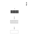
  • FIG. 92 contains a layer legend for the A-labeled (i.e., 1 A, 2 A, 3 A, etc.) figures;
  • FIG. 93 contains a layer legend the B-labeled figures.
  • FIG. 94 contains a layer legend for the C-labeled figures.
  • FIGS. 92-94 show layer maps for the respective A-labeled, B-labeled and C-labeled figures that follow.
  • the full set of depicted layers includes: M0 (first metal), NW (N-well), TS (trench silicide), RX (active), CA (contact to active), PC (gate, a/k/a polysilicon or poly—although the gate material in advanced processes is typically metallic), GO (gate open, a/k/a CB), V0 (via to interconnect), and M1 (first-level interconnect).
  • any of these layers may be created through multiple exposure (e.g., double, triple or quadruple patterned) processes, and/or through use of cut masks, which themselves may be multi-patterned.
  • the A-labeled figures in this application are intended to show the resulting complete cells as clearly as possible; thus, the details of multi-patterning and cut-masking have been eliminated from these figures.
  • FIGs. 93 and 94 show the layer maps for the B-labeled and C-labeled figures, which depict the multi-patterning, cut-masked details of M0 patterning in the inventive cells.
  • M0 is patterned in two exposures (M0_color1 and M0_color2), each of which is patterned by its own cut mask (M0CUT1 and M0CUT2, respectively).
  • PC is shown in both the A-labeled and B-labeled figures as a measurement reference.
  • M0 may be triple patterned, with a separate cut mask for each exposure, and/or an additional cut mask may be provided that cuts both (or all) exposures of M0.
  • FIGS. 1A-C depict an sdffqx1_alt cell.
  • This cell implements the logic function of a scan-enabled, D flip-flop, in drive strength 1.
  • This cell is an example of a state-of-the-art layout that, nevertheless, does not meet the objects of the present invention.
  • CPP contacted poly pitch
  • FIG. 1B one can see that CPP (contacted poly pitch) can be equivalently measured as the left-edge-to-left-edge distance, center-to-center distance, or right-edge-to-right-edge distance between adjacent gate stripes.
  • this cell contains several undesirable configurations in the first-exposure M0 layer: two instances of left-edge-to-left-edge first-exposure M0 cuts with spacing ( 1 and 3 ) of less than 2 ⁇ CPP; and an instance of right-edge-to-right-edge first-exposure M0 cuts with a spacing ( 2 ) of less than 2 ⁇ CPP. (Note, there may be additional violations on this layout, and others that follow in FIGS. 1C and 2B -C. The flagged examples are intended to be exemplary, not exhaustive.) Referring now to FIG.
  • additional undesirable configurations in the second-exposure M0 layer are flagged: an instance of left-edge-to-left-edge second-exposure M0 cuts with a spacing ( 4 ) of less than 2 ⁇ CPP; and an instance of right-edge-to-right-edge second-exposure M0 cuts with a spacing ( 5 ) of less than 2 ⁇ CPP.
  • FIGS. 2A-C depict a mux2x1_alt cell.
  • This cell implements the logic function of a 2-input MUX, in drive strength 1.
  • This cell is another example of a state-of-the-art layout that, nevertheless, does not meet the DFM objects of the present invention.
  • this cell contains undesirable spacings between cuts in the first-exposure M0 layer (see 7 on FIG. 2B ) and between cuts in the second-exposure M0 layer (see 8 and 9 in FIG. 2C ).
  • FIGS. 3A-C contain examples of cells that meet the DFM objects of the present invention, and collectively comprise the exemplary, inventive library herein.
  • FIGS. 3A-C depict an an2x1 cell.
  • This cell implements the logic function of a 2-input AND, in drive strength 1.
  • This cell is 4 CPP wide.
  • FIGS. 4A-C depict an an2x2 cell.
  • This cell implements the logic function of a 2-input AND, in drive strength 2.
  • This cell is 5 CPP wide.
  • FIGS. 5A-C depict an an3x1 cell.
  • This cell implements the logic function of a 3-input AND, in drive strength 1.
  • This cell is 6 CPP wide.
  • FIGS. 6A-C depict an an3x2 cell.
  • This cell implements the logic function of a 3-input AND, in drive strength 2.
  • This cell is 7 CPP wide.
  • FIGS. 7A-C depict an an4x1 cell.
  • This cell implements the logic function of a 4-input AND, in drive strength 1.
  • This cell is 7 CPP wide.
  • FIGS. 8A-C depict an an4x2 cell.
  • This cell implements the logic function of a 4-input AND, in drive strength 2.
  • This cell is 8 CPP wide.
  • FIGS. 9A-C depict an ao21x1 cell.
  • This cell implements the logic function OR(AND(a,b),c), in drive strength 1.
  • This cell is 6 CPP wide.
  • FIGS. 10A-C depict an ao31x1 cell.
  • This cell implements the logic function OR(AND(a,b,c),d), in drive strength 1.
  • This cell is 7 CPP wide.
  • FIGS. 11A-C depict an ao211x1 cell.
  • This cell implements the logic function OR(AND(a,b),c,d), in drive strength 1.
  • This cell is 7 CPP wide.
  • FIGS. 12A-C depict an aoi21x1 cell.
  • This cell implements the logic function NOT(OR(AND(a,b),c)), in drive strength 1.
  • This cell is 4 CPP wide.
  • FIGS. 13A-C depict an aoi21x2 cell.
  • This cell implements the logic function NOT(OR(AND(a,b),c)), in drive strength 2.
  • This cell is 7 CPP wide.
  • FIGS. 14A-C depict an aoi22x1 cell.
  • This cell implements the logic function NOT(OR(AND(a,b),AND(c,d))), in drive strength 1.
  • This cell is 5 CPP wide.
  • FIGS. 15A-C depict an aoi22x2 cell.
  • This cell implements the logic function NOT(OR(AND(a,b),AND(c,d))), in drive strength 2.
  • This cell is 9 CPP wide.
  • FIGS. 16A-C depict an aoi31x1 cell.
  • This cell implements the logic function NOT(OR(AND(a,b,c),d)), in drive strength 1.
  • This cell is 5 CPP wide.
  • FIGS. 17A-C depict an aoi31x2 cell.
  • This cell implements the logic function NOT(OR(AND(a,b,c),d)), in drive strength 2.
  • This cell is 9 CPP wide.
  • FIGS. 18A-C depict an aoi211x1 cell.
  • This cell implements the logic function NOT(OR(AND(a,b),c,d)), in drive strength 1.
  • This cell is 5 CPP wide.
  • FIGS. 19A-C depict an aoi222x1 cell.
  • This cell implements the logic function NOT(OR(AND(a,b),AND(c,d),AND(e,f))), in drive strength 1.
  • This cell is 9 CPP wide.
  • FIGS. 20A-C depict an bufhx6 cell.
  • This cell implements the logic function of a buffer, in drive strength 6.
  • This cell is 10 CPP wide.
  • FIGS. 21A-C depict an bufx1 cell.
  • This cell implements the logic function of a buffer, in drive strength 1.
  • This cell is 3 CPP wide.
  • FIGS. 22A-C depict an bufx2 cell.
  • This cell implements the logic function of a buffer, in drive strength 2.
  • This cell is 4 CPP wide.
  • FIGS. 23A-C depict an bufx3 cell.
  • This cell implements the logic function of a buffer, in drive strength 3.
  • This cell is 5 CPP wide.
  • FIGS. 24A-C depict an bufx4 cell.
  • This cell implements the logic function of a buffer, in drive strength 4.
  • This cell is 7 CPP wide.
  • FIGS. 25A-C depict an bufx6 cell.
  • This cell implements the logic function of a buffer, in drive strength 6.
  • This cell is 9 CPP wide.
  • FIGS. 26A-C depict an bufx8 cell.
  • This cell implements the logic function of a buffer, in drive strength 8.
  • This cell is 12 CPP wide.
  • FIGS. 27A-C depict an ckor21ban2x1 cell.
  • This cell implements the logic function of a clock-gating latch, in drive strength 1.
  • This cell is 17 CPP wide.
  • FIGS. 28A-C depict an dlyx1 cell.
  • This cell implements the logic function of a delay gate, in drive strength 1.
  • This cell is 9 CPP wide.
  • FIGS. 29A-C depict an fax1 cell.
  • This cell implements the logic function of a full adder, in drive strength 1.
  • This double-height cell is 10 CPP wide.
  • FIGS. 30A-C depict an hax1 cell. This cell implements the logic function of a half adder, in drive strength 1. This double-height cell is 8 CPP wide.
  • FIGS. 31A-C depict an iaoi21x1 cell.
  • This cell implements the logic function NOT(OR(AND(a,b),c)), with one of the inputs inverted, in drive strength 1.
  • This cell is 5 CPP wide.
  • FIGS. 32A-C depict an ind2x1 cell.
  • This cell implements the logic function of a 2-input NAND, with one of the inputs inverted, in drive strength 1.
  • This cell is 4 CPP wide.
  • FIGS. 33A-C depict an ind2x2 cell.
  • This cell implements the logic function of a 2-input NAND, with one of the inputs inverted, in drive strength 2.
  • This cell is 6 CPP wide.
  • FIGS. 34A-C depict an ind3x1 cell.
  • This cell implements the logic function of a 3-input NAND, with one of the inputs inverted, in drive strength 1.
  • This cell is 5 CPP wide.
  • FIGS. 35A-C depict an ind3x2 cell.
  • This cell implements the logic function of a 3-input NAND, with one of the inputs inverted, in drive strength 2.
  • This cell is 8 CPP wide.
  • FIGS. 36A-C depict an inr2x1 cell.
  • This cell implements the logic function of a 2-input NOR, with one of the inputs inverted, in drive strength 1.
  • This cell is 4 CPP wide.
  • FIGS. 37A-C depict an inr2x2 cell.
  • This cell implements the logic function of a 2-input NOR, with one of the inputs inverted, in drive strength 2.
  • This cell is 6 CPP wide.
  • FIGS. 38A-C depict an inr3x1 cell.
  • This cell implements the logic function of a 3-input NOR, with one of the inputs inverted, in drive strength 1.
  • This cell is 5 CPP wide.
  • FIGS. 39A-C depict an inr3x2 cell.
  • This cell implements the logic function of a 3-input NOR, with one of the inputs inverted, in drive strength 2.
  • This cell is 8 CPP wide.
  • FIGS. 40A-C depict an invx1 cell.
  • This cell implements the logic function of an inverter, in drive strength 1.
  • This cell is 2 CPP wide.
  • FIGS. 41A-C depict an invx2 cell.
  • This cell implements the logic function of an inverter, in drive strength 2.
  • This cell is 3 CPP wide.
  • FIGS. 42A-C depict an invx4 cell.
  • This cell implements the logic function of an inverter, in drive strength 4.
  • This cell is 5 CPP wide.
  • FIGS. 43A-C depict an invx6 cell.
  • This cell implements the logic function of an inverter, in drive strength 6.
  • This cell is 7 CPP wide.
  • FIGS. 44A-C depict an invx8 cell.
  • This cell implements the logic function of an inverter, in drive strength 8.
  • This cell is 9 CPP wide.
  • FIGS. 45A-C depict an ioai21x1 cell.
  • This cell implements the logic function NOT(AND(OR(a,b),c)), with one of the inputs inverted, in drive strength 1.
  • This cell is 5 CPP wide.
  • FIGS. 46A-C depict an latqx1 cell. This cell implements the logic function of a latch, in drive strength 1. This cell is 13 CPP wide.
  • FIGS. 47A-C depict an mux2x1 cell.
  • This cell implements the logic function of a 2-input MUX, in drive strength 1.
  • This cell is 9 CPP wide.
  • FIGS. 48A-C depict an mux2x2 cell.
  • This cell implements the logic function of a 2-input MUX, in drive strength 2.
  • This cell is 9 CPP wide.
  • FIGS. 49A-C depict an muxi2x1 cell.
  • This cell implements the logic function of a 2-input MUX, with one of its inputs inverted, in drive strength 1.
  • This cell is 7 CPP wide.
  • FIGS. 50A-C depict an nd2x1 cell.
  • This cell implements the logic function of a 2-input NAND, in drive strength 1.
  • This cell is 3 CPP wide.
  • FIGS. 51A-C depict an nd2x2 cell.
  • This cell implements the logic function of a 2-input NAND, in drive strength 2.
  • This cell is 5 CPP wide.
  • FIGS. 52A-C depict an nd2x3 cell.
  • This cell implements the logic function of a 2-input NAND, in drive strength 3.
  • This cell is 7 CPP wide.
  • FIGS. 53A-C depict an nd2x4 cell.
  • This cell implements the logic function of a 2-input NAND, in drive strength 4.
  • This cell is 9 CPP wide.
  • FIGS. 54A-C depict an nd3x1 cell.
  • This cell implements the logic function of a 3-input NAND, in drive strength 1.
  • This cell is 4 CPP wide.
  • FIGS. 55A-C depict an nd3x2 cell.
  • This cell implements the logic function of a 3-input NAND, in drive strength 2.
  • This cell is 7 CPP wide.
  • FIGS. 56A-C depict an nd3x3 cell.
  • This cell implements the logic function of a 3-input NAND, in drive strength 3.
  • This cell is 10 CPP wide.
  • FIGS. 57A-C depict an nd3x4 cell.
  • This cell implements the logic function of a 3-input NAND, in drive strength 4.
  • This cell is 13 CPP wide.
  • FIGS. 58A-C depict an nd4x1 cell.
  • This cell implements the logic function of a 4-input NAND, in drive strength 1.
  • This cell is 5 CPP wide.
  • FIGS. 59A-C depict an nd4x2 cell.
  • This cell implements the logic function of a 4-input NAND, in drive strength 2.
  • This cell is 9 CPP wide.
  • FIGS. 60A-C depict an nr2x1 cell.
  • This cell implements the logic function of a 2-input NOR, in drive strength 1.
  • This cell is 3 CPP wide.
  • FIGS. 61A-C depict an nr2x2 cell.
  • This cell implements the logic function of a 2-input NOR, in drive strength 2.
  • This cell is 5 CPP wide.
  • FIGS. 61.1A-C depict an nr2x3 cell.
  • This cell implements the logic function of a 2-input NOR, in drive strength 3.
  • This cell is 7 CPP wide.
  • FIGS. 62A-C depict an nr2x4 cell.
  • This cell implements the logic function of a 2-input NOR, in drive strength 4.
  • This cell is 9 CPP wide.
  • FIGS. 63A-C depict an nr3x1 cell.
  • This cell implements the logic function of a 3-input NOR, in drive strength 1.
  • This cell is 4 CPP wide.
  • FIGS. 64A-C depict an nr3x2 cell.
  • This cell implements the logic function of a 3-input NOR, in drive strength 2.
  • This cell is 7 CPP wide.
  • FIGS. 65A-C depict an nr3x3 cell.
  • This cell implements the logic function of a 3-input NOR, in drive strength 3.
  • This cell is 10 CPP wide.
  • FIGS. 66A-C depict an nr3x4 cell.
  • This cell implements the logic function of a 3-input NOR, in drive strength 4.
  • This cell is 13 CPP wide.
  • FIGS. 67A-C depict an nr4x1 cell.
  • This cell implements the logic function of a 4-input NOR, in drive strength 1.
  • This cell is 5 CPP wide.
  • FIGS. 68A-C depict an nr4x2 cell.
  • This cell implements the logic function of a 4-input NOR, in drive strength 2.
  • This cell is 9 CPP wide.
  • FIGS. 69A-C depict an oa21x1 cell.
  • This cell implements the logic function AND(OR(a,b),c), in drive strength 1.
  • This cell is 6 CPP wide.
  • FIGS. 70A-C depict an oa31x1 cell. This cell implements the logic function AND(OR(a,b,c),d), in drive strength 1. This cell is 7 CPP wide.
  • FIGS. 71A-C depict an oa211x1 cell.
  • This cell implements the logic function AND(OR(a,b),c,d), in drive strength 1.
  • This cell is 7 CPP wide.
  • FIGS. 72A-C depict an oai21x1 cell.
  • This cell implements the logic function NOT(AND(OR(a,b),c)), in drive strength 1.
  • This cell is 4 CPP wide.
  • FIGS. 73A-C depict an oai21x2 cell.
  • This cell implements the logic function NOT(AND(OR(a,b),c)), in drive strength 2.
  • This cell is 7 CPP wide.
  • FIGS. 74A-C depict an oai22x1 cell.
  • This cell implements the logic function NOT(AND(OR(a,b),OR(c,d)), in drive strength 1.
  • This cell is 5 CPP wide.
  • FIGS. 75A-C depict an oai22x2 cell.
  • This cell implements the logic function NOT(AND(OR(a,b),OR(c,d)), in drive strength 2.
  • This cell is 9 CPP wide.
  • FIGS. 76A-C depict an oai31x1 cell.
  • This cell implements the logic function NOT(AND(OR(a,b,c),d)), in drive strength 1.
  • This cell is 5 CPP wide.
  • FIGS. 77A-C depict an oai31x2 cell.
  • This cell implements the logic function NOT(AND(OR(a,b,c),d)), in drive strength 2.
  • This cell is 9 CPP wide.
  • FIGS. 78A-C depict an oai211x1 cell.
  • This cell implements the logic function NOT(AND(OR(a,b),c,d)), in drive strength 1.
  • This cell is 5 CPP wide.
  • FIGS. 79A-C depict an oai222x1 cell.
  • This cell implements the logic function NOT(AND(OR(a,b),OR(c,d),OR(e,f))), in drive strength 1.
  • This cell is 9 CPP wide.
  • FIGS. 80A-C depict an or2x1 cell.
  • This cell implements the logic function of a 2-input OR, in drive strength 1.
  • This cell is 4 CPP wide.
  • FIGS. 81A-C depict an or2x2 cell.
  • This cell implements the logic function of a 2-input OR, in drive strength 2.
  • This cell is 5 CPP wide.
  • FIGS. 82A-C depict an or3x1 cell.
  • This cell implements the logic function of a 3-input OR, in drive strength 1.
  • This cell is 6 CPP wide.
  • FIGS. 83A-C depict an or3x2 cell.
  • This cell implements the logic function of a 3-input OR, in drive strength 2.
  • This cell is 7 CPP wide.
  • FIGS. 84A-C depict an or4x1 cell.
  • This cell implements the logic function of a 4-input OR, in drive strength 1.
  • This cell is 7 CPP wide.
  • FIGS. 85A-C depict an or4x2 cell.
  • This cell implements the logic function of a 4-input OR, in drive strength 2.
  • This cell is 8 CPP wide.
  • FIGS. 86A-C depict an sdffqx1 cell.
  • This cell implements the logic function of a scan-enabled D flip-flop, in drive strength 1.
  • This double-height cell is 13 CPP wide.
  • FIGS. 87A-C depict an sdffrsqx1 cell.
  • This cell implements the logic function of a scan-enabled D flip-flop, with set and reset, in drive strength 1.
  • This double-height cell is 17 CPP wide.
  • FIGS. 88A-C depict an tiehix1 cell.
  • This cell implements the logic function 1, in drive strength 1.
  • This cell is 3 CPP wide.
  • FIGS. 89A-C depict an tielox1 cell.
  • This cell implements the logic function 0, in drive strength 1.
  • This cell is 3 CPP wide.
  • FIGS. 90A-C depict an xnr2x1 cell.
  • This cell implements the logic function of a 2-input XNOR, in drive strength 1.
  • This cell is 11 CPP wide.
  • FIGS. 91A-C depict an xor2x1 cell.
  • This cell implements the logic function of a 2-input XOR, in drive strength 1.
  • This cell is 11 CPP wide.

Landscapes

  • Engineering & Computer Science (AREA)
  • Computer Hardware Design (AREA)
  • Physics & Mathematics (AREA)
  • General Engineering & Computer Science (AREA)
  • Theoretical Computer Science (AREA)
  • Evolutionary Computation (AREA)
  • Geometry (AREA)
  • General Physics & Mathematics (AREA)
  • Logic Circuits (AREA)

Abstract

A library of a DFM-improved standard logic cells that avoid pattern-degrading configurations in the M0 layer is disclosed, along with wafers, chips and systems constructed from such cells.

Description

A portion of the disclosure of this patent document contains material which is subject to mask work protection, *M*, PDF Solutions, Inc. The mask work owner (PDF Solutions, Inc.) has no objection to the facsimile reproduction by anyone of the patent document or the patent disclosure, as it appears in the Patent and Trademark Office patent file or records, but otherwise reserves all mask work rights whatsoever.
FIELD OF THE INVENTION
This invention relates to design for manufacturability (DFM) of standard cells for advanced semiconductor processes (e.g., 10 nm, 7 nm), to libraries containing such cells, and to wafers/chips that contain instances of such cells.
BACKGROUND OF THE INVENTION
As semiconductor processes advance to render increasingly smaller features, the design of dense, high-yielding (manufacturable) cells becomes increasingly challenging. See, e.g., U.S. Pat. No. 9,202,820, “Flip-flop, latch, and mux cells for use in a standard cell library and integrated circuits made therefrom,” to the inventor herein.
In the most advanced processes, patterning of critical layers is typically restricted to one direction (unidirectional) in each layer, delimited by cut masks, with the cut masks increasingly multi-patterned. In such technologies, careful attention to often non-obvious potential manufacturability problems is critical to successful implementation of a standard cell library. The invention, as described in detail below, provides an example of a DFM-optimized standard cell library for use in such advanced semiconductor processes.
SUMMARY OF THE INVENTION
One aspect relates to a library of DFM-improved standard cells, optimized for use in advanced semiconductor processes that include multi-patterned M0 cut masks.
Another aspect of the invention relates to wafers, chips, and systems that include such DFM-improved cells.
Applicant has discovered that, with very careful design, seemingly incompatible demands for cell density and avoidance of certain difficult-to-manufacture features can be simultaneously achieved. In particular, as exemplified by the depicted cells herein, the present invention provides a library of competitively dense logic cells with highly-optimized patterning in the first-level metal (M0) layer. As described in greater detail below, such patterning avoids spacing M0 cuts so close that they increase the risk of manufacturing failure.
Accordingly, generally speaking, and without intending to be limiting, certain aspects of the invention relate to collections of standard logic cells, implementing a plurality of logic functions, wherein each standard cell comprises, for example, at least the following: two elongated supply rails, each formed in a first metal (M0) layer, each supply rail having a width at least twice a minimum permitted width for M0 features, and each supply rail extending horizontally across the entire width of the standard cell; at least three elongated gate stripes, each formed in a gate (PC) layer, and each extending vertically between at least two of the supply rails, with adjacent gate stripes spaced at a minimum contacted poly pitch (CPP); positioned vertically between the supply rails, at least two, first-exposure M0 tracks, each of the first-exposure M0 tracks having the minimum permitted width and extending horizontally across the cell, the first-exposure M0 tracks patterned, in part, by portion(s) of a first-exposure M0 mask (M0_color1) and, in part, by portion(s) of a first-exposure M0 cut mask (M0CUT1); positioned vertically between the supply rails, at least two, second-exposure M0 tracks, each of the second-exposure M0 tracks having the minimum permitted width and extending horizontally across the cell, the second-exposure M0 tracks patterned, in part, by portion(s) of a second-exposure M0 mask (M0_color2) and, in part, by portion(s) of a second-exposure M0 cut mask (M0CUT2); and additional patterned features, in NW (N-well), TS (trench silicide), RX (active), CA (contact to active), GO (gate open, a/k/a CB), V0 (via to interconnect), and M1 (first-level interconnect) layers, configured to realize a logical function or behavior of the standard cell; wherein within in the cell: all M0CUT1 features are rectangular in shape, with a left edge, right edge, top edge, and bottom edge, and as between any two first and second M0CUT1 features within the cell, there is at least 2×CPP of spacing between all points at which the left edge of the first M0CUT1 feature intersects an M0color1 feature and all points at which the left edge of the second M0CUT1 feature intersects an M0color1 feature, and there is at least 2×CPP of spacing between all points at which the right edge of the first M0CUT1 feature intersects an M0color1 feature and all points at which the right edge of the second M0CUT1 feature intersects an M0color1 feature; and all M0CUT2 features are rectangular in shape, with a left edge, right edge, top edge, and bottom edge, and as between any two first and second M0CUT2 features within the cell, there is at least 2×CPP of spacing between all points at which the left edge of the first M0CUT2 feature intersects an M0color2 feature and all points at which the left edge of the second M0CUT2 feature intersects an M0color2 feature, and there is at least 2×CPP of spacing between all points at which the right edge of the first M0CUT2 feature intersects an M0color2 feature and all points at which the right edge of the second M0CUT2 feature intersects an M0color2 feature. Such collections may be embodied on silicon wafers, chips, or systems, or as instructions for patterning such cells, where such instruction are contained in a non-transient, computer-readable mediums, in data formats such as GDSII. Such collections preferably include cells implementing at least four, six, eight, ten, twelve, fourteen, sixteen, eighteen, twenty or more logical functions selected from the following list, each of which may be provided in multiple drive strength variants:
    • 1. the logic function of a 2-input AND;
    • 2. the logic function of a 3-input AND;
    • 3. the logic function of a 4-input AND;
    • 4. the logic function OR(AND(a,b),c);
    • 5. the logic function OR(AND(a,b,c),d);
    • 6. the logic function OR(AND(a,b),c,d);
    • 7. the logic function NOT(OR(AND(a,b),c));
    • 8. the logic function NOT(OR(AND(a,b),AND(c,d)));
    • 9. the logic function NOT(OR(AND(a,b,c),d));
    • 10. the logic function NOT(OR(AND(a,b),c,d));
    • 11. the logic function NOT(OR(AND(a,b),AND(c,d),AND(e,f)));
    • 12. the logic function of a buffer;
    • 13. the logic function of a clock-gating latch;
    • 14. the logic function of a delay gate;
    • 15. the logic function of a full adder;
    • 16. the logic function of a half adder;
    • 17. the logic function NOT(OR(AND(a,b),c)), with one of its inputs inverted;
    • 18. the logic function of a 2-input NAND, with one of its inputs inverted;
    • 19. the logic function of a 3-input NAND, with one of its inputs inverted;
    • 20. the logic function of a 2-input NOR, with one of its inputs inverted;
    • 21. the logic function of a 3-input NOR, with one of its inputs inverted;
    • 22. the logic function of an inverter;
    • 23. the logic function NOT(AND(OR(a,b),c)), with one of its inputs inverted;
    • 24. the logic function of a latch;
    • 25. the logic function of a 2-input MUX;
    • 26. the logic function of a 2-input MUX, with one of its inputs inverted;
    • 27. the logic function of a 2-input NAND;
    • 28. the logic function of a 3-input NAND;
    • 29. the logic function of a 4-input NAND;
    • 30. the logic function of a 2-input NOR;
    • 31. the logic function of a 3-input NOR;
    • 32. the logic function of a 4-input NOR;
    • 33. the logic function AND(OR(a,b),c);
    • 34. the logic function AND(OR(a,b,c),d);
    • 35. the logic function AND(OR(a,b),c,d);
    • 36. the logic function NOT(AND(OR(a,b),c));
    • 37. the logic function NOT(AND(OR(a,b),OR(c,d));
    • 38. the logic function NOT(AND(OR(a,b,c),d));
    • 39. the logic function NOT(AND(OR(a,b),c,d));
    • 40. the logic function NOT(AND(OR(a,b),OR(c,d),OR(e,f)));
    • 41. the logic function of a 2-input OR;
    • 42. the logic function of a 3-input OR;
    • 43. the logic function of a 4-input OR;
    • 44. the logic function of a scan-enabled D flip-flop;
    • 45. the logic function of a scan-enabled D flip-flop, with set and reset;
    • 46. the logic function 1;
    • 47. the logic function 0;
    • 48. the logic function of a 2-input XNOR; and,
    • 49. the logic function of a 2-input XOR.
Again, generally speaking, and without intending to be limiting, other aspects of the invention relate to collections of standard logic cells, implementing a plurality of logic functions, wherein each standard cell comprises, for example, at least the following: at least two elongated supply rails, extending horizontally across the standard cell; at least three elongated gate stripes, each extending vertically between at least two of said supply rails, adjacent gate stripes spaced at a minimum contacted poly pitch (CPP); positioned vertically between the supply rails, one or more first-exposure M0 tracks, each of the first-exposure M0 tracks having a minimum permitted width for M0 patterning and extending horizontally across the cell, the first-exposure M0 tracks patterned, in part, by feature(s) of a first-exposure M0 mask (M0_color1) and, in part, by feature(s) of a first-exposure M0 cut mask (M0CUT1); positioned vertically between the supply rails, one or more second-exposure M0 tracks, each of the second-exposure M0 tracks having the minimum permitted width and extending horizontally across the cell, the second-exposure M0 tracks patterned, in part, by feature(s) of a second-exposure M0 mask (M0_color2) and, in part, by feature(s) of a second-exposure M0 cut mask (M0CUT2); and means, including additional patterned features in NW (N-well), TS (trench silicide), RX (active), CA (contact to active), GO (gate open), V0 (via to interconnect), and M1 (first-level interconnect) layers, configured to realize a logical function or behavior of the standard cell; and wherein within in the cell: all M0CUT1 features are rectangular in shape, with a left edge, right edge, top edge, and bottom edge, and as between any two first and second M0CUT1 features within the cell, there is at least 2×CPP of spacing between all points at which the left edge of the first M0CUT1 feature intersects an M0color1 feature and all points at which the left edge of the second M0CUT1 feature intersects an M0color1 feature, and there is at least 2×CPP of spacing between all points at which the right edge of the first M0CUT1 feature intersects an M0color1 feature and all points at which the right edge of the second M0CUT1 feature intersects an M0color1 feature; and all M0CUT2 features are rectangular in shape, with a left edge, right edge, top edge, and bottom edge, and as between any two first and second M0CUT2 features within the cell, there is at least 2×CPP of spacing between all points at which the left edge of the first M0CUT2 feature intersects an M0color2 feature and all points at which the left edge of the second M0CUT2 feature intersects an M0color2 feature, and there is at least 2×CPP of spacing between all points at which the right edge of the first M0CUT2 feature intersects an M0color2 feature and all points at which the right edge of the second M0CUT2 feature intersects an M0color2 feature.
BRIEF DESCRIPTION OF THE DRAWINGS
The above, as well as other, aspects, features and advantages of the present invention are illustrated in the accompanying set of figures, which are rendered to relative scale, and in which:
FIGS. 1A-C depict an sdffqx1_alt cell;
FIGS. 2A-C depict a mux2x1_alt cell;
FIGS. 3A-C depict an an2x1 cell;
FIGS. 4A-C depict an an2x2 cell;
FIGS. 5A-C depict an an3x1 cell;
FIGS. 6A-C depict an an3x2 cell;
FIGS. 7A-C depict an an4x1 cell;
FIGS. 8A-C depict an an4x2 cell;
FIGS. 9A-C depict an ao21x1 cell;
FIGS. 10A-C depict an ao31x1 cell;
FIGS. 11A-C depict an ao211x1 cell;
FIGS. 12A-C depict an aoi21x1 cell;
FIGS. 13A-C depict an aoi21x2 cell;
FIGS. 14A-C depict an aoi22x1 cell;
FIGS. 15A-C depict an aoi22x2 cell;
FIGS. 16A-C depict an aoi31x1 cell;
FIGS. 17A-C depict an aoi31x2 cell;
FIGS. 18A-C depict an aoi211x1 cell;
FIGS. 19A-C depict an aoi222x1 cell;
FIGS. 20A-C depict an bufhx6 cell;
FIGS. 21A-C depict an bufx1 cell;
FIGS. 22A-C depict an bufx2 cell;
FIGS. 23A-C depict an bufx3 cell;
FIGS. 24A-C depict an bufx4 cell;
FIGS. 25A-C depict an bufx6 cell;
FIGS. 26A-C depict an bufx8 cell;
FIGS. 27A-C depict an ckor21ban2x1 cell;
FIGS. 28A-C depict an dlyx1 cell;
FIGS. 29A-C depict an fax1 cell;
FIGS. 30A-C depict an hax1 cell;
FIGS. 31A-C depict an iaoi21x1 cell;
FIGS. 32A-C depict an ind2x1 cell;
FIGS. 33A-C depict an ind2x2 cell;
FIGS. 34A-C depict an ind3x1 cell;
FIGS. 35A-C depict an ind3x2 cell;
FIGS. 36A-C depict an inr2x1 cell;
FIGS. 37A-C depict an inr2x2 cell;
FIGS. 38A-C depict an inr3x1 cell;
FIGS. 39A-C depict an inr3x2 cell;
FIGS. 40A-C depict an invx1 cell;
FIGS. 41A-C depict an invx2 cell;
FIGS. 42A-C depict an invx4 cell;
FIGS. 43A-C depict an invx6 cell;
FIGS. 44A-C depict an invx8 cell;
FIGS. 45A-C depict an ioai21x1 cell;
FIGS. 46A-C depict an latqx1 cell;
FIGS. 47A-C depict an mux2x1 cell;
FIGS. 48A-C depict an mux2x2 cell;
FIGS. 49A-C depict an muxi2x1 cell;
FIGS. 50A-C depict an nd2x1 cell;
FIGS. 51A-C depict an nd2x2 cell;
FIGS. 52A-C depict an nd2x3 cell;
FIGS. 53A-C depict an nd2x4 cell;
FIGS. 54A-C depict an nd3x1 cell;
FIGS. 55A-C depict an nd3x2 cell;
FIGS. 56A-C depict an nd3x3 cell;
FIGS. 57A-C depict an nd3x4 cell;
FIGS. 58A-C depict an nd4x1 cell;
FIGS. 59A-C depict an nd4x2 cell;
FIGS. 60A-C depict an nr2x1 cell;
FIGS. 61A-C depict an nr2x2 cell;
FIGS. 61.1A-C depict an nr2x3 cell;
FIGS. 62A-C depict an nr2x4 cell;
FIGS. 63A-C depict an nr3x1 cell;
FIGS. 64A-C depict an nr3x2 cell;
FIGS. 65A-C depict an nr3x3 cell;
FIGS. 66A-C depict an nr3x4 cell;
FIGS. 67A-C depict an nr4x1 cell;
FIGS. 68A-C depict an nr4x2 cell;
FIGS. 69A-C depict an oa21x1 cell;
FIGS. 70A-C depict an oa31x1 cell;
FIGS. 71A-C depict an oa211x1 cell;
FIGS. 72A-C depict an oai21x1 cell;
FIGS. 73A-C depict an oai21x2 cell;
FIGS. 74A-C depict an oai22x1 cell;
FIGS. 75A-C depict an oai22x2 cell;
FIGS. 76A-C depict an oai31x1 cell;
FIGS. 77A-C depict an oai31x2 cell;
FIGS. 78A-C depict an oai211x1 cell;
FIGS. 79A-C depict an oai222x1 cell;
FIGS. 80A-C depict an or2x1 cell;
FIGS. 81A-C depict an or2x2 cell;
FIGS. 82A-C depict an or3x1 cell;
FIGS. 83A-C depict an or3x2 cell;
FIGS. 84A-C depict an or4x1 cell;
FIGS. 85A-C depict an or4x2 cell;
FIGS. 86A-C depict an sdffqx1 cell;
FIGS. 87A-C depict an sdffrsqx1 cell;
FIGS. 88A-C depict an tiehix1 cell;
FIGS. 89A-C depict an tielox1 cell;
FIGS. 90A-C depict an xnr2x1 cell; and,
FIGS. 91A-C depict an xor2x1 cell.
FIG. 92 contains a layer legend for the A-labeled (i.e., 1A, 2A, 3A, etc.) figures;
FIG. 93 contains a layer legend the B-labeled figures; and,
FIG. 94 contains a layer legend for the C-labeled figures;.
DESCRIPTION OF EXEMPLARY EMBODIMENT(S)
FIGS. 92-94 show layer maps for the respective A-labeled, B-labeled and C-labeled figures that follow. With reference to FIG. 92, the full set of depicted layers includes: M0 (first metal), NW (N-well), TS (trench silicide), RX (active), CA (contact to active), PC (gate, a/k/a polysilicon or poly—although the gate material in advanced processes is typically metallic), GO (gate open, a/k/a CB), V0 (via to interconnect), and M1 (first-level interconnect). Persons skilled in the art will appreciate that any of these layers may be created through multiple exposure (e.g., double, triple or quadruple patterned) processes, and/or through use of cut masks, which themselves may be multi-patterned. The A-labeled figures in this application are intended to show the resulting complete cells as clearly as possible; thus, the details of multi-patterning and cut-masking have been eliminated from these figures.
Referring now to FIGs. 93 and 94, these show the layer maps for the B-labeled and C-labeled figures, which depict the multi-patterning, cut-masked details of M0 patterning in the inventive cells. In particular, in the exemplary embodiment herein, M0 is patterned in two exposures (M0_color1 and M0_color2), each of which is patterned by its own cut mask (M0CUT1 and M0CUT2, respectively). PC is shown in both the A-labeled and B-labeled figures as a measurement reference. Persons skilled in the art will understand that variations on the M0 process are possible. For example, M0 may be triple patterned, with a separate cut mask for each exposure, and/or an additional cut mask may be provided that cuts both (or all) exposures of M0.
Reference is now made to FIGS. 1A-C, which depict an sdffqx1_alt cell. This cell implements the logic function of a scan-enabled, D flip-flop, in drive strength 1. This cell is an example of a state-of-the-art layout that, nevertheless, does not meet the objects of the present invention. Referring first to FIG. 1B, one can see that CPP (contacted poly pitch) can be equivalently measured as the left-edge-to-left-edge distance, center-to-center distance, or right-edge-to-right-edge distance between adjacent gate stripes. As further depicted in FIG. 1B, this cell contains several undesirable configurations in the first-exposure M0 layer: two instances of left-edge-to-left-edge first-exposure M0 cuts with spacing (1 and 3) of less than 2×CPP; and an instance of right-edge-to-right-edge first-exposure M0 cuts with a spacing (2) of less than 2×CPP. (Note, there may be additional violations on this layout, and others that follow in FIGS. 1C and 2B-C. The flagged examples are intended to be exemplary, not exhaustive.) Referring now to FIG. 1C, additional undesirable configurations in the second-exposure M0 layer are flagged: an instance of left-edge-to-left-edge second-exposure M0 cuts with a spacing (4) of less than 2×CPP; and an instance of right-edge-to-right-edge second-exposure M0 cuts with a spacing (5) of less than 2×CPP.
Reference is now made to FIGS. 2A-C, which depict a mux2x1_alt cell. This cell implements the logic function of a 2-input MUX, in drive strength 1. This cell is another example of a state-of-the-art layout that, nevertheless, does not meet the DFM objects of the present invention. As flagged in FIGS. 2B and 2C, this cell contains undesirable spacings between cuts in the first-exposure M0 layer (see 7 on FIG. 2B) and between cuts in the second-exposure M0 layer (see 8 and 9 in FIG. 2C).
FIGS. 3A-C, et seq., as described below, contain examples of cells that meet the DFM objects of the present invention, and collectively comprise the exemplary, inventive library herein.
Reference is now made to FIGS. 3A-C, which depict an an2x1 cell. This cell implements the logic function of a 2-input AND, in drive strength 1. This cell is 4 CPP wide.
Reference is now made to FIGS. 4A-C, which depict an an2x2 cell. This cell implements the logic function of a 2-input AND, in drive strength 2. This cell is 5 CPP wide.
Reference is now made to FIGS. 5A-C, which depict an an3x1 cell. This cell implements the logic function of a 3-input AND, in drive strength 1. This cell is 6 CPP wide.
Reference is now made to FIGS. 6A-C, which depict an an3x2 cell. This cell implements the logic function of a 3-input AND, in drive strength 2. This cell is 7 CPP wide.
Reference is now made to FIGS. 7A-C, which depict an an4x1 cell. This cell implements the logic function of a 4-input AND, in drive strength 1. This cell is 7 CPP wide.
Reference is now made to FIGS. 8A-C, which depict an an4x2 cell. This cell implements the logic function of a 4-input AND, in drive strength 2. This cell is 8 CPP wide.
Reference is now made to FIGS. 9A-C, which depict an ao21x1 cell. This cell implements the logic function OR(AND(a,b),c), in drive strength 1. This cell is 6 CPP wide.
Reference is now made to FIGS. 10A-C, which depict an ao31x1 cell. This cell implements the logic function OR(AND(a,b,c),d), in drive strength 1. This cell is 7 CPP wide.
Reference is now made to FIGS. 11A-C, which depict an ao211x1 cell. This cell implements the logic function OR(AND(a,b),c,d), in drive strength 1. This cell is 7 CPP wide.
Reference is now made to FIGS. 12A-C, which depict an aoi21x1 cell. This cell implements the logic function NOT(OR(AND(a,b),c)), in drive strength 1. This cell is 4 CPP wide.
Reference is now made to FIGS. 13A-C, which depict an aoi21x2 cell. This cell implements the logic function NOT(OR(AND(a,b),c)), in drive strength 2. This cell is 7 CPP wide.
Reference is now made to FIGS. 14A-C, which depict an aoi22x1 cell. This cell implements the logic function NOT(OR(AND(a,b),AND(c,d))), in drive strength 1. This cell is 5 CPP wide.
Reference is now made to FIGS. 15A-C, which depict an aoi22x2 cell. This cell implements the logic function NOT(OR(AND(a,b),AND(c,d))), in drive strength 2. This cell is 9 CPP wide.
Reference is now made to FIGS. 16A-C, which depict an aoi31x1 cell. This cell implements the logic function NOT(OR(AND(a,b,c),d)), in drive strength 1. This cell is 5 CPP wide.
Reference is now made to FIGS. 17A-C, which depict an aoi31x2 cell. This cell implements the logic function NOT(OR(AND(a,b,c),d)), in drive strength 2. This cell is 9 CPP wide.
Reference is now made to FIGS. 18A-C, which depict an aoi211x1 cell. This cell implements the logic function NOT(OR(AND(a,b),c,d)), in drive strength 1. This cell is 5 CPP wide.
Reference is now made to FIGS. 19A-C, which depict an aoi222x1 cell. This cell implements the logic function NOT(OR(AND(a,b),AND(c,d),AND(e,f))), in drive strength 1. This cell is 9 CPP wide.
Reference is now made to FIGS. 20A-C, which depict an bufhx6 cell. This cell implements the logic function of a buffer, in drive strength 6. This cell is 10 CPP wide.
Reference is now made to FIGS. 21A-C, which depict an bufx1 cell. This cell implements the logic function of a buffer, in drive strength 1. This cell is 3 CPP wide.
Reference is now made to FIGS. 22A-C, which depict an bufx2 cell. This cell implements the logic function of a buffer, in drive strength 2. This cell is 4 CPP wide.
Reference is now made to FIGS. 23A-C, which depict an bufx3 cell. This cell implements the logic function of a buffer, in drive strength 3. This cell is 5 CPP wide.
Reference is now made to FIGS. 24A-C, which depict an bufx4 cell. This cell implements the logic function of a buffer, in drive strength 4. This cell is 7 CPP wide.
Reference is now made to FIGS. 25A-C, which depict an bufx6 cell. This cell implements the logic function of a buffer, in drive strength 6. This cell is 9 CPP wide.
Reference is now made to FIGS. 26A-C, which depict an bufx8 cell. This cell implements the logic function of a buffer, in drive strength 8. This cell is 12 CPP wide.
Reference is now made to FIGS. 27A-C, which depict an ckor21ban2x1 cell. This cell implements the logic function of a clock-gating latch, in drive strength 1. This cell is 17 CPP wide.
Reference is now made to FIGS. 28A-C, which depict an dlyx1 cell. This cell implements the logic function of a delay gate, in drive strength 1. This cell is 9 CPP wide.
Reference is now made to FIGS. 29A-C, which depict an fax1 cell. This cell implements the logic function of a full adder, in drive strength 1. This double-height cell is 10 CPP wide.
Reference is now made to FIGS. 30A-C, which depict an hax1 cell. This cell implements the logic function of a half adder, in drive strength 1. This double-height cell is 8 CPP wide.
Reference is now made to FIGS. 31A-C, which depict an iaoi21x1 cell. This cell implements the logic function NOT(OR(AND(a,b),c)), with one of the inputs inverted, in drive strength 1. This cell is 5 CPP wide.
Reference is now made to FIGS. 32A-C, which depict an ind2x1 cell. This cell implements the logic function of a 2-input NAND, with one of the inputs inverted, in drive strength 1. This cell is 4 CPP wide.
Reference is now made to FIGS. 33A-C, which depict an ind2x2 cell. This cell implements the logic function of a 2-input NAND, with one of the inputs inverted, in drive strength 2. This cell is 6 CPP wide.
Reference is now made to FIGS. 34A-C, which depict an ind3x1 cell. This cell implements the logic function of a 3-input NAND, with one of the inputs inverted, in drive strength 1. This cell is 5 CPP wide.
Reference is now made to FIGS. 35A-C, which depict an ind3x2 cell. This cell implements the logic function of a 3-input NAND, with one of the inputs inverted, in drive strength 2. This cell is 8 CPP wide.
Reference is now made to FIGS. 36A-C, which depict an inr2x1 cell. This cell implements the logic function of a 2-input NOR, with one of the inputs inverted, in drive strength 1. This cell is 4 CPP wide.
Reference is now made to FIGS. 37A-C, which depict an inr2x2 cell. This cell implements the logic function of a 2-input NOR, with one of the inputs inverted, in drive strength 2. This cell is 6 CPP wide.
Reference is now made to FIGS. 38A-C, which depict an inr3x1 cell. This cell implements the logic function of a 3-input NOR, with one of the inputs inverted, in drive strength 1. This cell is 5 CPP wide.
Reference is now made to FIGS. 39A-C, which depict an inr3x2 cell. This cell implements the logic function of a 3-input NOR, with one of the inputs inverted, in drive strength 2. This cell is 8 CPP wide.
Reference is now made to FIGS. 40A-C, which depict an invx1 cell. This cell implements the logic function of an inverter, in drive strength 1. This cell is 2 CPP wide.
Reference is now made to FIGS. 41A-C, which depict an invx2 cell. This cell implements the logic function of an inverter, in drive strength 2. This cell is 3 CPP wide.
Reference is now made to FIGS. 42A-C, which depict an invx4 cell. This cell implements the logic function of an inverter, in drive strength 4. This cell is 5 CPP wide.
Reference is now made to FIGS. 43A-C, which depict an invx6 cell. This cell implements the logic function of an inverter, in drive strength 6. This cell is 7 CPP wide.
Reference is now made to FIGS. 44A-C, which depict an invx8 cell. This cell implements the logic function of an inverter, in drive strength 8. This cell is 9 CPP wide.
Reference is now made to FIGS. 45A-C, which depict an ioai21x1 cell. This cell implements the logic function NOT(AND(OR(a,b),c)), with one of the inputs inverted, in drive strength 1. This cell is 5 CPP wide.
Reference is now made to FIGS. 46A-C, which depict an latqx1 cell. This cell implements the logic function of a latch, in drive strength 1. This cell is 13 CPP wide.
Reference is now made to FIGS. 47A-C, which depict an mux2x1 cell. This cell implements the logic function of a 2-input MUX, in drive strength 1. This cell is 9 CPP wide.
Reference is now made to FIGS. 48A-C, which depict an mux2x2 cell. This cell implements the logic function of a 2-input MUX, in drive strength 2. This cell is 9 CPP wide.
Reference is now made to FIGS. 49A-C, which depict an muxi2x1 cell. This cell implements the logic function of a 2-input MUX, with one of its inputs inverted, in drive strength 1. This cell is 7 CPP wide.
Reference is now made to FIGS. 50A-C, which depict an nd2x1 cell. This cell implements the logic function of a 2-input NAND, in drive strength 1. This cell is 3 CPP wide.
Reference is now made to FIGS. 51A-C, which depict an nd2x2 cell. This cell implements the logic function of a 2-input NAND, in drive strength 2. This cell is 5 CPP wide.
Reference is now made to FIGS. 52A-C, which depict an nd2x3 cell. This cell implements the logic function of a 2-input NAND, in drive strength 3. This cell is 7 CPP wide.
Reference is now made to FIGS. 53A-C, which depict an nd2x4 cell. This cell implements the logic function of a 2-input NAND, in drive strength 4. This cell is 9 CPP wide.
Reference is now made to FIGS. 54A-C, which depict an nd3x1 cell. This cell implements the logic function of a 3-input NAND, in drive strength 1. This cell is 4 CPP wide.
Reference is now made to FIGS. 55A-C, which depict an nd3x2 cell. This cell implements the logic function of a 3-input NAND, in drive strength 2. This cell is 7 CPP wide.
Reference is now made to FIGS. 56A-C, which depict an nd3x3 cell. This cell implements the logic function of a 3-input NAND, in drive strength 3. This cell is 10 CPP wide.
Reference is now made to FIGS. 57A-C, which depict an nd3x4 cell. This cell implements the logic function of a 3-input NAND, in drive strength 4. This cell is 13 CPP wide.
Reference is now made to FIGS. 58A-C, which depict an nd4x1 cell. This cell implements the logic function of a 4-input NAND, in drive strength 1. This cell is 5 CPP wide.
Reference is now made to FIGS. 59A-C, which depict an nd4x2 cell. This cell implements the logic function of a 4-input NAND, in drive strength 2. This cell is 9 CPP wide.
Reference is now made to FIGS. 60A-C, which depict an nr2x1 cell. This cell implements the logic function of a 2-input NOR, in drive strength 1. This cell is 3 CPP wide.
Reference is now made to FIGS. 61A-C, which depict an nr2x2 cell. This cell implements the logic function of a 2-input NOR, in drive strength 2. This cell is 5 CPP wide.
Reference is now made to FIGS. 61.1A-C, which depict an nr2x3 cell. This cell implements the logic function of a 2-input NOR, in drive strength 3. This cell is 7 CPP wide.
Reference is now made to FIGS. 62A-C, which depict an nr2x4 cell. This cell implements the logic function of a 2-input NOR, in drive strength 4. This cell is 9 CPP wide.
Reference is now made to FIGS. 63A-C, which depict an nr3x1 cell. This cell implements the logic function of a 3-input NOR, in drive strength 1. This cell is 4 CPP wide.
Reference is now made to FIGS. 64A-C, which depict an nr3x2 cell. This cell implements the logic function of a 3-input NOR, in drive strength 2. This cell is 7 CPP wide.
Reference is now made to FIGS. 65A-C, which depict an nr3x3 cell. This cell implements the logic function of a 3-input NOR, in drive strength 3. This cell is 10 CPP wide.
Reference is now made to FIGS. 66A-C, which depict an nr3x4 cell. This cell implements the logic function of a 3-input NOR, in drive strength 4. This cell is 13 CPP wide.
Reference is now made to FIGS. 67A-C, which depict an nr4x1 cell. This cell implements the logic function of a 4-input NOR, in drive strength 1. This cell is 5 CPP wide.
Reference is now made to FIGS. 68A-C, which depict an nr4x2 cell. This cell implements the logic function of a 4-input NOR, in drive strength 2. This cell is 9 CPP wide.
Reference is now made to FIGS. 69A-C, which depict an oa21x1 cell. This cell implements the logic function AND(OR(a,b),c), in drive strength 1. This cell is 6 CPP wide.
Reference is now made to FIGS. 70A-C, which depict an oa31x1 cell. This cell implements the logic function AND(OR(a,b,c),d), in drive strength 1. This cell is 7 CPP wide.
Reference is now made to FIGS. 71A-C, which depict an oa211x1 cell. This cell implements the logic function AND(OR(a,b),c,d), in drive strength 1. This cell is 7 CPP wide.
Reference is now made to FIGS. 72A-C, which depict an oai21x1 cell. This cell implements the logic function NOT(AND(OR(a,b),c)), in drive strength 1. This cell is 4 CPP wide.
Reference is now made to FIGS. 73A-C, which depict an oai21x2 cell. This cell implements the logic function NOT(AND(OR(a,b),c)), in drive strength 2. This cell is 7 CPP wide.
Reference is now made to FIGS. 74A-C, which depict an oai22x1 cell. This cell implements the logic function NOT(AND(OR(a,b),OR(c,d)), in drive strength 1. This cell is 5 CPP wide.
Reference is now made to FIGS. 75A-C, which depict an oai22x2 cell. This cell implements the logic function NOT(AND(OR(a,b),OR(c,d)), in drive strength 2. This cell is 9 CPP wide.
Reference is now made to FIGS. 76A-C, which depict an oai31x1 cell. This cell implements the logic function NOT(AND(OR(a,b,c),d)), in drive strength 1. This cell is 5 CPP wide.
Reference is now made to FIGS. 77A-C, which depict an oai31x2 cell. This cell implements the logic function NOT(AND(OR(a,b,c),d)), in drive strength 2. This cell is 9 CPP wide.
Reference is now made to FIGS. 78A-C, which depict an oai211x1 cell. This cell implements the logic function NOT(AND(OR(a,b),c,d)), in drive strength 1. This cell is 5 CPP wide.
Reference is now made to FIGS. 79A-C, which depict an oai222x1 cell. This cell implements the logic function NOT(AND(OR(a,b),OR(c,d),OR(e,f))), in drive strength 1. This cell is 9 CPP wide.
Reference is now made to FIGS. 80A-C, which depict an or2x1 cell. This cell implements the logic function of a 2-input OR, in drive strength 1. This cell is 4 CPP wide.
Reference is now made to FIGS. 81A-C, which depict an or2x2 cell. This cell implements the logic function of a 2-input OR, in drive strength 2. This cell is 5 CPP wide.
Reference is now made to FIGS. 82A-C, which depict an or3x1 cell. This cell implements the logic function of a 3-input OR, in drive strength 1. This cell is 6 CPP wide.
Reference is now made to FIGS. 83A-C, which depict an or3x2 cell. This cell implements the logic function of a 3-input OR, in drive strength 2. This cell is 7 CPP wide.
Reference is now made to FIGS. 84A-C, which depict an or4x1 cell. This cell implements the logic function of a 4-input OR, in drive strength 1. This cell is 7 CPP wide.
Reference is now made to FIGS. 85A-C, which depict an or4x2 cell. This cell implements the logic function of a 4-input OR, in drive strength 2. This cell is 8 CPP wide.
Reference is now made to FIGS. 86A-C, which depict an sdffqx1 cell. This cell implements the logic function of a scan-enabled D flip-flop, in drive strength 1. This double-height cell is 13 CPP wide.
Reference is now made to FIGS. 87A-C, which depict an sdffrsqx1 cell. This cell implements the logic function of a scan-enabled D flip-flop, with set and reset, in drive strength 1. This double-height cell is 17 CPP wide.
Reference is now made to FIGS. 88A-C, which depict an tiehix1 cell. This cell implements the logic function 1, in drive strength 1. This cell is 3 CPP wide.
Reference is now made to FIGS. 89A-C, which depict an tielox1 cell. This cell implements the logic function 0, in drive strength 1. This cell is 3 CPP wide.
Reference is now made to FIGS. 90A-C, which depict an xnr2x1 cell. This cell implements the logic function of a 2-input XNOR, in drive strength 1. This cell is 11 CPP wide.
Reference is now made to FIGS. 91A-C, which depict an xor2x1 cell. This cell implements the logic function of a 2-input XOR, in drive strength 1. This cell is 11 CPP wide.

Claims (20)

What is claimed in this application is:
1. A collection of standard logic cells, implementing a plurality of logic functions, wherein each standard cell comprises at least:
two elongated supply rails, each formed in a first metal (M0) layer, each supply rail having a width at least twice a minimum permitted width for M0 features, each supply rail extending horizontally across the entire width of the standard cell;
at least three elongated gate stripes, each formed in a gate (PC) layer, and each extending vertically between at least two of said supply rails, adjacent gate stripes spaced at a minimum contacted poly pitch (CPP);
positioned vertically between said supply rails, at least two, first-exposure M0 tracks, each of said first-exposure M0 tracks having the minimum permitted width and extending horizontally across the cell, said first-exposure M0 tracks patterned, in part, by portion(s) of a first-exposure M0 mask (M0_color1) and, in part, by portion(s) of a first-exposure M0 cut mask (M0CUT1);
positioned vertically between said supply rails, at least two, second-exposure M0 tracks, each of said second-exposure M0 tracks having the minimum permitted width and extending horizontally across the cell, said second-exposure M0 tracks patterned, in part, by portion(s) of a second-exposure M0 mask (M0_color2) and, in part, by portion(s) of a second-exposure M0 cut mask (M0CUT2); and,
additional patterned features, in NW (N-well), TS (trench silicide), RX (active), CA (contact to active), GO (gate open), V0 (via to interconnect), and M1 (first-level interconnect) layers, configured to realize a logical function or behavior of the standard cell;
wherein within in the cell:
all M0CUT1 features are rectangular in shape, with a left edge, right edge, top edge, and bottom edge, and as between any two first and second M0CUT1 features within the cell, there is at least 2×CPP of spacing between all points at which the left edge of the first M0CUT1 feature intersects an M0color1 feature and all points at which the left edge of the second M0CUT1 feature intersects an M0color1 feature, and there is at least 2×CPP of spacing between all points at which the right edge of the first M0CUT1 feature intersects an M0color1 feature and all points at which the right edge of the second M0CUT1 feature intersects an M0color1 feature;
all M0CUT2 features are rectangular in shape, with a left edge, right edge, top edge, and bottom edge, and as between any two first and second M0CUT2 features within the cell, there is at least 2×CPP of spacing between all points at which the left edge of the first M0CUT2 feature intersects an M0color2 feature and all points at which the left edge of the second M0CUT2 feature intersects an M0color2 feature, and there is at least 2×CPP of spacing between all points at which the right edge of the first M0CUT2 feature intersects an M0color2 feature and all points at which the right edge of the second M0CUT2 feature intersects an M0color2 feature.
2. The collection of standard logic cells, as defined in claim 1, wherein said cells are instantiated on a single silicon chip.
3. The collection of standard logic cells, as defined in claim 1, wherein said cells are instantiated as instructions for patterning features on a silicon wafer.
4. The collection of standard logic cells, as defined in claim 3, wherein said instructions are contained in a non-transient, computer-readable medium in GDSII format.
5. The collection of standard logic cells, as defined in claim 1, wherein the collection includes cells implementing at least four functions selected from the following list:
the logic function of a 2-input AND;
the logic function of a 3-input AND;
the logic function of a 4-input AND;
the logic function OR(AND(a,b),c);
the logic function OR(AND(a,b,c),d);
the logic function OR(AND(a,b),c,d);
the logic function NOT(OR(AND(a,b),c));
the logic function NOT(OR(AND(a,b),AND(c,d)));
the logic function NOT(OR(AND(a,b,c),d));
the logic function NOT(OR(AND(a,b),c,d));
the logic function NOT(OR(AND(a,b),AND(c,d),AND(e,f)));
the logic function of a buffer;
the logic function of a clock-gating latch;
the logic function of a delay gate;
the logic function of a full adder;
the logic function of a half adder;
the logic function NOT(OR(AND(a,b),c)), with one of its inputs inverted;
the logic function of a 2-input NAND, with one of its inputs inverted;
the logic function of a 3-input NAND, with one of its inputs inverted;
the logic function of a 2-input NOR, with one of its inputs inverted;
the logic function of a 3-input NOR, with one of its inputs inverted;
the logic function of an inverter;
the logic function NOT(AND(OR(a,b),c)), with one of its inputs inverted;
the logic function of a latch;
the logic function of a 2-input MUX;
the logic function of a 2-input MUX, with one of its inputs inverted;
the logic function of a 2-input NAND;
the logic function of a 3-input NAND;
the logic function of a 4-input NAND;
the logic function of a 2-input NOR;
the logic function of a 3-input NOR;
the logic function of a 4-input NOR;
the logic function AND(OR(a,b),c);
the logic function AND(OR(a,b,c),d);
the logic function AND(OR(a,b),c,d);
the logic function NOT(AND(OR(a,b),c));
the logic function NOT(AND(OR(a,b),OR(c,d));
the logic function NOT(AND(OR(a,b,c),d));
the logic function NOT(AND(OR(a,b),c,d));
the logic function NOT(AND(OR(a,b),OR(c,d),OR(e,f)));
the logic function of a 2-input OR;
the logic function of a 3-input OR;
the logic function of a 4-input OR;
the logic function of a scan-enabled D flip-flop;
the logic function of a scan-enabled D flip-flop, with set and reset;
the logic function 1;
the logic function 0;
the logic function of a 2-input XNOR; and,
the logic function of a 2-input XOR.
6. The collection of standard logic cells, as defined in claim 5, wherein the collection includes cells implementing at least eight functions selected from the following list:
the logic function of a 2-input AND;
the logic function of a 3-input AND;
the logic function of a 4-input AND;
the logic function OR(AND(a,b),c);
the logic function OR(AND(a,b,c),d);
the logic function OR(AND(a,b),c,d);
the logic function NOT(OR(AND(a,b),c));
the logic function NOT(OR(AND(a,b),AND(c,d)));
the logic function NOT(OR(AND(a,b,c),d));
the logic function NOT(OR(AND(a,b),c,d));
the logic function NOT(OR(AND(a,b),AND(c,d),AND(e,f)));
the logic function of a buffer;
the logic function of a clock-gating latch;
the logic function of a delay gate;
the logic function of a full adder;
the logic function of a half adder;
the logic function NOT(OR(AND(a,b),c)), with one of its inputs inverted;
the logic function of a 2-input NAND, with one of its inputs inverted;
the logic function of a 3-input NAND, with one of its inputs inverted;
the logic function of a 2-input NOR, with one of its inputs inverted;
the logic function of a 3-input NOR, with one of its inputs inverted;
the logic function of an inverter;
the logic function NOT(AND(OR(a,b),c)), with one of its inputs inverted;
the logic function of a latch;
the logic function of a 2-input MUX;
the logic function of a 2-input MUX, with one of its inputs inverted;
the logic function of a 2-input NAND;
the logic function of a 3-input NAND;
the logic function of a 4-input NAND;
the logic function of a 2-input NOR;
the logic function of a 3-input NOR;
the logic function of a 4-input NOR;
the logic function AND(OR(a,b),c);
the logic function AND(OR(a,b,c),d);
the logic function AND(OR(a,b),c,d);
the logic function NOT(AND(OR(a,b),c));
the logic function NOT(AND(OR(a,b),OR(c,d));
the logic function NOT(AND(OR(a,b,c),d));
the logic function NOT(AND(OR(a,b),c,d));
the logic function NOT(AND(OR(a,b),OR(c,d),OR(e,f)));
the logic function of a 2-input OR;
the logic function of a 3-input OR;
the logic function of a 4-input OR;
the logic function of a scan-enabled D flip-flop;
the logic function of a scan-enabled D flip-flop, with set and reset;
the logic function 1;
the logic function 0;
the logic function of a 2-input XNOR; and,
the logic function of a 2-input XOR.
7. The collection of standard logic cells, as defined in claim 6, wherein the collection includes cells implementing at least twelve functions selected from the following list:
the logic function of a 2-input AND;
the logic function of a 3-input AND;
the logic function of a 4-input AND;
the logic function OR(AND(a,b),c);
the logic function OR(AND(a,b,c),d);
the logic function OR(AND(a,b),c,d);
the logic function NOT(OR(AND(a,b),c));
the logic function NOT(OR(AND(a,b),AND(c,d)));
the logic function NOT(OR(AND(a,b,c),d));
the logic function NOT(OR(AND(a,b),c,d));
the logic function NOT(OR(AND(a,b),AND(c,d),AND(e,f)));
the logic function of a buffer;
the logic function of a clock-gating latch;
the logic function of a delay gate;
the logic function of a full adder;
the logic function of a half adder;
the logic function NOT(OR(AND(a,b),c)), with one of its inputs inverted;
the logic function of a 2-input NAND, with one of its inputs inverted;
the logic function of a 3-input NAND, with one of its inputs inverted;
the logic function of a 2-input NOR, with one of its inputs inverted;
the logic function of a 3-input NOR, with one of its inputs inverted;
the logic function of an inverter;
the logic function NOT(AND(OR(a,b),c)), with one of its inputs inverted;
the logic function of a latch;
the logic function of a 2-input MUX;
the logic function of a 2-input MUX, with one of its inputs inverted;
the logic function of a 2-input NAND;
the logic function of a 3-input NAND;
the logic function of a 4-input NAND;
the logic function of a 2-input NOR;
the logic function of a 3-input NOR;
the logic function of a 4-input NOR;
the logic function AND(OR(a,b),c);
the logic function AND(OR(a,b,c),d);
the logic function AND(OR(a,b),c,d);
the logic function NOT(AND(OR(a,b),c));
the logic function NOT(AND(OR(a,b),OR(c,d));
the logic function NOT(AND(OR(a,b,c),d));
the logic function NOT(AND(OR(a,b),c,d));
the logic function NOT(AND(OR(a,b),OR(c,d),OR(e,f)));
the logic function of a 2-input OR;
the logic function of a 3-input OR;
the logic function of a 4-input OR;
the logic function of a scan-enabled D flip-flop;
the logic function of a scan-enabled D flip-flop, with set and reset;
the logic function 1;
the logic function 0;
the logic function of a 2-input XNOR; and,
the logic function of a 2-input XOR.
8. The collection of standard logic cells, as defined in claim 7, wherein the collection includes cells implementing at least sixteen functions selected from the following list:
the logic function of a 2-input AND;
the logic function of a 3-input AND;
the logic function of a 4-input AND;
the logic function OR(AND(a,b),c);
the logic function OR(AND(a,b,c),d);
the logic function OR(AND(a,b),c,d);
the logic function NOT(OR(AND(a,b),c));
the logic function NOT(OR(AND(a,b),AND(c,d)));
the logic function NOT(OR(AND(a,b,c),d));
the logic function NOT(OR(AND(a,b),c,d));
the logic function NOT(OR(AND(a,b),AND(c,d),AND(e,f)));
the logic function of a buffer;
the logic function of a clock-gating latch;
the logic function of a delay gate;
the logic function of a full adder;
the logic function of a half adder;
the logic function NOT(OR(AND(a,b),c)), with one of its inputs inverted;
the logic function of a 2-input NAND, with one of its inputs inverted;
the logic function of a 3-input NAND, with one of its inputs inverted;
the logic function of a 2-input NOR, with one of its inputs inverted;
the logic function of a 3-input NOR, with one of its inputs inverted;
the logic function of an inverter;
the logic function NOT(AND(OR(a,b),c)), with one of its inputs inverted;
the logic function of a latch;
the logic function of a 2-input MUX;
the logic function of a 2-input MUX, with one of its inputs inverted;
the logic function of a 2-input NAND;
the logic function of a 3-input NAND;
the logic function of a 4-input NAND;
the logic function of a 2-input NOR;
the logic function of a 3-input NOR;
the logic function of a 4-input NOR;
the logic function AND(OR(a,b),c);
the logic function AND(OR(a,b,c),d);
the logic function AND(OR(a,b),c,d);
the logic function NOT(AND(OR(a,b),c));
the logic function NOT(AND(OR(a,b),OR(c,d));
the logic function NOT(AND(OR(a,b,c),d));
the logic function NOT(AND(OR(a,b),c,d));
the logic function NOT(AND(OR(a,b),OR(c,d),OR(e,f)));
the logic function of a 2-input OR;
the logic function of a 3-input OR;
the logic function of a 4-input OR;
the logic function of a scan-enabled D flip-flop;
the logic function of a scan-enabled D flip-flop, with set and reset;
the logic function 1;
the logic function 0;
the logic function of a 2-input XNOR; and,
the logic function of a 2-input XOR.
9. A collection of standard logic cells, implementing a plurality of logic functions, wherein each standard cell comprises at least:
at least two elongated supply rails, extending horizontally across the standard cell;
at least three elongated gate stripes, each extending vertically between at least two of said supply rails, adjacent gate stripes spaced at a minimum contacted poly pitch (CPP);
positioned vertically between said supply rails, one or more first-exposure M0 tracks, each of said first-exposure M0 tracks having a minimum permitted width for M0 patterning and extending horizontally across the cell, said first-exposure M0 tracks patterned, in part, by feature(s) of a first-exposure M0 mask (M0_color1) and, in part, by feature(s) of a first-exposure M0 cut mask (M0CUT1);
positioned vertically between said supply rails, one or more second-exposure M0 tracks, each of said second-exposure M0 tracks having the minimum permitted width and extending horizontally across the cell, said second-exposure M0 tracks patterned, in part, by feature(s) of a second-exposure M0 mask (M0_color2) and, in part, by feature(s) of a second-exposure M0 cut mask (M0CUT2); and,
means, including additional patterned features in NW (N-well), TS (trench silicide), RX (active), CA (contact to active), GO (gate open), V0 (via to interconnect), and M1 (first-level interconnect) layers, configured to realize a logical function or behavior of the standard cell;
wherein within in the cell:
all M0CUT1 features are rectangular in shape, with a left edge, right edge, top edge, and bottom edge, and as between any two first and second M0CUT1 features within the cell, there is at least 2×CPP of spacing between all points at which the left edge of the first M0CUT1 feature intersects an M0color1 feature and all points at which the left edge of the second M0CUT1 feature intersects an M0color1 feature, and there is at least 2×CPP of spacing between all points at which the right edge of the first M0CUT1 feature intersects an M0color1 feature and all points at which the right edge of the second M0CUT1 feature intersects an M0color1 feature;
all M0CUT2 features are rectangular in shape, with a left edge, right edge, top edge, and bottom edge, and as between any two first and second M0CUT2 features within the cell, there is at least 2×CPP of spacing between all points at which the left edge of the first M0CUT2 feature intersects an M0color2 feature and all points at which the left edge of the second M0CUT2 feature intersects an M0color2 feature, and there is at least 2×CPP of spacing between all points at which the right edge of the first M0CUT2 feature intersects an M0color2 feature and all points at which the right edge of the second M0CUT2 feature intersects an M0color2 feature.
10. The collection of standard logic cells, as defined in claim 9, wherein said cells are instantiated on a single silicon chip.
11. The collection of standard logic cells, as defined in claim 9, wherein said cells are instantiated as instructions for patterning features on a silicon wafer.
12. The collection of standard logic cells, as defined in claim 11, wherein said instructions are contained in a non-transient, computer-readable medium in GDSII format.
13. The collection of standard logic cells, as defined in claim 10, wherein the collection includes cells implementing at least six functions selected from the following list:
the logic function of a 2-input AND;
the logic function of a 3-input AND;
the logic function of a 4-input AND;
the logic function OR(AND(a,b),c);
the logic function OR(AND(a,b,c),d);
the logic function OR(AND(a,b),c,d);
the logic function NOT(OR(AND(a,b),c));
the logic function NOT(OR(AND(a,b),AND(c,d)));
the logic function NOT(OR(AND(a,b,c),d));
the logic function NOT(OR(AND(a,b),c,d));
the logic function NOT(OR(AND(a,b),AND(c,d),AND(e,f)));
the logic function of a buffer;
the logic function of a clock-gating latch;
the logic function of a delay gate;
the logic function of a full adder;
the logic function of a half adder;
the logic function NOT(OR(AND(a,b),c)), with one of its inputs inverted;
the logic function of a 2-input NAND, with one of its inputs inverted;
the logic function of a 3-input NAND, with one of its inputs inverted;
the logic function of a 2-input NOR, with one of its inputs inverted;
the logic function of a 3-input NOR, with one of its inputs inverted;
the logic function of an inverter;
the logic function NOT(AND(OR(a,b),c)), with one of its inputs inverted;
the logic function of a latch;
the logic function of a 2-input MUX;
the logic function of a 2-input MUX, with one of its inputs inverted;
the logic function of a 2-input NAND;
the logic function of a 3-input NAND;
the logic function of a 4-input NAND;
the logic function of a 2-input NOR;
the logic function of a 3-input NOR;
the logic function of a 4-input NOR;
the logic function AND(OR(a,b),c);
the logic function AND(OR(a,b,c),d);
the logic function AND(OR(a,b),c,d);
the logic function NOT(AND(OR(a,b),c));
the logic function NOT(AND(OR(a,b),OR(c,d));
the logic function NOT(AND(OR(a,b,c),d));
the logic function NOT(AND(OR(a,b),c,d));
the logic function NOT(AND(OR(a,b),OR(c,d),OR(e,f)));
the logic function of a 2-input OR;
the logic function of a 3-input OR;
the logic function of a 4-input OR;
the logic function of a scan-enabled D flip-flop;
the logic function of a scan-enabled D flip-flop, with set and reset;
the logic function 1;
the logic function 0;
the logic function of a 2-input XNOR; and,
the logic function of a 2-input XOR.
14. The collection of standard logic cells, as defined in claim 13, wherein the collection includes cells implementing at least ten functions selected from the following list:
the logic function of a 2-input AND;
the logic function of a 3-input AND;
the logic function of a 4-input AND;
the logic function OR(AND(a,b),c);
the logic function OR(AND(a,b,c),d);
the logic function OR(AND(a,b),c,d);
the logic function NOT(OR(AND(a,b),c));
the logic function NOT(OR(AND(a,b),AND(c,d)));
the logic function NOT(OR(AND(a,b,c),d));
the logic function NOT(OR(AND(a,b),c,d));
the logic function NOT(OR(AND(a,b),AND(c,d),AND(e,f)));
the logic function of a buffer;
the logic function of a clock-gating latch;
the logic function of a delay gate;
the logic function of a full adder;
the logic function of a half adder;
the logic function NOT(OR(AND(a,b),c)), with one of its inputs inverted;
the logic function of a 2-input NAND, with one of its inputs inverted;
the logic function of a 3-input NAND, with one of its inputs inverted;
the logic function of a 2-input NOR, with one of its inputs inverted;
the logic function of a 3-input NOR, with one of its inputs inverted;
the logic function of an inverter;
the logic function NOT(AND(OR(a,b),c)), with one of its inputs inverted;
the logic function of a latch;
the logic function of a 2-input MUX;
the logic function of a 2-input MUX, with one of its inputs inverted;
the logic function of a 2-input NAND;
the logic function of a 3-input NAND;
the logic function of a 4-input NAND;
the logic function of a 2-input NOR;
the logic function of a 3-input NOR;
the logic function of a 4-input NOR;
the logic function AND(OR(a,b),c);
the logic function AND(OR(a,b,c),d);
the logic function AND(OR(a,b),c,d);
the logic function NOT(AND(OR(a,b),c));
the logic function NOT(AND(OR(a,b),OR(c,d));
the logic function NOT(AND(OR(a,b,c),d));
the logic function NOT(AND(OR(a,b),c,d));
the logic function NOT(AND(OR(a,b),OR(c,d),OR(e,f)));
the logic function of a 2-input OR;
the logic function of a 3-input OR;
the logic function of a 4-input OR;
the logic function of a scan-enabled D flip-flop;
the logic function of a scan-enabled D flip-flop, with set and reset;
the logic function 1;
the logic function 0;
the logic function of a 2-input XNOR; and,
the logic function of a 2-input XOR.
15. The collection of standard logic cells, as defined in claim 14, wherein the collection includes cells implementing at least fourteen functions selected from the following list:
the logic function of a 2-input AND;
the logic function of a 3-input AND;
the logic function of a 4-input AND;
the logic function OR(AND(a,b),c);
the logic function OR(AND(a,b,c),d);
the logic function OR(AND(a,b),c,d);
the logic function NOT(OR(AND(a,b),c));
the logic function NOT(OR(AND(a,b),AND(c,d)));
the logic function NOT(OR(AND(a,b,c),d));
the logic function NOT(OR(AND(a,b),c,d));
the logic function NOT(OR(AND(a,b),AND(c,d),AND(e,f)));
the logic function of a buffer;
the logic function of a clock-gating latch;
the logic function of a delay gate;
the logic function of a full adder;
the logic function of a half adder;
the logic function NOT(OR(AND(a,b),c)), with one of its inputs inverted;
the logic function of a 2-input NAND, with one of its inputs inverted;
the logic function of a 3-input NAND, with one of its inputs inverted;
the logic function of a 2-input NOR, with one of its inputs inverted;
the logic function of a 3-input NOR, with one of its inputs inverted;
the logic function of an inverter;
the logic function NOT(AND(OR(a,b),c)), with one of its inputs inverted;
the logic function of a latch;
the logic function of a 2-input MUX;
the logic function of a 2-input MUX, with one of its inputs inverted;
the logic function of a 2-input NAND;
the logic function of a 3-input NAND;
the logic function of a 4-input NAND;
the logic function of a 2-input NOR;
the logic function of a 3-input NOR;
the logic function of a 4-input NOR;
the logic function AND(OR(a,b),c);
the logic function AND(OR(a,b,c),d);
the logic function AND(OR(a,b),c,d);
the logic function NOT(AND(OR(a,b),c));
the logic function NOT(AND(OR(a,b),OR(c,d));
the logic function NOT(AND(OR(a,b,c),d));
the logic function NOT(AND(OR(a,b),c,d));
the logic function NOT(AND(OR(a,b),OR(c,d),OR(e,f)));
the logic function of a 2-input OR;
the logic function of a 3-input OR;
the logic function of a 4-input OR;
the logic function of a scan-enabled D flip-flop;
the logic function of a scan-enabled D flip-flop, with set and reset;
the logic function 1;
the logic function 0;
the logic function of a 2-input XNOR; and,
the logic function of a 2-input XOR.
16. The collection of standard logic cells, as defined in claim 15, wherein the collection includes cells implementing at least twenty functions selected from the following list:
the logic function of a 2-input AND;
the logic function of a 3-input AND;
the logic function of a 4-input AND;
the logic function OR(AND(a,b),c);
the logic function OR(AND(a,b,c),d);
the logic function OR(AND(a,b),c,d);
the logic function NOT(OR(AND(a,b),c));
the logic function NOT(OR(AND(a,b),AND(c,d)));
the logic function NOT(OR(AND(a,b,c),d));
the logic function NOT(OR(AND(a,b),c,d));
the logic function NOT(OR(AND(a,b),AND(c,d),AND(e,f)));
the logic function of a buffer;
the logic function of a clock-gating latch;
the logic function of a delay gate;
the logic function of a full adder;
the logic function of a half adder;
the logic function NOT(OR(AND(a,b),c)), with one of its inputs inverted;
the logic function of a 2-input NAND, with one of its inputs inverted;
the logic function of a 3-input NAND, with one of its inputs inverted;
the logic function of a 2-input NOR, with one of its inputs inverted;
the logic function of a 3-input NOR, with one of its inputs inverted;
the logic function of an inverter;
the logic function NOT(AND(OR(a,b),c)), with one of its inputs inverted;
the logic function of a latch;
the logic function of a 2-input MUX;
the logic function of a 2-input MUX, with one of its inputs inverted;
the logic function of a 2-input NAND;
the logic function of a 3-input NAND;
the logic function of a 4-input NAND;
the logic function of a 2-input NOR;
the logic function of a 3-input NOR;
the logic function of a 4-input NOR;
the logic function AND(OR(a,b),c);
the logic function AND(OR(a,b,c),d);
the logic function AND(OR(a,b),c,d);
the logic function NOT(AND(OR(a,b),c));
the logic function NOT(AND(OR(a,b),OR(c,d));
the logic function NOT(AND(OR(a,b,c),d));
the logic function NOT(AND(OR(a,b),c,d));
the logic function NOT(AND(OR(a,b),OR(c,d),OR(e,f)));
the logic function of a 2-input OR;
the logic function of a 3-input OR;
the logic function of a 4-input OR;
the logic function of a scan-enabled D flip-flop;
the logic function of a scan-enabled D flip-flop, with set and reset;
the logic function 1;
the logic function 0;
the logic function of a 2-input XNOR; and,
the logic function of a 2-input XOR.
17. The collection of standard logic cells, as defined in claim 14, wherein said collection includes at least three logic cells that are implemented in at least two different drive strengths.
18. The collection of standard logic cells, as defined in claim 14, wherein said collection includes at least two logic cells that are implemented in at least three different drive strengths.
19. The collection of standard logic cells, as defined in claim 9, wherein said collection includes at least three logic cells that are implemented in at least two different drive strengths.
20. The collection of standard logic cells, as defined in claim 9, wherein said collection includes at least two logic cells that are implemented in at least three different drive strengths.
US15/067,252 2016-03-11 2016-03-11 Standard cell library with DFM-optimized M0 cuts Expired - Fee Related US9529954B1 (en)

Priority Applications (4)

Application Number Priority Date Filing Date Title
US15/067,252 US9529954B1 (en) 2016-03-11 2016-03-11 Standard cell library with DFM-optimized M0 cuts
US15/131,020 US9461065B1 (en) 2016-03-11 2016-04-17 Standard cell library with DFM-optimized M0 cuts and V0 adjacencies
US15/134,420 US9595536B1 (en) 2016-03-11 2016-04-21 Standard cell library that includes 13-CPP and 17-CPP D flip-flop cells, with DFM-optimized M0 cuts and V0 adjacencies
US15/259,333 US9627408B1 (en) 2016-03-11 2016-09-08 D flip-flop cells, with DFM-optimized M0 cuts and V0 adjacencies

Applications Claiming Priority (1)

Application Number Priority Date Filing Date Title
US15/067,252 US9529954B1 (en) 2016-03-11 2016-03-11 Standard cell library with DFM-optimized M0 cuts

Related Child Applications (1)

Application Number Title Priority Date Filing Date
US15/131,020 Continuation-In-Part US9461065B1 (en) 2016-03-11 2016-04-17 Standard cell library with DFM-optimized M0 cuts and V0 adjacencies

Publications (1)

Publication Number Publication Date
US9529954B1 true US9529954B1 (en) 2016-12-27

Family

ID=57590147

Family Applications (1)

Application Number Title Priority Date Filing Date
US15/067,252 Expired - Fee Related US9529954B1 (en) 2016-03-11 2016-03-11 Standard cell library with DFM-optimized M0 cuts

Country Status (1)

Country Link
US (1) US9529954B1 (en)

Cited By (4)

* Cited by examiner, † Cited by third party
Publication number Priority date Publication date Assignee Title
US9978682B1 (en) * 2017-04-13 2018-05-22 Qualcomm Incorporated Complementary metal oxide semiconductor (CMOS) standard cell circuits employing metal lines in a first metal layer used for routing, and related methods
US9984970B1 (en) 2017-09-22 2018-05-29 Pdf Solutions, Inc. Advanced node standard logic cells that utilizes TS cut mask(s) and avoid DFM problems caused by closely spaced gate contacts and TSCUT jogs
US10970440B2 (en) * 2016-09-30 2021-04-06 Taiwan Semiconductor Manufacturing Company, Ltd. Method and system for generating layout diagram for semiconductor device having engineering change order (ECO) cells
US11188703B2 (en) * 2018-09-28 2021-11-30 Taiwan Semiconductor Manufacturing Company, Ltd. Integrated circuit, system, and method of forming the same

Citations (4)

* Cited by examiner, † Cited by third party
Publication number Priority date Publication date Assignee Title
US7487474B2 (en) * 2003-01-02 2009-02-03 Pdf Solutions, Inc. Designing an integrated circuit to improve yield using a variant design element
US7919792B2 (en) * 2008-12-18 2011-04-05 Taiwan Semiconductor Manufacturing Company, Ltd. Standard cell architecture and methods with variable design rules
US9202820B1 (en) * 2014-05-28 2015-12-01 Pdf Solutions, Inc Flip-flop, latch, and mux cells for use in a standard cell library and integrated circuits made therefrom
US20160111421A1 (en) * 2014-10-21 2016-04-21 Mark S. Rodder Multiple cpp for increased source/drain area for fets including in a critical speed path

Patent Citations (4)

* Cited by examiner, † Cited by third party
Publication number Priority date Publication date Assignee Title
US7487474B2 (en) * 2003-01-02 2009-02-03 Pdf Solutions, Inc. Designing an integrated circuit to improve yield using a variant design element
US7919792B2 (en) * 2008-12-18 2011-04-05 Taiwan Semiconductor Manufacturing Company, Ltd. Standard cell architecture and methods with variable design rules
US9202820B1 (en) * 2014-05-28 2015-12-01 Pdf Solutions, Inc Flip-flop, latch, and mux cells for use in a standard cell library and integrated circuits made therefrom
US20160111421A1 (en) * 2014-10-21 2016-04-21 Mark S. Rodder Multiple cpp for increased source/drain area for fets including in a critical speed path

Non-Patent Citations (25)

* Cited by examiner, † Cited by third party
Title
A. B. Kahng, "Futures at the IC Design-Manufacturing Interface," UCSD VLSI CAD Laboratory, date unknown.
A. B. Kahng, "Lithography-Induced Limits to Scaling of Design Quality," Proc. SPIE 9053, Design-Process-Technology Co-optimization for Manufacturability VIII, Mar. 28, 2014.
A. Biddle, "Design Solutions for 20nm and Beyond," White Paper, Synopsys, pp. 1-10, Jun. 2012.
A. J. Al-Khalili, "ASIC Design," Lecture notes from Concordia University course, date unknown.
B. Yu, "Design for Manufacturability: From Ad Hoc Solution to Extreme Regular Design," VLSI Circuits and Systems Letter, Oct. 18, 2015.
C. Piguet, "Microelectronics for Systems on Chips," Lecture notes for Chapter 1, Part 1, 2014.
C. Piguet, "Microelectronics for Systems on Chips," Lecture notes for Chapter 1, Part 2, 2014.
C. Piguet, "Microelectronics for Systems on Chips," Lecture notes for Chapter 2, Part 1, 2014.
C. Piguet, "Microelectronics for Systems on Chips," Lecture notes for Chapter 2, Part 2, 2014.
E. N. Shauly, "CMOS Leakage and Power Reduction in Transistors and Circuits: Process and Layout Considerations," Journal of Low Power Electronics and Applications, Jan. 27, 2012.
GUC, "The Challenge and Experience Sharing on 16nm Chip Implementation," 2014.
J. Baker, "CMOS: circuit design, layout, and simulation (3rd ed.)," John Wiley & Sons, 2010.
J. Sulistyo, "Development of CMOS Standard Cell Library," VTVT Group, Virginia Information Systems Center, Oct. 31, 2014.
J. Warnock, "Circuit and PD Challenges at the 14nm Technology Node," Advanced Technologies and Design for Manufacturability, ISPD 2013, Mar. 24, 2013.
J. Wright, "Standard Cell Libraries for use in Mixed Signal Circuits," EE Times, Nov. 7, 2000.
K. Vaidyanathan, et al., "Design implications of extremely restricted patterning," Journal of Micro/Nanolithography, MEMS, and MOEMS, Oct. 3, 2014.
M. P. Sole, "Layout Regularity for Design and Manufacturability," Ph.D. Thesis, Universitat Politecnica de Catalunya, Jul. 8, 2012.
M. Smayling, "Gridded Design Rules: 1-D Approach Enables Scaling of CMOS Logic," Nanochip Technology Journal, pp. 33-37, 2008.
No author, no title, slides from Concordia VLSI Design Lab, pp. 1-90, date unknown.
P. De Bisschop, et al., "Joint-Optimization of Layout and Litho for SRAM and Logic towards the 20 nm node, using 193i," Proc. SPIE 7973, Optical Microlithography, Mar. 23, 2011.
P. Mishra, et al., "FinFET Circuit Design," Springer Science+Business Media, LLC, 2011.
R. Aitken, "Physical design and FinFETs," Keynote address, Proceedings of the 2014 on International symposium on physical design, Mar. 30, 2014.
R. S. Ghaida, et al., "Single-Mask Double-Patterning Lithography for Reduced Cost and Improved Overlay Control," IEEE Transactions on Semiconductor Manufacturing, pp. 93-103, Feb. 2011.
T.-J. K. Liu, "Bulk CMOS Scaling to the End of the Roadmap," Symposium on VLSI Circuits Short Course, Jun. 13, 2012.
V. Timoshkov, et al., "Imaging challenges in 20nm and 14nm logic nodes: hot spots performance in Metal1 layer," 29th European Mask and Lithography Conference, Jun. 30, 2013.

Cited By (6)

* Cited by examiner, † Cited by third party
Publication number Priority date Publication date Assignee Title
US10970440B2 (en) * 2016-09-30 2021-04-06 Taiwan Semiconductor Manufacturing Company, Ltd. Method and system for generating layout diagram for semiconductor device having engineering change order (ECO) cells
US11842131B2 (en) 2016-09-30 2023-12-12 Taiwan Semiconductor Manufacturing Company, Ltd. Method and system for generating layout diagram for semiconductor device having engineering change order (ECO) cells
US9978682B1 (en) * 2017-04-13 2018-05-22 Qualcomm Incorporated Complementary metal oxide semiconductor (CMOS) standard cell circuits employing metal lines in a first metal layer used for routing, and related methods
US9984970B1 (en) 2017-09-22 2018-05-29 Pdf Solutions, Inc. Advanced node standard logic cells that utilizes TS cut mask(s) and avoid DFM problems caused by closely spaced gate contacts and TSCUT jogs
US10263011B1 (en) 2017-09-22 2019-04-16 Pdf Solutions, Inc. Process for making ICs from standard logic cells that utilize TS cut mask(s) and avoid DFM problems caused by closely spaced gate contacts and TSCUT jogs
US11188703B2 (en) * 2018-09-28 2021-11-30 Taiwan Semiconductor Manufacturing Company, Ltd. Integrated circuit, system, and method of forming the same

Similar Documents

Publication Publication Date Title
US9529954B1 (en) Standard cell library with DFM-optimized M0 cuts
US9595536B1 (en) Standard cell library that includes 13-CPP and 17-CPP D flip-flop cells, with DFM-optimized M0 cuts and V0 adjacencies
US12336295B2 (en) Integrated circuit device and method
KR101745798B1 (en) Global connection routing method and system for performing the same
US8552509B2 (en) Integrated circuit including cross-coupled transistors having gate electrodes formed within gate level feature layout channels with other transistors positioned between cross-coupled transistors
US11720737B2 (en) Semiconductor structure, device, and method
US20090167394A1 (en) Integrated circuits having devices in adjacent standard cells coupled by the gate electrode layer
KR102102419B1 (en) Multiple patterning method for semiconductor devices
US10748889B2 (en) Power grid and standard cell co-design structure and methods thereof
US11983475B2 (en) Method for manufacturing a cell having pins and semiconductor device based on same
US20210384121A1 (en) Method of forming semiconductor device including deep vias
US20100162184A1 (en) High Speed Reduced Area Cell Library With Cells Having Integer Multiple Track Heights
US11355395B2 (en) Integrated circuit in hybrid row height structure
TWI806282B (en) Integrated circuit device
US20240387505A1 (en) Integrated circuit device manufacturing method
US20240370635A1 (en) Semiconductor device and manufacturing method
US20250167121A1 (en) Arrangements of conductive fingers and methods of making the same
US20250366197A1 (en) Hybrid cell-based layout method
Patnaik et al. Best of both worlds: Integration of split manufacturing and camouflaging into a security-driven CAD flow for 3D ICs
US11907007B2 (en) Clock signal distribution system, integrated circuit device and method
US20230403868A1 (en) Method of manufacturing integrated circuit device
Ramamurthy et al. Physical design methodologies for soft error mitigation using redundancy
CN113312869B (en) Integrated circuit device, method and system for generating integrated circuit layout
Cheng et al. Scaling Standard Cell Layout Using Track Height Compression and Design Technology Co-optimization
Schneider Transistor-level layout of integrated circuits

Legal Events

Date Code Title Description
AS Assignment

Owner name: PDF SOLUTIONS, INC., CALIFORNIA

Free format text: ASSIGNMENT OF ASSIGNORS INTEREST;ASSIGNOR:HAIGH, JONATHAN;REEL/FRAME:037953/0486

Effective date: 20160308

STCF Information on status: patent grant

Free format text: PATENTED CASE

MAFP Maintenance fee payment

Free format text: PAYMENT OF MAINTENANCE FEE, 4TH YR, SMALL ENTITY (ORIGINAL EVENT CODE: M2551); ENTITY STATUS OF PATENT OWNER: SMALL ENTITY

Year of fee payment: 4

FEPP Fee payment procedure

Free format text: MAINTENANCE FEE REMINDER MAILED (ORIGINAL EVENT CODE: REM.); ENTITY STATUS OF PATENT OWNER: SMALL ENTITY

LAPS Lapse for failure to pay maintenance fees

Free format text: PATENT EXPIRED FOR FAILURE TO PAY MAINTENANCE FEES (ORIGINAL EVENT CODE: EXP.); ENTITY STATUS OF PATENT OWNER: SMALL ENTITY

STCH Information on status: patent discontinuation

Free format text: PATENT EXPIRED DUE TO NONPAYMENT OF MAINTENANCE FEES UNDER 37 CFR 1.362

FP Lapsed due to failure to pay maintenance fee

Effective date: 20241227

AS Assignment

Owner name: WELLS FARGO BANK, NATIONAL ASSOCIATION, AS ADMINISTRATIVE AGENT, TEXAS

Free format text: SECURITY INTEREST;ASSIGNOR:PDF SOLUTIONS, INC.;REEL/FRAME:070893/0428

Effective date: 20250307