US9528954B2 - Biosensor chip having precise count function and method of sensing amount of cells - Google Patents
Biosensor chip having precise count function and method of sensing amount of cells Download PDFInfo
- Publication number
- US9528954B2 US9528954B2 US14/458,978 US201414458978A US9528954B2 US 9528954 B2 US9528954 B2 US 9528954B2 US 201414458978 A US201414458978 A US 201414458978A US 9528954 B2 US9528954 B2 US 9528954B2
- Authority
- US
- United States
- Prior art keywords
- cell
- biosensor chip
- cells
- substrate
- layer
- Prior art date
- Legal status (The legal status is an assumption and is not a legal conclusion. Google has not performed a legal analysis and makes no representation as to the accuracy of the status listed.)
- Expired - Fee Related, expires
Links
Images


Classifications
-
- G—PHYSICS
- G16—INFORMATION AND COMMUNICATION TECHNOLOGY [ICT] SPECIALLY ADAPTED FOR SPECIFIC APPLICATION FIELDS
- G16B—BIOINFORMATICS, i.e. INFORMATION AND COMMUNICATION TECHNOLOGY [ICT] SPECIALLY ADAPTED FOR GENETIC OR PROTEIN-RELATED DATA PROCESSING IN COMPUTATIONAL MOLECULAR BIOLOGY
- G16B20/00—ICT specially adapted for functional genomics or proteomics, e.g. genotype-phenotype associations
-
- G—PHYSICS
- G01—MEASURING; TESTING
- G01N—INVESTIGATING OR ANALYSING MATERIALS BY DETERMINING THEIR CHEMICAL OR PHYSICAL PROPERTIES
- G01N27/00—Investigating or analysing materials by the use of electric, electrochemical, or magnetic means
- G01N27/02—Investigating or analysing materials by the use of electric, electrochemical, or magnetic means by investigating impedance
-
- G—PHYSICS
- G01—MEASURING; TESTING
- G01N—INVESTIGATING OR ANALYSING MATERIALS BY DETERMINING THEIR CHEMICAL OR PHYSICAL PROPERTIES
- G01N22/00—Investigating or analysing materials by the use of microwaves or radio waves, i.e. electromagnetic waves with a wavelength of one millimetre or more
-
- G06F19/12—
-
- G06F19/16—
-
- G06F19/18—
-
- G—PHYSICS
- G16—INFORMATION AND COMMUNICATION TECHNOLOGY [ICT] SPECIALLY ADAPTED FOR SPECIFIC APPLICATION FIELDS
- G16B—BIOINFORMATICS, i.e. INFORMATION AND COMMUNICATION TECHNOLOGY [ICT] SPECIALLY ADAPTED FOR GENETIC OR PROTEIN-RELATED DATA PROCESSING IN COMPUTATIONAL MOLECULAR BIOLOGY
- G16B15/00—ICT specially adapted for analysing two-dimensional [2D] or three-dimensional [3D] molecular structures, e.g. structural or functional relations or structure alignment
-
- G—PHYSICS
- G16—INFORMATION AND COMMUNICATION TECHNOLOGY [ICT] SPECIALLY ADAPTED FOR SPECIFIC APPLICATION FIELDS
- G16B—BIOINFORMATICS, i.e. INFORMATION AND COMMUNICATION TECHNOLOGY [ICT] SPECIALLY ADAPTED FOR GENETIC OR PROTEIN-RELATED DATA PROCESSING IN COMPUTATIONAL MOLECULAR BIOLOGY
- G16B5/00—ICT specially adapted for modelling or simulations in systems biology, e.g. gene-regulatory networks, protein interaction networks or metabolic networks
Definitions
- the present invention generally relates to a biosensor chip and a method of sensing amount of cells, in particular with respect to a biosensor chip having precise count function and a sensing method.
- the purpose of cancer screening is aimed to detect cancer before the symptom is occurred.
- the screening methods include medical imaging and indicator analysis of blood, urine . . . etc.
- medical imaging is of higher sensitivity towards cancer screening, it is still not suitable for detecting tumors of smaller than 0.1 cm (about 105 tumor cells).
- the conventional biomedical science indicators such as prostate-specific antigen (PSA), cancer antigen 125 (CA-125), alpha-fetoprotein (AFP), human chorionic gonadotropin (HCG) and DR70, have been used as cancer marker on clinical detection; nonetheless, applying those detection methods to cancer screening still has various limitations, such as indirect determination on tumor cells counting, time-consuming blood sample separation or precision is interfered due to physical conditions (e.g. infection, inflammation or menstruation) and so on.
- PSA prostate-specific antigen
- CA-125 cancer antigen 125
- AFP alpha-fetoprotein
- HCG human chorionic gonadotropin
- DR70 human chorionic go
- one purpose of the present invention is to provide a biosensor chip having precise count function and a method of sensing amount of cells to detect amount of cells precisely.
- a biosensor chip having precise count function comprising: a substrate; a plurality of ground wire waveguide layers located on two sides of the substrate; a signal waveguide layer located on the substrate and between the plurality of ground wire waveguide layers, wherein the signal waveguide layer has a recess which forms a cell sensing region; and a protective layer covering a portion of the ground wire waveguide layers and a portion of the signal waveguide layer to expose the recess.
- the aforementioned plurality of ground wire waveguide layers and the signal waveguide layer may be formed by stacking a first metal layer and a second metal layer.
- the first metal layer and the second metal layer may be formed of Ni, Cr, Ti or Au, respectively.
- the aforementioned substrate may be a glass substrate.
- the aforementioned protective layer may be formed of SU-8 photoresist.
- Operating frequency band of the aforementioned biosensor chip having precise count function may be between 1 GHz and 40 GHz.
- the present invention further provides a method of sensing cell using the aforementioned biosensor chip having precise count function, wherein the cell may be placed in a culture medium, and the method of sensing cell may comprise: measuring the biosensor chip to obtain a cell scattering parameter
- [ S 11 S 12 S 21 S 22 ] cell [ S 11 S 12 S 21 S 22 ] loaded - [ S 11 S 12 S 21 S 22 ] medium - [ S 11 S 12 S 21 S 22 ] unloaded , ⁇ ⁇ wherein ⁇ [ S 11 S 12 S 21 S 22 ] loaded ⁇ is a loaded scattering parameter obtained by measuring the biosensor chip injecting the cell and the culture medium;
- medium is a medium scattering parameter obtained by measuring the biosensor chip only injecting the culture medium
- the biosensor chip having precise count function is capable of detecting amount of cells precisely by a cell sensing region formed of a recess of the signal waveguide layer.
- the biosensor chip having precise count function is capable of covering frequency band between 1 GHz and 40 GHz, and comparing with specific resonant peak measured by the conventional sensing chip, the biosensor chip is not only of higher sensitivity, but also has a wider frequency band and a continuous frequency response.
- the biosensor chip having precise count function is capable of removing the microwave parasitic effect of the culture medium and the substrate effectively by the preceding scattering parameter relations so as to obtain a more precise amount of cells.
- FIG. 1 is a structural schematic diagram of a preferred embodiment of a biosensor chip having precise count function of the present invention.
- FIG. 2 is a front view diagram of manufacturing process of a preferred embodiment of a biosensor chip having precise count function as shown in FIG. 1 .
- FIG. 3 is a scattering parameter diagram obtained by measuring a biosensor chip having precise count function of the present invention.
- FIG. 4 a is a cell-based attenuation constant diagram obtained by a method of sensing cell of the present invention.
- FIG. 4 b is a cell-based dielectric constant diagram obtained by a method of sensing cell of the present invention.
- FIG. 5 is an equivalent circuit diagram of a preferred embodiment of a method of sensing cell of the present invention.
- FIG. 6 a is a cell equivalent resistance diagram obtained by a method of sensing cell of the present invention.
- FIG. 6 b is a cell equivalent capacitance diagram obtained by a method of sensing cell of the present invention.
- FIG. 1 is a structural schematic diagram of a preferred embodiment of a biosensor chip having precise count function of the present invention.
- the biosensor chip having precise count function of the present invention at least comprises a substrate 10 , a plurality of ground wire waveguide layers 20 , a signal waveguide layer 30 and a protective layer 40 .
- the substrate 10 is formed of such as a glass substrate, wherein the size of the glass substrate is such as about 60 ⁇ 60 ⁇ 0.7 mm 3 .
- the ground wire waveguide layers 20 are located on two sides of the substrate 10 , and the ground wire waveguide layers 20 is formed by stacking such as a first metal layer 21 and a second metal layer 22 .
- the first metal layer 21 and the second metal layer 22 are formed of Ni, Cr, Ti or Au, respectively; wherein, preferably, the first metal layer 21 is Ti and has a thickness t 1 such as about 1.5 ⁇ m; and the second metal layer 22 is preferably Au and has a thickness t 2 such as about 0.5 ⁇ m.
- the signal waveguide layer 30 is located on the substrate 10 and between the ground wire waveguide layers 20 . Wherein the signal waveguide layer 30 has a cell sensing region formed of a recess 31 having a size of such as 3000 ⁇ 600 ⁇ m 2 to inject cell and/or culture medium for the follow-up measurement.
- the signal waveguide layer 30 is also formed by stacking such as the first metal layer 21 and the second metal layer 22 , wherein the first metal layer 21 and the second metal layer 22 are formed of such as Ni, Cr, Ti or Au, respectively, and wherein, preferably, the first metal layer 21 is Ti and has a thickness t 1 such as about 1.5 ⁇ m; and the second metal layer 22 is preferably Au and has a thickness t 2 such as about 0.5 ⁇ m.
- the protective layer 40 covers a portion of the ground wire waveguide layers 20 and a portion of the signal waveguide layer 30 to expose the recess 31 , wherein, the protective layer 40 is formed of SU-8 photoresist (from MicroChem Corporation or Hexion Specialty Chemicals) and has a thickness t p such as 55 ⁇ m, and the recess 31 has a depth of about 57 ⁇ m.
- SU-8 photoresist from MicroChem Corporation or Hexion Specialty Chemicals
- the biosensor chip having precise count function of the present invention not only can measure amount of cells precisely by the cell sensing region formed of the recess 31 of the signal waveguide layer 30 , but also cover frequency band between 1 GHz and 40 GHz so as to provide the continuous frequency response.
- FIG. 2 is a front view diagram of manufacturing process of a preferred embodiment of a biosensor chip having precise count function as shown in FIG. 1 .
- Step ( 1 ) is to provide the substrate 10
- the following step ( 2 ) is to conduct RCA Clean to the substrate 10 to remove various pollutions thereon.
- Step ( 3 ) is to dispose the first metal layer 21 of 1.5 ⁇ m thickness on the substrate 10 by using Ti metal target via RF magnetron sputtering under the condition of argon atmosphere.
- Step ( 4 ) is to dispose the second metal layer 22 of 0.5 ⁇ m thickness on the first metal layer 21 by using gold foil via E-beam evaporation. It is worthy to mention that as gold is of excellent electrical characteristic and biocompatibility, it is therefore applicable to be the material of the second metal layer 2 applied to the biosensor chip of the present invention.
- Step ( 5 ) is to define the structure of the biosensor chip of the present invention by AZ5214E photo mask, and sequentially, steps ( 6 ) and ( 7 ) are to remove a portion of the first metal layer 21 and the second metal layer 22 by wet etching process, and step ( 8 ) is to remove the photoresist 50 by acetone.
- Step ( 9 ) is to cover the protective layer 40 of about 55 ⁇ m thickness on the second metal layer 22 so as to obtain the biosensor chip having precise count function of the present invention.
- the protective layer 40 is formed of such as SU-8 photoresist. It is noticeable that as cell is hard to adhere to SU-8 photoresist; it is therefore suitable for serving as the material of the protective layer 40 of the biosensor chip of the present invention.
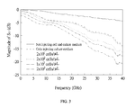
- FIG. 3 is a scattering parameter diagram obtained by measuring a biosensor chip having precise count function of the present invention.
- HepG2 human hepatoma cells
- DMEM fetal bovine serum of 10%
- penicillin 100 unit/ml
- streptomycin 100 ⁇ g/ml
- NaHCO 3 0.3%
- non-essential amino acid 0.1 mM
- sodium pyruvate 1 mM
- the present invention sequentially, injecting the HepG2 cells having different densities (2 ⁇ 10 1 cells/ ⁇ L, 2 ⁇ 10 2 cells/ ⁇ L, 1 ⁇ 10 3 cells/ ⁇ L and 2 ⁇ 10 3 cells/ ⁇ L) and the culture medium into the cell sensing region of the biosensor chip of the present invention, and measuring the scattering parameter S 21 by Agilent N5247 vector network analyzer.
- the present invention further measures the scattering parameter S 21 which is not injected the HepG2 cells and the culture medium, but only injects the culture medium.
- [ S 11 S 12 S 21 S 22 ] loaded is a loaded scattering parameter obtained by measuring the biosensor chip injecting the HepG2 cells and the culture medium;
- medium is a medium scattering parameter obtained by measuring the biosensor chip only injecting the culture medium
- L is a length of the signal waveguide layer and is 6600 ⁇ m in the embodiment; ⁇ eff (f) is an effective dielectric constant; f is a frequency, and c is light velocity of 3 ⁇ 10 8 m/s.
- ⁇ eff ⁇ ( f ) 1 + ⁇ r ⁇ ( f ) - 1 2 ⁇ K ⁇ ( k 1 ) K ⁇ ( k 1 ′ ) ⁇ K ⁇ ( k 0 ′ ) K ⁇ ( k 0 ) ⁇ ( d ) , and can further obtain a characteristic impedance Z 0 (f) by the effective dielectric constant
- ⁇ eff ⁇ ( f ) , Z 0 ⁇ ( f ) 30 ⁇ ⁇ ⁇ eff ⁇ ( f ) ⁇ K ⁇ ( k 0 ′ ) K ⁇ ( k 0 ) ⁇ ( ⁇ ) ⁇ ( e ) , and wherein ⁇ r (f) is an dielectric constant; K(x) is an elliptical integral of a first kind;
- FIGS. 4 a and 4 b are a cell-based attenuation constant diagram obtained by a method of sensing cell of the present invention and a cell-based dielectric constant diagram obtained by a method of sensing cell of the present invention, respectively.
- the scattering parameter of the relation (a) has deleted the microwave parasitic effect of the culture medium and the substrate, it can obtain pure dielectric property of the HepG2 cells.
- FIG. 4 a shows, when frequency is 40 GHz, the attenuation constant ⁇ (f) of the HepG2 cells having density of 2 ⁇ 10 1 cells/ ⁇ L, 2 ⁇ 10 2 cells/ ⁇ L, 1 ⁇ 10 3 cells/ ⁇ L and 2 ⁇ 10 3 cells/ ⁇ L are 0.12 ⁇ 10 ⁇ 3 dB/ ⁇ m, 0.58 ⁇ 10 ⁇ 3 dB/ ⁇ m, 0.81 ⁇ 10 ⁇ 3 dB/ ⁇ m and 1.26 ⁇ 10 ⁇ 3 dB/ ⁇ m, respectively. And as shown in FIG.
- FIGS. 5, 6 a and 6 b are an equivalent circuit diagram of a preferred embodiment of a method of sensing cell of the present invention, a cell equivalent resistance diagram obtained by a method of sensing cell of the present invention and a cell equivalent capacitance diagram obtained by a method of sensing cell of the present invention, respectively.
- ⁇ Y 2 ⁇ 1 R ⁇ ( f ) + j ⁇ ⁇ ⁇ ⁇ L ⁇ ( f ) ⁇
- cell ⁇ ( 1 - ⁇ 2 ⁇ L ⁇ ( f ) ⁇ C ⁇ ( f ) cell ) + j ⁇ ( ⁇ ⁇ R ⁇ ( f ) cell ⁇ C ⁇ ( f ) cell + ⁇ ⁇ R ⁇ ( f ) ⁇ C ⁇ ( f ) cell ) ( R ⁇ ( f ) ) ( R
- the electrical characteristic of the HepG2 cells can be explicitly explained via the relations (l), (m) and (n).
- the equivalent resistance R(f) cell of the HepG2 cells will increase from 8.7 ⁇ to 177.9 ⁇
- the equivalent capacitance C(f) cell of the HepG2 cells will increase from 2.53 pF to 2.88 pF.
- the biosensor chip and method of sensing cell of the present invention it can thereby effectively enhance the sensitivity while measuring the HepG2 cells and to obtain amount of the HepG2 cells more precisely so as to prevent carcinogenesis effectively.
Landscapes
- Physics & Mathematics (AREA)
- Life Sciences & Earth Sciences (AREA)
- Health & Medical Sciences (AREA)
- Engineering & Computer Science (AREA)
- Chemical & Material Sciences (AREA)
- Bioinformatics & Cheminformatics (AREA)
- General Health & Medical Sciences (AREA)
- Spectroscopy & Molecular Physics (AREA)
- Biotechnology (AREA)
- Biophysics (AREA)
- Bioinformatics & Computational Biology (AREA)
- Medical Informatics (AREA)
- Evolutionary Biology (AREA)
- Theoretical Computer Science (AREA)
- Analytical Chemistry (AREA)
- Molecular Biology (AREA)
- Immunology (AREA)
- Biochemistry (AREA)
- General Physics & Mathematics (AREA)
- Pathology (AREA)
- Proteomics, Peptides & Aminoacids (AREA)
- Genetics & Genomics (AREA)
- Electromagnetism (AREA)
- Physiology (AREA)
- Crystallography & Structural Chemistry (AREA)
- Electrochemistry (AREA)
- Chemical Kinetics & Catalysis (AREA)
- Apparatus Associated With Microorganisms And Enzymes (AREA)
- Organic Chemistry (AREA)
- Investigating Or Analyzing Materials By The Use Of Electric Means (AREA)
- Wood Science & Technology (AREA)
- Zoology (AREA)
- Toxicology (AREA)
- Microbiology (AREA)
- General Engineering & Computer Science (AREA)
Abstract
Description
and amount of the cells is obtained from the cell scattering parameter
is a loaded scattering parameter obtained by measuring the biosensor chip injecting the cell and the culture medium;
is a medium scattering parameter obtained by measuring the biosensor chip only injecting the culture medium; and
is an unloaded scattering parameter obtained by measuring the biosensor chip not injecting the cell and the culture medium.
and wherein L is a length of the signal waveguide layer; ∈eff(f) is an effective dielectric constant; f is a frequency.
from the effective dielectric constant ∈eff(f), and wherein K(x) is an elliptical integral of a first kind;
s is a width of the signal waveguide layer; G is an interval between the ground wire waveguide layer and the signal waveguide layer; and h is a thickness of the substrate.
and wherein,
is a loaded scattering parameter obtained by measuring the biosensor chip injecting the HepG2 cells and the culture medium;
is a medium scattering parameter obtained by measuring the biosensor chip only injecting the culture medium; and
is an unloaded scattering parameter obtained by measuring the biosensor chip not injecting the HepG2 cells and the culture medium.
Wherein, L is a length of the signal waveguide layer and is 6600 μm in the embodiment; ∈eff(f) is an effective dielectric constant; f is a frequency, and c is light velocity of 3×10⁸ m/s.
and can further obtain a characteristic impedance Z0(f) by the effective dielectric constant
and wherein ∈r(f) is an dielectric constant; K(x) is an elliptical integral of a first kind;
s is a width of the signal waveguide layer; G is an interval between the ground wire waveguide layer and the signal waveguide layer; and h is a thickness of the substrate.
γ(f)×Z 0(f)=R(f)+jω·L(f) (f), and
γ(f)/Z 0(f)=G(f)+jω·C(f) (g)
to obtain an equivalent resistance R(f)cell and an equivalent capacitance C(f)cell of the HepG2 cells, wherein R(f) is a resistance, L(f) is an inductance, G(f) is an conductance, C(f) is a capacitance and ω is an angular frequency.
in form of
wherein, Y1 is an equivalent circuit of the substrate, and Y2 is an equivalent circuit of the culture medium and the HepG2 cells.
Claims (6)
Applications Claiming Priority (3)
| Application Number | Priority Date | Filing Date | Title |
|---|---|---|---|
| TW103110187A TWI512285B (en) | 2014-03-18 | 2014-03-18 | A method for measuring the number of cells and measuring the number of cells with a precision counting function |
| TW103110187 | 2014-03-18 | ||
| TW103110187A | 2014-03-18 |
Publications (2)
| Publication Number | Publication Date |
|---|---|
| US20150267239A1 US20150267239A1 (en) | 2015-09-24 |
| US9528954B2 true US9528954B2 (en) | 2016-12-27 |
Family
ID=54141523
Family Applications (1)
| Application Number | Title | Priority Date | Filing Date |
|---|---|---|---|
| US14/458,978 Expired - Fee Related US9528954B2 (en) | 2014-03-18 | 2014-08-13 | Biosensor chip having precise count function and method of sensing amount of cells |
Country Status (2)
| Country | Link |
|---|---|
| US (1) | US9528954B2 (en) |
| TW (1) | TWI512285B (en) |
Families Citing this family (1)
| Publication number | Priority date | Publication date | Assignee | Title |
|---|---|---|---|---|
| CN107338192B (en) * | 2017-07-18 | 2023-09-08 | 电子科技大学 | A real-time radio frequency acquisition system for biological cell culture |
Citations (1)
| Publication number | Priority date | Publication date | Assignee | Title |
|---|---|---|---|---|
| US20030039455A1 (en) * | 2001-08-21 | 2003-02-27 | Toshihiko Ouchi | Optical waveguide apparatus |
Family Cites Families (1)
| Publication number | Priority date | Publication date | Assignee | Title |
|---|---|---|---|---|
| GB0117715D0 (en) * | 2001-07-19 | 2001-09-12 | Mrbp Res Ltd | Microwave biochemical analysis |
-
2014
- 2014-03-18 TW TW103110187A patent/TWI512285B/en not_active IP Right Cessation
- 2014-08-13 US US14/458,978 patent/US9528954B2/en not_active Expired - Fee Related
Patent Citations (1)
| Publication number | Priority date | Publication date | Assignee | Title |
|---|---|---|---|---|
| US20030039455A1 (en) * | 2001-08-21 | 2003-02-27 | Toshihiko Ouchi | Optical waveguide apparatus |
Non-Patent Citations (3)
| Title |
|---|
| "Scattering parameters," https://en.wikipedia.org/wiki/Scattering-parameters, Contents 3: Two-Port S-Parameters, first published on Aug. 11, 2013. |
| Yang et al. Characteristics of coplanar waveguide on lithium niobate crystals as a microwave substrate. Journal of Applied Physics, vol. 101, 2007, article 014101, pp. 1-5. * |
| Yang et al. Distinguishing the viability of a single yeast cell with an ultra-sensitive radio frequency sensor. Lab on a Chip, 2010, vol. 10, pp. 553-555. * |
Also Published As
| Publication number | Publication date |
|---|---|
| TWI512285B (en) | 2015-12-11 |
| US20150267239A1 (en) | 2015-09-24 |
| TW201537165A (en) | 2015-10-01 |
Similar Documents
| Publication | Publication Date | Title |
|---|---|---|
| US11662308B2 (en) | Biological sampling and analysis method | |
| EP2929333B1 (en) | A microfabricated sensor and a method of sensing the level of a component in bodily fluid | |
| Yi et al. | Noninvasive glucose sensors using defective-ground-structure coplanar waveguide | |
| US20090236529A1 (en) | Detecting apparatus, and detecting method | |
| KR101892540B1 (en) | Method and apparatus for measuring radio frequency properties of biomaterial | |
| US8962305B2 (en) | Biosensor chip with nanostructures | |
| US20180143145A1 (en) | Sensor for performing dielectric measurements | |
| US10539491B2 (en) | Apparatus and method for measuring erythrocyte sedimentation rate | |
| Dalmay et al. | Label free biosensors for human cell characterization using radio and microwave frequencies | |
| Mansour et al. | A novel approach to non-invasive blood glucose sensing based on a defected ground structure | |
| Chen et al. | Microwave dielectric spectroscopy of a single biological cell with improved sensitivity up to 40 GHz | |
| KR101433268B1 (en) | Apparatus and method for detecting foreign material using terahertz metamaterials | |
| US9528954B2 (en) | Biosensor chip having precise count function and method of sensing amount of cells | |
| KR20160109220A (en) | Biosensor, method for sensing physiological data using a biosensor, and method for manufacturing a biosensor | |
| KR102037251B1 (en) | Method for analyzing cancer cell dna using near-field amplification of metamaterial sensor | |
| CN114527090A (en) | Terahertz biosensor based on combination of coplanar waveguide and resonant structure | |
| Cong et al. | High-sensitivity flexible meta-surface for terahertz-based breast cancer differentiation: Study in cellular and fresh tissue | |
| WO2021124393A1 (en) | Dielectric spectrometry device | |
| Meyne et al. | Corrugated coplanar transmission-line sensor for broadband liquid sample characterization | |
| KR20180124673A (en) | Quantitative Detection method of Glucose Level Based on RF Patch Biosensor Combined with Volume-fixed Structures | |
| Omer et al. | Compact honey-cell CSRR-based microwave newline biosensor for monitoring glucose levels | |
| Omer et al. | Multiple-pole CSRR-based microwave sensor for glucose levels detection | |
| KR20180084327A (en) | Biosensor having RF bandstop filter structure, method for sensing physiological data using an RF biosensor having metal line and sir-bridge structure to sense glusose concentration, and method for manufacturing a biosensor | |
| Hamdani et al. | Design of a microwave biosensor using a defected CSRR for cancer cells characterization | |
| Dalmay et al. | RF biosensor based on microwave filter for biological cell characterisation |
Legal Events
| Date | Code | Title | Description |
|---|---|---|---|
| AS | Assignment |
Owner name: KUN SHAN UNIVERSITY, TAIWAN Free format text: ASSIGNMENT OF ASSIGNORS INTEREST;ASSIGNORS:WU, HUNG-WEI;CHEN, YU-FU;HONG, YONG-HAN;AND OTHERS;SIGNING DATES FROM 20140617 TO 20140619;REEL/FRAME:033550/0014 |
|
| FEPP | Fee payment procedure |
Free format text: PAYOR NUMBER ASSIGNED (ORIGINAL EVENT CODE: ASPN); ENTITY STATUS OF PATENT OWNER: SMALL ENTITY |
|
| STCF | Information on status: patent grant |
Free format text: PATENTED CASE |
|
| MAFP | Maintenance fee payment |
Free format text: PAYMENT OF MAINTENANCE FEE, 4TH YR, SMALL ENTITY (ORIGINAL EVENT CODE: M2551); ENTITY STATUS OF PATENT OWNER: SMALL ENTITY Year of fee payment: 4 |
|
| FEPP | Fee payment procedure |
Free format text: MAINTENANCE FEE REMINDER MAILED (ORIGINAL EVENT CODE: REM.); ENTITY STATUS OF PATENT OWNER: SMALL ENTITY |
|
| LAPS | Lapse for failure to pay maintenance fees |
Free format text: PATENT EXPIRED FOR FAILURE TO PAY MAINTENANCE FEES (ORIGINAL EVENT CODE: EXP.); ENTITY STATUS OF PATENT OWNER: SMALL ENTITY |
|
| STCH | Information on status: patent discontinuation |
Free format text: PATENT EXPIRED DUE TO NONPAYMENT OF MAINTENANCE FEES UNDER 37 CFR 1.362 |
|
| FP | Lapsed due to failure to pay maintenance fee |
Effective date: 20241227 |