US9525027B2 - Lateral bipolar junction transistor having graded SiGe base - Google Patents
Lateral bipolar junction transistor having graded SiGe base Download PDFInfo
- Publication number
- US9525027B2 US9525027B2 US14/208,518 US201414208518A US9525027B2 US 9525027 B2 US9525027 B2 US 9525027B2 US 201414208518 A US201414208518 A US 201414208518A US 9525027 B2 US9525027 B2 US 9525027B2
- Authority
- US
- United States
- Prior art keywords
- region
- germanium
- silicon
- channel region
- dummy gate
- Prior art date
- Legal status (The legal status is an assumption and is not a legal conclusion. Google has not performed a legal analysis and makes no representation as to the accuracy of the status listed.)
- Expired - Fee Related, expires
Links
Images


Classifications
-
- H—ELECTRICITY
- H10—SEMICONDUCTOR DEVICES; ELECTRIC SOLID-STATE DEVICES NOT OTHERWISE PROVIDED FOR
- H10D—INORGANIC ELECTRIC SEMICONDUCTOR DEVICES
- H10D62/00—Semiconductor bodies, or regions thereof, of devices having potential barriers
- H10D62/10—Shapes, relative sizes or dispositions of the regions of the semiconductor bodies; Shapes of the semiconductor bodies
- H10D62/17—Semiconductor regions connected to electrodes not carrying current to be rectified, amplified or switched, e.g. channel regions
- H10D62/177—Base regions of bipolar transistors, e.g. BJTs or IGBTs
- H10D62/184—Base regions of bipolar transistors, e.g. BJTs or IGBTs of lateral BJTs
-
- H01L29/1008—
-
- H01L21/2254—
-
- H01L21/8249—
-
- H01L27/0623—
-
- H01L29/0808—
-
- H01L29/0821—
-
- H01L29/41708—
-
- H01L29/6625—
-
- H01L29/66795—
-
- H01L29/735—
-
- H—ELECTRICITY
- H10—SEMICONDUCTOR DEVICES; ELECTRIC SOLID-STATE DEVICES NOT OTHERWISE PROVIDED FOR
- H10D—INORGANIC ELECTRIC SEMICONDUCTOR DEVICES
- H10D10/00—Bipolar junction transistors [BJT]
- H10D10/01—Manufacture or treatment
- H10D10/061—Manufacture or treatment of lateral BJTs
-
- H—ELECTRICITY
- H10—SEMICONDUCTOR DEVICES; ELECTRIC SOLID-STATE DEVICES NOT OTHERWISE PROVIDED FOR
- H10D—INORGANIC ELECTRIC SEMICONDUCTOR DEVICES
- H10D10/00—Bipolar junction transistors [BJT]
- H10D10/60—Lateral BJTs
-
- H—ELECTRICITY
- H10—SEMICONDUCTOR DEVICES; ELECTRIC SOLID-STATE DEVICES NOT OTHERWISE PROVIDED FOR
- H10D—INORGANIC ELECTRIC SEMICONDUCTOR DEVICES
- H10D30/00—Field-effect transistors [FET]
- H10D30/01—Manufacture or treatment
- H10D30/021—Manufacture or treatment of FETs having insulated gates [IGFET]
- H10D30/024—Manufacture or treatment of FETs having insulated gates [IGFET] of fin field-effect transistors [FinFET]
-
- H—ELECTRICITY
- H10—SEMICONDUCTOR DEVICES; ELECTRIC SOLID-STATE DEVICES NOT OTHERWISE PROVIDED FOR
- H10D—INORGANIC ELECTRIC SEMICONDUCTOR DEVICES
- H10D62/00—Semiconductor bodies, or regions thereof, of devices having potential barriers
- H10D62/10—Shapes, relative sizes or dispositions of the regions of the semiconductor bodies; Shapes of the semiconductor bodies
- H10D62/13—Semiconductor regions connected to electrodes carrying current to be rectified, amplified or switched, e.g. source or drain regions
- H10D62/133—Emitter regions of BJTs
- H10D62/134—Emitter regions of BJTs of lateral BJTs
-
- H—ELECTRICITY
- H10—SEMICONDUCTOR DEVICES; ELECTRIC SOLID-STATE DEVICES NOT OTHERWISE PROVIDED FOR
- H10D—INORGANIC ELECTRIC SEMICONDUCTOR DEVICES
- H10D62/00—Semiconductor bodies, or regions thereof, of devices having potential barriers
- H10D62/10—Shapes, relative sizes or dispositions of the regions of the semiconductor bodies; Shapes of the semiconductor bodies
- H10D62/13—Semiconductor regions connected to electrodes carrying current to be rectified, amplified or switched, e.g. source or drain regions
- H10D62/137—Collector regions of BJTs
-
- H—ELECTRICITY
- H10—SEMICONDUCTOR DEVICES; ELECTRIC SOLID-STATE DEVICES NOT OTHERWISE PROVIDED FOR
- H10D—INORGANIC ELECTRIC SEMICONDUCTOR DEVICES
- H10D64/00—Electrodes of devices having potential barriers
- H10D64/20—Electrodes characterised by their shapes, relative sizes or dispositions
- H10D64/23—Electrodes carrying the current to be rectified, amplified, oscillated or switched, e.g. sources, drains, anodes or cathodes
- H10D64/231—Emitter or collector electrodes for bipolar transistors
-
- H—ELECTRICITY
- H10—SEMICONDUCTOR DEVICES; ELECTRIC SOLID-STATE DEVICES NOT OTHERWISE PROVIDED FOR
- H10D—INORGANIC ELECTRIC SEMICONDUCTOR DEVICES
- H10D84/00—Integrated devices formed in or on semiconductor substrates that comprise only semiconducting layers, e.g. on Si wafers or on GaAs-on-Si wafers
- H10D84/01—Manufacture or treatment
- H10D84/0107—Integrating at least one component covered by H10D12/00 or H10D30/00 with at least one component covered by H10D8/00, H10D10/00 or H10D18/00, e.g. integrating IGFETs with BJTs
- H10D84/0109—Integrating at least one component covered by H10D12/00 or H10D30/00 with at least one component covered by H10D8/00, H10D10/00 or H10D18/00, e.g. integrating IGFETs with BJTs the at least one component covered by H10D12/00 or H10D30/00 being a MOS device
-
- H—ELECTRICITY
- H10—SEMICONDUCTOR DEVICES; ELECTRIC SOLID-STATE DEVICES NOT OTHERWISE PROVIDED FOR
- H10D—INORGANIC ELECTRIC SEMICONDUCTOR DEVICES
- H10D84/00—Integrated devices formed in or on semiconductor substrates that comprise only semiconducting layers, e.g. on Si wafers or on GaAs-on-Si wafers
- H10D84/01—Manufacture or treatment
- H10D84/02—Manufacture or treatment characterised by using material-based technologies
- H10D84/03—Manufacture or treatment characterised by using material-based technologies using Group IV technology, e.g. silicon technology or silicon-carbide [SiC] technology
- H10D84/038—Manufacture or treatment characterised by using material-based technologies using Group IV technology, e.g. silicon technology or silicon-carbide [SiC] technology using silicon technology, e.g. SiGe
-
- H—ELECTRICITY
- H10—SEMICONDUCTOR DEVICES; ELECTRIC SOLID-STATE DEVICES NOT OTHERWISE PROVIDED FOR
- H10D—INORGANIC ELECTRIC SEMICONDUCTOR DEVICES
- H10D84/00—Integrated devices formed in or on semiconductor substrates that comprise only semiconducting layers, e.g. on Si wafers or on GaAs-on-Si wafers
- H10D84/40—Integrated devices formed in or on semiconductor substrates that comprise only semiconducting layers, e.g. on Si wafers or on GaAs-on-Si wafers characterised by the integration of at least one component covered by groups H10D12/00 or H10D30/00 with at least one component covered by groups H10D10/00 or H10D18/00, e.g. integration of IGFETs with BJTs
- H10D84/401—Combinations of FETs or IGBTs with BJTs
-
- H—ELECTRICITY
- H10—SEMICONDUCTOR DEVICES; ELECTRIC SOLID-STATE DEVICES NOT OTHERWISE PROVIDED FOR
- H10P—GENERIC PROCESSES OR APPARATUS FOR THE MANUFACTURE OR TREATMENT OF DEVICES COVERED BY CLASS H10
- H10P32/00—Diffusion of dopants within, into or out of wafers, substrates or parts of devices
- H10P32/10—Diffusion of dopants within, into or out of semiconductor bodies or layers
- H10P32/14—Diffusion of dopants within, into or out of semiconductor bodies or layers within a single semiconductor body or layer in a solid phase; between different semiconductor bodies or layers, both in a solid phase
- H10P32/1408—Diffusion of dopants within, into or out of semiconductor bodies or layers within a single semiconductor body or layer in a solid phase; between different semiconductor bodies or layers, both in a solid phase from or through or into an external applied layer, e.g. photoresist or nitride layers
-
- H—ELECTRICITY
- H10—SEMICONDUCTOR DEVICES; ELECTRIC SOLID-STATE DEVICES NOT OTHERWISE PROVIDED FOR
- H10P—GENERIC PROCESSES OR APPARATUS FOR THE MANUFACTURE OR TREATMENT OF DEVICES COVERED BY CLASS H10
- H10P32/00—Diffusion of dopants within, into or out of wafers, substrates or parts of devices
- H10P32/10—Diffusion of dopants within, into or out of semiconductor bodies or layers
- H10P32/17—Diffusion of dopants within, into or out of semiconductor bodies or layers characterised by the semiconductor material
- H10P32/171—Diffusion of dopants within, into or out of semiconductor bodies or layers characterised by the semiconductor material being group IV material
-
- H01L27/0924—
-
- H01L29/0692—
-
- H01L29/4232—
-
- H—ELECTRICITY
- H10—SEMICONDUCTOR DEVICES; ELECTRIC SOLID-STATE DEVICES NOT OTHERWISE PROVIDED FOR
- H10D—INORGANIC ELECTRIC SEMICONDUCTOR DEVICES
- H10D30/00—Field-effect transistors [FET]
- H10D30/60—Insulated-gate field-effect transistors [IGFET]
- H10D30/62—Fin field-effect transistors [FinFET]
-
- H—ELECTRICITY
- H10—SEMICONDUCTOR DEVICES; ELECTRIC SOLID-STATE DEVICES NOT OTHERWISE PROVIDED FOR
- H10D—INORGANIC ELECTRIC SEMICONDUCTOR DEVICES
- H10D62/00—Semiconductor bodies, or regions thereof, of devices having potential barriers
- H10D62/10—Shapes, relative sizes or dispositions of the regions of the semiconductor bodies; Shapes of the semiconductor bodies
- H10D62/124—Shapes, relative sizes or dispositions of the regions of semiconductor bodies or of junctions between the regions
- H10D62/126—Top-view geometrical layouts of the regions or the junctions
-
- H—ELECTRICITY
- H10—SEMICONDUCTOR DEVICES; ELECTRIC SOLID-STATE DEVICES NOT OTHERWISE PROVIDED FOR
- H10D—INORGANIC ELECTRIC SEMICONDUCTOR DEVICES
- H10D64/00—Electrodes of devices having potential barriers
- H10D64/20—Electrodes characterised by their shapes, relative sizes or dispositions
- H10D64/27—Electrodes not carrying the current to be rectified, amplified, oscillated or switched, e.g. gates
- H10D64/311—Gate electrodes for field-effect devices
- H10D64/411—Gate electrodes for field-effect devices for FETs
- H10D64/511—Gate electrodes for field-effect devices for FETs for IGFETs
-
- H—ELECTRICITY
- H10—SEMICONDUCTOR DEVICES; ELECTRIC SOLID-STATE DEVICES NOT OTHERWISE PROVIDED FOR
- H10D—INORGANIC ELECTRIC SEMICONDUCTOR DEVICES
- H10D84/00—Integrated devices formed in or on semiconductor substrates that comprise only semiconducting layers, e.g. on Si wafers or on GaAs-on-Si wafers
- H10D84/80—Integrated devices formed in or on semiconductor substrates that comprise only semiconducting layers, e.g. on Si wafers or on GaAs-on-Si wafers characterised by the integration of at least one component covered by groups H10D12/00 or H10D30/00, e.g. integration of IGFETs
- H10D84/82—Integrated devices formed in or on semiconductor substrates that comprise only semiconducting layers, e.g. on Si wafers or on GaAs-on-Si wafers characterised by the integration of at least one component covered by groups H10D12/00 or H10D30/00, e.g. integration of IGFETs of only field-effect components
- H10D84/83—Integrated devices formed in or on semiconductor substrates that comprise only semiconducting layers, e.g. on Si wafers or on GaAs-on-Si wafers characterised by the integration of at least one component covered by groups H10D12/00 or H10D30/00, e.g. integration of IGFETs of only field-effect components of only insulated-gate FETs [IGFET]
- H10D84/85—Complementary IGFETs, e.g. CMOS
- H10D84/853—Complementary IGFETs, e.g. CMOS comprising FinFETs
Definitions
- the present disclosure relates to the physical sciences, and, more particularly, to bipolar junction transistors and methods of fabrication thereof.
- Bipolar junction transistors include emitter, collector and base regions. A biasing voltage applied between a base contact and an emitter contact allows control of collector current. Bipolar junction transistors can be employed in applications such as switches or amplifiers. Depending on the doping types associated with the base, emitter and collector regions, bipolar junction transistors may operate as p-n-p transistors or n-p-n transistors. A heterojunction bipolar transistor, which is a type of bipolar junction transistor, operates based on a bandgap difference between the emitter and base. Significant current gains can be obtained through the use of heterojunction bipolar transistors.
- FETs field effect transistors
- the substrates may include semiconductor on insulator (SOI) substrates or bulk semiconductor substrates.
- Silicon fins are formed in some FinFETs on substrates via known technology such as sidewall image transfer (SIT).
- FinFET structures including SOI substrates can be formed, in part, by selectively etching the crystalline silicon layers down to the oxide or other insulating layers thereof following photolithography.
- Active fin heights are set by SOI thickness when employing SOI substrates. In bulk FinFETs, active fin height is set by oxide thickness and etched fin height.
- the gates of FinFETs can be formed using a “gate-first” process wherein a gate stack and spacers are formed prior to selective epitaxial growth wherein source and drain regions are enlarged.
- a “gate-last” process may alternatively be employed wherein the source/drain regions are formed immediately following fin patterning. Gate-last procedures can involve making a dummy gate, fabricating other elements of the transistor, removing the dummy gate, and replacing the removed dummy gate with actual gate materials.
- Principles of the present disclosure provide an exemplary fabrication method that includes obtaining a structure comprising a plurality of parallel silicon fins adjoining an electrically insulating layer and a dummy gate extending across a plurality of the silicon fins.
- the fins define a channel region having a first conductivity type beneath the dummy gate.
- the structure further includes a source region on a first side of the dummy gate and a drain region on a second side of the dummy gate. Germanium is diffused into the channel region of the structure to form a germanium gradient within the channel region. Germanium content within the channel region increases in the direction of the drain region. The drain region is removed.
- a silicon region is epitaxially grown on the second side of the dummy gate.
- the silicon region is grown from the fins within the channel region subsequent to forming the germanium gradient.
- the method further includes doping the silicon region such that the silicon region has a second conductivity type opposite to the first conductivity type, replacing the dummy gate with a gate structure operatively associated with the channel region, and forming electrical connections to the gate structure and the silicon region.
- a lateral bipolar junction transistor in accordance with an exemplary embodiment includes a substrate including an electrically insulating layer, a doped silicon base region adjoining the electrically insulating layer and having a first conductivity type, and a doped silicon emitter region adjoining the electrically insulating layer and the base region, the doped silicon emitter region having a second conductivity type.
- a doped silicon collector region adjoin the electrically insulating layer and the base region and has the second conductivity type.
- a germanium gradient within the doped silicon base region has an increasing germanium content in the direction of the collector region.
- a gate structure is operatively associated with the doped silicon base region.
- facilitating includes performing the action, making the action easier, helping to carry the action out, or causing the action to be performed.
- instructions executing on one processor might facilitate an action carried out by instructions executing on a remote processor, by sending appropriate data or commands to cause or aid the action to be performed.
- the action is nevertheless performed by some entity or combination of entities.
- LJTs Lateral bipolar junction transistors
- fabrication methods as disclosed herein can provide substantial beneficial technical effects.
- one or more embodiments may provide one or more of the following advantages:
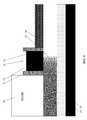
- FIG. 1A is a schematic sectional illustration of a FinFET structure following formation of a dummy gate
- FIG. 1B is a top plan view of the structure shown in FIG. 1A ;
- FIG. 2A is a schematic sectional illustration of the structure shown in FIG. 1A including a mask formed thereon;
- FIG. 2B a top plan view of the structure shown in FIG. 2A ;
- FIG. 3A is a schematic sectional illustration of the structure shown in FIG. 2A showing silicon germanium merge epitaxy in the drain region;
- FIG. 3B a top plan view of the structure shown in FIG. 3A ;
- FIG. 4 is a schematic sectional illustration of the structure shown in FIG. 3 showing annealing of the structure to form a germanium gradient in the channel region;
- FIG. 5 is a schematic sectional illustration showing formation of a recess in the drain region of the structure shown in FIG. 4 ;
- FIG. 6 is a schematic sectional illustration showing formation of a highly doped epitaxial silicon region in the drain region of the structure shown in FIG. 5 ;
- FIG. 7 is a schematic sectional illustration showing removal of the mask from the structure shown in FIG. 6 ;
- FIG. 8 is a schematic sectional illustration showing growth of a silicon region on both the source and drain regions of the structure shown in FIG. 7 ;
- FIG. 9 is a schematic sectional illustration showing formation of a gate structure, source and drain electrodes, and a dielectric layer on the structure shown in FIG. 8 ;
- FIG. 10 is a schematic sectional illustration showing formation of a recess in the drain portion of the structure shown in FIG. 2 ;
- FIG. 11 is a schematic sectional illustration showing formation of a germanium layer in the drain portion of the structure shown in FIG. 11 ;
- FIG. 12 is a schematic sectional illustration of the structure shown in FIG. 11 showing annealing of the structure to form a germanium gradient in the channel region, and
- FIG. 13 is a schematic sectional illustration showing the structure of FIG. 12 following removal of the germanium layer from the drain region.
- Lateral bipolar junction transistors having graded germanium content in the base portions thereof are provided, thereby boosting current gain.
- the bipolar junction transistors are formed in some embodiments using, in part, technology that is also employed for forming FinFET structures.
- FinFET structures are characterized by fins formed on semiconductor substrates. Such substrates include bulk silicon substrates (fin on bulk) and SOI substrates (fin on SOI) as discussed above.
- substrates include bulk silicon substrates (fin on bulk) and SOI substrates (fin on SOI) as discussed above.
- the processes discussed below relate to fabrication of electronic devices from SOI substrates, though bulk silicon substrates may alternatively be employed.
- FIGS. 1-9 illustrate exemplary steps that may be performed sequentially in fabricating lateral bipolar junction transistors, it being appreciated that additional steps may be necessary depending on the desired features of the structures.
- Fabrication may commence with a partially completed structure, in which case one or more of the steps described below could be omitted.
- Fabrication of the lateral bipolar junction transistors as described below is accompanied in some embodiments by fabrication of CMOS FinFET devices on the same chip.
- a SOI substrate comprised of essentially undoped crystalline silicon is employed for forming a finned structure 20 as shown in FIGS. 1A and 1B , it being appreciated that standard silicon substrates may have a very low level of p-doping.
- the substrate may be in the form of a wafer.
- the finned structure includes an array of parallel silicon fins 22 formed from the SOI layer of the substrate, a substrate layer 24 that functions as a handle, and an electrically insulating layer 26 such as a buried oxide layer.
- the electrically insulating layer 26 in one exemplary embodiment is a high quality silicon dioxide layer that is thermally grown, though other buried insulators such as boron nitride (BN) and aluminum oxide (Al 2 O 3 ) may alternatively be employed in some embodiments.
- High quality buried oxides are generally characterized by relatively low interface trap densities (D it ). Fin heights, widths and spacing are further chosen in accordance with manufacturer preferences. Fin heights in some embodiments range between 10-60 nm. As discussed above, fin heights correspond to the thickness of the SOI layer from which they are formed.
- the side walls of the fins 22 may not be exactly vertical and instead converge towards the tops of the fins.
- Exposed fin surfaces in one or more embodiments may be (110) surfaces or close to (110) surfaces, but may or may not be exactly (110) surfaces.
- a sacrificial “dummy” gate 28 is formed on a portion of the finned structure 20 and extends perpendicularly to the fins 22 .
- the sacrificial gate is a structure that defines the geometry of a later formed gate structure that operates the semiconductor device once the dummy gate is removed and the gate structure that operates the semiconductor device is formed in its place, as described further below.
- the dummy gate is removed in a later process familiar to those of skill in the art and a replacement metal gate composition is patterned at an appropriate stage of the transistor fabrication process.
- the sacrificial dummy gate 28 is comprised of a sacrificial gate oxide 30 on the SOI layer that includes the fins 22 and a dielectric cap 32 on top of the polysilicon layer.
- the disclosed sacrificial gate materials are considered exemplary as opposed to limiting. Other suitable material or combinations of materials familiar to those of skill in the art may alternatively be employed.
- Spacers 34 are formed on the sidewalls of the gate. The spacers are formed by depositing a dielectric material different from the material used for the cap 32 in one or more embodiments to allow for subsequent selective etching of the cap 32 and spacers 34 .
- the spacers 34 can include silicon oxide.
- the dielectric spacers 34 are formed in some embodiments by depositing a layer of dielectric material on the structure and anisotropically etching the layer.
- the dummy gate 28 is formed on the channel region of the silicon fins.
- the region adjoining a first side of the channel region is referred herein to as a source region while the region adjoining the opposite side of the channel region is referred to as a drain region, it being appreciated that at least the drain region is removed during fabrication and replaced by an epitaxial region that functions as the drain (collector) region of the lateral bipolar junction transistor obtained.
- a mask 36 is formed over the source region of the lateral bipolar junction transistor to be formed using the SOI substrate.
- the source region thereof is accordingly protected while the drain region is exposed.
- the mask may also extend in part over the dummy gate 32 , though such extension is not required.
- a nitride (silicon nitride (Si 3 N 4 )) hard mask is employed in one or more embodiments.
- Such a mask may be deposited using conventional deposition techniques such as spin-on coating, CVD, plasma-assisted CVD, or other known techniques.
- Hot phosphoric acid is an exemplary etchant that may be employed to remove selected portions of the mask 36 .
- a germanium-containing layer 40 preferably silicon germanium, is grown epitaxially, for example by chemical vapor deposition (CVD), on the fins 22 in the drain region.
- the germanium-containing layer comprises 20-99% germanium, though more preferably 20-80% germanium. In other embodiments, the layer contains 30-60% germanium.
- the thickness of the germanium-containing layer in one or more embodiments is between five to twenty-five nanometers (5-25 nm). As will be appreciated from the discussion below, the germanium-containing layer should have sufficient thickness and sufficient germanium content that the channel (base) region of the lateral bipolar junction transistor to be fabricated contains an acceptable ratio of silicon and germanium.
- the structure obtained following growth of the germanium-containing layer 40 shown in FIGS. 3A and 3B is annealed, resulting in the structure shown in FIG. 4 .
- the anneal process can be furnace anneal, rapid thermal anneal, flash anneal, or any suitable combination of those processes.
- the anneal temperature ranges from 600 degrees to 1300 degrees Centigrade.
- the anneal time ranges from 1 millisecond to 2 hours, depending on the anneal temperature. Higher anneal temperatures require shorter anneal times.
- a typical thermal anneal condition is about thirty minutes at 1000° C. Such annealing causes the mixing of the germanium containing layer 40 and the layer of crystalline silicon fins 22 in the drain and channel regions of the structure.
- a region 42 including a germanium gradient is formed in the channel region beneath the dummy gate, there being an increasing germanium content in the direction of the drain region.
- the region 42 extends all the way to the fin region on the opposite side of the dummy gate 28 that later functions as the source (emitter) region of a finished device.
- the fins 22 in the source region remain germanium-free in one or more embodiments.
- the germanium content of the silicon germanium layer 40 can be engineered as desired for particular applications by depositing a germanium containing layer 24 having an appropriate germanium content and/or thickness for the particular applications.
- the germanium gradient 42 in the channel (base) region is linear in one or more embodiments.
- a recess 41 is formed in the drain region of the structure obtained following thermal annealing.
- the germanium-containing layer 40 , the portions of the silicon fins 22 in the drain region, and a portion of the electrically insulating layer 26 are all removed to form the recess.
- the channel region, including the region 42 thereof containing the germanium gradient, the dummy gate, and the mask 36 remain following formation of the recess.
- Reactive ion etch (RIE) is employed to form the recess 41 in one or more embodiments.
- the anisotropic etch is discontinued within the electrically insulating layer using techniques familiar to those of skill in the art, such as by detecting the presence of the electrically insulating material and/or employing a timed etch that stops before the entirety of the electrically insulating layer is removed. A portion of the electrically insulating layer 26 remains on the substrate following formation of the recess.
- a doped epitaxial silicon region 44 is grown on the exposed surfaces of the fins 22 located beneath the dummy gate, as shown in FIG. 6 .
- Fin thickness is between 5 and 50 nm in one or more embodiments.
- Fin pitch is between 20 and 100 nm and fin height is between 10 and 50 nm in one ore more embodiments. So long as there is some volume of the silicon fins exposed to the epitaxy, by tuning the epitaxy conditions such as temperature, pressure, flow, and time, a merged epitaxial region 44 can be formed for later use as a drain (collector) region. Epitaxy from fins 22 opposite to the illustrated fin may further provide seed material to effect merge of the epitaxial region 44 .
- the epitaxial region 44 By tuning epitaxy conditions such as temperature, pressure, flow, and time, as known to those of skill in the art, it is further possible to grow the epitaxial region 44 selectively to the mask and exposed buried oxide on the field. The process ensures that epitaxy is only nucleated from the exposed SiGe fin regions, not other materials.
- Boron-doped silicon can be formed in one or more exemplary embodiments.
- Phosphorus-doped silicon (Si:P) is formed some exemplary embodiments. The doping level and type can be chosen as desired for particular transistor applications.
- n-type semiconductor regions are formed where the electrons are to function as the majority carriers while holes are the minority carriers.
- P-type semiconductor regions are formed in embodiments wherein the majority carriers are to be holes.
- Boron doping (for example, doping level greater than 1e18) may be provided to form a p+ region.
- the dopant concentration is in the range of 1e19 to 2e20 cm ⁇ 3 .
- the silicon region 44 directly contacts the region 42 containing the diffused germanium.
- doping of the silicon region 44 is in situ during selective epitaxial deposition. Such doping can be effected by flowing a dopant gas including dopant atoms that will provide the appropriate conductivity type in the drain (collector) region of the lateral bipolar junction transistor to be fabricated.
- Silicon-containing reactant gases include but are not limited to SiH 4 , SiH 2 Cl 2 , SiCl 4 and Si 2 H 6 .
- n-type silicon region 44 If an n-type silicon region 44 is to be formed, possible dopant gases include PH 3 , AsH 3 , SbH 3 and combinations thereof.
- One exemplary dopant gas for forming p-type silicon regions is B 3 H 6 .
- the selective epitaxial growth of the silicon region 44 is at a temperature exceeding 500° C.
- doping may be effected by implanting dopants to obtain the desired conductivity type and doping level.
- the source region may be simultaneously doped with the silicon region 44 while protecting the channel region and dummy gate with a hard mask.
- the source (emitter) and drain (collector) regions of the transistor to be fabricated will have the same conductivity type.
- the channel (base) region has a conductivity type opposite from that of the source and drain regions. Heterojunctions are accordingly formed at the interfaces between the emitter and base regions and between the base and collector regions of the subsequently formed lateral bipolar junction transistor.
- Dopants can alternatively be implanted within the source and/or channel regions prior to formation of the dummy gate using hard masks to protect selected areas of the structure while leaving others exposed.
- lithographic techniques can be employed using a soft mask (photoresist) and implanting each desired region separately.
- a further approach for providing dopants includes first, after the diffusion of germanium, using ion implantation while the base (channel) region is protected by the dummy gate, thereby implanting both source and drain regions to achieve source target doping. Since the collector (drain) region is etched later, this ensures the correct source doping level is obtained.
- Collector doping is determined later by silicon epitaxy or masked implantation.
- Dummy dielectric is then deposited as a blanket and subjected to chemical mechanical polishing (CMP) that stops on the dummy gate.
- CMP chemical mechanical polishing
- the dummy gate is then removed and the base (channel) region is implanted while the source and drain regions are protected by the dummy dielectric layer.
- doping thereof is optional.
- a further possible alternative would involve removing fin material from both the source and drain regions rather than just the drain region, leaving the channel in place. Doped source and drain regions would be epitaxially grown on the exposed channel surfaces on both sides of the channel.
- the Kirk effect is a phenomenon associated with bipolar junction transistors and can cause an increase in the base transit time thereof. Increased base transit time reduces current gain ( ⁇ ) and transit frequency at high collector currents.
- the starting substrate is a partially depleted semiconductor-on-insulator (PDSOI) substrate having an SOI layer thickness of about fifty nanometers (50 nm)
- PDSOI semiconductor-on-insulator
- a collector doping density e.g. n-type
- base doping should be higher than collector doping and emitter doping should be higher than base doping.
- base doping level that is less than the collector doping level.
- a value of ⁇ of about ten (10) should be sufficient for one or more applications.
- base doping is about 1e19 cm ⁇ 3
- both emitter and collector doping is greater than 1e20 cm ⁇ 3 and the transistor is symmetrical. Symmetrical lateral bipolar junction transistors provide equal speed in forward-active and reverse-active modes.
- the hard mask 36 is removed from the structure using hot phosphoric acid if the hard mask is a nitride mask.
- Other suitable mask removal techniques may be employed depending on the composition of the mask.
- a silicon layer 46 is grown epitaxially on the fins 22 as shown in FIG. 8 .
- the epitaxial silicon layer 46 grows on both the source region, which is unmerged at the time the silicon layer 46 is deposited, and the drain region, which is a merged structure that adjoins a plurality of the fins 22 . Merging in the source region is optional.
- An object of this step is to provide enough dopant to improve contact resistivity.
- the high doping level of the electrically conductive silicon layer 46 (n+, and a doping level of 1 ⁇ 10 20 cm ⁇ 3 or more in exemplary embodiments) is sufficient to improve contact resistivity. Dopants are provided in situ during deposition of the silicon layer 46 in one or more embodiments.
- the dummy gate is removed in a process familiar to those of skill in the art and a replacement base material 50 is patterned at an appropriate stage of the transistor fabrication process to form a gate structure operatively associated with the base (channel) region 22 B.
- Emitter, base and collector electrodes 52 , 54 , 56 are formed.
- the base and collector electrodes directly contact the highly doped silicon layer 46 .
- the base electrode is formed on the base material 50 .
- Doped poly-Si having a doping density of 1 ⁇ 10 20 cm ⁇ 3 or more is employed as the base material 50 in one or more embodiments.
- BEOL back-end-of-line
- a dielectric layer 58 containing metal layer(s) (not shown) and via conductors 60 .
- Oxide, nitride, and oxynitride materials are among the materials that may comprise the dielectric layer 58 .
- Metallization processes using, for example, copper or aluminum to form the via conductors and metal layer(s), are well known to the art.
- transistors such as the exemplary transistor 62 is scalable and can be fabricated using standard CMOS processing techniques. Such fabrication can be integrated with current FinFET CMOS process flow to provide CMOS FinFET devices (not shown) and LBJT devices on the same chip.
- Steps performed in an alternative exemplary fabrication process are schematically illustrated in FIGS. 10-13 .
- the same reference numerals are employed as found in one or more of FIGS. 1-9 to designate similar elements.
- the alternative process includes obtaining a structure as described above with respect to FIG. 2 . Once such a structure is obtained, a recess 102 is formed in the drain region to provide a structure 100 as shown in FIG. 10 .
- the recess 102 extends into the electrically insulating layer and adjoins the channel region beneath the dummy gate.
- Reactive ion etching is employed in some embodiments to remove the silicon fins in the drain region and a portion of the underlying electrically insulating layer.
- one step RIE is employed in some embodiments to remove both the silicon and insulating (e.g. oxide) layers.
- silicon RIE is followed by oxide RIE in a two-step anisotropic process.
- a merge epitaxy region 104 of substantially pure germanium is grown selectively in the drain region of the structure 100 in some embodiments.
- germanium-containing material such as silicon germanium may comprise the epitaxial region 104 .
- the germanium content of a silicon germanium epitaxial region may be in the range discussed above with respect to the first exemplary method.
- the germanium-containing epitaxial region 104 is formed on the exposed ends of the fins 22 beneath the dummy gate. As schematically illustrated, the region 104 extends laterally from the channel region as well as above and below the planes defined by the top and bottom surfaces of the channel region, similar to the silicon region 44 grown on the fins as shown in FIG. 6 .
- the structure obtained following growth of the germanium region is thermally annealed, causing diffusion of germanium into the portions of the fins comprising the channel region.
- a germanium gradient 106 as shown in FIG. 12 is thereby formed within the silicon channel region.
- the germanium content increases in the direction of the drain region.
- the gradient is linear in some embodiments.
- an etching process is employed to remove the epitaxial germanium region 104 .
- a recess 108 is accordingly formed that exposes the end of the channel region including the germanium gradient 106 .
- the structure obtained is substantially the same as that described above with respect to FIG. 5 . End portions of the fins comprising the channel region are exposed, thereby allowing the growth of a highly doped epitaxial silicon region within the recess 108 that functions as the operational drain region of the LBJT.
- the same steps described above with respect to FIGS. 6-9 are then performed to provide a finished lateral bipolar junction transistor such as shown in FIG. 9 .
- an exemplary fabrication method includes obtaining a structure 20 comprising a plurality of parallel silicon fins 22 adjoining an electrically insulating layer 26 and a dummy gate 28 extending across a plurality of the silicon fins, the fins defining a channel region having a first conductivity type beneath the dummy gate, a source region on a first side of the dummy gate, and a drain region on a second side of the dummy gate.
- the method further includes diffusing germanium into the channel region of the structure to form a germanium gradient 42 ( 106 ) within the channel region of increasing germanium content in the direction of the drain region.
- the drain region defined by the silicon fins 22 of the structure 20 is removed either prior to germanium diffusion, as shown in FIG. 10 , or subsequent to germanium diffusion as shown in FIG. 5 .
- the method further includes epitaxially growing a silicon region 44 on the second (drain) side of the dummy gate and from the fins 22 within the channel region subsequent to forming the germanium gradient 42 ( 106 ).
- the silicon region 44 is doped such that the silicon region has a second conductivity type opposite to the first conductivity type of the channel region.
- the dummy gate 28 is replaced by a functional gate structure that is operatively associated with the channel region 22 B and electrical connections are formed to the gate structure and the silicon region 44 .
- a germanium-containing layer 40 is grown on the drain region and the structure 20 is thermally annealed, thereby causing diffusion of germanium into the channel region as shown in FIG. 4 .
- the germanium is diffused substantially entirely or entirely across the channel region.
- a germanium-containing region is grown on the channel region subsequent to the step of removing the drain region as shown in FIG. 11 . The structure is then thermally annealed, thereby causing diffusion of germanium into the channel region as shown in FIG. 12 .
- germanium has a smaller bandgap than silicon, increasing the germanium content between the emitter and collector regions creates a conduction band gradient that accelerates the transport of electrons (collector current) and retards hole (base) current conduction, thereby boosting current gain in lateral bipolar junction transistors.
- the transistor includes a substrate including an electrically insulating layer 26 .
- a doped silicon base region 22 B adjoins the electrically insulating layer 26 and has a first conductivity type.
- a doped silicon emitter region 22 A adjoins the electrically insulating layer and the base region 22 B, the doped silicon emitter region having a second conductivity type.
- a doped silicon collector region 44 adjoins the electrically insulating layer and the base region, the doped silicon collector region having the second conductivity type.
- a germanium gradient is contained within the doped silicon base region. The germanium content increases in the direction of the collector region.
- a gate structure operatively associated with the doped silicon base region.
- the doped silicon base region includes a plurality of parallel fins.
Landscapes
- Bipolar Transistors (AREA)
Abstract
Description
-
- High drive current per device width;
- High current per layout area;
- Current gain comparable to vertical bipolar junction transistors without polysilicon emitters;
- High frequency operation feasible;
- Integratable with FinFET CMOS process flow.
Claims (14)
Priority Applications (1)
| Application Number | Priority Date | Filing Date | Title |
|---|---|---|---|
| US14/208,518 US9525027B2 (en) | 2014-03-13 | 2014-03-13 | Lateral bipolar junction transistor having graded SiGe base |
Applications Claiming Priority (1)
| Application Number | Priority Date | Filing Date | Title |
|---|---|---|---|
| US14/208,518 US9525027B2 (en) | 2014-03-13 | 2014-03-13 | Lateral bipolar junction transistor having graded SiGe base |
Publications (2)
| Publication Number | Publication Date |
|---|---|
| US20150263091A1 US20150263091A1 (en) | 2015-09-17 |
| US9525027B2 true US9525027B2 (en) | 2016-12-20 |
Family
ID=54069802
Family Applications (1)
| Application Number | Title | Priority Date | Filing Date |
|---|---|---|---|
| US14/208,518 Expired - Fee Related US9525027B2 (en) | 2014-03-13 | 2014-03-13 | Lateral bipolar junction transistor having graded SiGe base |
Country Status (1)
| Country | Link |
|---|---|
| US (1) | US9525027B2 (en) |
Cited By (11)
| Publication number | Priority date | Publication date | Assignee | Title |
|---|---|---|---|---|
| US20170040219A1 (en) * | 2014-04-04 | 2017-02-09 | International Business Machines Corporation | III-V, SiGe, or Ge Base Lateral Bipolar Transistor and CMOS Hybrid Technology |
| US10037989B1 (en) * | 2017-10-26 | 2018-07-31 | International Business Machines Corporation | III-V lateral bipolar integration with silicon |
| US10236346B1 (en) | 2017-10-25 | 2019-03-19 | International Business Machines Corporation | Transistor having a high germanium percentage fin channel and a gradient source/drain junction doping profile |
| US10707336B1 (en) | 2019-02-26 | 2020-07-07 | International Business Machines Corporation | High-performance lateral BJT with epitaxial lightly doped intrinsic base |
| US10734490B1 (en) | 2019-03-22 | 2020-08-04 | International Business Machines Corporation | Bipolar junction transistor (BJT) with 3D wrap around emitter |
| US11094805B2 (en) | 2020-01-17 | 2021-08-17 | Globalfoundries U.S. Inc. | Lateral heterojunction bipolar transistors with asymmetric junctions |
| US11127843B2 (en) | 2019-09-23 | 2021-09-21 | Globalfoundries U.S. Inc. | Asymmetrical lateral heterojunction bipolar transistors |
| US11282947B1 (en) | 2020-09-02 | 2022-03-22 | International Business Machines Corporation | Heterojunction bipolar transistor with a silicon oxide layer on a silicon germanium base |
| US20230155011A1 (en) * | 2021-11-18 | 2023-05-18 | Globalfoundries U.S. Inc. | Lateral bipolar transistor with emitter and collector regions including portions within in-insulator layer cavities and method |
| US11682718B2 (en) | 2021-04-15 | 2023-06-20 | International Business Machines Corporation | Vertical bipolar junction transistor with all-around extrinsic base and epitaxially graded intrinsic base |
| US11916136B2 (en) | 2022-02-25 | 2024-02-27 | Globalfoundries U.S. Inc. | Lateral bipolar junction transistors including a graded silicon-germanium intrinsic base |
Families Citing this family (11)
| Publication number | Priority date | Publication date | Assignee | Title |
|---|---|---|---|---|
| JP2016063021A (en) * | 2014-09-17 | 2016-04-25 | 株式会社東芝 | Resistance change memory, method for manufacturing the same, and fet |
| US9673307B1 (en) * | 2016-04-13 | 2017-06-06 | International Business Machines Corporation | Lateral bipolar junction transistor with abrupt junction and compound buried oxide |
| US9947778B2 (en) | 2016-07-15 | 2018-04-17 | International Business Machines Corporation | Lateral bipolar junction transistor with controlled junction |
| US10170584B2 (en) * | 2017-01-27 | 2019-01-01 | International Business Machines Corporation | Nanosheet field effect transistors with partial inside spacers |
| US10290725B2 (en) * | 2017-03-22 | 2019-05-14 | Taiwan Semiconductor Manufacturing Co., Ltd. | Bipolar junction transistor and integrated circuit device |
| US10115800B1 (en) | 2017-11-29 | 2018-10-30 | International Business Machines Corporation | Vertical fin bipolar junction transistor with high germanium content silicon germanium base |
| US10998420B2 (en) * | 2018-04-04 | 2021-05-04 | International Business Machines Corporation | Direct growth of lateral III-V bipolar transistor on silicon substrate |
| CN112567497A (en) * | 2018-08-11 | 2021-03-26 | 应用材料公司 | Doping techniques |
| US11967637B2 (en) | 2021-08-26 | 2024-04-23 | Globalfoundries U.S. Inc. | Fin-based lateral bipolar junction transistor with reduced base resistance and method |
| US11777019B2 (en) * | 2021-09-28 | 2023-10-03 | Globalfoundries U.S. Inc. | Lateral heterojunction bipolar transistor with improved breakdown voltage and method |
| US11935927B2 (en) | 2021-11-10 | 2024-03-19 | Globalfoundries U.S. Inc. | Bipolar transistor with collector contact |
Citations (30)
| Publication number | Priority date | Publication date | Assignee | Title |
|---|---|---|---|---|
| US5302841A (en) | 1990-11-28 | 1994-04-12 | Nec Corporation | Heterojunction bipolar transistor |
| US5440152A (en) | 1993-11-26 | 1995-08-08 | Nec Corporation | Heterojunction bipolar transistor having particular Ge distributions and gradients |
| US6750483B2 (en) | 2000-01-20 | 2004-06-15 | Infineon Technologies Ag | Silicon-germanium bipolar transistor with optimized germanium profile |
| US20060043498A1 (en) * | 2004-08-24 | 2006-03-02 | Orlowski Marius K | Method and apparatus for performance enhancement in an asymmetrical semiconductor device |
| US7018901B1 (en) * | 2004-09-29 | 2006-03-28 | Freescale Semiconductor, Inc. | Method for forming a semiconductor device having a strained channel and a heterojunction source/drain |
| US7019341B2 (en) | 1996-12-09 | 2006-03-28 | Ihp Gmbh - Innovations For High Performance Microelectronics/Instut Fur Innovative Mikroelektronik | Silicon germanium hetero bipolar transistor having a germanium concentration profile in the base layer |
| US20060099752A1 (en) * | 2004-11-10 | 2006-05-11 | Advanced Micro Devices, Inc. | Strained fully depleted silicon on insulator semiconductor device and manufacturing method therefor |
| US20070178650A1 (en) * | 2006-02-01 | 2007-08-02 | International Business Machines Corporation | Heterojunction tunneling field effect transistors, and methods for fabricating the same |
| US7348250B2 (en) | 2003-01-14 | 2008-03-25 | International Business Machines Corporation | Bipolar structure with two base-emitter junctions in the same circuit |
| US20100038679A1 (en) * | 2008-08-14 | 2010-02-18 | International Business Machines Corporation | Finfet with longitudinal stress in a channel |
| US7719031B2 (en) | 2003-07-11 | 2010-05-18 | Panasonic Corporation | Heterojunction biploar transistor and method for manufacturing same |
| US20110241073A1 (en) * | 2010-03-30 | 2011-10-06 | International Business Machines Corporation | Structure for self-aligned silicide contacts to an upside-down fet by epitaxial source and drain |
| US20110291189A1 (en) * | 2010-05-28 | 2011-12-01 | International Business Machines Corporation | Thin channel device and fabrication method with a reverse embedded stressor |
| US20120139009A1 (en) * | 2010-12-02 | 2012-06-07 | International Business Machine Corporation | SOI SiGe-Base Lateral Bipolar Junction Transistor |
| US20120193708A1 (en) * | 2011-02-01 | 2012-08-02 | Globalfoundries Inc. | Drive Current Increase in Field Effect Transistors by Asymmetric Concentration Profile of Alloy Species of a Channel Semiconductor Alloy |
| US8558282B1 (en) * | 2012-09-08 | 2013-10-15 | International Business Machines Corporation | Germanium lateral bipolar junction transistor |
| US20140084351A1 (en) * | 2012-09-27 | 2014-03-27 | Taiwan Semiconductor Manufacturing Co., Ltd. | Replacement channels for semiconductor devices and methods for forming the same using dopant concentration boost |
| US20140151761A1 (en) * | 2012-12-04 | 2014-06-05 | Taiwan Semiconductor Manufacturing Company, Ltd. | Fin-Like Field Effect Transistor (FinFET) Channel Profile Engineering Method And Associated Device |
| US20140191330A1 (en) * | 2013-01-09 | 2014-07-10 | International Business Machines Corporation | Finfet and method of fabrication |
| US20140252475A1 (en) * | 2013-03-08 | 2014-09-11 | Taiwan Semiconductor Manufacturing Company, Ltd. | FinFETs and Methods for Forming the Same |
| US20140264603A1 (en) * | 2013-03-14 | 2014-09-18 | International Business Machines Corporation | Partially isolated fin-shaped field effect transistors |
| US8900958B2 (en) * | 2012-12-19 | 2014-12-02 | Taiwan Semiconductor Manufacturing Company, Ltd. | Epitaxial formation mechanisms of source and drain regions |
| US20150035069A1 (en) * | 2013-07-31 | 2015-02-05 | United Microelectronics Corp. | Finfet and method for fabricating the same |
| US20150102348A1 (en) * | 2013-10-14 | 2015-04-16 | International Business Machines Corporation | Integrated finfet-bjt replacement metal gate |
| US20150108590A1 (en) * | 2013-10-22 | 2015-04-23 | International Business Machines Corporation | Anisotropic dielectric material gate spacer for a field effect transistor |
| US20150140756A1 (en) * | 2013-11-20 | 2015-05-21 | Globalfoundries Inc. | Fabrication methods facilitating integration of different device architectures |
| US20150200128A1 (en) * | 2014-01-15 | 2015-07-16 | International Business Machines Corporation | Methods of forming isolated germanium-containing fins for a finfet semiconductor device |
| US20150214338A1 (en) * | 2014-01-30 | 2015-07-30 | International Business Machines Corporation | Finfet with silicon germanium stressor and method of forming |
| US20150287642A1 (en) * | 2014-04-04 | 2015-10-08 | International Business Machines Corporation | III-V, SiGe, or Ge Base Lateral Bipolar Transistor and CMOS Hybrid Technology |
| US20150287650A1 (en) * | 2014-04-04 | 2015-10-08 | International Business Machines Corporation | Iii-v, ge, or sige fin base lateral bipolar transistor structure and method |
-
2014
- 2014-03-13 US US14/208,518 patent/US9525027B2/en not_active Expired - Fee Related
Patent Citations (32)
| Publication number | Priority date | Publication date | Assignee | Title |
|---|---|---|---|---|
| US5302841A (en) | 1990-11-28 | 1994-04-12 | Nec Corporation | Heterojunction bipolar transistor |
| US5440152A (en) | 1993-11-26 | 1995-08-08 | Nec Corporation | Heterojunction bipolar transistor having particular Ge distributions and gradients |
| US7019341B2 (en) | 1996-12-09 | 2006-03-28 | Ihp Gmbh - Innovations For High Performance Microelectronics/Instut Fur Innovative Mikroelektronik | Silicon germanium hetero bipolar transistor having a germanium concentration profile in the base layer |
| US6750483B2 (en) | 2000-01-20 | 2004-06-15 | Infineon Technologies Ag | Silicon-germanium bipolar transistor with optimized germanium profile |
| US7348250B2 (en) | 2003-01-14 | 2008-03-25 | International Business Machines Corporation | Bipolar structure with two base-emitter junctions in the same circuit |
| US7719031B2 (en) | 2003-07-11 | 2010-05-18 | Panasonic Corporation | Heterojunction biploar transistor and method for manufacturing same |
| US20060043498A1 (en) * | 2004-08-24 | 2006-03-02 | Orlowski Marius K | Method and apparatus for performance enhancement in an asymmetrical semiconductor device |
| US7018901B1 (en) * | 2004-09-29 | 2006-03-28 | Freescale Semiconductor, Inc. | Method for forming a semiconductor device having a strained channel and a heterojunction source/drain |
| US20060099752A1 (en) * | 2004-11-10 | 2006-05-11 | Advanced Micro Devices, Inc. | Strained fully depleted silicon on insulator semiconductor device and manufacturing method therefor |
| US20070178650A1 (en) * | 2006-02-01 | 2007-08-02 | International Business Machines Corporation | Heterojunction tunneling field effect transistors, and methods for fabricating the same |
| US20100038679A1 (en) * | 2008-08-14 | 2010-02-18 | International Business Machines Corporation | Finfet with longitudinal stress in a channel |
| US20110241073A1 (en) * | 2010-03-30 | 2011-10-06 | International Business Machines Corporation | Structure for self-aligned silicide contacts to an upside-down fet by epitaxial source and drain |
| US20110291189A1 (en) * | 2010-05-28 | 2011-12-01 | International Business Machines Corporation | Thin channel device and fabrication method with a reverse embedded stressor |
| US20120139009A1 (en) * | 2010-12-02 | 2012-06-07 | International Business Machine Corporation | SOI SiGe-Base Lateral Bipolar Junction Transistor |
| US20120193708A1 (en) * | 2011-02-01 | 2012-08-02 | Globalfoundries Inc. | Drive Current Increase in Field Effect Transistors by Asymmetric Concentration Profile of Alloy Species of a Channel Semiconductor Alloy |
| US8558282B1 (en) * | 2012-09-08 | 2013-10-15 | International Business Machines Corporation | Germanium lateral bipolar junction transistor |
| US20140084351A1 (en) * | 2012-09-27 | 2014-03-27 | Taiwan Semiconductor Manufacturing Co., Ltd. | Replacement channels for semiconductor devices and methods for forming the same using dopant concentration boost |
| US20140151761A1 (en) * | 2012-12-04 | 2014-06-05 | Taiwan Semiconductor Manufacturing Company, Ltd. | Fin-Like Field Effect Transistor (FinFET) Channel Profile Engineering Method And Associated Device |
| US8900958B2 (en) * | 2012-12-19 | 2014-12-02 | Taiwan Semiconductor Manufacturing Company, Ltd. | Epitaxial formation mechanisms of source and drain regions |
| US20140191330A1 (en) * | 2013-01-09 | 2014-07-10 | International Business Machines Corporation | Finfet and method of fabrication |
| US20140252475A1 (en) * | 2013-03-08 | 2014-09-11 | Taiwan Semiconductor Manufacturing Company, Ltd. | FinFETs and Methods for Forming the Same |
| US9053965B2 (en) * | 2013-03-14 | 2015-06-09 | International Business Machines Corporation | Partially isolated Fin-shaped field effect transistors |
| US20140264603A1 (en) * | 2013-03-14 | 2014-09-18 | International Business Machines Corporation | Partially isolated fin-shaped field effect transistors |
| US20140264596A1 (en) * | 2013-03-14 | 2014-09-18 | International Business Machines Corporation | Partially isolated fin-shaped field effect transistors |
| US20150035069A1 (en) * | 2013-07-31 | 2015-02-05 | United Microelectronics Corp. | Finfet and method for fabricating the same |
| US20150102348A1 (en) * | 2013-10-14 | 2015-04-16 | International Business Machines Corporation | Integrated finfet-bjt replacement metal gate |
| US20150108590A1 (en) * | 2013-10-22 | 2015-04-23 | International Business Machines Corporation | Anisotropic dielectric material gate spacer for a field effect transistor |
| US20150140756A1 (en) * | 2013-11-20 | 2015-05-21 | Globalfoundries Inc. | Fabrication methods facilitating integration of different device architectures |
| US20150200128A1 (en) * | 2014-01-15 | 2015-07-16 | International Business Machines Corporation | Methods of forming isolated germanium-containing fins for a finfet semiconductor device |
| US20150214338A1 (en) * | 2014-01-30 | 2015-07-30 | International Business Machines Corporation | Finfet with silicon germanium stressor and method of forming |
| US20150287642A1 (en) * | 2014-04-04 | 2015-10-08 | International Business Machines Corporation | III-V, SiGe, or Ge Base Lateral Bipolar Transistor and CMOS Hybrid Technology |
| US20150287650A1 (en) * | 2014-04-04 | 2015-10-08 | International Business Machines Corporation | Iii-v, ge, or sige fin base lateral bipolar transistor structure and method |
Non-Patent Citations (2)
| Title |
|---|
| B.M. Wilamowski et al., Bipolar Junction Transistor, Industrial Electronics Handbook, vol. 1-Fundamentals of Industrial Electronics, 2d Edition, Ch. 9, pp. 9-1 to 9-20, CRC Press 2011. |
| Tak H. Ning et al., On the Performance and Scaling of Symmetric Lateral Bipolar Transistors on SOI, IEEE Journal of the Electron Devices Society, vol. 1, No. 1, Jan. 2013, pp. 21-27. |
Cited By (13)
| Publication number | Priority date | Publication date | Assignee | Title |
|---|---|---|---|---|
| US9812370B2 (en) * | 2014-04-04 | 2017-11-07 | International Business Machines Corporation | III-V, SiGe, or Ge base lateral bipolar transistor and CMOS hybrid technology |
| US20170040219A1 (en) * | 2014-04-04 | 2017-02-09 | International Business Machines Corporation | III-V, SiGe, or Ge Base Lateral Bipolar Transistor and CMOS Hybrid Technology |
| US10236346B1 (en) | 2017-10-25 | 2019-03-19 | International Business Machines Corporation | Transistor having a high germanium percentage fin channel and a gradient source/drain junction doping profile |
| US10037989B1 (en) * | 2017-10-26 | 2018-07-31 | International Business Machines Corporation | III-V lateral bipolar integration with silicon |
| US10707336B1 (en) | 2019-02-26 | 2020-07-07 | International Business Machines Corporation | High-performance lateral BJT with epitaxial lightly doped intrinsic base |
| US10734490B1 (en) | 2019-03-22 | 2020-08-04 | International Business Machines Corporation | Bipolar junction transistor (BJT) with 3D wrap around emitter |
| US11127843B2 (en) | 2019-09-23 | 2021-09-21 | Globalfoundries U.S. Inc. | Asymmetrical lateral heterojunction bipolar transistors |
| US11094805B2 (en) | 2020-01-17 | 2021-08-17 | Globalfoundries U.S. Inc. | Lateral heterojunction bipolar transistors with asymmetric junctions |
| US11282947B1 (en) | 2020-09-02 | 2022-03-22 | International Business Machines Corporation | Heterojunction bipolar transistor with a silicon oxide layer on a silicon germanium base |
| US11682718B2 (en) | 2021-04-15 | 2023-06-20 | International Business Machines Corporation | Vertical bipolar junction transistor with all-around extrinsic base and epitaxially graded intrinsic base |
| US20230155011A1 (en) * | 2021-11-18 | 2023-05-18 | Globalfoundries U.S. Inc. | Lateral bipolar transistor with emitter and collector regions including portions within in-insulator layer cavities and method |
| US11894450B2 (en) * | 2021-11-18 | 2024-02-06 | Globalfoundries U.S. Inc. | Lateral bipolar transistor with emitter and collector regions including portions within In-insulator layer cavities and method |
| US11916136B2 (en) | 2022-02-25 | 2024-02-27 | Globalfoundries U.S. Inc. | Lateral bipolar junction transistors including a graded silicon-germanium intrinsic base |
Also Published As
| Publication number | Publication date |
|---|---|
| US20150263091A1 (en) | 2015-09-17 |
Similar Documents
| Publication | Publication Date | Title |
|---|---|---|
| US9525027B2 (en) | Lateral bipolar junction transistor having graded SiGe base | |
| US9735257B2 (en) | finFET having highly doped source and drain regions | |
| US9837415B2 (en) | FinFET structures having silicon germanium and silicon fins with suppressed dopant diffusion | |
| US10854733B2 (en) | Composite spacer enabling uniform doping in recessed fin devices | |
| CN105762080B (en) | Electrically insulating fin structure with substitute channel material and method of making the same | |
| US12557346B2 (en) | Source/drain epitaxial layer profile | |
| US9166049B2 (en) | Method to enhance strain in fully isolated finFET structures | |
| CN104882380A (en) | A method of forming localized relaxed substrates by using condensation | |
| US9293324B2 (en) | Methods of forming semiconductor devices including an electrically-decoupled fin | |
| CN103094089A (en) | Fin field effect transistor gate oxide | |
| US20170025509A1 (en) | Strained silicon germanium fin with controlled junction for finfet devices | |
| US10304742B2 (en) | Forming insulator fin structure in isolation region to support gate structures | |
| US10777557B2 (en) | Orientation engineering in complementary metal oxide semiconductor fin field effect transistor integration for increased mobility and sharper junction | |
| US9054181B2 (en) | Semiconductor device, integrated circuit and method of manufacturing a semiconductor device | |
| CN105336569A (en) | Semiconductor device manufacturing method |
Legal Events
| Date | Code | Title | Description |
|---|---|---|---|
| AS | Assignment |
Owner name: INTERNATIONAL BUSINESS MACHINES CORPORATION, NEW Y Free format text: ASSIGNMENT OF ASSIGNORS INTEREST;ASSIGNORS:HASHEMI, POUYA;KHAKIFIROOZ, ALI;LU, DARSEN D.;AND OTHERS;SIGNING DATES FROM 20140303 TO 20140304;REEL/FRAME:032429/0009 |
|
| AS | Assignment |
Owner name: GLOBALFOUNDRIES U.S. 2 LLC, NEW YORK Free format text: ASSIGNMENT OF ASSIGNORS INTEREST;ASSIGNOR:INTERNATIONAL BUSINESS MACHINES CORPORATION;REEL/FRAME:036550/0001 Effective date: 20150629 |
|
| AS | Assignment |
Owner name: GLOBALFOUNDRIES INC., CAYMAN ISLANDS Free format text: ASSIGNMENT OF ASSIGNORS INTEREST;ASSIGNORS:GLOBALFOUNDRIES U.S. 2 LLC;GLOBALFOUNDRIES U.S. INC.;REEL/FRAME:036779/0001 Effective date: 20150910 |
|
| FEPP | Fee payment procedure |
Free format text: PAYOR NUMBER ASSIGNED (ORIGINAL EVENT CODE: ASPN); ENTITY STATUS OF PATENT OWNER: LARGE ENTITY |
|
| STCF | Information on status: patent grant |
Free format text: PATENTED CASE |
|
| AS | Assignment |
Owner name: ALSEPHINA INNOVATIONS INC., CANADA Free format text: ASSIGNMENT OF ASSIGNORS INTEREST;ASSIGNOR:GLOBALFOUNDRIES INC.;REEL/FRAME:049669/0749 Effective date: 20181126 |
|
| FEPP | Fee payment procedure |
Free format text: MAINTENANCE FEE REMINDER MAILED (ORIGINAL EVENT CODE: REM.); ENTITY STATUS OF PATENT OWNER: LARGE ENTITY |
|
| AS | Assignment |
Owner name: GLOBALFOUNDRIES INC., CAYMAN ISLANDS Free format text: RELEASE BY SECURED PARTY;ASSIGNOR:WILMINGTON TRUST, NATIONAL ASSOCIATION;REEL/FRAME:054636/0001 Effective date: 20201117 |
|
| LAPS | Lapse for failure to pay maintenance fees |
Free format text: PATENT EXPIRED FOR FAILURE TO PAY MAINTENANCE FEES (ORIGINAL EVENT CODE: EXP.); ENTITY STATUS OF PATENT OWNER: LARGE ENTITY |
|
| STCH | Information on status: patent discontinuation |
Free format text: PATENT EXPIRED DUE TO NONPAYMENT OF MAINTENANCE FEES UNDER 37 CFR 1.362 |
|
| FP | Lapsed due to failure to pay maintenance fee |
Effective date: 20201220 |