US9523483B2 - Light irradiation device, backlight device and display apparatus - Google Patents
Light irradiation device, backlight device and display apparatus Download PDFInfo
- Publication number
- US9523483B2 US9523483B2 US14/426,045 US201314426045A US9523483B2 US 9523483 B2 US9523483 B2 US 9523483B2 US 201314426045 A US201314426045 A US 201314426045A US 9523483 B2 US9523483 B2 US 9523483B2
- Authority
- US
- United States
- Prior art keywords
- face
- light
- substrate
- irradiation device
- light irradiation
- Prior art date
- Legal status (The legal status is an assumption and is not a legal conclusion. Google has not performed a legal analysis and makes no representation as to the accuracy of the status listed.)
- Expired - Fee Related, expires
Links
Images


Classifications
-
- F—MECHANICAL ENGINEERING; LIGHTING; HEATING; WEAPONS; BLASTING
- F21—LIGHTING
- F21V—FUNCTIONAL FEATURES OR DETAILS OF LIGHTING DEVICES OR SYSTEMS THEREOF; STRUCTURAL COMBINATIONS OF LIGHTING DEVICES WITH OTHER ARTICLES, NOT OTHERWISE PROVIDED FOR
- F21V19/00—Fastening of light sources or lamp holders
- F21V19/001—Fastening of light sources or lamp holders the light sources being semiconductors devices, e.g. LEDs
- F21V19/0015—Fastening arrangements intended to retain light sources
- F21V19/002—Fastening arrangements intended to retain light sources the fastening means engaging the encapsulation or the packaging of the semiconductor device
-
- F—MECHANICAL ENGINEERING; LIGHTING; HEATING; WEAPONS; BLASTING
- F21—LIGHTING
- F21K—NON-ELECTRIC LIGHT SOURCES USING LUMINESCENCE; LIGHT SOURCES USING ELECTROCHEMILUMINESCENCE; LIGHT SOURCES USING CHARGES OF COMBUSTIBLE MATERIAL; LIGHT SOURCES USING SEMICONDUCTOR DEVICES AS LIGHT-GENERATING ELEMENTS; LIGHT SOURCES NOT OTHERWISE PROVIDED FOR
- F21K9/00—Light sources using semiconductor devices as light-generating elements, e.g. using light-emitting diodes [LED] or lasers
- F21K9/20—Light sources comprising attachment means
-
- G—PHYSICS
- G02—OPTICS
- G02B—OPTICAL ELEMENTS, SYSTEMS OR APPARATUS
- G02B6/00—Light guides; Structural details of arrangements comprising light guides and other optical elements, e.g. couplings
- G02B6/0001—Light guides; Structural details of arrangements comprising light guides and other optical elements, e.g. couplings specially adapted for lighting devices or systems
- G02B6/0011—Light guides; Structural details of arrangements comprising light guides and other optical elements, e.g. couplings specially adapted for lighting devices or systems the light guides being planar or of plate-like form
- G02B6/0066—Light guides; Structural details of arrangements comprising light guides and other optical elements, e.g. couplings specially adapted for lighting devices or systems the light guides being planar or of plate-like form characterised by the light source being coupled to the light guide
- G02B6/0073—Light emitting diode [LED]
-
- G—PHYSICS
- G02—OPTICS
- G02B—OPTICAL ELEMENTS, SYSTEMS OR APPARATUS
- G02B6/00—Light guides; Structural details of arrangements comprising light guides and other optical elements, e.g. couplings
- G02B6/0001—Light guides; Structural details of arrangements comprising light guides and other optical elements, e.g. couplings specially adapted for lighting devices or systems
- G02B6/0011—Light guides; Structural details of arrangements comprising light guides and other optical elements, e.g. couplings specially adapted for lighting devices or systems the light guides being planar or of plate-like form
- G02B6/0081—Mechanical or electrical aspects of the light guide and light source in the lighting device peculiar to the adaptation to planar light guides, e.g. concerning packaging
- G02B6/0086—Positioning aspects
- G02B6/009—Positioning aspects of the light source in the package
-
- F—MECHANICAL ENGINEERING; LIGHTING; HEATING; WEAPONS; BLASTING
- F21—LIGHTING
- F21V—FUNCTIONAL FEATURES OR DETAILS OF LIGHTING DEVICES OR SYSTEMS THEREOF; STRUCTURAL COMBINATIONS OF LIGHTING DEVICES WITH OTHER ARTICLES, NOT OTHERWISE PROVIDED FOR
- F21V19/00—Fastening of light sources or lamp holders
- F21V19/001—Fastening of light sources or lamp holders the light sources being semiconductors devices, e.g. LEDs
- F21V19/0015—Fastening arrangements intended to retain light sources
- F21V19/0025—Fastening arrangements intended to retain light sources the fastening means engaging the conductors of the light source, i.e. providing simultaneous fastening of the light sources and their electric connections
-
- F—MECHANICAL ENGINEERING; LIGHTING; HEATING; WEAPONS; BLASTING
- F21—LIGHTING
- F21Y—INDEXING SCHEME ASSOCIATED WITH SUBCLASSES F21K, F21L, F21S and F21V, RELATING TO THE FORM OR THE KIND OF THE LIGHT SOURCES OR OF THE COLOUR OF THE LIGHT EMITTED
- F21Y2101/00—Point-like light sources
-
- F—MECHANICAL ENGINEERING; LIGHTING; HEATING; WEAPONS; BLASTING
- F21—LIGHTING
- F21Y—INDEXING SCHEME ASSOCIATED WITH SUBCLASSES F21K, F21L, F21S and F21V, RELATING TO THE FORM OR THE KIND OF THE LIGHT SOURCES OR OF THE COLOUR OF THE LIGHT EMITTED
- F21Y2105/00—Planar light sources
-
- F—MECHANICAL ENGINEERING; LIGHTING; HEATING; WEAPONS; BLASTING
- F21—LIGHTING
- F21Y—INDEXING SCHEME ASSOCIATED WITH SUBCLASSES F21K, F21L, F21S and F21V, RELATING TO THE FORM OR THE KIND OF THE LIGHT SOURCES OR OF THE COLOUR OF THE LIGHT EMITTED
- F21Y2115/00—Light-generating elements of semiconductor light sources
- F21Y2115/10—Light-emitting diodes [LED]
-
- G—PHYSICS
- G02—OPTICS
- G02B—OPTICAL ELEMENTS, SYSTEMS OR APPARATUS
- G02B6/00—Light guides; Structural details of arrangements comprising light guides and other optical elements, e.g. couplings
- G02B6/0001—Light guides; Structural details of arrangements comprising light guides and other optical elements, e.g. couplings specially adapted for lighting devices or systems
- G02B6/0011—Light guides; Structural details of arrangements comprising light guides and other optical elements, e.g. couplings specially adapted for lighting devices or systems the light guides being planar or of plate-like form
- G02B6/0066—Light guides; Structural details of arrangements comprising light guides and other optical elements, e.g. couplings specially adapted for lighting devices or systems the light guides being planar or of plate-like form characterised by the light source being coupled to the light guide
- G02B6/0068—Arrangements of plural sources, e.g. multi-colour light sources
-
- G—PHYSICS
- G02—OPTICS
- G02B—OPTICAL ELEMENTS, SYSTEMS OR APPARATUS
- G02B6/00—Light guides; Structural details of arrangements comprising light guides and other optical elements, e.g. couplings
- G02B6/0001—Light guides; Structural details of arrangements comprising light guides and other optical elements, e.g. couplings specially adapted for lighting devices or systems
- G02B6/0011—Light guides; Structural details of arrangements comprising light guides and other optical elements, e.g. couplings specially adapted for lighting devices or systems the light guides being planar or of plate-like form
- G02B6/0081—Mechanical or electrical aspects of the light guide and light source in the lighting device peculiar to the adaptation to planar light guides, e.g. concerning packaging
- G02B6/0083—Details of electrical connections of light sources to drivers, circuit boards, or the like
-
- G—PHYSICS
- G02—OPTICS
- G02F—OPTICAL DEVICES OR ARRANGEMENTS FOR THE CONTROL OF LIGHT BY MODIFICATION OF THE OPTICAL PROPERTIES OF THE MEDIA OF THE ELEMENTS INVOLVED THEREIN; NON-LINEAR OPTICS; FREQUENCY-CHANGING OF LIGHT; OPTICAL LOGIC ELEMENTS; OPTICAL ANALOGUE/DIGITAL CONVERTERS
- G02F1/00—Devices or arrangements for the control of the intensity, colour, phase, polarisation or direction of light arriving from an independent light source, e.g. switching, gating or modulating; Non-linear optics
- G02F1/01—Devices or arrangements for the control of the intensity, colour, phase, polarisation or direction of light arriving from an independent light source, e.g. switching, gating or modulating; Non-linear optics for the control of the intensity, phase, polarisation or colour
- G02F1/13—Devices or arrangements for the control of the intensity, colour, phase, polarisation or direction of light arriving from an independent light source, e.g. switching, gating or modulating; Non-linear optics for the control of the intensity, phase, polarisation or colour based on liquid crystals, e.g. single liquid crystal display cells
- G02F1/133—Constructional arrangements; Operation of liquid crystal cells; Circuit arrangements
- G02F1/1333—Constructional arrangements; Manufacturing methods
- G02F1/1335—Structural association of cells with optical devices, e.g. polarisers or reflectors
- G02F1/1336—Illuminating devices
- G02F1/133628—Illuminating devices with cooling means
-
- G02F2001/133628—
Definitions
- the present invention relates to a light irradiation device emitting light to make the light enter an end face of a light guide plate or the like, and also to a backlight device as well as a display apparatus that are of an edge light type.
- a display apparatus having a display panel with liquid crystal or the like uses a backlight device employing an LED (Light Emitting Diode) or the like as a light source, to display a character, an image, a video image and the like on a screen by making light enter from the back surface side of the display panel.
- a small- or medium-sized backlight device for liquid-crystal display used in a mobile phone, mobile terminal or the like often employs an edge light type in which light enters an end face of a light guide plate to be outputted from a plate surface of the light guide plate, in order to realize thinning of the device.
- Japanese Patent Application Laid-Open Publication No. 2009-199871 discloses a display apparatus using a backlight device of an edge light type.
- the display apparatus includes a display element (corresponding to a display panel) on which a picture of a guide lamp is printed, a light guide plate which irradiates a rear surface of the display element with light, a light source which emits light entering the light guide plate, and a light source holder which holds the light source.
- the light guide plate has a thin rectangular shape, and a light entering surface is formed on a side surface substantially orthogonal to a main surface thereof.
- the light guide plate has a light guiding part having a tapered shape which has an increased thickness on the side of the light entering surface within a predetermined area of the light entering surface side.
- a plurality of LEDs of a top view type are used as the light source, the LEDs being arranged on a surface of a strip-shaped LED mounting substrate, while the LED mounting substrate being opposed to the light entering surface of the light guide plate.
- the light source holder has an L shape, and has a bottom part located along the light guide plate as well as a side part substantially orthogonal to the bottom part and to which the LED mounting substrate is attached.
- the LEDs of the top view type arranged on the surface of the LED mounting substrate emits light with the surface normal direction of the LED mounting substrate determined as a main direction, and the light enters into the light guiding part from the light entering surface of the light guide plate.
- the light guiding part has a tapered shape in which the thickness thereof decreases from the light entering surface side toward the middle part of the light guide plate, the light entering from the light entering surface is reflected by the inclined surface of the tapered shape while being guided to the middle part of the light guide plate, and is outputted from the main surface of the light guide plate.
- the light guide plate has the tapered light guiding part which allows a larger amount of light to enter from the light entering surface, it is possible to attempt thinning of the light guide plate and also of the display apparatus.
- the light guide plate as disclosed in Japanese Patent Application Laid-Open Publication No. 2009-199871 is fabricated by injection molding. Though it has been required for a middle-or small-sized light guide plate used for a mobile phone or mobile terminal to be thinner, in injection molding, there are constraints of the panel size for thinning of the light guide plate. In the current circumstances, the thickness of approximately 1.0 mm is the main stream for a light guide plate having the size of approximately several to ten inches, and practical realization has been expected for an even thinner light guide plate having the thickness of approximately 0.3 mm.
- the light guide plate is thinned by improving the light guide plate as described above, a thickness corresponding to the light source part is required at the back surface side of the display panel.
- the light source part may possibly be located at a side part of the display panel in order to avoid such a problem, which however increases the size of the border part of the display panel.
- an LED of a side view type it is possible to reduce the thickness of the light source part in some degree compared to the case where the LED of the top view type is used. It is, however, still required to have an enough space for the outer dimension of the LED package as in the case of the LED of the top view type. Moreover, the LED of the side view type has poor heat dissipation performance compared to the top view type and has a short operating life, which is not fitted for enlarged current. This also causes such problems that it is difficult to increase the luminance by enlarging current and to decrease the cost by reducing the number of LEDs as a result of enlarged current.
- the present invention has been made in view of the circumstances described above, and aims to provide a light irradiation device which is preferable to irradiate a light guide plate or the like with light, is thin and has good heat dissipation performance, and to also provide a backlight device as well as a display apparatus including the light irradiation device.
- a light irradiation device is characterized by including: a substrate formed in a rectangular shape; a plurality of light emitting elements arranged on one end face of the substrate; and a translucent sealing material adhered to the one end face to seal the plurality of light emitting elements.
- the plurality of light emitting elements are arranged on the one end face of the substrate formed in a rectangular shape, and the translucent sealing material is adhered to the one end face to seal the light emitting elements. This makes it possible to reduce the thickness of the light irradiation device and to transfer heat generated at the light emitting elements to the substrate where it is dissipated.
- the light irradiation device is characterized in that a connecting line for carrying electric current to the plurality of light emitting elements is sealed with the sealing material.
- the sealing material seals the connecting line for carrying electric current to the light emitting elements, thereby protecting the light emitting elements and the connecting line.
- the light irradiation device is characterized by including a reinforcement plate bonded to one surface of the substrate and protruding from the one end face, and characterized in that the sealing material is adhered to a portion protruding from the one end face of the reinforcement plate.
- the reinforcement plate is bonded to the one surface of the substrate, and protrudes from the one end face.
- the sealing material is adhered to the portion protruding from the one end face of the reinforcement plate.
- the reinforcement plate can enhance the strength of the substrate and can also securely hold the sealing material.
- the light irradiation device is characterized in that the reinforcement plate is provided with a light reflection layer at the portion protruding from the one end face.
- the reinforcement plate is provided with the light reflection layer at the portion protruding from the one end face, so that the light generated at the light emitting elements can be reflected by the light reflection layer and thus a large amount of light can be emitted.
- the light irradiation device is characterized in that the reinforcement plate is bent at a side of another end face of the substrate.
- the reinforcement plate is bent at the side of another end face of the substrate, which can further enhance the strength of the substrate.
- the light irradiation device is characterized by including a plate member bonded to another surface of the substrate and protruding from the one end face, and characterized in that the sealing material is adhered to a portion protruding from the one end face of the plate member.
- the plate member is bonded to another surface of the substrate, and protrudes from the one end face.
- the sealing material is adhered to the portion of the plate member protruding from the one end face, so as to be securely held thereat.
- the light irradiation device is characterized in that the substrate includes a convex part projecting from the one end face at each of both ends of the one end face, and
- the sealing material is placed to a midway part of the convex part.
- the sealing material is placed to a midway part of the convex part projecting from the one end face at each of both ends of the one end face.
- an end face of the light guide plate or the like arranged to be opposed to the light irradiation device makes contact with the convex part, thereby preventing the end face of the light guide plate or the like from being directly in contact with the sealing material and applying stress on the light emitting elements or the connecting line.
- the light irradiation device is characterized in that the substrate is provided with a connecting terminal for connection to the plurality of light emitting elements on the one end face.
- a plurality of light emitting elements can emit light.
- the light irradiation device according to the present invention is characterized in that the substrate is made by using aluminum or aluminum alloy.
- the substrate is made by using aluminum or aluminum alloy, thereby achieving high thermal conductivity and preferable heat dissipation performance.
- the light irradiation device according to the present invention is characterized in that the reinforcement plate is made by using stainless steel.
- the reinforcement plate is made by using stainless steel, which can reduce the thickness and increase the strength while maintaining the heat dissipation performance.
- a backlight device is characterized by including: the light irradiation device according to any one of the descriptions above; and a light guide plate formed in a rectangular shape, having one end face opposed to the one end face of the light irradiation device, and outputting light entering the one end face of the light guide plate from one main surface.
- the light emitted from the light irradiation device enters the one end face of the light guide plate, and the entered light is outputted from the one main surface of the light guide plate.
- a display apparatus is characterized by including: the backlight device described above; and a display panel on which an image is displayed, and characterized in that the one main surface of the light guide plate is arranged to be opposed to an opposite face of an image-displaying surface of the display panel.
- the light emitted from the one main surface of the light guide plate in the backlight device described above enters the display panel opposed to the one main surface, and an image is displayed on the display panel.
- a plurality of light emitting elements are arranged on one end face of a substrate having a rectangular shape, and a translucent sealing material is bonded to the one end face to seal the light emitting elements.
- FIG. 1 is a perspective view of a display apparatus according to an embodiment
- FIG. 2 is a vertical side section view of the display apparatus
- FIG. 3 is a perspective view of a light irradiation device
- FIG. 4 is an exploded perspective view of the light irradiation device
- FIG. 5 is a front view of the light irradiation device
- FIG. 6 is a section view of the light irradiation device cut along a cross section A-A illustrated in FIG. 5 ;
- FIG. 7 is a section view cut along a cross section B-B illustrated in FIG. 5 ;
- FIG. 8 is a perspective view of an insulator sheet for interconnection used for a substrate
- FIG. 9 is a schematic view for illustrating a configuration in the case where light irradiation devices are arranged side by side according to a modification
- FIG. 10 is a schematic view illustrating a configuration of a light irradiation device according to another modification
- FIG. 11 is a schematic view illustrating a configuration of a light irradiation device according to another modification
- FIG. 12 is a schematic view illustrating a configuration of a light irradiation device according to another modification.
- FIG. 13 is a schematic view illustrating a configuration of a light irradiation device according to another modification.
- the present invention will specifically be described with reference to the drawings illustrating the embodiments thereof. While the present embodiment describes an example where the display apparatus is a liquid-crystal display apparatus, the technique of the present invention may also be applicable to an apparatus having a function of displaying an image or the like on a display surface, and also to an apparatus including a touch panel to allow for input operation.
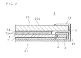
- FIG. 1 is a perspective view of a display apparatus 1 according to an embodiment; and FIG. 2 is a vertical side section view of the display apparatus 1 .
- the display apparatus 1 is constituted by a liquid-crystal display panel 20 having a display surface 20 a on which an image is displayed, a backlight device 21 located on the back surface of the liquid-crystal display panel 20 , a frame body 11 covering a peripheral part and side surfaces of the display surface 20 a of the liquid-crystal display panel 20 , and a casing 12 covering the back surface side and side surfaces of the backlight device 21 .
- the backlight device 21 includes a light guide plate 6 , a prism sheet 72 and a diffusion sheet 73 located between the liquid-crystal display panel 20 and the light guide plate 6 , and a light irradiation device 3 located at a side part of the light guide plate 6 .
- the liquid-crystal display panel 20 has the shape of a rectangular parallelepiped, and is connected to a liquid-crystal display circuit (not illustrated) for applying a display signal to liquid-crystal elements in the liquid-crystal display panel 20 .
- the light guide plate 6 is a thin plate or sheet formed in a rectangular shape having a substantially uniform thickness using a translucent material.
- the light guide plate 6 is generally made of acrylic resin or the like such as, for example, polycarbonate or PMMA (polymethyl methacrylate resin), but is not limited thereto. Furthermore, the light guide plate 6 may be provided, at an end thereof, with a light guiding part described in the prior art.
- the light guide plate 6 is so arranged that one end face thereof is opposed to the light irradiation device 3 , which will be described later, and that one main surface is opposed to the back surface of the liquid-crystal display panel 20 , the one main surface outputting the light entering from the one end face and being guided to the middle.
- a number of concave and convex patterns are formed by a molding process such as heat transfer, so that the light traveling inside the light guide plate 6 is reflected to the side of the one main surface.
- a reflection sheet 71 for reflecting light to the light guide plate 6 is placed on the opposite side of the liquid-crystal display panel 20 of the light guide plate 6 .
- the prism sheet 72 and the diffusion sheet 73 are so arranged as to cover the main surface (light emitting surface) of the light guide plate 6 .
- the prism sheet 72 serves to enhance the light concentration of the light emitted from the light emitting surface of the light guide plate 6 in the direction of the liquid-crystal display panel 20 .
- the diffusion sheet 73 diffuses the incident light so as to reduce the luminance unevenness in the light outputted from the prism sheet 72 , and outputs the light to the back surface of the liquid-crystal display panel 20 .
- the light irradiation device 3 is formed in a rectangular shape, and has a plurality of light emitting elements 4 that emit light.
- the casing 12 includes a rectangular bottom plate and side plates rising from four sides of the bottom plate to the liquid-crystal display panel 20 side, and forms a box-like shape with the liquid-crystal display panel 20 side being open.
- the frame body 11 includes: a frame having the shape of a rectangular picture frame, which covers the peripheral part of the liquid-crystal display panel 20 at the display surface 20 a side; and side plates rising from four sides forming the outer circumference of the frame to the liquid-crystal display panel 20 side.
- the reflection sheet 71 , the light guide plate 6 , the prism sheet 72 and the diffusion sheet 73 are layered, while the light irradiation device 3 is placed at a side part of the light guide plate 6 .
- the liquid-crystal display panel 20 is placed on the diffusion sheet 73 , the frame body 11 is put over the display surface 20 a side of the liquid-crystal display panel 20 , and the ends of the side plates of the frame body 11 are fitted and fixed to the end of the side plates of the casing 12 , to assembly the display apparatus 1 .
- the light guide plate 6 and the light irradiation device 3 constitute a backlight device of an edge light type in the state of being accommodated in the frame body 11 and casing 12 . It is to be noted that a spacer 13 may appropriately be used so that components accommodated inside are stable.
- FIG. 3 is a perspective view of the light irradiation device 3 ;
- FIG. 4 is an exploded perspective view of the light irradiation device 3 ;
- FIG. 5 is a front view of the light irradiation device 3 ;
- FIG. 6 is a section view of the light irradiation device 3 cut along a cross section A-A illustrated in FIG. 5 ;
- FIG. 7 is a section view cut along a cross section B-B illustrated in FIG. 5 .
- the light irradiation device 3 includes a substrate 32 on which a plurality of light emitting elements 4 are arranged, as well as a reinforcement plate 31 and a plate member 33 for reinforcing the substrate 32 .
- the substrate 32 has a rectangular shape, and a plurality of light emitting elements 4 , 4 , . . . are arranged side by side from one end to the other end in the longitudinal direction of one end face 32 a , while convex parts 32 c , 32 c projecting from the one end face 32 a are formed at the above-described one and the other ends.
- Each of the light emitting elements 4 , 4 . . . is a single LED chip, which is smaller than a packaged LED and can be arranged at an end face of a thin substrate.
- each of the light emitting elements 4 , 4 . . . has a configuration in which a diode is located on an insulator.
- Connecting lines 42 , 43 for connection to the light emitting elements 4 , 4 , . . . are provided over the areas from the one and other ends of one end face 32 a to the respective both ends of a main surface 32 b .
- the hatched portions are insulation-coated.
- the both ends of the connecting line 42 are not insulation-coated, and connecting terminals 42 a , 42 b are exposed.
- the both ends of the connecting line 43 are not insulation-coated, and connecting terminals 43 a , 43 b are exposed.
- the connecting terminals 42 b and 43 b are silver-plated.
- an insulation-coated connecting line 44 is provided on the main surface 32 b , while connecting terminals 44 a and 44 b that are not insulation-coated are exposed at both ends of the connecting line 44 .
- the one end face 32 a may correspond to one end face in the short direction, and the light emitting elements 4 , 4 . . . may be arranged on the one end face along the longitudinal direction.
- the substrate 32 As a material for the substrate 32 , a metal material with preferable thermal conductivity such as aluminum or aluminum alloy may be used.
- the substrate 32 made of such a material is suitable for eliminating heat generated at the light emitting elements 4 , 4 . . . .
- the substrate 32 may preferably have a thickness of, for example, in the range from approximately 0.3 mm to approximately 1.0 mm, which contributes to thinning of the light irradiation device 3 . Contrary to the thickness of the substrate 32 , the main surface 32 b of the substrate 32 is configured to have a sufficiently large dimension such as, for example, 10 mm ⁇ 160 mm.
- the light emitting elements 4 , 4 . . . are insulated from the substrate 32 by the respective insulators included therein.
- the substrate 32 may be a glass-epoxy substrate as long as the light emitting elements 4 , 4 . . . are ensured to have a heat dissipating property.
- the substrate 32 may also be
- FIG. 8 is a perspective view of an insulator sheet 8 for interconnection used for the substrate 32 .
- the connecting lines 42 , 43 and 44 described above are located on the rectangular insulator sheet 8 , while the insulator sheet 8 is fixed by bonding it onto the main surface 32 b of the substrate 32 .
- Attachments 8 a , 8 a extending from one end of the insulator sheet 8 are wrapped and fixed onto a main surface on the opposite side of the main surface 32 b .
- the use of the insulator sheet 8 allows the connecting lines 42 , 43 , 44 and the like to easily be provided on the substrate 32 . Furthermore, though it is configured in the case of the insulator sheet 8 illustrated in FIG.
- connecting terminals 42 b and 43 b are provided at both ends on the one end face 32 a
- portions provided with the connecting lines 42 , 43 , 44 and the like may be configured to have an insulating property by partly being coated with glass or the like, while sufficiently ensuring the heat dissipating property of the substrate 32 .
- the light emitting elements 4 , 4 . . . are serially connected by wires 41 , 41 . . . that are electric connection lines for carrying electric current to the light emitting elements 4 , 4 . . . , while the light emitting elements 4 , 4 located at both ends are connected to the connecting terminals 42 b , 43 b through wires 41 , 41 .
- a translucent sealing material 5 for sealing the light emitting elements 4 , 4 . . . and the wires 41 , 41 . . . is adhered to the one end face 32 a , and fills between the convex parts 32 c and 32 c .
- the sealing material 5 fills from base ends of the convex parts 32 c , 32 c (i.e. the one end face 32 a ) to respective positions slightly lower than the tip ends of the convex parts 32 c , 32 c . In other words, the sealing material 5 fills to a midway part of each of the convex parts 32 c , 32 c . It is also possible to provide connecting terminals between the light emitting elements 4 , 4 . . . and to use the wires 41 , 41 . . . to connect the light emitting elements 4 , 4 . . . with one another through the connecting terminals.
- a fluorescent sheet 51 is placed between the sealing material 5 and an end face 6 a of the light guide plate 6 (see FIG. 7 ).
- the fluorescent sheet 51 the light generated at the light emitting elements 4 , 4 . . . is wavelength-converted into light of a desired color, e.g., white light. It is also possible not to employ the fluorescent sheet 51 by making the sealing material 5 contain a fluorescent substance. It is to be noted that the sealing material 5 may be a material not containing a fluorescent substance and the fluorescent sheet 51 may also be unnecessary when the light emitting elements 4 , 4 . . . are configured to have surfaces including a fluorescent substance and the light emitting elements 4 , 4 . . . emit light of a desired wavelength.
- the reinforcement plate 31 includes a side plate 31 c formed by bending an end of a bottom plate 31 b serving as a rectangular main surface to the substrate 32 side, and has an L-shaped cross section.
- the side plate 31 c may also be bent toward the opposite side of the substrate 32 side. However, by bending the side plate 31 c toward the substrate 32 side as illustrated, the ends of the substrate 32 and plate member 33 can be in contact with the side plate 31 c during assembly, which improves the manufacturability.
- One end of the reinforcement plate 31 corresponding to the one end face 32 a side of the substrate 32 protrudes from the one end face 32 a of the substrate 32 , and also protrudes further than the tip end faces of the convex parts 32 c , 32 c of the substrate 32 .
- a light reflection layer 31 d is located at the periphery of the bottom plate 31 b of the reinforcement plate 31 at the one end face 31 a side.
- the dimension in the longitudinal direction of the light reflection layer 31 b is equal to or larger than the distance between the convex parts 32 c and 32 c of the substrate 32 , while the dimension in the short direction thereof is equal to or larger than the distance between the one end face 31 a of the reinforcement plate 31 and the one end face 32 a of the substrate 32 .
- the light reflection layer 31 d is formed by white resist printing, silver plating, polishing or the like.
- a metal material such as stainless steel which has high strength and rigidity may preferably be used.
- the reinforcement plate 31 itself to have a thickness of approximately 0.2 mm for example, in order to reduce the thickness of the light irradiation device 3 , and also to be made of a material having high strength and rigidity. Note that ceramic may be used as the material for the reinforcement plate 31 .
- the plate member 33 has a rectangular shape from which portions on both ends are cut out so as to expose the connecting terminals 42 a , 43 a , 44 a and 44 b .
- One end of the plate member 33 corresponding to the one end face 32 a side of the substrate 32 protrudes from the one end face 32 a of the substrate 32 , and also protrudes further than the tip end faces of the convex parts 32 c , 32 c of the substrate 32 .
- a light reflection layer 33 d is located at the periphery of the main surface of the plate member 33 facing the substrate 32 on the side of one end face 33 a of the plate member 33 .
- the dimension in the longitudinal direction of the light reflection layer 33 d is equal to or larger than the distance between the convex parts 32 c and 32 c of the substrate 32 , while the dimension in the short direction thereof is equal to or larger than the distance between the one end face 33 a of the plate member 33 and the one end face 32 a of the substrate 32 .
- a metal material having good thermal conductivity such as aluminum or aluminum alloy may preferably be used, which is suitable as a heat transfer path for the heat generated at the substrate 32 .
- the plate member 33 it is preferable for the plate member 33 to have a thickness of, for example, approximately 0.1 mm, which contributes to reduction in the thickness of the light irradiation device 3 .
- ceramic may be used as the material for the plate member 33 .
- the substrate 32 , the reinforcement plate 31 and the plate member 33 are integrated by bonding the main surfaces thereof with one another using an adhesive or the like.
- the adhesive to be used may preferably have high thermal conductivity. It is also possible to first integrate the substrate 32 , the reinforcement plate 31 and the plate member 33 together and then a sealing material 5 fills to the one end face 32 a , which also allows the sealing material 5 to be adhered not only to the one end face 32 a but also to the protruding portions of the reinforcement plate 31 and plate member 33 protruding from the one end face 32 a , enhancing the adhering strength of the sealing material 5 .
- two through holes 3 a , 3 b penetrating the light irradiation device 3 are formed, thereby ensuring alignment of the substrate 32 , the reinforcement plate 31 and the plate member 33 using the through holes 3 a , 3 b .
- the through holes 3 a , 3 b can also be utilized as holes for fastening members such as screws to pass through when the light irradiation device 3 is attached to the casing 12 .
- connection terminals 4 b and 43 b of the light irradiation device 3 are connected to a power supply through a switch element, a smoothing circuit and the like (not illustrated).
- the switch element is turned on to light up the light emitting elements 4 , 4 . . . of the light irradiation device 3 .
- the translucent sealing material 5 passes through the translucent sealing material 5 and is outputted toward the normal direction of the one end face 32 a (the light guide plate 6 side), while a part of the light is reflected by the light reflection layer 31 d of the reinforcement plate 31 and the light reflection layer 33 d of the plate member 33 , and is outputted toward the normal direction of the one end face 32 a.
- the light irradiation device 3 irradiates one end face 6 a of the light guide plate 6 opposed to the one end face 32 a with light.
- the light entering from the one end face 6 a of the light guide plate 6 and guided to the middle part is outputted from the main surface of the light guide plate 6 .
- the light outputted from a surface opposite from the main surface of the light guide plate 6 is reflected by the reflection sheet 71 and is outputted from the main surface.
- the light outputted from the main surface of the light guide plate 6 is improved in its light concentration in the direction of the liquid-crystal display panel 20 by the prism sheet 72 and is reduced in its luminance unevenness by the diffusion sheet 73 , and then enters the back surface of the liquid-crystal display panel 20 .
- the liquid-crystal elements are controlled by the display signal applied from the liquid-crystal display circuit, and the light entering the back surface of the liquid-crystal display panel 20 is, for example, deflected by the liquid-crystal elements to form an image and display the image on the display surface 20 a.
- the substrate 32 has a rectangular shape, the light emitting elements 4 , 4 . . . are arranged on the one end face 32 of the substrate 32 , and the translucent sealing material 5 is adhered to the one end face 32 a to seal the light emitting elements 4 , 4 . . . . Accordingly, the thickness of the light irradiation device 3 can be reduced, while the heat generated at the light emitting elements 4 , 4 . . . is transferred to the substrate 32 for heat dissipation. Even with the substrate 32 having a reduced thickness, the heat dissipation performance of the substrate 32 can be maintained or enhanced when the dimension of the substrate 32 is increased in the direction intersecting the one end face 32 a of the substrate 32 .
- the sealing material 5 is used to seal the wires 41 , 41 . . . for carrying electric current to the light emitting elements 4 , 4 . . . , thereby protecting the light emitting elements 4 , 4 . . . and the wires 41 , 41 . . . .
- the reinforcement plate 31 is bonded to one surface of the substrate 32 , and protrudes from the one end face 32 a of the substrate 32 .
- the sealing material 5 is adhered to the portion of the reinforcement plate 31 protruding from the one end face 32 a .
- the reinforcement plate 31 can enhance the strength of the light irradiation device 3 , while securely holding the sealing material 5 .
- the light reflection layer 31 d is located at the portion of the reinforcement plate 31 protruding from the one end face 32 a , the light generated at the light emitting elements 4 , 4 . . . is reflected by the light reflection layer 31 d and thus a large amount of light can be emitted. Moreover, the light generated at the light emitting elements 4 , 4 . . . can also be reflected by the light reflection layer 33 d of the plate member 33 , so that a large amount of light can be emitted.
- the reinforcement plate 31 has the side plate 31 c bent at the other end face side of the substrate 32 , thereby enhancing the strength of the light irradiation device 3 .
- the plate member 33 is adhered to the substrate 32 , and protrudes from the one end face 32 a of the substrate 32 .
- the sealing material 5 is adhered to the portion of the plate member 33 protruding from the one end face 32 a .
- the plate member 33 makes the heat dissipation performance preferable, while securely holding the sealing material 5 .
- the convex parts 32 c , 32 c projecting from one end face 32 a are provided on both ends of the one end face 32 a of the substrate 32 a .
- the sealing material 5 fills to a midway part of each of the convex parts 32 c , 32 c . Therefore, the end face of the light guide plate 6 or the like arranged to be opposed to the light irradiation device 3 makes contact with the convex parts 32 c , 32 c , which can prevent the end face of the light guide plate 6 or the like from directly being in contact with the sealing material 5 and from applying stress on the light emitting elements 4 , 4 . . . as well as the wires 41 , 41 . . . .
- the reinforcement plate 31 and the plate member 33 protrude further than the convex parts 32 c , 32 c of the substrate 32 , it is possible to use the protruding portions to sandwich the end of the light guide plate 6 or the like between the reinforcement plate 31 and the plate member 33 , which facilitates the positioning of the end of the light guide plate 6 or the like and the light irradiation device 3 .
- the light emitting elements 4 , 4 . . . can emit light.
- the substrate 32 aluminum or aluminum alloy is used for the substrate 32 , thereby achieving high thermal conductivity and preferable heat dissipation performance.
- the reinforcement plate 31 is made by using stainless steel, which can enhance the strength of the light irradiation device 3 .
- FIG. 9 is a schematic view for illustrating a configuration in a case where light irradiation devices 3 are arranged side by side according to a modification. Two light irradiation devices 3 are arranged side by side, while an electric wire 9 a of a lead wire 9 is connected to a connecting terminal 42 a of one light irradiation device 3 , and an electric wire 9 b is connected to a connecting terminal 44 a of the one light irradiation device 3 .
- a connecting terminal 43 a of the one light irradiation device 3 and a connecting terminal 42 a of the other light irradiation device 3 are connected through a short pin 91 a
- a connecting terminal 44 b of the one light irradiation device 3 and a connecting terminal 44 a of the other light irradiation device 3 are connected through a short pin 91 b
- a connecting terminal 43 a and a connecting terminal 44 b of the other light irradiation device 3 are connected with each other through a short pin 92 .
- a plurality of light irradiation devices 3 are connected using the connecting lines 42 , 43 and 44 provided on the substrate 32 , so that power is supplied to the respective light emitting elements 4 , 4 . . . of the light irradiation devices 3 , which can be used while being arranged side by side.
- FIG. 10 is a schematic view illustrating a configuration of a light irradiation device 3 according to another modification.
- light emitting elements 4 , 4 . . . are arranged on one end face 32 a of a substrate 32 , and are sealed with a sealing material 5 , not using a reinforcement plate 31 and a plate member 33 .
- Wires 41 , 41 . . . , connecting lines 42 , 43 , 44 and the like are provided on the substrate 32 as in the embodiment described above.
- the light irradiation device 3 can be manufactured to be even thinner while the number of components required for its configuration is small, thereby reducing the cost.
- FIG. 11 is a schematic view illustrating a configuration of a light irradiation device 3 according to another modification.
- the light irradiation device 3 is so configured that light emitting elements 4 , 4 . . . are arranged on one end face 32 a of a substrate 32 , a sealing material 5 is used to seal the light emitting elements 4 , 4 . . . , and a reinforcement plate 31 is bonded to the substrate 32 , while not using a plate member 33 .
- Wires 41 , 41 . . . , connecting lines 42 , 43 , 44 and the like are provided on the substrate 32 as in the embodiment described above.
- the light irradiation device 3 is made thinner as the plate member 33 is not provided, and the number of components required for its configuration is reduced, thereby reducing the cost.
- the light reflection layer 33 d of the plate member 33 it is also possible to separately provide a light reflection sheet in an arrangement similar to that of the light reflection layer 33 d.
- FIG. 12 is a schematic view illustrating a configuration of a light irradiation device 3 according to another modification.
- the light irradiation device 3 is configured as similar to the embodiment described above, while the tip end faces of convex parts 32 , 32 of the substrate 32 , one end face 31 a of the reinforcement plate 31 and one end face 33 a of the plate member 33 are formed to be flush with one another.
- a sealing material 5 fills to a midway part of each of the convex parts 32 c , 32 c .
- the reinforcement member 31 and the plate member 33 do not protrude from the convex parts 32 c , 32 c of the substrate 32 .
- This modification is effective in the case where an end of the light guide plate 6 or the like cannot be sandwiched between the reinforcement plate 31 and the plate member 33 when assembled, as in the embodiment described above.
- FIG. 13 is a schematic view illustrating a configuration of a light irradiation device 3 according to another modification.
- the light irradiation device 3 is configured similarly to the embodiment described above, while one end face 33 a of the plate member 33 is closer to the side of light emitting elements 4 , 4 . . . than one end face 31 a of the reinforcement plate 31 , and is made flush with convex parts 32 c , 32 c of the substrate 32 .
- This facilitates the light guide plate 6 to be located along the protruding portion of the reinforcement plate 31 and also facilitates alignment of the light guide plate 6 and the light irradiation device 3 .
- the convex parts 32 c , 32 c are located on both ends at the one end face 32 a of the substrate 32 in the embodiment and modifications described above, the present invention is not limited thereto but a convex part may be located at, for example, a middle part or the like in the longitudinal direction of the one end face 32 a . It is also possible not to provide the convex parts 32 c , 32 c . In the case where no convex parts 32 c , 32 c are provided, a mechanism for avoiding collision between the light guide plate 6 or the like and the sealing material 5 may preferably be provided in the device.
Landscapes
- Physics & Mathematics (AREA)
- Engineering & Computer Science (AREA)
- Optics & Photonics (AREA)
- General Physics & Mathematics (AREA)
- General Engineering & Computer Science (AREA)
- Microelectronics & Electronic Packaging (AREA)
- Planar Illumination Modules (AREA)
- Liquid Crystal (AREA)
- Fastening Of Light Sources Or Lamp Holders (AREA)
Abstract
Description
Claims (12)
Applications Claiming Priority (3)
| Application Number | Priority Date | Filing Date | Title |
|---|---|---|---|
| JP2012194307A JP2014049418A (en) | 2012-09-04 | 2012-09-04 | Light irradiation device, backlight device and display apparatus |
| JP2012-194307 | 2012-09-04 | ||
| PCT/JP2013/073497 WO2014038502A1 (en) | 2012-09-04 | 2013-09-02 | Light illumination device, backlight device and display device |
Publications (2)
| Publication Number | Publication Date |
|---|---|
| US20150226408A1 US20150226408A1 (en) | 2015-08-13 |
| US9523483B2 true US9523483B2 (en) | 2016-12-20 |
Family
ID=50237111
Family Applications (1)
| Application Number | Title | Priority Date | Filing Date |
|---|---|---|---|
| US14/426,045 Expired - Fee Related US9523483B2 (en) | 2012-09-04 | 2013-09-02 | Light irradiation device, backlight device and display apparatus |
Country Status (5)
| Country | Link |
|---|---|
| US (1) | US9523483B2 (en) |
| JP (1) | JP2014049418A (en) |
| KR (1) | KR20150047559A (en) |
| CN (1) | CN104603520B (en) |
| WO (1) | WO2014038502A1 (en) |
Families Citing this family (1)
| Publication number | Priority date | Publication date | Assignee | Title |
|---|---|---|---|---|
| JP7807220B2 (en) * | 2021-12-08 | 2026-01-27 | シーシーエス株式会社 | Inspection light irradiation device and inspection system |
Citations (11)
| Publication number | Priority date | Publication date | Assignee | Title |
|---|---|---|---|---|
| CN1612020A (en) | 2003-11-01 | 2005-05-04 | 鸿富锦精密工业(深圳)有限公司 | Back light module assembly |
| JP2006344450A (en) | 2005-06-08 | 2006-12-21 | Matsushita Electric Ind Co Ltd | Linear light source and surface light emitting device |
| JP2007194161A (en) | 2006-01-23 | 2007-08-02 | Matsushita Electric Ind Co Ltd | Linear light source device |
| JP2008053571A (en) | 2006-08-28 | 2008-03-06 | Nichia Chem Ind Ltd | Light emitting device and planar light emitting device using the same |
| WO2008099542A1 (en) | 2007-02-13 | 2008-08-21 | Omron Corporation | Light emitting element and surface area illumination device |
| US20080284308A1 (en) * | 2006-11-27 | 2008-11-20 | Siew It Pang | Low profile and high efficiency lighting device for backlighting applications |
| US20090086507A1 (en) * | 2007-09-28 | 2009-04-02 | Fujifilm Corporation | Planar lighting device |
| JP2009199871A (en) | 2008-02-21 | 2009-09-03 | Mitsubishi Electric Corp | Surface light source device, and display device using surface light source device |
| CN101546063A (en) | 2008-03-27 | 2009-09-30 | 深圳帝光电子有限公司 | Ultra thin type LCD use backlight module taking LED as light source |
| JP2010109321A (en) | 2008-09-30 | 2010-05-13 | Toyoda Gosei Co Ltd | Light emitting device, and manufacturing method thereof |
| US7736016B2 (en) * | 2007-10-25 | 2010-06-15 | Toyoda Gosei Co., Ltd. | Light source unit |
Family Cites Families (3)
| Publication number | Priority date | Publication date | Assignee | Title |
|---|---|---|---|---|
| JP3928384B2 (en) * | 2001-08-17 | 2007-06-13 | 松下電工株式会社 | LED lighting fixtures |
| JP2007026858A (en) * | 2005-07-15 | 2007-02-01 | Minebea Co Ltd | Surface lighting device |
| JP2009032479A (en) * | 2007-07-26 | 2009-02-12 | Panasonic Corp | Linear light source device and flexible substrate |
-
2012
- 2012-09-04 JP JP2012194307A patent/JP2014049418A/en active Pending
-
2013
- 2013-09-02 US US14/426,045 patent/US9523483B2/en not_active Expired - Fee Related
- 2013-09-02 WO PCT/JP2013/073497 patent/WO2014038502A1/en not_active Ceased
- 2013-09-02 KR KR1020157007265A patent/KR20150047559A/en not_active Withdrawn
- 2013-09-02 CN CN201380046210.8A patent/CN104603520B/en not_active Expired - Fee Related
Patent Citations (12)
| Publication number | Priority date | Publication date | Assignee | Title |
|---|---|---|---|---|
| CN1612020A (en) | 2003-11-01 | 2005-05-04 | 鸿富锦精密工业(深圳)有限公司 | Back light module assembly |
| JP2006344450A (en) | 2005-06-08 | 2006-12-21 | Matsushita Electric Ind Co Ltd | Linear light source and surface light emitting device |
| JP2007194161A (en) | 2006-01-23 | 2007-08-02 | Matsushita Electric Ind Co Ltd | Linear light source device |
| JP2008053571A (en) | 2006-08-28 | 2008-03-06 | Nichia Chem Ind Ltd | Light emitting device and planar light emitting device using the same |
| US20080284308A1 (en) * | 2006-11-27 | 2008-11-20 | Siew It Pang | Low profile and high efficiency lighting device for backlighting applications |
| WO2008099542A1 (en) | 2007-02-13 | 2008-08-21 | Omron Corporation | Light emitting element and surface area illumination device |
| JP2008198460A (en) | 2007-02-13 | 2008-08-28 | Omron Corp | Light emitting element and surface illumination device |
| US20090086507A1 (en) * | 2007-09-28 | 2009-04-02 | Fujifilm Corporation | Planar lighting device |
| US7736016B2 (en) * | 2007-10-25 | 2010-06-15 | Toyoda Gosei Co., Ltd. | Light source unit |
| JP2009199871A (en) | 2008-02-21 | 2009-09-03 | Mitsubishi Electric Corp | Surface light source device, and display device using surface light source device |
| CN101546063A (en) | 2008-03-27 | 2009-09-30 | 深圳帝光电子有限公司 | Ultra thin type LCD use backlight module taking LED as light source |
| JP2010109321A (en) | 2008-09-30 | 2010-05-13 | Toyoda Gosei Co Ltd | Light emitting device, and manufacturing method thereof |
Also Published As
| Publication number | Publication date |
|---|---|
| US20150226408A1 (en) | 2015-08-13 |
| JP2014049418A (en) | 2014-03-17 |
| KR20150047559A (en) | 2015-05-04 |
| CN104603520A (en) | 2015-05-06 |
| WO2014038502A1 (en) | 2014-03-13 |
| CN104603520B (en) | 2017-09-29 |
Similar Documents
| Publication | Publication Date | Title |
|---|---|---|
| JP5236366B2 (en) | Linear light source device and planar illumination device | |
| CN101153979B (en) | Backlight assembly and cover for a compact display apparatus | |
| CN100523954C (en) | Blacklight unit having a heat receiving member | |
| US10424691B2 (en) | Display apparatus having quantum dot unit or quantum dot sheet and method for manufacturing quantum dot unit | |
| JP5113594B2 (en) | Linear light source device and planar illumination device | |
| JP4238921B2 (en) | LIGHTING DEVICE, ELECTRO-OPTICAL DEVICE, AND ELECTRONIC DEVICE | |
| CN104023427B (en) | Lighting device | |
| KR20190034368A (en) | Backlight unit and display device including the same | |
| JP4610312B2 (en) | Light source device and display device having the same | |
| CN105527749B (en) | Planar light source device, display device and electronic equipment | |
| US9182536B2 (en) | Light-source device and display device | |
| US9690039B2 (en) | Light source device and display device | |
| US9523483B2 (en) | Light irradiation device, backlight device and display apparatus | |
| JP5072186B2 (en) | Liquid crystal display | |
| CN107884986B (en) | Display device with quantum dot unit | |
| JP2020091952A (en) | Linear light emitting device and planar light emitting device | |
| KR20150051120A (en) | Light source module and backlight unit having the same | |
| JP4997402B2 (en) | Chip-like point light source device, planar light source device using the same, and liquid crystal display device | |
| CN114008379B (en) | Linear light device | |
| JP2023132396A (en) | Lighting equipment and display equipment | |
| KR102070639B1 (en) | The radiant heat circuit board and the backlight unit having the same | |
| JP5652440B2 (en) | Electro-optical device and electronic apparatus | |
| WO2012111398A1 (en) | Edge-lit lighting device and display device | |
| JP2021168229A (en) | Linear light-emitting member and planar light-emitting device | |
| JP2002107715A (en) | Liquid crystal display device |
Legal Events
| Date | Code | Title | Description |
|---|---|---|---|
| AS | Assignment |
Owner name: OG CORPORATION, JAPAN Free format text: ASSIGNMENT OF ASSIGNORS INTEREST;ASSIGNORS:ONO, KOUJI;SUMI, TAKESHI;REEL/FRAME:035111/0140 Effective date: 20150224 Owner name: T. CHATANI & CO., LTD., JAPAN Free format text: ASSIGNMENT OF ASSIGNORS INTEREST;ASSIGNORS:ONO, KOUJI;SUMI, TAKESHI;REEL/FRAME:035111/0140 Effective date: 20150224 |
|
| AS | Assignment |
Owner name: OG CORPORATION, JAPAN Free format text: CORRECTIVE ASSIGNMENT TO CORRECT THE FIRST ASSIGNEE'S ADDRESS PREVIOUSLY RECORDED AT REEL: 035111 FRAME: 0140. ASSIGNOR(S) HEREBY CONFIRMS THE ASSIGNMENT;ASSIGNORS:ONO, KOUJI;SUMI, TAKESHI;REEL/FRAME:035356/0396 Effective date: 20150224 Owner name: T. CHATANI & CO., LTD., JAPAN Free format text: CORRECTIVE ASSIGNMENT TO CORRECT THE FIRST ASSIGNEE'S ADDRESS PREVIOUSLY RECORDED AT REEL: 035111 FRAME: 0140. ASSIGNOR(S) HEREBY CONFIRMS THE ASSIGNMENT;ASSIGNORS:ONO, KOUJI;SUMI, TAKESHI;REEL/FRAME:035356/0396 Effective date: 20150224 |
|
| STCF | Information on status: patent grant |
Free format text: PATENTED CASE |
|
| FEPP | Fee payment procedure |
Free format text: MAINTENANCE FEE REMINDER MAILED (ORIGINAL EVENT CODE: REM.); ENTITY STATUS OF PATENT OWNER: LARGE ENTITY |
|
| LAPS | Lapse for failure to pay maintenance fees |
Free format text: PATENT EXPIRED FOR FAILURE TO PAY MAINTENANCE FEES (ORIGINAL EVENT CODE: EXP.); ENTITY STATUS OF PATENT OWNER: LARGE ENTITY |
|
| STCH | Information on status: patent discontinuation |
Free format text: PATENT EXPIRED DUE TO NONPAYMENT OF MAINTENANCE FEES UNDER 37 CFR 1.362 |
|
| FP | Lapsed due to failure to pay maintenance fee |
Effective date: 20201220 |