US9520179B1 - Asynchronous FIFO memory with read and write counter circuitry - Google Patents
Asynchronous FIFO memory with read and write counter circuitry Download PDFInfo
- Publication number
- US9520179B1 US9520179B1 US15/205,914 US201615205914A US9520179B1 US 9520179 B1 US9520179 B1 US 9520179B1 US 201615205914 A US201615205914 A US 201615205914A US 9520179 B1 US9520179 B1 US 9520179B1
- Authority
- US
- United States
- Prior art keywords
- read
- write
- flip
- clock
- flop
- Prior art date
- Legal status (The legal status is an assumption and is not a legal conclusion. Google has not performed a legal analysis and makes no representation as to the accuracy of the status listed.)
- Active
Links
Images


Classifications
-
- G—PHYSICS
- G11—INFORMATION STORAGE
- G11C—STATIC STORES
- G11C11/00—Digital stores characterised by the use of particular electric or magnetic storage elements; Storage elements therefor
- G11C11/21—Digital stores characterised by the use of particular electric or magnetic storage elements; Storage elements therefor using electric elements
- G11C11/34—Digital stores characterised by the use of particular electric or magnetic storage elements; Storage elements therefor using electric elements using semiconductor devices
- G11C11/40—Digital stores characterised by the use of particular electric or magnetic storage elements; Storage elements therefor using electric elements using semiconductor devices using transistors
- G11C11/41—Digital stores characterised by the use of particular electric or magnetic storage elements; Storage elements therefor using electric elements using semiconductor devices using transistors forming static cells with positive feedback, i.e. cells not needing refreshing or charge regeneration, e.g. bistable multivibrator or Schmitt trigger
- G11C11/413—Auxiliary circuits, e.g. for addressing, decoding, driving, writing, sensing, timing or power reduction
- G11C11/417—Auxiliary circuits, e.g. for addressing, decoding, driving, writing, sensing, timing or power reduction for memory cells of the field-effect type
- G11C11/419—Read-write [R-W] circuits
-
- G—PHYSICS
- G06—COMPUTING OR CALCULATING; COUNTING
- G06F—ELECTRIC DIGITAL DATA PROCESSING
- G06F5/00—Methods or arrangements for data conversion without changing the order or content of the data handled
- G06F5/06—Methods or arrangements for data conversion without changing the order or content of the data handled for changing the speed of data flow, i.e. speed regularising or timing, e.g. delay lines, FIFO buffers; over- or underrun control therefor
- G06F5/10—Methods or arrangements for data conversion without changing the order or content of the data handled for changing the speed of data flow, i.e. speed regularising or timing, e.g. delay lines, FIFO buffers; over- or underrun control therefor having a sequence of storage locations each being individually accessible for both enqueue and dequeue operations, e.g. using random access memory
- G06F5/12—Means for monitoring the fill level; Means for resolving contention, i.e. conflicts between simultaneous enqueue and dequeue operations
-
- G—PHYSICS
- G11—INFORMATION STORAGE
- G11C—STATIC STORES
- G11C7/00—Arrangements for writing information into, or reading information out from, a digital store
- G11C7/10—Input/output [I/O] data interface arrangements, e.g. I/O data control circuits, I/O data buffers
- G11C7/1051—Data output circuits, e.g. read-out amplifiers, data output buffers, data output registers, data output level conversion circuits
-
- G—PHYSICS
- G06—COMPUTING OR CALCULATING; COUNTING
- G06F—ELECTRIC DIGITAL DATA PROCESSING
- G06F2205/00—Indexing scheme relating to group G06F5/00; Methods or arrangements for data conversion without changing the order or content of the data handled
- G06F2205/12—Indexing scheme relating to groups G06F5/12 - G06F5/14
- G06F2205/126—Monitoring of intermediate fill level, i.e. with additional means for monitoring the fill level, e.g. half full flag, almost empty flag
-
- G—PHYSICS
- G11—INFORMATION STORAGE
- G11C—STATIC STORES
- G11C7/00—Arrangements for writing information into, or reading information out from, a digital store
- G11C7/10—Input/output [I/O] data interface arrangements, e.g. I/O data control circuits, I/O data buffers
- G11C7/1051—Data output circuits, e.g. read-out amplifiers, data output buffers, data output registers, data output level conversion circuits
- G11C7/1057—Data output buffers, e.g. comprising level conversion circuits, circuits for adapting load
-
- G—PHYSICS
- G11—INFORMATION STORAGE
- G11C—STATIC STORES
- G11C7/00—Arrangements for writing information into, or reading information out from, a digital store
- G11C7/10—Input/output [I/O] data interface arrangements, e.g. I/O data control circuits, I/O data buffers
- G11C7/1051—Data output circuits, e.g. read-out amplifiers, data output buffers, data output registers, data output level conversion circuits
- G11C7/106—Data output latches
-
- G—PHYSICS
- G11—INFORMATION STORAGE
- G11C—STATIC STORES
- G11C7/00—Arrangements for writing information into, or reading information out from, a digital store
- G11C7/10—Input/output [I/O] data interface arrangements, e.g. I/O data control circuits, I/O data buffers
- G11C7/1078—Data input circuits, e.g. write amplifiers, data input buffers, data input registers, data input level conversion circuits
-
- G—PHYSICS
- G11—INFORMATION STORAGE
- G11C—STATIC STORES
- G11C7/00—Arrangements for writing information into, or reading information out from, a digital store
- G11C7/22—Read-write [R-W] timing or clocking circuits; Read-write [R-W] control signal generators or management
Definitions
- the invention relates to digital memory devices, and more particularly to a FIFO memory device that provides accurate read and write counts.
- FIFO First In, First Out
- FIFO refers to the organization and manipulation of data according to time and prioritization. Each data item is stored in a queue data structure. The first data added to the queue will be the first data to be removed. Processing proceeds sequentially in this same order.
- FIFO data storage has widespread application in data processing hardware.
- a synchronous FIFO uses the same clock for reading and writing data.
- An asynchronous FIFO uses separate clocks for reading and writing.
- an asynchronous FIFO refers to a FIFO design where data values are written to a FIFO buffer from one clock domain and the data values are read from the same FIFO buffer from another clock domain, where the two clock domains are asynchronous to each other.
- Asynchronous FIFOs have various applications, and are used to safely pass multi-bit data words from one clock domain to another clock domain.
- a difficulty with asynchronous FIFOs is providing an accurate count of the words currently being stored.
- Status signals such as “Full” and “Empty” are used, but in conventional FIFOs, read and write counts are merely estimates of the number of words in the FIFO. Delays from reading to write data count and from writing to read data count depend on the relative clock frequencies of read and write clocks.
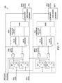
- FIG. 1 illustrates a FIFO having read count and write count circuitry in accordance with the invention.
- FIG. 2 illustrates read count circuitry for a FIFO whose write clock is faster than the read clock.
- FIG. 3 illustrates the pulse generators of FIG. 2 .
- FIG. 4 illustrates the write count circuitry for a FIFO whose write clock is faster than the read clock.
- FIG. 5 illustrates write count circuitry for a FIFO whose read clock is faster than the write clock.
- FIG. 6 illustrates read count circuitry for a FIFO whose read clock is faster than the write clock.
- FIG. 7 illustrates the write count and read count circuitry for a FIFO whose clocks run at equal frequencies.
- FIGS. 8A and 8B are timing diagrams of an example of operation of the read count and write count circuits of FIGS. 2 and 4 .
- FIGS. 9A and 9B are timing diagrams of an example of operation of the read count and write count circuits of FIGS. 5 and 6 .
- the following description is directed to a FIFO memory unit (referred to herein as a “FIFO”) with asynchronous read and write clocks.
- FIFO FIFO memory unit
- the FIFO has special read and write count circuitry to maintain accurate read and write counts.
- an asynchronous FIFO uses separate clocks for reading and writing. Data words are placed into a write port of the FIFO by control signals in one clock domain. These data words are read from another port of the same FIFO by control signals from a second clock domain.
- a difficulty associated with asynchronous FIFOs is finding a reliable means to track the read and write counts of the number of words stored in the FIFO.
- Various data processing applications may benefit from an accurate count of data words written to or read from the FIFO at any given time.
- FIG. 1 illustrates an asynchronous FIFO 100 , which comprises conventional data storage and control logic, as well as read count circuit 101 and write count circuit 102 in accordance with the invention.
- the FIFO data storage may be static random access memory (SRAM) or any other suitable form of data storage.
- SRAM static random access memory
- a dual-port SRAM is usually used, where one port is dedicated to writing and the other to reading.
- Control signals relevant to the invention are shown; FIFO 100 may have various other control signals such as pointers.
- FIFO 100 is loaded from the Write Data bus 105 when the Write Enable signal is active on the rising edge of the Write clock signal.
- Write count circuit 102 increments a Write Count value. It also increments a Read Count value synchronous to the Read Clock signal, a minimal number of Read Clock cycles later.
- FIFO 100 is read from the Read Data bus 107 when the Read Enable signal is active on the rising edge of the Read Clock signal.
- Read Count circuit 101 decrements the Read Count value. It also decrements a write Count synchronous to the Write Clock signal, a minimal number of Write clock cycles later.
- read count circuit 101 and write count circuit 102 provide accurate read and write counts. Neither the read count circuit 101 nor the write count circuit 102 skips counts. The counts are accurate even with time-contiguous data transfers.
- FIG. 2 illustrates the read count circuit 101 .
- the primary focus of circuit 101 is generating a “read synchronized write pulse vector”, whose bits are added to increment a read counter 21 .
- the FIFO's clock and enable signals are used as inputs to this circuitry.
- the FIFO's write clock frequency is higher than that of the read clock. That is, the write clock is faster than the read clock.
- a cascade of flip-flops is configured as a shift register 22 , the flip-flops sharing the same write clock.
- the flip-flops are D-type flip-flops with set-reset. This is an asynchronous reset, which clears (resets) the flip-flop immediately, without waiting for a rising clock edge.
- the output (Q) of each flip-flop is connected to the data (D) input of the next flip-flop in the cascade.
- the result is a shift register 22 that shifts by one position the ‘bit array’ stored in it, ‘shifting in’ the data present at its input and ‘shifting out’ the last bit in the array, at each positive transition of the write clock input.
- the serial input and last output of shift register 22 are connected to create a ‘circular shift register’.
- the width of the shift register 22 (the number of flip-flops) may vary. As explained below, this width (SW+1) is based on the ratio of frequencies of write clock to read clock.
- the shift register 22 is “one-hot” in the sense that the legal combinations of bit values are only those with a single high (1) bit and all the others low (0).
- Shift register 22 runs continuously. Each flip-flop has associated AND logic 23 at its output. The shift register outputs are bit-wise ANDed with the write enable signal.
- the result of the AND logic is a Write Pulse Vector [SW:0].
- SW:0 Write Pulse Vector
- the bits in this vector are also “one-hot”.
- Each AND element 23 has an associated pulse generator 24 at its output. The outputs of the AND elements 23 are fed to the associated pulse generators 24 , synchronous to the read clock.
- FIG. 3 illustrates a pulse generator 24 , of which there are three or more in FIG. 2 .
- the input pulse is delivered to a first flip-flop 31 as a clock signal, with the read clock providing the clock signal to flip-flops 32 and 33 .
- a “1” value is provided to the data input of flip-flop 31 .
- Flip-flops 32 and 33 receive the output of the preceding flip-flop. The result is a write pulse vector that is now read-synchronized.
- the bits of the read-synchronized Write Pulse Vector are summed in adder 25 .
- the result is a Write Pulse sum that increments the Read Counter 21 .
- the Read Enable signal decrements the Read Counter 21 by 1 each time it occurs, synchronous with the read clock.
- FIG. 4 illustrates the write count circuitry 102 corresponding to the read count circuitry 101 .
- similar circuitry is used for generating the Write Count.
- vector sizes converge to 2 (SW+1), and all the Read and Write signal names have Read and Write swapped.
- Shift registers 42 , AND elements 43 , pulse generators 44 , adder 45 and write counter 41 are configured and operate similarly to like elements described above for the read count circuitry 101 .
- the vectors whose size determine the size of the shift register and the number of associated AND elements and pulse generators may be referred to as [SW:0] for the write counter vectors and [SR:0] for the read counter vectors.
- the equations that determine the vector sizes are determined by the Write to Read Clock frequency ratios and are calculated as follows:
- RATIO is the Write Clock frequency divided by the Read Clock frequency.
- the implemented RATIO can never be less than 0.8.
- a 2.5 multiplier in the following equations guarantees no overlapping in the Write Pulse Vector. Any value less than 0.8 does not satisfy that criteria.
- RATIO_25 W RATIO_ W ⁇ 2.5+0.499
- RATIO_25 R RATIO_ R ⁇ 2.5+0.499
- SHIFT_ W Integer(RATIO_25 W ).
- SW is this number ⁇ 1.
- SHIFT_ R Integer(RATIO_25 R )
- SR this number ⁇ 1.
- the number of Adder bits feeding the Read Counter 21 is Log 2(SHIFT_W) rounded up.
- the number of Adder bits feeding the Write Counter 41 is Log 2(SHIFT_R) rounded up.
- the write clock is at higher frequency than the read clock. If the read clock is at higher frequency than the write clock, the write count circuitry would look like that of FIG. 2 but with the “read” and “write” labels swapped. Similarly, the read count circuitry would like that of FIG. 4 , but with the “read” and “write” labels swapped. Regardless of which clock is faster, the vector size for the clock with the lower frequency (the slower clock) is always the same and converges to 2.
- FIG. 5 illustrates write count circuitry 500 , modified for FIFO's having their read clock faster than their write clock.
- FIG. 6 illustrates the corresponding read count circuitry.
- shift registers, AND elements, pulse generators, adder and read and write counters are configured and operate similarly to like elements described above.
- the vector size converges to 2 (SW+1).
- FIG. 7 illustrates the circuitry for both the read and write counts of an asynchronous FIFO whose clocks have equal frequencies.
- FIGS. 8A and 8B are timing diagrams of an example of operation of the circuit of FIGS. 2-4 . That, is the write clock is faster than the read clock. In this example, the ratio of the write clock to the read clock is 4:3 or 1.333. In the time period shown, four data words are read in and four data words are read out of the FIFO.
- FIGS. 8A and 8B the outputs of the AND elements and the pulse generators for the write count and read count circuitry are also shown.
- values for the write pulse vector and the values for the read synchronized write pulse vector are shown.
- values for the read pulse vector and the values for the write synchronized read pulse vector are shown.
- the read count from read counter 21 , and the write count from counter 41 are accurate during this time period.
- FIGS. 9A and 9B are timing diagrams for another example of asynchronous clocks.
- the write clock is slower than the read clock.
- the write to read ratio is 3:4.
- four data words are written to and four data words are read from the FIFO.
- the slower clock has a shift register size of 2, or SW+1.
- FIFO 100 is operable with any clock frequency ratio, as well as with frequency matching asynchronous Read/Write Clocks. It yields a significantly small turnaround time for the count values in response to their respective enable inputs.
Landscapes
- Engineering & Computer Science (AREA)
- Theoretical Computer Science (AREA)
- Physics & Mathematics (AREA)
- General Engineering & Computer Science (AREA)
- General Physics & Mathematics (AREA)
- Microelectronics & Electronic Packaging (AREA)
- Computer Hardware Design (AREA)
- Synchronisation In Digital Transmission Systems (AREA)
Abstract
Description
RATIO_W=RATIO if RATIO≧0.8, else RATIO_W=0.8
RATIO_R=1/RATIO if 1/RATIO≧0.8, else RATIO_R=0.8
RATIO_25W=RATIO_W×2.5+0.499
RATIO_25R=RATIO_R×2.5+0.499
SHIFT_W=Integer(RATIO_25W).
Referring again to
SHIFT_R=Integer(RATIO_25R)
Referring again to
RATIO_W=1.333
RATIO_R=0.8
RATIO_25W=3.831
RATIO_25R=2.499
SHIFT_W=4
SHIFT_R=2
RATIO_W=0.8
RATIO_R=1.333
RATIO_25W=2.499
RATIO_25R=3.831
SHIFT_W=2
SHIFT_R=4
Claims (6)
Priority Applications (1)
| Application Number | Priority Date | Filing Date | Title |
|---|---|---|---|
| US15/205,914 US9520179B1 (en) | 2016-07-08 | 2016-07-08 | Asynchronous FIFO memory with read and write counter circuitry |
Applications Claiming Priority (1)
| Application Number | Priority Date | Filing Date | Title |
|---|---|---|---|
| US15/205,914 US9520179B1 (en) | 2016-07-08 | 2016-07-08 | Asynchronous FIFO memory with read and write counter circuitry |
Publications (1)
| Publication Number | Publication Date |
|---|---|
| US9520179B1 true US9520179B1 (en) | 2016-12-13 |
Family
ID=57484009
Family Applications (1)
| Application Number | Title | Priority Date | Filing Date |
|---|---|---|---|
| US15/205,914 Active US9520179B1 (en) | 2016-07-08 | 2016-07-08 | Asynchronous FIFO memory with read and write counter circuitry |
Country Status (1)
| Country | Link |
|---|---|
| US (1) | US9520179B1 (en) |
Citations (1)
| Publication number | Priority date | Publication date | Assignee | Title |
|---|---|---|---|---|
| US20030107937A1 (en) * | 2001-12-11 | 2003-06-12 | Williams Kenneth L. | Asynchronous FIFO memory having built-in self test logic |
-
2016
- 2016-07-08 US US15/205,914 patent/US9520179B1/en active Active
Patent Citations (1)
| Publication number | Priority date | Publication date | Assignee | Title |
|---|---|---|---|---|
| US20030107937A1 (en) * | 2001-12-11 | 2003-06-12 | Williams Kenneth L. | Asynchronous FIFO memory having built-in self test logic |
Similar Documents
| Publication | Publication Date | Title |
|---|---|---|
| US7116601B2 (en) | Pseudo-synchronization of the transportation of data across asynchronous clock domains | |
| US9330740B1 (en) | First-in first-out circuits and methods | |
| US5896052A (en) | Methods to avoid instability | |
| US8471607B1 (en) | High-speed frequency divider architecture | |
| US10133549B1 (en) | Systems and methods for implementing a synchronous FIFO with registered outputs | |
| US7668022B2 (en) | Integrated circuit for clock generation for memory devices | |
| CN110442320B (en) | FIFO circuit for double data rate memory system | |
| CN107544616B (en) | Method and apparatus for phase aligned 2X frequency clock generation | |
| JP2004062630A (en) | FIFO memory and semiconductor device | |
| US9520179B1 (en) | Asynchronous FIFO memory with read and write counter circuitry | |
| US5663994A (en) | Two cycle asynchronous FIFO queue | |
| US5033066A (en) | Event tagging time delay | |
| US8363766B2 (en) | Device and method of synchronizing signals | |
| US20060031700A1 (en) | Circuit and method for generating clock signals for clocking digital signal processor and memory | |
| US6377071B1 (en) | Composite flag generation for DDR FIFOs | |
| US10469242B2 (en) | Mulit-lane synchronous reset for coherent receivers | |
| US10090842B2 (en) | Frequency divider regarding variable division ratio | |
| CN114095015B (en) | Deburring clock frequency division circuit, method and terminal | |
| US5963056A (en) | Full and empty flag generator for synchronous FIFOs | |
| US6680990B1 (en) | Elastic integrated circuit | |
| US4796225A (en) | Programmable dynamic shift register with variable shift control | |
| Bhatnagar et al. | Design and implementation of an efficient buffer management system for network on chip routers | |
| US5249154A (en) | Data access controller and method | |
| US6836447B2 (en) | Circuit and method for synchronizing multiple digital data paths | |
| KR950002087B1 (en) | Resister circuit with fifo function |
Legal Events
| Date | Code | Title | Description |
|---|---|---|---|
| FEPP | Fee payment procedure |
Free format text: PAYOR NUMBER ASSIGNED (ORIGINAL EVENT CODE: ASPN); ENTITY STATUS OF PATENT OWNER: SMALL ENTITY |
|
| AS | Assignment |
Owner name: THE GOVERNMENT OF THE UNITED STATES OF AMERICA, AS Free format text: CONFIRMATORY LICENSE;ASSIGNOR:SOUTHWEST RESEARCH INSTITUTE;REEL/FRAME:039337/0165 Effective date: 20160713 |
|
| AS | Assignment |
Owner name: SOUTHWEST RESEARCH INSTITUTE, TEXAS Free format text: ASSIGNMENT OF ASSIGNORS INTEREST;ASSIGNOR:JOHNSON, MARK A.;REEL/FRAME:039246/0054 Effective date: 20160713 |
|
| STCF | Information on status: patent grant |
Free format text: PATENTED CASE |
|
| MAFP | Maintenance fee payment |
Free format text: PAYMENT OF MAINTENANCE FEE, 4TH YR, SMALL ENTITY (ORIGINAL EVENT CODE: M2551); ENTITY STATUS OF PATENT OWNER: SMALL ENTITY Year of fee payment: 4 |
|
| MAFP | Maintenance fee payment |
Free format text: PAYMENT OF MAINTENANCE FEE, 8TH YR, SMALL ENTITY (ORIGINAL EVENT CODE: M2552); ENTITY STATUS OF PATENT OWNER: SMALL ENTITY Year of fee payment: 8 |