US9515390B1 - Discrete phased electromagnetic reflector based on two-state elements - Google Patents
Discrete phased electromagnetic reflector based on two-state elements Download PDFInfo
- Publication number
- US9515390B1 US9515390B1 US14/737,283 US201514737283A US9515390B1 US 9515390 B1 US9515390 B1 US 9515390B1 US 201514737283 A US201514737283 A US 201514737283A US 9515390 B1 US9515390 B1 US 9515390B1
- Authority
- US
- United States
- Prior art keywords
- phase
- cell
- cells
- elements
- array
- Prior art date
- Legal status (The legal status is an assumption and is not a legal conclusion. Google has not performed a legal analysis and makes no representation as to the accuracy of the status listed.)
- Expired - Fee Related, expires
Links
Images


Classifications
-
- H—ELECTRICITY
- H01—ELECTRIC ELEMENTS
- H01Q—ANTENNAS, i.e. RADIO AERIALS
- H01Q15/00—Devices for reflection, refraction, diffraction or polarisation of waves radiated from an antenna, e.g. quasi-optical devices
- H01Q15/14—Reflecting surfaces; Equivalent structures
- H01Q15/148—Reflecting surfaces; Equivalent structures with means for varying the reflecting properties
-
- H—ELECTRICITY
- H01—ELECTRIC ELEMENTS
- H01Q—ANTENNAS, i.e. RADIO AERIALS
- H01Q15/00—Devices for reflection, refraction, diffraction or polarisation of waves radiated from an antenna, e.g. quasi-optical devices
- H01Q15/14—Reflecting surfaces; Equivalent structures
- H01Q15/141—Apparatus or processes specially adapted for manufacturing reflecting surfaces
- H01Q15/142—Apparatus or processes specially adapted for manufacturing reflecting surfaces using insulating material for supporting the reflecting surface
-
- H—ELECTRICITY
- H01—ELECTRIC ELEMENTS
- H01Q—ANTENNAS, i.e. RADIO AERIALS
- H01Q19/00—Combinations of primary active antenna elements and units with secondary devices, e.g. with quasi-optical devices, for giving the antenna a desired directional characteristic
- H01Q19/10—Combinations of primary active antenna elements and units with secondary devices, e.g. with quasi-optical devices, for giving the antenna a desired directional characteristic using reflecting surfaces
- H01Q19/104—Combinations of primary active antenna elements and units with secondary devices, e.g. with quasi-optical devices, for giving the antenna a desired directional characteristic using reflecting surfaces using a substantially flat reflector for deflecting the radiated beam, e.g. periscopic antennas
Definitions
- the invention relates generally to electromagnetic radiation reflectors.
- the invention relates to signal reflectors to redirect and/or reshape electromagnetic radiation.
- Radiation reflectors include reflect-arrays, which are known to those skilled in the art of antenna designs as useful for reflecting an electromagnetic wave at various angles by controlling the phase of the elements that compose the array.
- a phased array can be used to control electromagnetic radiation. By controlling the phase of each element within the array, a narrow electromagnetic beam can be formed. By dynamically changing the phase in a way known to those skilled in the art of antenna design, the beam can be steered, as reported by A. J. Fenn et al., “The Development of Phased-Array Radar Technology”, LINCOLN Laboratory Journal, 12 321-340 (2000), available at https://www.ll.mitedu/publications/journal/pdf/vol12_no2/12_2devphasedarray.pdf.
- Reflect-arrays are similar to phased arrays but the elements in the array produce no radiation of their own. Instead, each element is a reflector that reflects a small portion of incident radiation. Often, the elements are designed to be resonant at a given frequency or over a range of frequencies. By controlling the resonance, the phase of the reflected signal can be dynamically controlled into different directions as reported by D. G. Berry et al., “The Reflectarray Antenna”, IEEE Transactions on Antennas and Propagation, 11 645-651 (1963).
- transition between two phases in a reflect-array often occurs over a very narrow range of control parameters. Precise control of the phase of each element can be difficult in relation to the others in order to achieve precise beam steering. Further, due to material losses and resonant component losses, the amplitude of the reflected signal can be dramatically reduced at resonance, which is often an undesirable effect.
- Various exemplary embodiments provide a method and system for controlling the phase (and amplitude) of a reflect-array at any angle while maintaining high reflected amplitude of the signal.
- the proposed two-stage elements provide a simple solution and are easy to implement.
- Other various embodiments alternatively or additionally provide for a broader range of phase control.
- Various exemplary embodiments provide optical control without the electromagnetic interference effect. These can be performed in conjunction with other methods for control. These and other objects are achieved by the invention, embodiments of which comprise a system and method for controlling the phase shift of a reflected electromagnetic signal in a reflect-array by employing a unit cell comprising an element having multiple phase states. Additional aspects and/or advantages of the invention will be set forth in part in the description which follows and, in part, will be obvious from the description, or may be learned by practice of the invention.
- FIGS. 1A and 1B are plot views of idealized step function phase response
- FIG. 2 is a tabular view of phase responses for various states
- FIG. 3 is a tabular view of amplitude and phase responses
- FIGS. 4A and 4B are plot views of phase responses over a range of direction angle values
- FIGS. 5A and 5B are plot views of power responses to reflection angle
- FIGS. 6A and 6B are plot views of phase responses to polar and azimuthal angles
- FIG. 7 is a grid view of wavelength-scale cells
- FIGS. 8A and 8B are phase amplitude responses to frequency
- FIG. 9 is a plot view of phase response to frequency.
- FIG. 10 is an isometric view of a unit cell disposable to form a planar reflective array.
- the components, process steps, and/or data structures may be implemented using various types of operating systems, computing platforms, computer programs, and/or general purpose machines.
- general purpose machines include devices that execute instruction code.
- a hardwired device may constitute an application specific integrated circuit (ASIC) or a field programmable gate array (FPGA) or other related component.
- phase of the reflected wave has discrete values depending on the number of elements in the array that can be controlled in a more stable way.
- Various embodiments provide a method and a system for reflecting an electromagnetic wave with a phase change from that of normal metallic or dielectric materials.
- the phase of the reflected wave can be any number of discrete steps in phase dependent on the number of elements in the reflect-array.
- a principal advantage of exemplary embodiments is that the phase change can be accomplished using any unit-cell structure that has two states.
- phase resolution and dynamic range can be independently controlled. For example, in a simple linear array, a ten-element array can reflect the electromagnetic wave with any one of eleven phase values in one particular direction (normal to the array for example). For elements that have two states of phase shift, given by phases ⁇ 1 and ⁇ 2 , then the eleven phase values will lie between ⁇ 1 and ⁇ 2 .
- Exemplary embodiments enable the control of the phase (and amplitude) of a reflect-array at any angle.
- the angle can be assumed to be normal to the array in the following description.
- Each unit-cell in the array can be assumed to have two phases.
- each unit-cell can be phase ⁇ 1 or phase ⁇ 2 .
- the continuous phase change between ⁇ 1 and ⁇ 2 can be assumed to be infinitely sharp effectively for clarity.
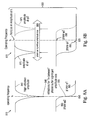
- FIG. 1A shows a diagram view 100 of the step function phase response of a two-phase unit-cell.
- a control parameter represents the abscissa 110 and phase denotes the ordinate 120 .
- Values for the first phase 130 and the second phase 140 are plotted as different constants, with the phase transition at a specified value of the control variable assumed to be infinitely sharp for clarity.
- FIG. 1B shows a diagram view 150 of the step function phase response with transition points for a group of unit-cells and the same abscissa 110 and ordinate 120 .
- Values for the first phase 160 and the second phase 170 are plotted as different constants, with the transitions 180 being responsive to different elements.
- each element can change states at a different setting of the control parameter.
- the phase shift ⁇ n for each element n represents one of two states for any of the N elements.
- the final wave will have any phase between ⁇ 1 and ⁇ 2 with N+1 discrete steps. For example, one can assume that a simple two-element system has a total of three phase states.
- a plurality of elements can reflect many discrete phases. With N elements, one can achieve N+1 discrete phases. Depending on the configuration of phase distribution among the elements, either linear or random phase patterns of the total field can be generated. For example, for six elements with ⁇ 90° of two phase states, a linear phase chirp can be generated if the distribution pattern of each step is given by the array:
- control elements include, but are not limited to, photo-capacitance chips with different capacitance and conductivity controlled by infrared (IR) light intensity, as well as piezoelectric materials and carbon nanotubes (CNT).
- IR infrared
- CNT carbon nanotubes
- N the total number of elements
- ⁇ n the phase shift of the element n
- ⁇ angular frequency
- t time
- the final wave For a wavelet reflected from each of n elements, the final wave has a net phase of approximately eqn. (1) where ⁇ n represents one of two states for any of the N elements. Depending on how many of the N elements are in state ⁇ 1 or in state ⁇ 2 , the final wave has any phase between ⁇ 1 and ⁇ 2 with N+1 discrete steps.
- a simple two-element system has a total of three phase states.
- Table 1 in FIG. 2 shows a tabular listing 200 with particular states and resulting values, together with their resulting phase shift.
- Table 2 in FIG. 3 shows a tabular listing 300 with amplitudes and phase states that yield resulting phase shifts.
- the tabular listing 300 in Table 2 summarizes an example with two elements, two phase states (0° and 90°) and two amplitude states (0.5 and 1).
- the exemplary process can be applied to military fields as well as in civilian; e.g., transmission of radiation with controlled direction, such as beam steering, for nonmilitary use from radio frequency (RF) to infrared (IR), and thus would be of great interest for maritime and aerial navigation, and for weather radars.
- RF radio frequency
- IR infrared
- An advantage of various exemplary embodiments is that the phase can be controlled with simple two-stage elements and that the control can be accomplished without loss of amplitude of the reflected wave.
- Phase resolution depends on the number of elements while dynamic range depends on the phase difference of the two states. Therefore, the resolution and the dynamic range can be independently controlled.
- a side lobe will exist because the system represents a two-element reflect-array where each element has different phases and amplitudes that can be controlled through, but not limited to, photocapacitors with different light intensities.
- phase pattern can also be generated if each element is controlled to acquire a phase of either ⁇ 90° (or ⁇ /2 radians).
- above phase should be added into propagation phase of electromagnetic wave through Huygens-Fresnel Principle:
- E ⁇ ( r ) 1 i ⁇ ⁇ ⁇ ⁇ ⁇ ⁇ E ⁇ ( r ′ ) ⁇ exp ⁇ ( i ⁇ ⁇ k ⁇ ⁇ ⁇ r - r ′ ⁇ ) ⁇ r - r ′ ⁇ ⁇ cos ⁇ ⁇ ⁇ ⁇ d s ′ ( 2 )
- E is the electric field
- ⁇ denotes the surface of the reflector array
- ⁇ is the wavelength of free space
- ⁇ is the polar angle between the surface normal and the observation vector r connecting the observation point to the integration vector r′ on the surface ⁇
- the surface integration includes the areas of two-state elements and the spacing in between where a ⁇ phase shift is assumed due to perfect electric conductor backplane.
- FIGS. 4A and 4B shows plot views 400 of phases of the total electromagnetic field in far field reflected from a one-dimensional (1-D) reflector array of twelve two-state elements, assume the input electromagnetic field has a linear chirp of 5° at each step.
- FIG. 4A identifies the 1-D plot 410 absent phase modulation.
- FIG. 4B identifies the plot 420 with phase modulation.
- Direction angle denotes the abscissa 430 and phase indicates the ordinate 440 for both plots 410 and 420 .
- Far field power corresponding to views 400 are respectively shown in FIGS. 5A and 5B in plot views 500 .
- Power, whether reference or panel, is shown as a function of reflection angle in degrees.
- plots 510 and 520 provide reference power under add-in-power and add-in-field, respectively.
- add-in-power refers to the total power in the far field is obtained by adding radiation power of the individual element
- the add-in-field denotes the total power in the far field is obtained by adding radiation field of the individual element and then squaring it.
- Plots 530 and 540 show provide panel power respectively under add-in-power and add-in-field, the peaks being off-set from null reflection angle.
- plots 550 and 560 provide reference power under add-in-power and add-in-field, respectively; while plots 570 and 580 show panel power under add-in-power and add-in-field, respectively.
- reflection from the same size panel without phase modulation is shown in the panels. Total power decreases about 50% due to phase modulation.
- FIGS. 6A and 6B show plot views 600 , depicting the phase of S-band electromagnetic waves (3 ⁇ 1 GHz) having wavelengths of 7.5 cm to 15 cm in far field reflected from a two-dimensional (2-D) reflector array of 12 ⁇ 24 two-state ( ⁇ 90° or ⁇ /2) elements.
- FIG. 6A provides plot view 610 for phase at zero azimuth angle. The different lines correspond to different sets of initial phases.
- FIG. 6B provides plot view 620 for phase at 10° polar angle.
- the phase variation is caused by interference among different radiation elements.
- the polar angle denotes the abscissa 630 and phase identifies the ordinate 640 .
- the azimuth angle denotes the abscissa 650 and phase indicates the ordinate 660 .
- the size of each element is assumed to be 20 ⁇ 10 mm and spacing 12 mm and 6 mm in x and y direction, respectively.
- FIG. 7 shows a grid view 700 of cell arrays.
- Super-cells 710 have sides that measure a half-wavelength, whereas unit cells 720 are subdivided into side lengths much less than a half-wavelength.
- a phased-array reflector where the elements are called “super-cells” 710 .
- the periodicity of each super-cell is ⁇ /2, which is typical of a phased-array system (but not limiting).
- each super-cell 710 as a cell array 730 is formed of a matrix of unit-cells 720 denoting a unit area 740 .
- Each unit-cell 720 is a two-state phase system that can have phase state ⁇ 1 or ⁇ 2 .
- the number of cells in either state can be adjusted, and the net reflected wave from the super-cell 710 will be of some intermediate phase between ⁇ 1 and ⁇ 2 .
- the super-cell 710 reflects an electromagnetic wave with phase ⁇ 1 .
- the super-cell 710 reflects an electromagnetic wave with a phase of ( ⁇ 1 + ⁇ 2 )/2 assuming they both have the same amplitude.
- the methodology of exemplary embodiments can be applied to any spectrum range of electromagnetic wave.
- N is the number of elements
- a n is amplitude of element n
- ⁇ n is the phase shift of element n.
- each element can also control its amplitude among two or more states, then eqn. (1) transitions to eqn. (3).
- An example of this is shown in view 300 (Table 3) with amplitude states [0.5, 1] and [1, 0.5] and their resulting phase shifts of the total field in the far field.
- FIGS. 8A and 8B show plot views 800 for amplitude loss at specified frequencies.
- FIG. 8A provides reflected phase shift and amplitude in view 810 with loss at the operating frequency f 0 830 .
- FIG. 8B illustrates such phase shift and reflected amplitude loss in view 820 at frequencies adjacent to but not at the operating frequency f 0 835 .
- the response shows a high amplitude plateau 840 , and a minimal cusp 845 at the operating frequency f 0 .
- the phase transition 855 at frequency f 0 marks the interface between the first phase ⁇ 1 850 and the second phase ⁇ 2 860 . Reflections between phases denote amplitude loss, as noted by the cusp 845 and corresponding phase transition 855 .
- the amplitudes show substantial decrease at cusps 870 and 875 for the first and second phases, respectively, showing phase tuning without amplitude loss 880 across a wide frequency band.
- the transitions correspond to the cusps for the first phase 890 and the second phase 895 , respectively. This improves noise margin at intermediate states.
- a reflected wave from a super-cell 710 of a phased-array reflector can incorporate any phase between ⁇ 1 and ⁇ 2 by adjusting the number of unit-cells 720 in either state. Because each unit-cell 720 operates at a resonance from the desired operational frequency, there is no loss in amplitude.
- a super-cell 710 made from two unit-cells 720 To reflect an electromagnetic wave with an intermediate phase shift, the first unit-cell 720 would operate at a frequency lower than operating frequency f 0 and the second unit-cell 720 would operate at a frequency higher than f 0 .
- the phase from the electromagnetic wave reflected from the super-cell 710 would have a net phase of ( ⁇ 1 + ⁇ 2 )/2 at f 0 .
- the super-cell 710 would reflect a phase of ⁇ 1 (and similarly for ⁇ 2 ) at f 0 .
- a higher number of unit-cells 720 within a super-cell 710 produces a higher number of net reflected phases without amplitude loss at f 0 .
- the 16 unit-cells 720 within each super-cell 710 in the configuration of view 700 can produce up to seventeen discrete phase values.
- n unit-cells 720 within a super-cell 710 one can derive n+1 unique phase values from the electromagnetic wave reflected from a super-cell 710 .
- each super-cell 710 can then have its own phase value, a phased-array reflector is then possible using the exemplary method.
- a phased-array reflector could not be possible by using the reflect-array concept.
- the phased-array reflector requires each emitter in the array to be capable of a continuum of phase shift values across the array in order to produce a well-defined beam at a desired angle of reflectance.
- a two-unit cell system could have states ⁇ 0,0 ⁇ , ⁇ 0,1 ⁇ , ⁇ 1,0 ⁇ and ⁇ 1,1 ⁇ . States ⁇ 0,1 ⁇ and ⁇ 1,0 ⁇ are assumed to be degenerate and to produce the same phase shift. In practice, there might be small variations due to the physical displacement of the two unit cells that would be considered in actual design.
- FIG. 9 shows a plot view 900 of phase shifts as a function of frequency between phases ⁇ 1 850 and ⁇ 2 860 for four different tuning states.
- the abscissa 910 denotes frequency in giga-hertz (GHz) and the ordinate 920 identifies phase response.
- the first and second phases ⁇ 1 and ⁇ 2 are respectively indicated for frequency domains at the lower portion 930 and the higher portion 940 .
- tuning can be accomplished by any number of means including photo-capacitance, photo-dielectric effect, photo-capacitive ink, semiconductor junction effects (such as varactor, or photo-varactor diodes), piezoelectric materials include aluminum nitride (AlN), quartz (silicon oxide, SiO 2 ), gallium phosphate (GaPO 4 ), etc. or any other method.
- FIG. 10 shows an isometric view 1000 showing structural detail of an exemplary unit cell 1010 analogous to unit-cell 720 illustrated schematically.
- the unit cell 1010 repeats itself in the x (horizontal) and y (vertical) directions to form a planar reflector array.
- two or more unit-cells 720 of different sizes layout side-by-side in the x-y plane to form a super cell 710 , which repeats itself in the x and y directions to form a planar reflector array.
- the coordinates x (horizontal to right), y (diagonal to upper right) denote directions in the planes associated with the cell 1010 .
- the structure includes a substrate that denotes a conductive backplane 1020 comprising for example copper (Cu), gold (Au), silver (Ag), aluminum (Al).
- a dielectric layer 1030 can be formed by various materials, a FR-4 being a glass-reinforced laminate epoxy, which is low cost but lossy at high frequencies.
- a light-guide film 1040 is disposed above the dielectric layer 1030 .
- the film 1040 includes disposed thereon first and second (i.e., right-and-left) patch elements 1050 and 1060 joined together by a left switch element 1070 .
- That switch element 1070 can be formed from photo-capacitive ink.
- the switch element 1070 can be based on any of electric, optical, thermal, piezo, liquid crystal, phase transition material and micro-electromagnetic system (MEMS) configurations
- MEMS micro-electromagnetic system
- the switch element 1070 controls the state of the unit cell 1010 , each of which has a pair of phase states.
- the design of the unit cell 1010 represents only one of many types that can be implemented. Other designs include but are not limited to cross structures, pad structures, mushroom structures in which a via ties some points of the pad to the ground plane, or inverses of the structures in which the non-metallic regions and metallic regions are reversed.
- phase can be controlled with simple two-stage elements. Phase resolution depends on the number of elements while dynamic range in phase depends on the phase difference of the two states. Therefore, the resolution and the dynamic range can be independently controlled.
- a side lobe will exist since the system basically represents a two-element reflect-array where each element has different phases and amplitudes which can be controlled through, but not limited to, photocapacitors with different light intensities.
- photocapacitors with different light intensities.
Landscapes
- Physics & Mathematics (AREA)
- Electromagnetism (AREA)
- Engineering & Computer Science (AREA)
- Manufacturing & Machinery (AREA)
- Aerials With Secondary Devices (AREA)
Abstract
Description
-
- +90+90+90+90+90+90
- −90+90+90+90+90+90
- −90−90+90+90+90+90
- −90−90−90+90+90+90
- −90−90−90−90+90+90
- −90−90−90−90−90+90
- −90−90−90−90−90−90
Φ=Σn=1 N sin(ψn +ωt), (1)
where n denotes an element, N is the total number of elements, ψn is the phase shift of the element n, ω is angular frequency and t is time.
where E is the electric field, Σ denotes the surface of the reflector array, λ is the wavelength of free space, k=2π/λ is the wave-number of free space, θ is the polar angle between the surface normal and the observation vector r connecting the observation point to the integration vector r′ on the surface Σ, and | . . . | represents the absolute value of an argument. The surface integration includes the areas of two-state elements and the spacing in between where a π phase shift is assumed due to perfect electric conductor backplane.
Φ=Σn=1 N A n sin(ψn +ωt), (3)
where N is the number of elements, An is amplitude of element n, ψn is the phase shift of element n. Thus, if each element can also control its amplitude among two or more states, then eqn. (1) transitions to eqn. (3). An example of this is shown in view 300 (Table 3) with amplitude states [0.5, 1] and [1, 0.5] and their resulting phase shifts of the total field in the far field.
Claims (3)
Priority Applications (1)
| Application Number | Priority Date | Filing Date | Title |
|---|---|---|---|
| US14/737,283 US9515390B1 (en) | 2015-06-11 | 2015-06-11 | Discrete phased electromagnetic reflector based on two-state elements |
Applications Claiming Priority (1)
| Application Number | Priority Date | Filing Date | Title |
|---|---|---|---|
| US14/737,283 US9515390B1 (en) | 2015-06-11 | 2015-06-11 | Discrete phased electromagnetic reflector based on two-state elements |
Publications (1)
| Publication Number | Publication Date |
|---|---|
| US9515390B1 true US9515390B1 (en) | 2016-12-06 |
Family
ID=57400005
Family Applications (1)
| Application Number | Title | Priority Date | Filing Date |
|---|---|---|---|
| US14/737,283 Expired - Fee Related US9515390B1 (en) | 2015-06-11 | 2015-06-11 | Discrete phased electromagnetic reflector based on two-state elements |
Country Status (1)
| Country | Link |
|---|---|
| US (1) | US9515390B1 (en) |
Cited By (10)
| Publication number | Priority date | Publication date | Assignee | Title |
|---|---|---|---|---|
| CN107623183A (en) * | 2017-09-15 | 2018-01-23 | 浙江大学 | A kind of tunable double frequency-band high-gain aerial catoptric arrangement |
| CN110574236A (en) * | 2017-05-01 | 2019-12-13 | 华为技术有限公司 | A liquid crystal reconfigurable multi-beam phased array |
| CN110718762A (en) * | 2019-09-17 | 2020-01-21 | 东南大学 | A single-beam 1-bit metasurface excited by normal incidence of plane waves |
| US10615506B1 (en) | 2017-07-05 | 2020-04-07 | United States Of America, As Represented By The Secretary Of The Navy | Optically controlled reflect phased array based on photosensitive reactive elements |
| JP2021048465A (en) * | 2019-09-18 | 2021-03-25 | 電気興業株式会社 | Metasurface reflector and traffic light with the metasurface |
| CN113809549A (en) * | 2021-09-13 | 2021-12-17 | 重庆邮电大学 | 2-bit electromagnetic surface unit design based on two-layer cascade phase control technology |
| WO2021260698A1 (en) * | 2020-06-23 | 2021-12-30 | Ariel Scientific Innovations Ltd. | System and method for reconfigurable metasurface sub reflector |
| JP2023130193A (en) * | 2022-03-07 | 2023-09-20 | 株式会社Kddi総合研究所 | Control device, control method, and program for controlling settings of a reflector with a metasurface |
| US20240372623A1 (en) * | 2022-07-08 | 2024-11-07 | Raytheon Company | Multi-node, multi-stream photonic integrated circuit-based free-space optical communication device |
| US20250202112A1 (en) * | 2023-12-14 | 2025-06-19 | Dell Products L.P. | Grating lobe-based metasurfaces with beam-splitting capability |
Citations (8)
| Publication number | Priority date | Publication date | Assignee | Title |
|---|---|---|---|---|
| US20010019314A1 (en) * | 1999-12-10 | 2001-09-06 | Thomson - Csf | Method of exploration in azimuth for a radar, and radar implementing the method |
| US6396449B1 (en) | 2001-03-15 | 2002-05-28 | The Boeing Company | Layered electronically scanned antenna and method therefor |
| US6806792B2 (en) | 2001-04-30 | 2004-10-19 | The Johns Hopkins University | Broadband, four-bit, MMIC phase shifter |
| US7315225B2 (en) | 2004-11-24 | 2008-01-01 | Ems Technologies Canada, Ltd. | Phase shifter providing multiple selectable phase shift states |
| US7907100B2 (en) | 2003-05-22 | 2011-03-15 | The Regents Of The University Of Michigan | Phased array antenna with extended resonance power divider/phase shifter circuit |
| US7969359B2 (en) | 2009-01-02 | 2011-06-28 | International Business Machines Corporation | Reflective phase shifter and method of phase shifting using a hybrid coupler with vertical coupling |
| US8009114B2 (en) | 2009-03-16 | 2011-08-30 | Raytheon Company | Flexible transmit/receive antenna pair using a switchable 0°/180° phase shifter |
| US9099775B2 (en) * | 2010-12-24 | 2015-08-04 | Commissariat A L'energies Alternatives | Radiating cell having two phase states for a transmitting network |
-
2015
- 2015-06-11 US US14/737,283 patent/US9515390B1/en not_active Expired - Fee Related
Patent Citations (8)
| Publication number | Priority date | Publication date | Assignee | Title |
|---|---|---|---|---|
| US20010019314A1 (en) * | 1999-12-10 | 2001-09-06 | Thomson - Csf | Method of exploration in azimuth for a radar, and radar implementing the method |
| US6396449B1 (en) | 2001-03-15 | 2002-05-28 | The Boeing Company | Layered electronically scanned antenna and method therefor |
| US6806792B2 (en) | 2001-04-30 | 2004-10-19 | The Johns Hopkins University | Broadband, four-bit, MMIC phase shifter |
| US7907100B2 (en) | 2003-05-22 | 2011-03-15 | The Regents Of The University Of Michigan | Phased array antenna with extended resonance power divider/phase shifter circuit |
| US7315225B2 (en) | 2004-11-24 | 2008-01-01 | Ems Technologies Canada, Ltd. | Phase shifter providing multiple selectable phase shift states |
| US7969359B2 (en) | 2009-01-02 | 2011-06-28 | International Business Machines Corporation | Reflective phase shifter and method of phase shifting using a hybrid coupler with vertical coupling |
| US8009114B2 (en) | 2009-03-16 | 2011-08-30 | Raytheon Company | Flexible transmit/receive antenna pair using a switchable 0°/180° phase shifter |
| US9099775B2 (en) * | 2010-12-24 | 2015-08-04 | Commissariat A L'energies Alternatives | Radiating cell having two phase states for a transmitting network |
Non-Patent Citations (5)
| Title |
|---|
| B. Zhu et al.: "Polarization modulation by tunable electromagnetic metamaterial reflector/absorber" (2010). http://arxiv.org/ftp/arxiv/papers/1010/1010.4378.pdf. |
| I.-Y Tarn et al.: "A Novel Pattern Diversity Reflector Antenna Using Reconfigurable Frequency Selective Reflectors", IEEE Trans on Antennas and Propagation57(10) (2009). http://ir.nctu.edu.tw/bitstream/11536/6594/1/000270723600010.pdf. |
| S. Feng: "Graphical retrieval method for orthorhombic anisotropic materials", Optics Express18(16) 17009-19 (2010). https://www.osapublishing.org/DirectPDFAccess/3300E92E-EADB-F57B-963567826C47285B-204093/oe-18-16-17009.pdf http://arxiv.org/pdf/1007.3938v1.pdf http://www.dtic.mil/dtic/tr/fulltext/u2/a526572.pdf. |
| S. Feng: "Loss-induced Omnidirectionally Bending to the Normal in Sigma-near-Zero Metamaterials", Phys Rev Lett108 193904,(2012). http://journals.aps.org/prl/pdf/10.1103/PhysRevLett.108.193904. |
| S. Feng: "Loss-induced Omnidirectionally Bending to the Normal in Σ-near-Zero Metamaterials", Phys Rev Lett108 193904,(2012). http://journals.aps.org/prl/pdf/10.1103/PhysRevLett.108.193904. |
Cited By (16)
| Publication number | Priority date | Publication date | Assignee | Title |
|---|---|---|---|---|
| CN110574236A (en) * | 2017-05-01 | 2019-12-13 | 华为技术有限公司 | A liquid crystal reconfigurable multi-beam phased array |
| US10615506B1 (en) | 2017-07-05 | 2020-04-07 | United States Of America, As Represented By The Secretary Of The Navy | Optically controlled reflect phased array based on photosensitive reactive elements |
| US10734732B1 (en) | 2017-07-05 | 2020-08-04 | United States Of America, As Represented By The Secretary Of The Navy | Optically controlled reflect phased array based on photosensitive reactive elements |
| CN107623183A (en) * | 2017-09-15 | 2018-01-23 | 浙江大学 | A kind of tunable double frequency-band high-gain aerial catoptric arrangement |
| CN107623183B (en) * | 2017-09-15 | 2019-07-23 | 浙江大学 | A tunable dual-band high-gain antenna reflection structure |
| CN110718762A (en) * | 2019-09-17 | 2020-01-21 | 东南大学 | A single-beam 1-bit metasurface excited by normal incidence of plane waves |
| JP2021048465A (en) * | 2019-09-18 | 2021-03-25 | 電気興業株式会社 | Metasurface reflector and traffic light with the metasurface |
| WO2021260698A1 (en) * | 2020-06-23 | 2021-12-30 | Ariel Scientific Innovations Ltd. | System and method for reconfigurable metasurface sub reflector |
| US12418115B2 (en) | 2020-06-23 | 2025-09-16 | Ariel Scientific Innovations Ltd. | System and method for reconfigurable metasurface sub reflector |
| CN113809549A (en) * | 2021-09-13 | 2021-12-17 | 重庆邮电大学 | 2-bit electromagnetic surface unit design based on two-layer cascade phase control technology |
| CN113809549B (en) * | 2021-09-13 | 2023-09-08 | 重庆邮电大学 | 2-bit electromagnetic surface unit based on two-layer cascade phase control technology |
| JP2023130193A (en) * | 2022-03-07 | 2023-09-20 | 株式会社Kddi総合研究所 | Control device, control method, and program for controlling settings of a reflector with a metasurface |
| JP7637649B2 (en) | 2022-03-07 | 2025-02-28 | 株式会社Kddi総合研究所 | Control device, control method, and program for controlling the setting of a reflector having a metasurface |
| US20240372623A1 (en) * | 2022-07-08 | 2024-11-07 | Raytheon Company | Multi-node, multi-stream photonic integrated circuit-based free-space optical communication device |
| US12261645B2 (en) * | 2022-07-08 | 2025-03-25 | Raytheon Company | Multi-node, multi-stream photonic integrated circuit-based free-space optical communication device |
| US20250202112A1 (en) * | 2023-12-14 | 2025-06-19 | Dell Products L.P. | Grating lobe-based metasurfaces with beam-splitting capability |
Similar Documents
| Publication | Publication Date | Title |
|---|---|---|
| US9515390B1 (en) | Discrete phased electromagnetic reflector based on two-state elements | |
| US11978955B2 (en) | Metasurface antennas manufactured with mass transfer technologies | |
| US7151507B1 (en) | Low-loss, dual-band electromagnetic band gap electronically scanned antenna utilizing frequency selective surfaces | |
| US7034753B1 (en) | Multi-band wide-angle scan phased array antenna with novel grating lobe suppression | |
| US10211532B2 (en) | Liquid-crystal reconfigurable multi-beam phased array | |
| US11705634B2 (en) | Single-layer wide angle impedance matching (WAIM) | |
| US7253780B2 (en) | Steerable leaky wave antenna capable of both forward and backward radiation | |
| US20250364724A1 (en) | Hybrid center-fed edge-fed metasurface antenna with dual-beam capabilities | |
| CN108539331B (en) | Terahertz slotting phase-shifting unit based on liquid crystal and phased array antenna formed by same | |
| EP3465819A1 (en) | Apparatus and methods for reducing mutual couplings in an antenna array | |
| US10734732B1 (en) | Optically controlled reflect phased array based on photosensitive reactive elements | |
| Lee et al. | A wide-angle and high-efficiency reconfigurable reflectarray antenna based on a miniaturized radiating element | |
| US9882280B2 (en) | Flattened dihedral-shaped device possessing an adapted (maximized or minimized) equivalent radar cross section | |
| US6473057B2 (en) | Low profile scanning antenna | |
| US20220102841A1 (en) | Antenna assembly and electronic device | |
| US12040550B2 (en) | Cell rotation and frequency compensation in diode designs | |
| US7639197B1 (en) | Stacked dual-band electromagnetic band gap waveguide aperture for an electronically scanned array | |
| CN119209012B (en) | Antenna structure and communication device | |
| Hodgkinson et al. | Design of a reconfigurable phase gradient metasurface for beam steering applications | |
| Malleboina et al. | A Digitally Coded Intelligent Reflecting Surface for 6G Wireless Communication | |
| US7688269B1 (en) | Stacked dual-band electromagnetic band gap waveguide aperture with independent feeds | |
| Sun et al. | A review of microwave electronically scanned array: Concepts and applications | |
| Hand et al. | Dual-band shared aperture reflector/reflectarray antenna: Designs, technologies and demonstrations for nasa's ACE radar | |
| Ratni et al. | Active metasurface for a reconfigurable reflectarray antenna | |
| Al-Tag et al. | New Design of Intelligent Reflective Surface Based on Metamaterial Surface with Configurable Gain and Direction |
Legal Events
| Date | Code | Title | Description |
|---|---|---|---|
| AS | Assignment |
Owner name: UNITED STATES OF AMERICA, REP BY SEC OF NAVY, VIRG Free format text: ASSIGNMENT OF ASSIGNORS INTEREST;ASSIGNORS:FENG, S.;BOULAIS, K. A.;WALLACE, F. L.;AND OTHERS;SIGNING DATES FROM 20150604 TO 20150618;REEL/FRAME:035925/0744 |
|
| AS | Assignment |
Owner name: UNITED STATES OF AMERICA, AS REPRESENTED BY SECRET Free format text: ASSIGNMENT OF ASSIGNORS INTEREST;ASSIGNORS:FENG, S.;BOULAIS, K. A.;WALLACE, F. L.;AND OTHERS;SIGNING DATES FROM 20150604 TO 20150609;REEL/FRAME:036032/0888 |
|
| STCF | Information on status: patent grant |
Free format text: PATENTED CASE |
|
| FEPP | Fee payment procedure |
Free format text: MAINTENANCE FEE REMINDER MAILED (ORIGINAL EVENT CODE: REM.); ENTITY STATUS OF PATENT OWNER: LARGE ENTITY |
|
| LAPS | Lapse for failure to pay maintenance fees |
Free format text: PATENT EXPIRED FOR FAILURE TO PAY MAINTENANCE FEES (ORIGINAL EVENT CODE: EXP.); ENTITY STATUS OF PATENT OWNER: LARGE ENTITY |
|
| STCH | Information on status: patent discontinuation |
Free format text: PATENT EXPIRED DUE TO NONPAYMENT OF MAINTENANCE FEES UNDER 37 CFR 1.362 |
|
| FP | Lapsed due to failure to pay maintenance fee |
Effective date: 20201206 |