US9502152B2 - Method of selective separation of semiconducting carbon nanotubes, dispersion of semiconducting carbon nanotubes, and electronic device including carbon nanotubes separated by using the method - Google Patents
Method of selective separation of semiconducting carbon nanotubes, dispersion of semiconducting carbon nanotubes, and electronic device including carbon nanotubes separated by using the method Download PDFInfo
- Publication number
- US9502152B2 US9502152B2 US13/282,783 US201113282783A US9502152B2 US 9502152 B2 US9502152 B2 US 9502152B2 US 201113282783 A US201113282783 A US 201113282783A US 9502152 B2 US9502152 B2 US 9502152B2
- Authority
- US
- United States
- Prior art keywords
- carbon nanotubes
- semiconducting
- mixed solution
- polythiophene derivative
- alkyl group
- Prior art date
- Legal status (The legal status is an assumption and is not a legal conclusion. Google has not performed a legal analysis and makes no representation as to the accuracy of the status listed.)
- Active, expires
Links
- 0 *C1=C([1*])SC([2*])=C1 Chemical compound *C1=C([1*])SC([2*])=C1 0.000 description 17
- MGDPATWDIISEPC-UHFFFAOYSA-N CCCCCCCCC1=C(C)SC(C)=C1.CCCCCCCCCCC1=C(C)SC(C)=C1.CCCCCCCCCCCCC1=C(C)SC(C)=C1 Chemical compound CCCCCCCCC1=C(C)SC(C)=C1.CCCCCCCCCCC1=C(C)SC(C)=C1.CCCCCCCCCCCCC1=C(C)SC(C)=C1 MGDPATWDIISEPC-UHFFFAOYSA-N 0.000 description 7
- PWNLEHXFCMXEFT-UHFFFAOYSA-N CCCCCCCCCCC1=C(C)SC(C2=C(CCCCCCCCCC)C=C(C3=C(CCCCCCCCCC)C=C(C4=C(CCCCCCCCCC)C=C(C)S4)S3)S2)=C1.CCCCCCCCCCC1=C(C2=CC(CCCCCCCCCC)=C(C3=CC(CCCCCCCCCC)=C(C4=CC(CCCCCCCC)=C(C)S4)S3)S2)SC(C)=C1.CCCCCCCCCCCCC1=C(C)SC(C2=C(CCCCCCCCCCCC)C=C(C3=C(CCCCCCCCCCCC)C=C(C4=C(CCCCCCCCCCCC)C=C(C)S4)S3)S2)=C1 Chemical compound CCCCCCCCCCC1=C(C)SC(C2=C(CCCCCCCCCC)C=C(C3=C(CCCCCCCCCC)C=C(C4=C(CCCCCCCCCC)C=C(C)S4)S3)S2)=C1.CCCCCCCCCCC1=C(C2=CC(CCCCCCCCCC)=C(C3=CC(CCCCCCCCCC)=C(C4=CC(CCCCCCCC)=C(C)S4)S3)S2)SC(C)=C1.CCCCCCCCCCCCC1=C(C)SC(C2=C(CCCCCCCCCCCC)C=C(C3=C(CCCCCCCCCCCC)C=C(C4=C(CCCCCCCCCCCC)C=C(C)S4)S3)S2)=C1 PWNLEHXFCMXEFT-UHFFFAOYSA-N 0.000 description 4
- WWXCVTUJPXFXEO-UHFFFAOYSA-N CCCCCCCCC1=C(C)SC(C2=C(CCCCCCCC)C=C(C3=C(CCCCCCCC)C=C(C4=C(CCCCCCCC)C=C(C)S4)S3)S2)=C1.CCCCCCCCCCC1=C(C)SC(C2=C(CCCCCCCCCC)C=C(C3=C(CCCCCCCCCC)C=C(C4=C(CCCCCCCCCC)C=C(C)S4)S3)S2)=C1.CCCCCCCCCCCCC1=C(C)SC(C2=C(CCCCCCCCCCCC)C=C(C3=C(CCCCCCCCCCCC)C=C(C4=C(CCCCCCCCCCCC)C=C(C)S4)S3)S2)=C1 Chemical compound CCCCCCCCC1=C(C)SC(C2=C(CCCCCCCC)C=C(C3=C(CCCCCCCC)C=C(C4=C(CCCCCCCC)C=C(C)S4)S3)S2)=C1.CCCCCCCCCCC1=C(C)SC(C2=C(CCCCCCCCCC)C=C(C3=C(CCCCCCCCCC)C=C(C4=C(CCCCCCCCCC)C=C(C)S4)S3)S2)=C1.CCCCCCCCCCCCC1=C(C)SC(C2=C(CCCCCCCCCCCC)C=C(C3=C(CCCCCCCCCCCC)C=C(C4=C(CCCCCCCCCCCC)C=C(C)S4)S3)S2)=C1 WWXCVTUJPXFXEO-UHFFFAOYSA-N 0.000 description 3
- HRMCBQHESQVXQE-UHFFFAOYSA-N CCC(C)c1cc(C)c(C(C)C)[s]1 Chemical compound CCC(C)c1cc(C)c(C(C)C)[s]1 HRMCBQHESQVXQE-UHFFFAOYSA-N 0.000 description 2
- YVXPULIPXYYKLS-UHFFFAOYSA-N CC(C)c1cc(C)c(C(C)C)[s]1 Chemical compound CC(C)c1cc(C)c(C(C)C)[s]1 YVXPULIPXYYKLS-UHFFFAOYSA-N 0.000 description 1
- ULHCRFUYUIHOGS-UHFFFAOYSA-N CCCCCCCCCCC1=C(C)SC(C2=C(CCCCCCCCCC)C(C)=C(C3=C(CCCCCCCCCC)C(C)=C(C4=C(CCCCCCCCCC)C(C)=C(C)S4)S3)S2)=C1C Chemical compound CCCCCCCCCCC1=C(C)SC(C2=C(CCCCCCCCCC)C(C)=C(C3=C(CCCCCCCCCC)C(C)=C(C4=C(CCCCCCCCCC)C(C)=C(C)S4)S3)S2)=C1C ULHCRFUYUIHOGS-UHFFFAOYSA-N 0.000 description 1
- XDCJQQMHPJHTOX-UHFFFAOYSA-N CCCCCCCCCCCCC1=C(C2=CC=C(C3=CC=C(C4=C(CCCCCCCCCCCC)C=C(C)S4)S3)S2)SC(C)=C1 Chemical compound CCCCCCCCCCCCC1=C(C2=CC=C(C3=CC=C(C4=C(CCCCCCCCCCCC)C=C(C)S4)S3)S2)SC(C)=C1 XDCJQQMHPJHTOX-UHFFFAOYSA-N 0.000 description 1
Images


Classifications
-
- H—ELECTRICITY
- H01—ELECTRIC ELEMENTS
- H01B—CABLES; CONDUCTORS; INSULATORS; SELECTION OF MATERIALS FOR THEIR CONDUCTIVE, INSULATING OR DIELECTRIC PROPERTIES
- H01B1/00—Conductors or conductive bodies characterised by the conductive materials; Selection of materials as conductors
- H01B1/20—Conductive material dispersed in non-conductive organic material
- H01B1/24—Conductive material dispersed in non-conductive organic material the conductive material comprising carbon-silicon compounds, carbon or silicon
-
- B—PERFORMING OPERATIONS; TRANSPORTING
- B82—NANOTECHNOLOGY
- B82Y—SPECIFIC USES OR APPLICATIONS OF NANOSTRUCTURES; MEASUREMENT OR ANALYSIS OF NANOSTRUCTURES; MANUFACTURE OR TREATMENT OF NANOSTRUCTURES
- B82Y10/00—Nanotechnology for information processing, storage or transmission, e.g. quantum computing or single electron logic
-
- B—PERFORMING OPERATIONS; TRANSPORTING
- B82—NANOTECHNOLOGY
- B82Y—SPECIFIC USES OR APPLICATIONS OF NANOSTRUCTURES; MEASUREMENT OR ANALYSIS OF NANOSTRUCTURES; MANUFACTURE OR TREATMENT OF NANOSTRUCTURES
- B82Y30/00—Nanotechnology for materials or surface science, e.g. nanocomposites
-
- B—PERFORMING OPERATIONS; TRANSPORTING
- B82—NANOTECHNOLOGY
- B82Y—SPECIFIC USES OR APPLICATIONS OF NANOSTRUCTURES; MEASUREMENT OR ANALYSIS OF NANOSTRUCTURES; MANUFACTURE OR TREATMENT OF NANOSTRUCTURES
- B82Y40/00—Manufacture or treatment of nanostructures
-
- C01B31/0266—
-
- C01B31/0273—
-
- C—CHEMISTRY; METALLURGY
- C01—INORGANIC CHEMISTRY
- C01B—NON-METALLIC ELEMENTS; COMPOUNDS THEREOF; METALLOIDS OR COMPOUNDS THEREOF NOT COVERED BY SUBCLASS C01C
- C01B32/00—Carbon; Compounds thereof
- C01B32/15—Nano-sized carbon materials
- C01B32/158—Carbon nanotubes
- C01B32/168—After-treatment
- C01B32/172—Sorting
-
- C—CHEMISTRY; METALLURGY
- C01—INORGANIC CHEMISTRY
- C01B—NON-METALLIC ELEMENTS; COMPOUNDS THEREOF; METALLOIDS OR COMPOUNDS THEREOF NOT COVERED BY SUBCLASS C01C
- C01B32/00—Carbon; Compounds thereof
- C01B32/15—Nano-sized carbon materials
- C01B32/158—Carbon nanotubes
- C01B32/168—After-treatment
- C01B32/174—Derivatisation; Solubilisation; Dispersion in solvents
-
- C—CHEMISTRY; METALLURGY
- C08—ORGANIC MACROMOLECULAR COMPOUNDS; THEIR PREPARATION OR CHEMICAL WORKING-UP; COMPOSITIONS BASED THEREON
- C08K—Use of inorganic or non-macromolecular organic substances as compounding ingredients
- C08K3/00—Use of inorganic substances as compounding ingredients
- C08K3/02—Elements
- C08K3/04—Carbon
- C08K3/041—Carbon nanotubes
-
- C—CHEMISTRY; METALLURGY
- C08—ORGANIC MACROMOLECULAR COMPOUNDS; THEIR PREPARATION OR CHEMICAL WORKING-UP; COMPOSITIONS BASED THEREON
- C08L—COMPOSITIONS OF MACROMOLECULAR COMPOUNDS
- C08L65/00—Compositions of macromolecular compounds obtained by reactions forming a carbon-to-carbon link in the main chain; Compositions of derivatives of such polymers
-
- C—CHEMISTRY; METALLURGY
- C09—DYES; PAINTS; POLISHES; NATURAL RESINS; ADHESIVES; COMPOSITIONS NOT OTHERWISE PROVIDED FOR; APPLICATIONS OF MATERIALS NOT OTHERWISE PROVIDED FOR
- C09C—TREATMENT OF INORGANIC MATERIALS, OTHER THAN FIBROUS FILLERS, TO ENHANCE THEIR PIGMENTING OR FILLING PROPERTIES ; PREPARATION OF CARBON BLACK ; PREPARATION OF INORGANIC MATERIALS WHICH ARE NO SINGLE CHEMICAL COMPOUNDS AND WHICH ARE MAINLY USED AS PIGMENTS OR FILLERS
- C09C1/00—Treatment of specific inorganic materials other than fibrous fillers; Preparation of carbon black
- C09C1/44—Carbon
-
- H—ELECTRICITY
- H01—ELECTRIC ELEMENTS
- H01B—CABLES; CONDUCTORS; INSULATORS; SELECTION OF MATERIALS FOR THEIR CONDUCTIVE, INSULATING OR DIELECTRIC PROPERTIES
- H01B1/00—Conductors or conductive bodies characterised by the conductive materials; Selection of materials as conductors
- H01B1/06—Conductors or conductive bodies characterised by the conductive materials; Selection of materials as conductors mainly consisting of other non-metallic substances
- H01B1/12—Conductors or conductive bodies characterised by the conductive materials; Selection of materials as conductors mainly consisting of other non-metallic substances organic substances
- H01B1/124—Intrinsically conductive polymers
- H01B1/127—Intrinsically conductive polymers comprising five-membered aromatic rings in the main chain, e.g. polypyrroles, polythiophenes
-
- H01L51/0025—
-
- H01L51/0048—
-
- H—ELECTRICITY
- H10—SEMICONDUCTOR DEVICES; ELECTRIC SOLID-STATE DEVICES NOT OTHERWISE PROVIDED FOR
- H10K—ORGANIC ELECTRIC SOLID-STATE DEVICES
- H10K71/00—Manufacture or treatment specially adapted for the organic devices covered by this subclass
- H10K71/311—Purifying organic semiconductor materials
-
- H—ELECTRICITY
- H10—SEMICONDUCTOR DEVICES; ELECTRIC SOLID-STATE DEVICES NOT OTHERWISE PROVIDED FOR
- H10K—ORGANIC ELECTRIC SOLID-STATE DEVICES
- H10K85/00—Organic materials used in the body or electrodes of devices covered by this subclass
- H10K85/10—Organic polymers or oligomers
- H10K85/111—Organic polymers or oligomers comprising aromatic, heteroaromatic, or aryl chains, e.g. polyaniline, polyphenylene or polyphenylene vinylene
- H10K85/113—Heteroaromatic compounds comprising sulfur or selene, e.g. polythiophene
-
- H—ELECTRICITY
- H10—SEMICONDUCTOR DEVICES; ELECTRIC SOLID-STATE DEVICES NOT OTHERWISE PROVIDED FOR
- H10K—ORGANIC ELECTRIC SOLID-STATE DEVICES
- H10K85/00—Organic materials used in the body or electrodes of devices covered by this subclass
- H10K85/20—Carbon compounds, e.g. carbon nanotubes or fullerenes
- H10K85/221—Carbon nanotubes
-
- C—CHEMISTRY; METALLURGY
- C01—INORGANIC CHEMISTRY
- C01B—NON-METALLIC ELEMENTS; COMPOUNDS THEREOF; METALLOIDS OR COMPOUNDS THEREOF NOT COVERED BY SUBCLASS C01C
- C01B2202/00—Structure or properties of carbon nanotubes
- C01B2202/02—Single-walled nanotubes
-
- C—CHEMISTRY; METALLURGY
- C01—INORGANIC CHEMISTRY
- C01B—NON-METALLIC ELEMENTS; COMPOUNDS THEREOF; METALLOIDS OR COMPOUNDS THEREOF NOT COVERED BY SUBCLASS C01C
- C01B2202/00—Structure or properties of carbon nanotubes
- C01B2202/04—Nanotubes with a specific amount of walls
-
- C—CHEMISTRY; METALLURGY
- C01—INORGANIC CHEMISTRY
- C01B—NON-METALLIC ELEMENTS; COMPOUNDS THEREOF; METALLOIDS OR COMPOUNDS THEREOF NOT COVERED BY SUBCLASS C01C
- C01B2202/00—Structure or properties of carbon nanotubes
- C01B2202/06—Multi-walled nanotubes
-
- C—CHEMISTRY; METALLURGY
- C01—INORGANIC CHEMISTRY
- C01B—NON-METALLIC ELEMENTS; COMPOUNDS THEREOF; METALLOIDS OR COMPOUNDS THEREOF NOT COVERED BY SUBCLASS C01C
- C01B2202/00—Structure or properties of carbon nanotubes
- C01B2202/20—Nanotubes characterized by their properties
- C01B2202/22—Electronic properties
-
- C—CHEMISTRY; METALLURGY
- C01—INORGANIC CHEMISTRY
- C01B—NON-METALLIC ELEMENTS; COMPOUNDS THEREOF; METALLOIDS OR COMPOUNDS THEREOF NOT COVERED BY SUBCLASS C01C
- C01B2202/00—Structure or properties of carbon nanotubes
- C01B2202/20—Nanotubes characterized by their properties
- C01B2202/36—Diameter
-
- C—CHEMISTRY; METALLURGY
- C08—ORGANIC MACROMOLECULAR COMPOUNDS; THEIR PREPARATION OR CHEMICAL WORKING-UP; COMPOSITIONS BASED THEREON
- C08G—MACROMOLECULAR COMPOUNDS OBTAINED OTHERWISE THAN BY REACTIONS ONLY INVOLVING UNSATURATED CARBON-TO-CARBON BONDS
- C08G2261/00—Macromolecular compounds obtained by reactions forming a carbon-to-carbon link in the main chain of the macromolecule
- C08G2261/10—Definition of the polymer structure
- C08G2261/14—Side-groups
- C08G2261/141—Side-chains having aliphatic units
- C08G2261/1412—Saturated aliphatic units
-
- C—CHEMISTRY; METALLURGY
- C08—ORGANIC MACROMOLECULAR COMPOUNDS; THEIR PREPARATION OR CHEMICAL WORKING-UP; COMPOSITIONS BASED THEREON
- C08G—MACROMOLECULAR COMPOUNDS OBTAINED OTHERWISE THAN BY REACTIONS ONLY INVOLVING UNSATURATED CARBON-TO-CARBON BONDS
- C08G2261/00—Macromolecular compounds obtained by reactions forming a carbon-to-carbon link in the main chain of the macromolecule
- C08G2261/10—Definition of the polymer structure
- C08G2261/21—Stereochemical aspects
- C08G2261/212—Regioregularity
-
- C—CHEMISTRY; METALLURGY
- C08—ORGANIC MACROMOLECULAR COMPOUNDS; THEIR PREPARATION OR CHEMICAL WORKING-UP; COMPOSITIONS BASED THEREON
- C08G—MACROMOLECULAR COMPOUNDS OBTAINED OTHERWISE THAN BY REACTIONS ONLY INVOLVING UNSATURATED CARBON-TO-CARBON BONDS
- C08G2261/00—Macromolecular compounds obtained by reactions forming a carbon-to-carbon link in the main chain of the macromolecule
- C08G2261/30—Monomer units or repeat units incorporating structural elements in the main chain
- C08G2261/32—Monomer units or repeat units incorporating structural elements in the main chain incorporating heteroaromatic structural elements in the main chain
- C08G2261/322—Monomer units or repeat units incorporating structural elements in the main chain incorporating heteroaromatic structural elements in the main chain non-condensed
- C08G2261/3223—Monomer units or repeat units incorporating structural elements in the main chain incorporating heteroaromatic structural elements in the main chain non-condensed containing one or more sulfur atoms as the only heteroatom, e.g. thiophene
-
- C—CHEMISTRY; METALLURGY
- C08—ORGANIC MACROMOLECULAR COMPOUNDS; THEIR PREPARATION OR CHEMICAL WORKING-UP; COMPOSITIONS BASED THEREON
- C08G—MACROMOLECULAR COMPOUNDS OBTAINED OTHERWISE THAN BY REACTIONS ONLY INVOLVING UNSATURATED CARBON-TO-CARBON BONDS
- C08G2261/00—Macromolecular compounds obtained by reactions forming a carbon-to-carbon link in the main chain of the macromolecule
- C08G2261/90—Applications
- C08G2261/91—Photovoltaic applications
-
- H01L29/0673—
-
- H01L51/0036—
-
- H01L51/0541—
-
- H01L51/0545—
-
- H01L51/0558—
-
- H01L51/4253—
-
- H—ELECTRICITY
- H10—SEMICONDUCTOR DEVICES; ELECTRIC SOLID-STATE DEVICES NOT OTHERWISE PROVIDED FOR
- H10D—INORGANIC ELECTRIC SEMICONDUCTOR DEVICES
- H10D62/00—Semiconductor bodies, or regions thereof, of devices having potential barriers
- H10D62/10—Shapes, relative sizes or dispositions of the regions of the semiconductor bodies; Shapes of the semiconductor bodies
- H10D62/117—Shapes of semiconductor bodies
- H10D62/118—Nanostructure semiconductor bodies
- H10D62/119—Nanowire, nanosheet or nanotube semiconductor bodies
- H10D62/121—Nanowire, nanosheet or nanotube semiconductor bodies oriented parallel to substrates
-
- H—ELECTRICITY
- H10—SEMICONDUCTOR DEVICES; ELECTRIC SOLID-STATE DEVICES NOT OTHERWISE PROVIDED FOR
- H10K—ORGANIC ELECTRIC SOLID-STATE DEVICES
- H10K10/00—Organic devices specially adapted for rectifying, amplifying, oscillating or switching; Organic capacitors or resistors having potential barriers
- H10K10/40—Organic transistors
- H10K10/46—Field-effect transistors, e.g. organic thin-film transistors [OTFT]
- H10K10/462—Insulated gate field-effect transistors [IGFETs]
- H10K10/464—Lateral top-gate IGFETs comprising only a single gate
-
- H—ELECTRICITY
- H10—SEMICONDUCTOR DEVICES; ELECTRIC SOLID-STATE DEVICES NOT OTHERWISE PROVIDED FOR
- H10K—ORGANIC ELECTRIC SOLID-STATE DEVICES
- H10K10/00—Organic devices specially adapted for rectifying, amplifying, oscillating or switching; Organic capacitors or resistors having potential barriers
- H10K10/40—Organic transistors
- H10K10/46—Field-effect transistors, e.g. organic thin-film transistors [OTFT]
- H10K10/462—Insulated gate field-effect transistors [IGFETs]
- H10K10/466—Lateral bottom-gate IGFETs comprising only a single gate
-
- H—ELECTRICITY
- H10—SEMICONDUCTOR DEVICES; ELECTRIC SOLID-STATE DEVICES NOT OTHERWISE PROVIDED FOR
- H10K—ORGANIC ELECTRIC SOLID-STATE DEVICES
- H10K10/00—Organic devices specially adapted for rectifying, amplifying, oscillating or switching; Organic capacitors or resistors having potential barriers
- H10K10/40—Organic transistors
- H10K10/46—Field-effect transistors, e.g. organic thin-film transistors [OTFT]
- H10K10/462—Insulated gate field-effect transistors [IGFETs]
- H10K10/468—Insulated gate field-effect transistors [IGFETs] characterised by the gate dielectrics
-
- H—ELECTRICITY
- H10—SEMICONDUCTOR DEVICES; ELECTRIC SOLID-STATE DEVICES NOT OTHERWISE PROVIDED FOR
- H10K—ORGANIC ELECTRIC SOLID-STATE DEVICES
- H10K10/00—Organic devices specially adapted for rectifying, amplifying, oscillating or switching; Organic capacitors or resistors having potential barriers
- H10K10/40—Organic transistors
- H10K10/46—Field-effect transistors, e.g. organic thin-film transistors [OTFT]
- H10K10/462—Insulated gate field-effect transistors [IGFETs]
- H10K10/484—Insulated gate field-effect transistors [IGFETs] characterised by the channel regions
- H10K10/488—Insulated gate field-effect transistors [IGFETs] characterised by the channel regions the channel region comprising a layer of composite material having interpenetrating or embedded materials, e.g. a mixture of donor and acceptor moieties, that form a bulk heterojunction
-
- H—ELECTRICITY
- H10—SEMICONDUCTOR DEVICES; ELECTRIC SOLID-STATE DEVICES NOT OTHERWISE PROVIDED FOR
- H10K—ORGANIC ELECTRIC SOLID-STATE DEVICES
- H10K10/00—Organic devices specially adapted for rectifying, amplifying, oscillating or switching; Organic capacitors or resistors having potential barriers
- H10K10/80—Constructional details
- H10K10/82—Electrodes
- H10K10/84—Ohmic electrodes, e.g. source or drain electrodes
-
- H—ELECTRICITY
- H10—SEMICONDUCTOR DEVICES; ELECTRIC SOLID-STATE DEVICES NOT OTHERWISE PROVIDED FOR
- H10K—ORGANIC ELECTRIC SOLID-STATE DEVICES
- H10K30/00—Organic devices sensitive to infrared radiation, light, electromagnetic radiation of shorter wavelength or corpuscular radiation
- H10K30/20—Organic devices sensitive to infrared radiation, light, electromagnetic radiation of shorter wavelength or corpuscular radiation comprising organic-organic junctions, e.g. donor-acceptor junctions
-
- H—ELECTRICITY
- H10—SEMICONDUCTOR DEVICES; ELECTRIC SOLID-STATE DEVICES NOT OTHERWISE PROVIDED FOR
- H10K—ORGANIC ELECTRIC SOLID-STATE DEVICES
- H10K30/00—Organic devices sensitive to infrared radiation, light, electromagnetic radiation of shorter wavelength or corpuscular radiation
- H10K30/30—Organic devices sensitive to infrared radiation, light, electromagnetic radiation of shorter wavelength or corpuscular radiation comprising bulk heterojunctions, e.g. interpenetrating networks of donor and acceptor material domains
-
- H—ELECTRICITY
- H10—SEMICONDUCTOR DEVICES; ELECTRIC SOLID-STATE DEVICES NOT OTHERWISE PROVIDED FOR
- H10K—ORGANIC ELECTRIC SOLID-STATE DEVICES
- H10K30/00—Organic devices sensitive to infrared radiation, light, electromagnetic radiation of shorter wavelength or corpuscular radiation
- H10K30/80—Constructional details
- H10K30/81—Electrodes
- H10K30/82—Transparent electrodes, e.g. indium tin oxide [ITO] electrodes
-
- H—ELECTRICITY
- H10—SEMICONDUCTOR DEVICES; ELECTRIC SOLID-STATE DEVICES NOT OTHERWISE PROVIDED FOR
- H10K—ORGANIC ELECTRIC SOLID-STATE DEVICES
- H10K39/00—Integrated devices, or assemblies of multiple devices, comprising at least one organic radiation-sensitive element covered by group H10K30/00
- H10K39/10—Organic photovoltaic [PV] modules; Arrays of single organic PV cells
-
- H—ELECTRICITY
- H10—SEMICONDUCTOR DEVICES; ELECTRIC SOLID-STATE DEVICES NOT OTHERWISE PROVIDED FOR
- H10K—ORGANIC ELECTRIC SOLID-STATE DEVICES
- H10K77/00—Constructional details of devices covered by this subclass and not covered by groups H10K10/80, H10K30/80, H10K50/80 or H10K59/80
- H10K77/10—Substrates, e.g. flexible substrates
-
- Y—GENERAL TAGGING OF NEW TECHNOLOGICAL DEVELOPMENTS; GENERAL TAGGING OF CROSS-SECTIONAL TECHNOLOGIES SPANNING OVER SEVERAL SECTIONS OF THE IPC; TECHNICAL SUBJECTS COVERED BY FORMER USPC CROSS-REFERENCE ART COLLECTIONS [XRACs] AND DIGESTS
- Y02—TECHNOLOGIES OR APPLICATIONS FOR MITIGATION OR ADAPTATION AGAINST CLIMATE CHANGE
- Y02E—REDUCTION OF GREENHOUSE GAS [GHG] EMISSIONS, RELATED TO ENERGY GENERATION, TRANSMISSION OR DISTRIBUTION
- Y02E10/00—Energy generation through renewable energy sources
- Y02E10/50—Photovoltaic [PV] energy
- Y02E10/549—Organic PV cells
-
- Y—GENERAL TAGGING OF NEW TECHNOLOGICAL DEVELOPMENTS; GENERAL TAGGING OF CROSS-SECTIONAL TECHNOLOGIES SPANNING OVER SEVERAL SECTIONS OF THE IPC; TECHNICAL SUBJECTS COVERED BY FORMER USPC CROSS-REFERENCE ART COLLECTIONS [XRACs] AND DIGESTS
- Y10—TECHNICAL SUBJECTS COVERED BY FORMER USPC
- Y10S—TECHNICAL SUBJECTS COVERED BY FORMER USPC CROSS-REFERENCE ART COLLECTIONS [XRACs] AND DIGESTS
- Y10S977/00—Nanotechnology
- Y10S977/70—Nanostructure
- Y10S977/734—Fullerenes, i.e. graphene-based structures, such as nanohorns, nanococoons, nanoscrolls or fullerene-like structures, e.g. WS2 or MoS2 chalcogenide nanotubes, planar C3N4, etc.
- Y10S977/742—Carbon nanotubes, CNTs
-
- Y—GENERAL TAGGING OF NEW TECHNOLOGICAL DEVELOPMENTS; GENERAL TAGGING OF CROSS-SECTIONAL TECHNOLOGIES SPANNING OVER SEVERAL SECTIONS OF THE IPC; TECHNICAL SUBJECTS COVERED BY FORMER USPC CROSS-REFERENCE ART COLLECTIONS [XRACs] AND DIGESTS
- Y10—TECHNICAL SUBJECTS COVERED BY FORMER USPC
- Y10S—TECHNICAL SUBJECTS COVERED BY FORMER USPC CROSS-REFERENCE ART COLLECTIONS [XRACs] AND DIGESTS
- Y10S977/00—Nanotechnology
- Y10S977/84—Manufacture, treatment, or detection of nanostructure
- Y10S977/842—Manufacture, treatment, or detection of nanostructure for carbon nanotubes or fullerenes
- Y10S977/845—Purification or separation of fullerenes or nanotubes
-
- Y—GENERAL TAGGING OF NEW TECHNOLOGICAL DEVELOPMENTS; GENERAL TAGGING OF CROSS-SECTIONAL TECHNOLOGIES SPANNING OVER SEVERAL SECTIONS OF THE IPC; TECHNICAL SUBJECTS COVERED BY FORMER USPC CROSS-REFERENCE ART COLLECTIONS [XRACs] AND DIGESTS
- Y10—TECHNICAL SUBJECTS COVERED BY FORMER USPC
- Y10S—TECHNICAL SUBJECTS COVERED BY FORMER USPC CROSS-REFERENCE ART COLLECTIONS [XRACs] AND DIGESTS
- Y10S977/00—Nanotechnology
- Y10S977/902—Specified use of nanostructure
- Y10S977/932—Specified use of nanostructure for electronic or optoelectronic application
- Y10S977/936—Specified use of nanostructure for electronic or optoelectronic application in a transistor or 3-terminal device
- Y10S977/938—Field effect transistors, FETS, with nanowire- or nanotube-channel region
-
- Y—GENERAL TAGGING OF NEW TECHNOLOGICAL DEVELOPMENTS; GENERAL TAGGING OF CROSS-SECTIONAL TECHNOLOGIES SPANNING OVER SEVERAL SECTIONS OF THE IPC; TECHNICAL SUBJECTS COVERED BY FORMER USPC CROSS-REFERENCE ART COLLECTIONS [XRACs] AND DIGESTS
- Y10—TECHNICAL SUBJECTS COVERED BY FORMER USPC
- Y10S—TECHNICAL SUBJECTS COVERED BY FORMER USPC CROSS-REFERENCE ART COLLECTIONS [XRACs] AND DIGESTS
- Y10S977/00—Nanotechnology
- Y10S977/902—Specified use of nanostructure
- Y10S977/932—Specified use of nanostructure for electronic or optoelectronic application
- Y10S977/948—Energy storage/generating using nanostructure, e.g. fuel cell, battery
Definitions
- Example embodiments relate to a method of selectively separating semiconducting carbon nanotubes (CNTs) by using a polythiophene derivative, a dispersion of semiconducting CNTs, and/or an electronic device including semiconducting CNTs separated by the method.
- CNTs semiconducting carbon nanotubes
- Carbon nanotubes may be anisotropic and may have various structures.
- CNTs may be single-walled, multi-walled, or bundled.
- CNTs may have diameters of nanometers.
- CNTs may have semiconductor or metallic characteristics according to a pattern in which hexagonal honeycomb-like rings of carbon atoms are coiled. CNTs may have different energy gaps according to their diameters. CNTs may have quasi-one-dimensional energy spectra and exhibit unique quantum effects.
- CNTs may be used for various purposes and be sorted either metallic CNTs or semiconducting CNTs according to their uses.
- semiconducting CNTs may be used in thin film transistors, including thin film transistors operating at room temperature.
- General methods of separating and/or purifying semiconducting CNTs may have low separation and/or purification yields and may require post-processes, for example, to remove additives. As a result, general methods of separating and/or purifying semiconducting CNTs can be difficult to apply in mass-scale production.
- Example embodiments relate to methods of selectively separating semiconducting carbon nanotubes (CNTs).
- Example embodiments relate to CNT dispersions including a high-yield of semiconducting CNTs.
- Example embodiments relate to electronic devices including semiconducting CNTs separated by using the foregoing methods.
- a method includes: dispersing carbon nanotubes in a mixed solution containing a solvent, the carbon nanotubes, and a dispersant, the carbon nanotubes including semiconducting carbon nanotubes.
- the dispersant may include a polythiophene derivative including a thiophene ring and a hydrocarbon sidechain linked to the thiophene ring, wherein the hydrocarbon sidechain includes an alkyl group containing a carbon number of 7 or greater, and the hydrocarbon sidechain being regioregularly arranged, and selectively separating the semiconducting carbon nanotubes from the mixed solution.
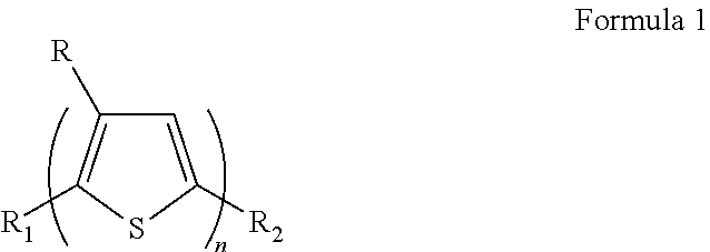
- the polythiophene derivative may be represented by Formula 1 below:
- R is a C7 to C50 alkyl group or a C8 to C50 alkyl group
- R1 and R2 are each independently one of hydrogen, halogen, methyl, and halomethyl
- n is an integer greater than 1 and less than or equal to 40,000, and/or an integer greater than 1 and less than or equal to 10,000.
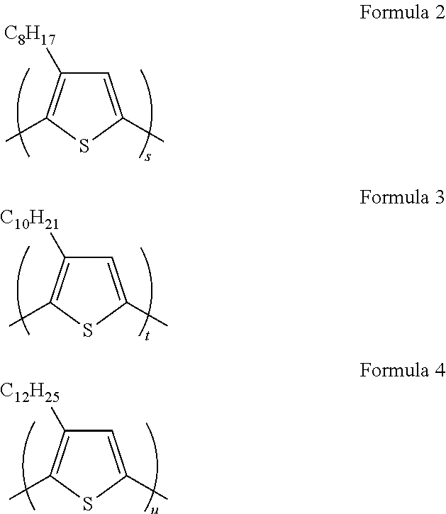
- the polythiophene derivative may be represented by one of Formulae 2, 3, and 4 below:
- s, t, and u are each independently an integer greater than 1 and less than or equal to 40,000.
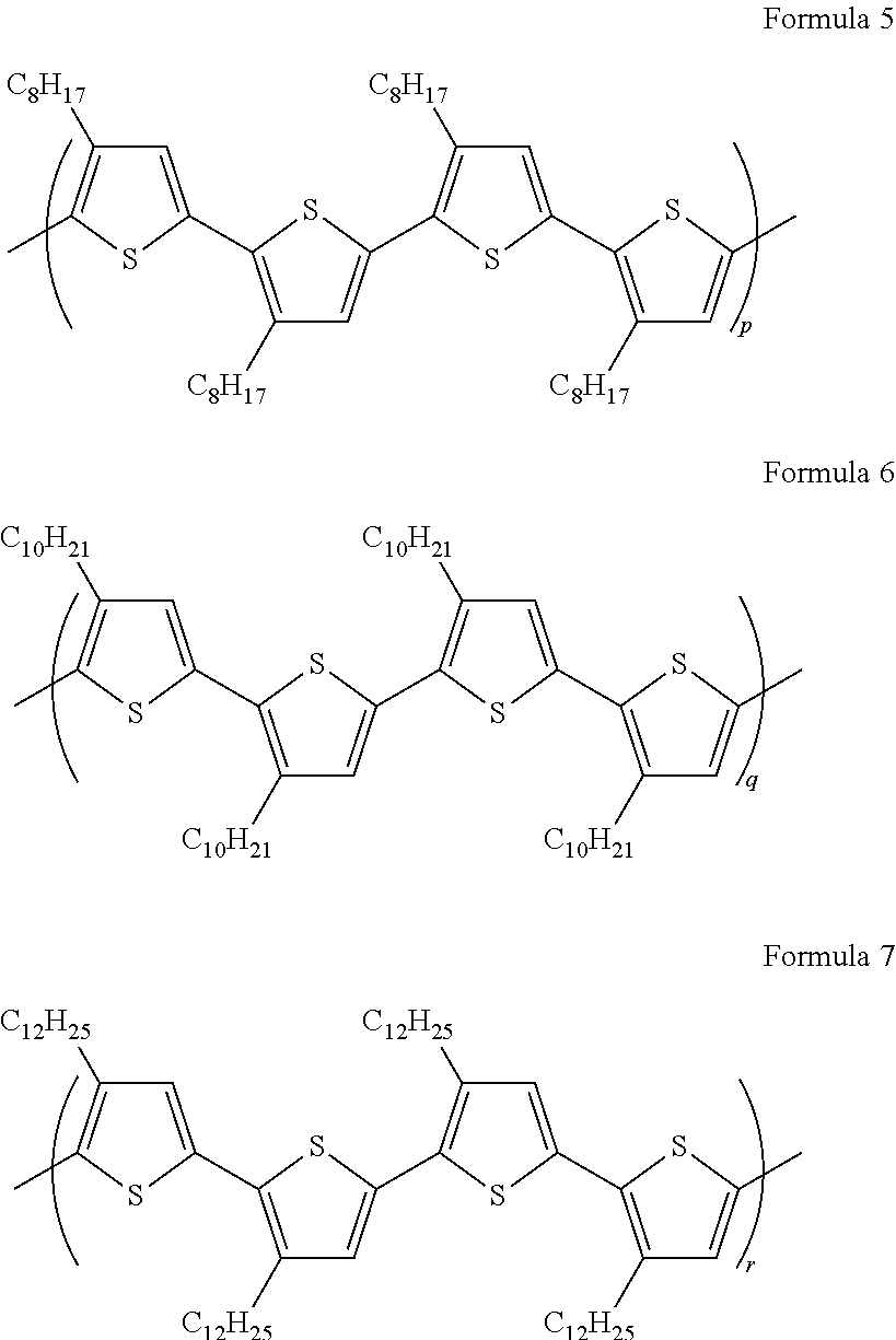
- the polythiophene derivative may be represented by one of Formulae 5, 6, and 7 below:
- p, q, and r are each independently an integer from 1 to 10,000.
- the carbon nanotubes may have a diameter of 3 nm or less.
- the carbon nanotubes may have a diameter of about 0.7 nm to about 3 nm.
- the carbon nanotubes may include single-walled carbon nanotubes, double-walled carbon nanotubes, multi-walled carbon nanotubes, and bundled carbon nanotubes or combinations thereof.
- the solvent may be an organic solvent.
- the carbon nanotubes may have a solubility of less than about 10 mg/L in the organic solvent.
- the organic solvent may include at least one of chloroform, dichloroethane, toluene, xylene, decalin, mesitylene, hexane, and tetrahydrofuran.
- the mixed solution may include a weight ratio of dispersant to carbon nanotubes of about 10:1 to about 1:10.
- An amount of the dispersant in the mixed solution may be from about 0.1 mg/ml to about 1 mg/ml, based on a total volume of the solvent.
- the dispersing the carbon nanotubes in the mixed solution may be performed at a temperature of about ⁇ 40° C. to about 90° C.
- the dispersing the carbon nanotubes in the mixed solution may be performed at a temperature of about ⁇ 20° C. to about 90° C.
- the dispersing the carbon nanotubes in the mixed solution may be performed at a temperature of about 20° C. to about 80° C.
- the dispersing the carbon nanotubes in the mixed solution may be performed at a temperature of about 40° C. to about 70° C.
- the selectively separating the semiconducting carbon nanotubes from the mixed solution may include separating a supernatant containing the dispersed semiconducting carbon nanotubes from the mixed solution by centrifugation.
- An amount of the semiconducting carbon nanotubes in the supernatant may be 75 wt % or greater, based on the total weight of the carbon nanotubes in the supernatant.
- An amount of the semiconducting carbon nanotubes in the supernatant may be 99 wt % or greater, based on the total weight of the carbon nanotubes in the supernatant.
- An amount of the semiconducting carbon nanotubes in the supernatant may be 99.5 wt % or greater, based on the total weight of the carbon nanotubes in the supernatant.
- An amount of the semiconducting carbon nanotubes in the supernatant may be 99.9 wt % or greater of the total carbon nanotubes.
- the carbon nanotubes dispersed in the mixed solution may further include carbon nanotubes having metallic characteristics.
- the method may further include selectively separating the carbon nanotubes having metallic characteristics from the mixed solution.
- an electronic device may include semiconducting carbon nanotubes, and a polythiophene derivative, wherein the polythiophene derivative includes a thiophene ring and a hydrocarbon sidechain linked to the thiophene ring and the hydrocarbon sidechain including an alkyl group containing a carbon number of 7 or greater, and the hydrocarbon sidechain being regioregularly arranged.
- the polythiophene derivative may be represented by Formula 1 below:
- R is a C7 to C50 alkyl group or a C8 to C50 alkyl group
- R1 and R2 are each independently one of hydrogen, halogen, methyl, and halomethyl
- n is an integer greater than 1 and less than or equal to 40,000, and/or an integer greater than 1 and less than or equal to 10,000.
- the polythiophene derivative may be represented by one of Formulae 2, 3, and 4 below:
- s, t, and u are each independently an integer greater than 1 and less than or equal to 40,000.
- the polythiophene derivative may be represented by one of Formulae 5, 6, and 7 below:
- p, q, and r are each independently an integer from 1 to 10,000.
- An amount of the semiconducting carbon nanotubes may be 75 wt % or greater of the total amount of carbon nanotubes.
- An amount of the semiconducting carbon nanotubes may be 99 wt % or greater of the total amount of carbon nanotubes.
- An amount of the semiconducting carbon nanotubes may be 99.5 wt % or greater of the total amount of carbon nanotubes.
- An amount of the semiconducting carbon nanotubes may be 99.9 wt % or greater of the total amount of carbon nanotubes.
- the electronic device may include one of a transistor, a solar cell, a photodetector, a photoconductor, an electrode, and a flexible electronic device.
- the electronic device may include a thin film transistor (TFT), wherein the thin film transistor has a hole mobility of 10 cm 2 /Vs or greater and an on/off current ration of 10 6 or greater.
- TFT thin film transistor
- a dispersion includes a polythiophene derivative and carbon nanotubes, wherein the polythiophene derivative includes: a thiophene ring linked to an alkyl group, the alkyl group containing a carbon number of 7 or greater, and the alkyl group being regioregularly arranged.
- the polythiophene derivative may be represented by Formula 1 below:
- R is a C7 to C50 alkyl group or a C8 to C50 alkyl group
- the polythiophene derivative may be represented by one of Formulae 2, 3, and 4 below:
- s, t, and u are each independently an integer greater than 1 and less than or equal to 40,000.
- the polythiophene derivative may be represented by one of Formulae 5, 6, and 7 below:
- p, q, and r are each independently an integer from 1 to 10,000.
- the dispersion may include semiconducting carbon nanotubes, wherein an amount of the semiconducting carbon nanotubes may be 75 wt % or greater, based on a total weight of the carbon nanotubes.
- An amount of the semiconducting carbon nanotubes may include 99 wt % or greater semiconducting carbon nanotubes.
- An amount of the semiconducting carbon nanotubes may include 99.5 wt % or greater semiconducting carbon nanotubes.
- An amount of the semiconducting carbon nanotubes may include 99.9 wt % or greater semiconducting carbon nanotubes.
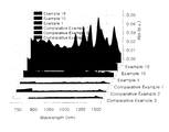
- FIG. 1 is a 3-dimensonal graph of ultraviolet-visible-near infrared (UV-Vis-NIR) absorption spectra of carbon nanotube (CNT) dispersions prepared in Examples 1, 10 and 19, and Comparative Examples 1 to 3;
- UV-Vis-NIR ultraviolet-visible-near infrared
- FIG. 2 is a photograph showing appearances of CNT dispersions prepared in Examples 19;
- FIG. 3 is a 2-dimensional (2D) graph of UV-Vis-NIR absorption spectra of supernatants isolated in Examples 19, and 22 to 27;
- FIG. 4 is a 2D graph of absorbances of the supernatants isolated in Examples 19-27 at 1288 nm;
- FIG. 5 is a graph of Raman spectra of the CNT dispersion of Example 19 before and after centrifugation observed at an excitation energy of 2.33 eV (532 nm);
- FIG. 6 is a graph of Raman spectra of the CNT dispersion of Example 19 before and after centrifugation observed at an excitation energy of 1.96 eV (633 nm);
- FIG. 7 is a graph of Raman spectra of the CNT dispersion of Example 19 before and after centrifugation observed at an excitation energy of 1.58 eV (785 nm);
- FIG. 8A is a schematic view of a thin film transistor (TFT) manufactured using semiconducting CNTs separated from the CNT dispersion prepared in Example 19
- FIG. 8B is a schematic view of a thin film transistor (TFT) according to example embodiments.
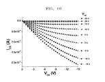
- FIG. 9 is a graph of V GS of a TFT of Example 19 with respect to I DS ;
- FIG. 10 is a graph illustrating output curves of a TFT of Example 19.
- FIGS. 11A and 11B are schematic views of solar cells according to example embodiments.
- Example embodiments will now be described more fully with reference to the accompanying drawings, in which some example embodiments are shown.
- Example embodiments may, however, be embodied in many different forms and should not be construed as being limited to the embodiments set forth herein; rather, these example embodiments are provided so that this disclosure will be thorough and complete, and will fully convey concepts of example embodiments to those of ordinary skill in the art.
- the thicknesses of layers and regions are exaggerated for clarity.
- Like reference numerals in the drawings denote like elements, and thus their description will be omitted.
- Example embodiments are described herein with reference to cross-sectional illustrations that are schematic illustrations of idealized embodiments (and intermediate structures) of example embodiments. As such, variations from the shapes of the illustrations as a result, for example, of manufacturing techniques and/or tolerances, are to be expected. Thus, example embodiments should not be construed as limited to the particular shapes of regions illustrated herein but are to include deviations in shapes that result, for example, from manufacturing.
- a method includes: dispersing CNTs in a mixed solution containing a solvent, the CNTs, and a dispersant, the CNTs including semiconducting CNTs, the dispersant comprising a polythiophene derivative including a thiophene ring and a hydrocarbon sidechain linked to the thiophene ring, wherein the hydrocarbon sidechain includes an alkyl group containing a carbon number of 7 or greater, and the hydrocarbon sidechain being regioregularly arranged, and selectively separating the semiconducting carbon nanotubes from the mixed solution.
- Functions of the polythiophene derivative that enables selective separation of semiconducting CNTs will be explained in more detail. However, this explanation is provided for the purpose of illustration and is not intended to limit the scope of example embodiments.
- a polythiophene derivative is a conjugated polymer having a 7-conjugated structure, in which ⁇ -electrons of a hydrocarbon group of the polythiophene derivative strongly interact with CNTs, i.e., sp 2 carbons of the CNTs, forming ⁇ - ⁇ bonds.
- the polythiophene derivative self-assembles into an interdigitated supramolecular structure of the hydrocarbon sidechain linked to the thiophene ring.
- the hydrocarbon sidechain is regioregularly arranged to form the supramolecular structure with a specific surface arrangement that offers CNTs having specific physical characteristics that improves binding properties of CNTs having specific physical characteristics.
- semiconducting CNTs may be selectively separated with a high yield.
- the polythiophene derivative enables selective separation of semiconducting CNTs with a high yield, without an additional process of separating, for example an insulating surfactant or an insulating polymer, which are used in general methods, from a CNT dispersion.
- regioregular arrangement indicates that substituents in a repeating group including a thiophene ring and the hydrocarbon sidechain linked to the thiophene ring coordinated in a regioregular pattern by being substituted to specific binding sites of the thiophene ring.
- a regiorandom arrangement refers to substituents of the hydrocarbon sidechain that are at random sites of the thiophene ring, resulting in a random arrangement of the hydrocarbon sidechain in diverse directions.
- a steric force of the hydrocarbon sidechain with such a regiorandom arrangement may tilt the hydrocarbon sidechain or thiophene ring, reducing the adsorption of the thiophene ring to CNTs.
- the dispersant used in the method of selectively separating semiconducting CNTs may further include another dispersant, in addition to the polythiophene derivative, as long as it can improve the semiconducting CNT separation efficiency.
- Suitable dispersants include, polysaccharide (dextrin), polyethylenimine (PEI), polyvinylpyrrolidone (PVP), polyethyleneoxide (PEO), and tetraoctylammonium bromide (TOAB). Any suitable dispersant that is commonly used in the art may be used.
- an additive that may improve the separation efficiency may be further used.
- An example of a suitable additive is ethylene diamine tetraacetic acid (EDTA). Any suitable additive that is commonly used in the art for this purpose may be used.
- the dispersant and CNTs may be simultaneously or sequentially added to the solvent, irrespective of the order in which they are added.
- the dispersing of the CNTs in the mixed solution may be performed using a sonicator, blender, or a mixer such as a mechanical mixer, but example embodiments are not limited thereto. Any suitable dispersing method may be used as long as it can prevent and/or substantially limit coagulation of the CNTs.
- the dispersing time may be from about 30 minutes to about 20 hours, or from about 30 minutes to about 10 hours, or from about 30 minutes to about 5 hours, but example embodiments are not limited thereto.
- An applied ultrasonic power may be from about 70% to about 75% of the maximum amplitude.
- the selectively separating of semiconducting CNTs from the mixed solution in which the CNTs are dispersed may be performed by centrifugation.
- the centrifugation may be performed at about 21,000 G to about 25,000 G for about 0.5 hours to about 2 hours.
- the centrifugation may be performed in multiple steps while varying the speed from lower rates to higher rates.
- the centrifugation may be performed at about 13,000 rpm to about 17,000 rpm.
- the polythiophene derivative may include at least ten repeating units.
- the polythiophene derivative including the repeating units as described above may make semiconducting carbon nanotubes wrapping enough to separate semiconducting carbon nanotubes very well
- the hydrocarbon sidechain may have a carbon number of 7 to 50, a carbon number of 7 to 30, and a carbon number of 10 to 30, but example embodiments are not limited thereto.
- the polythiophene derivative may self-assemble to form the supramolecular structure while maintaining flexibility.
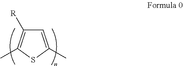
- the polythiophene derivative may be represented by Formula 0 below.
- R may be an alkyl group containing a carbon number of 8 or greater.
- R may be a C8 to C50 alkyl group.
- the polythiophene derivative may be represented by Formula 1 below.
- R is one of a C7-C50 alkyl group, a C8-C50 alkyl group, a C7-C30 alkyl group, a C10-C30 alkyl group, but example embodiments are not limited thereto.
- R 1 and R 2 are each independently any one selected from the group consisting of hydrogen, halogen, alkyl, methyl, halomethyl.
- n is an integer greater than 1 and less than or equal to 40,000, and/or greater than 1 and less than or equal to 10,000.
- the polythiophene derivative may be represented by one of Formulae 2 to 4 below:
- s, t, and u are each independently an integer greater than 1 and less than or equal to 40,000.
- the polythiophene derivative may be represented by one of Formulae 5 to 7 below:
- p, q, and r are each independently an integer from 1 to 10,000.
- the carbon nanotubes may have a diameter of 3 nm or less.
- the carbon nanotubes may have a diameter of about 0.7 nm to about 3 nm, a diameter of about 0.8 nm to about 3 nm, and a diameter of about 0.85 nm to about 3 nm, but example embodiments are not limited thereto.
- the semiconducting carbon nanotubes may have selectivity, and the carbon nanotubes may improve a hole mobility and an on/off current ratio when used in an electronic device such as a thin film transistor.
- the carbon nanotubes in the mixed solution before the semiconducting carbon nanotubes are separated therefrom may include at least one kind of single-walled carbon nanotubes, double-walled carbon nanotubes, and bundled carbon nanotubes.
- the carbon nanotubes in the mixed solution may include any kind of carbon nanotubes used in the art.
- the carbon nanotubes in the mixed solution before the semiconducting carbon nanotubes are separated therefrom may include High-pressure CO (HiPCO) carbon nanotubes.
- HiPCO High-pressure CO
- These carbon nanotubes may be synthesized using electric discharge, thermal decomposition, laser deposition, plasma-enhanced chemical vapor deposition, thermochemical vapor deposition, or electrolysis. However, any suitable method that is commonly used in the art to synthesize carbon nanotubes may be used.
- the solvent in the method of selective separation of the semiconducting carbon nanotubes comprises an organic solvent.
- any suitable solvent that is commonly used in the art may be used.
- the carbon nanotubes may have a solubility of less than about 10 mg/L in the organic solvent, or a solubility of less than about 5 mg/L in the organic solvent, but example embodiments are not limited thereto.
- Suitable organic solvents include: chloroform; dichloroethane; toluene; xylene; decalin; mesitylene; hexane; tetrahydrofuran. These organic solvents may be used individually or in combination of at least two.
- a weight ratio of the dispersant to the carbon nanotubes in the mixed solution may be from about 10:1 to about 1:10, from about 3:1 to about 1:3, and from about 3:1 to about 0.75:1, but example embodiments are not limited thereto.
- the mixing ratio of the dispersant to the carbon nanotubes is within these ranges, the carbon nanotubes may be more effectively dispersed, improving separation yield.
- an additional post-process may not be required for removing, for example, an insulating dispersant.
- An amount of the dispersant in the mixed solution may be from about 0.1 mg/ml to about 1 mg/ml, based on a total volume of the solvent, and from about 0.05 mg/ml to about 1 mg/ml.
- An amount of the carbon nanotubes may be from about 0.01 mg/ml to about 1 mg/ml, based on a total volume of the solvent, and from about 0.005 mg/ml to about 1 mg/ml, but example embodiments are not limited thereto.
- the dispersing of the carbon nanotubes in the mixed solution may be performed at a temperature of about ⁇ 40° C. to about 90° C., and at a temperature of about ⁇ 20° C. to about 90° C.
- the dispersing of the carbon nanotubes in the mixed solution may be performed at a temperature of about 20° C. to about 80° C., and at a temperature of about 40° C. to about 70° C., but example embodiments are not limited thereto.
- the hydrocarbon sidechain of the polythiophene derivative may melt and form the supramolecular structure while maintaining flexibility.
- a steric structure of the polymer backbone may be controlled to have a desired regioregular arrangement that enables selective separation of the semiconducting carbon nanotubes.
- the selectively separating of the semiconducting carbon nanotubes from the mixed solution may include separating a supernatant containing the dispersed semiconducting carbon nanotubes from the mixed solution by centrifugation.
- the supernatant may include only carbon nanotubes that are completely dispersed, excluding undistributed carbon nanotubes in powder or bundles that are precipitated by centrifugation.
- an amount of the semiconducting carbon nanotubes in the supernatant may be 75 wt % or greater, based on the total weight of the carbon nanotubes, and/or 99 wt % or greater of semiconducting carbon nanotubes, and/or 99.5 wt % or greater of semiconducting carbon nanotubes, and/or 99.9 wt % or greater of semiconducting carbon nanotubes.
- a dispersion including metallic carbon nanotubes and semiconducting carbon nanotubes may be centrifuged at about 25,000 G for 2 hours to isolate a supernatant therefrom.
- the rest of the dispersion excluding the supernatant may include 75 wt % or greater of the metallic carbon nanotubes based on the total weight of the residue, and/or 99 wt % or greater of the metallic carbon nanotubes based on the total weight of the residue, and/or 99.5 wt % or greater of the metallic carbon nanotubes based on the total weight of the residue, and and/or 99.9 wt % or greater of the metallic carbon nanotubes.
- metallic carbon nanotubes may also be selectively separated.
- the metallic carbon nanotubes may be used in an electrode and the electrode may be transparent and conductive, but example embodiments are not limited thereto.
- an electronic device includes semiconducting carbon nanotubes, and a polythiophene derivative, wherein the polythiophene derivative includes a thiophene ring and a hydrocarbon sidechain linked to the thiophene ring, the hydrocarbon sidechain including an alkyl group containing a carbon number of 7 or greater, and the hydrocarbon sidechain being regioregularly arranged.
- the semiconducting carbon nanotubes can be used as a charge generation and also as charge transport by the characteristics of the semiconducting carbon nanotubes.
- the polythiophene derivative may self-assemble to form an interdigitated supramolecular structure of the hydrocarbon sidechain linked to the thiophene ring, which is a conjugated polymer structure for selectively dispersing carbon nanotubes.
- the electron device can include selectively separated semiconducting carbon nanotubes with a high yield.
- the polythiophene derivative may be represented by Formula 1 below.
- R is one of a C7-C50 alkyl group, a C8-C50 alkyl group, a C7-C30 alkyl group, a C10-C30 alkyl group, but example embodiments are not limited thereto.
- R 1 and R 2 are each independently one of hydrogen, halogen, alkyl, methyl, halomethyl. Also, n is an integer greater than 1 and less than or equal to 40,000, and/or greater than 1 and less than or equal to 10,000.
- the polythiophene derivative may be represented by one of Formulae 2 to 4 below:
- s, t, and u are each independently an integer greater than 1 and less than or equal to 40,000.
- the polythiophene derivative may be represented by one of Formulae 5 to 7 below:
- p, q, and r are each independently an integer from 1 to 10,000
- an amount of the semiconducting carbon nanotubes may be 75 wt % or greater of the total amount of carbon nanotubes, 99 wt % or greater, 99.5 wt % or greater, and 99.9 wt % or greater, but example embodiments are not limited thereto.
- the electronic device may include a transistor, a solar cell, a photodetector, a photoconductor, an electrode, or a flexible electronic device.
- the electronic device may be a thin film transistor (TFT).
- FIGS. 8A and 8B illustrate thin film transistors (TFTs) according to example embodiments.
- TFTs may include a substrate, a gate electrode, an insulating layer such as a dielectric layer, source and drain electrodes separated from each other, and a semiconductor channel connecting the source and drain electrodes.
- a TFT may include the channel, source and drain electrodes, and insulating layer on the gate electrode, and the gate electrode on the substrate.
- a TFT may include source and drain electrodes on the substrate, a channel connecting the source and drain electrodes, a dielectric layer on the channel, and a gate electrode on the channel layer.
- the substrate may include a material selected from among various non-conductive polymers, such as silicon, glass, fused silica, quartz, plastics, polydimethylsiloxane (PDMS), and combinations thereof, but example embodiments are not limited thereto.
- various non-conductive polymers such as silicon, glass, fused silica, quartz, plastics, polydimethylsiloxane (PDMS), and combinations thereof, but example embodiments are not limited thereto.
- the insulating layer may include an electrically insulating material. Suitable electrically insulating materials include silicon dioxide (SiO 2 ), silicon nitride (Si 3 N 4 ), Teflon, polydimethylmethacrylate, and polymethylmethacrylate (PMMA), but example embodiments are not limited thereto.
- the insulating layer may be disposed under or above the semiconductor channel, or on a side of the semiconductor channel.
- the source and drain electrodes may each include gold (Au), silver (Ag), titanium (Ti), or platinum (Pt), but example embodiments are not limited thereto.
- the semiconductor channel may include high-purity semiconducting carbon nanotubes separated by using the method described above.
- the thin film transistor including the semiconducting carbon nanotubes may have a high hole mobility and a high on/off current ratio, without performing an additional post-process or thermal treatment.
- the thin film transistor may have a hole mobility of 10 cm 2 /Vs or greater, and an on/off current ratio of 10 6 or greater.
- FIG. 9 illustrate a graph of V GS of a TFT of Example 19 with respect to I DS .
- FIG. 10 is a graph illustrating output curves of a TFT of Example 19.
- the hole mobility can be simply described at linear region in FIGS. 9 and 10 as follows:
- ⁇ is a hole mobility and C i is a gate insulator capacitance per unit area
- L, W are the length and width of the channel.
- the C i , L and W come from the thin film transistor. I DS , V GS and V DS are shown in FIGS. 9 and 10 .
- I DS is around zero when V GS is 20V or greater. It means a ‘switched-off’. I DS is decreased when V GS is decreased. In other words, the absolute value of I DS is increased when V GS is decreased. It represents a ‘switched-on’ with a resistance of the thin film transistor.
- the on/off current ratio is a switched-on/switched-off current ratio.
- the on/off current ratio is I DS/on /I DS/off , where V GS/off , V GS/on at a given V DS .
- the I DS/off is I DS at switched-off.
- the I DS/on is I DS at switched-on.
- the V DS/off is V DS at switched-off.
- the V DS/on is V DS at switched-on.
- a carbon nanotube dispersion includes: a polythiophene derivative; and carbon nanotubes, wherein the polythiophene derivative includes a thiophene ring linked to an alkyl group, the alkyl group containing a carbon number of 7 or greater, and the alkyl group being regioregularly arranged.
- the polythiophene derivative may be represented by Formula 1 below.
- R is one of a C7-C50 alkyl group, a C8-C50 alkyl group, a C7-C30 alkyl group, a C10-C30 alkyl group, but example embodiments are not limited thereto.
- R 1 and R 2 are each independently one of hydrogen, halogen, alkyl, methyl, halomethyl. Also, n is an integer greater than 1 and less than or equal to 40,000, and/or greater than 1 and less than or equal to 10,000.
- the polythiophene derivative may be represented by one of Formulae 2 to 4 below:
- s, t, and u are each independently an integer greater than 1 and less than or equal 40,000.
- semiconducting carbon nanotubes may be selectively separated using an amount of such a dispersant.
- the polythiophene derivative may be represented by one of Formulae 5 to 7 below:
- An amount of the semiconducting carbon nanotubes may be 75 wt % or greater of the total amount of carbon nanotubes.
- An amount of the semiconducting carbon nanotubes may be 99 wt % or greater, 99.5 wt % or greater, and 99.9 wt % or greater of the total amount of carbon nanotubes.
- the dispersion including semiconducting carbon nanotubes may include only semiconducting carbon nanotubes with 100% and/or about 100% purity.
- the polythiophene derivative may be synthesized using a McCullough method or a Rieke method. However, any suitable method that is commonly used in the art may be used to synthesize the polythiophene derivative.
- the resulting dispersion was centrifuged at about 25,000 G for 2 hours to isolate a supernatant, which was used as a carbon nanotube dispersion including semiconducting single-walled carbon nanotubes.
- a carbon nanotube dispersion including semiconducting single-walled carbon nanotubes was prepared in the same manner as in Example 1, except that the single-walled carbon nanotubes were dispersed at ⁇ 40° C.
- a carbon nanotube dispersion including semiconducting single-walled carbon nanotubes was prepared in the same manner as in Example 1, except that the single-walled carbon nanotubes were dispersed at ⁇ 30° C.
- a carbon nanotube dispersion including semiconducting single-walled carbon nanotubes was prepared in the same manner as in Example 1, except that the single-walled carbon nanotubes were dispersed at 15° C.
- a carbon nanotube dispersion including semiconducting single-walled carbon nanotubes was prepared in the same manner as in Example 1, except that the single-walled carbon nanotubes were dispersed at 20° C.
- a carbon nanotube dispersion including semiconducting single-walled carbon nanotubes was prepared in the same manner as in Example 1, except that the single-walled carbon nanotubes were dispersed at 40° C.
- a carbon nanotube dispersion including semiconducting single-walled carbon nanotubes was prepared in the same manner as in Example 1, except that the single-walled carbon nanotubes were dispersed at 60° C.
- a carbon nanotube dispersion including semiconducting single-walled carbon nanotubes was prepared in the same manner as in Example 1, except that the single-walled carbon nanotubes were dispersed at 70° C.
- a carbon nanotube dispersion including semiconducting single-walled carbon nanotubes was prepared in the same manner as in Example 1, except that the single-walled carbon nanotubes were dispersed at 90° C.
- a carbon nanotube dispersion including semiconducting single-walled carbon nanotubes was prepared in the same manner as in Example 1, except that a regioregular poly(3-decyl)thiophene (available from Sigma-Aldrich Co.) dispersant was used to obtain a dispersion including metallic single-walled carbon nanotubes and semiconducting single-walled carbon nanotubes, which was then centrifuged to obtain the carbon nanotube dispersion including semiconducting single-walled carbon nanotubes.
- a regioregular poly(3-decyl)thiophene available from Sigma-Aldrich Co.
- a carbon nanotube dispersion including semiconducting single-walled carbon nanotubes was prepared in the same manner as in Example 10, except that the single-walled carbon nanotubes were dispersed at ⁇ 40° C.
- a carbon nanotube dispersion including semiconducting single-walled carbon nanotubes was prepared in the same manner as in Example 10, except that the single-walled carbon nanotubes were dispersed at ⁇ 30° C.
- a carbon nanotube dispersion including semiconducting single-walled carbon nanotubes was prepared in the same manner as in Example 10, except that the single-walled carbon nanotubes were dispersed at 15° C.
- a carbon nanotube dispersion including semiconducting single-walled carbon nanotubes was prepared in the same manner as in Example 10, except that the single-walled carbon nanotubes were dispersed at 20° C.
- a carbon nanotube dispersion including semiconducting single-walled carbon nanotubes was prepared in the same manner as in Example 10, except that the single-walled carbon nanotubes were dispersed at 40° C.
- a carbon nanotube dispersion including semiconducting single-walled carbon nanotubes was prepared in the same manner as in Example 10, except that the single-walled carbon nanotubes were dispersed at 60° C.
- a carbon nanotube dispersion including semiconducting single-walled carbon nanotubes was prepared in the same manner as in Example 10, except that the single-walled carbon nanotubes were dispersed at 70° C.
- a carbon nanotube dispersion including semiconducting single-walled carbon nanotubes was prepared in the same manner as in Example 10, except that the single-walled carbon nanotubes were dispersed at 90° C.
- a carbon nanotube dispersion including semiconducting single-walled carbon nanotubes was prepared in the same manner as in Example 1, except that a regioregular poly(3-dodecyl)thiophene (available from Sigma-Aldrich Co.) dispersant was used to obtain a dispersion including metallic single-walled carbon nanotubes and semiconducting single-walled carbon nanotubes, which was then centrifuged to obtain the carbon nanotube dispersion including semiconducting single-walled carbon nanotubes.
- a regioregular poly(3-dodecyl)thiophene available from Sigma-Aldrich Co.
- a carbon nanotube dispersion including semiconducting single-walled carbon nanotubes was prepared in the same manner as in Example 19, except that the single-walled carbon nanotubes were dispersed at ⁇ 40° C.
- a carbon nanotube dispersion including semiconducting single-walled carbon nanotubes was prepared in the same manner as in Example 19, except that the single-walled carbon nanotubes were dispersed at ⁇ 30° C.
- a carbon nanotube dispersion including semiconducting single-walled carbon nanotubes was prepared in the same manner as in Example 19, except that the single-walled carbon nanotubes were dispersed at 15° C.
- a carbon nanotube dispersion including semiconducting single-walled carbon nanotubes was prepared in the same manner as in Example 19, except that the single-walled carbon nanotubes were dispersed at 20° C.
- a carbon nanotube dispersion including semiconducting single-walled carbon nanotubes was prepared in the same manner as in Example 19, except that the single-walled carbon nanotubes were dispersed at 40° C.
- a carbon nanotube dispersion including semiconducting single-walled carbon nanotubes was prepared in the same manner as in Example 19, except that the single-walled carbon nanotubes were dispersed at 60° C.
- a carbon nanotube dispersion including semiconducting single-walled carbon nanotubes was prepared in the same manner as in Example 19, except that the single-walled carbon nanotubes were dispersed at 70° C.
- a carbon nanotube dispersion including semiconducting single-walled carbon nanotubes was prepared in the same manner as in Example 19, except that the single-walled carbon nanotubes were dispersed at 90° C.
- a carbon nanotube dispersion including semiconducting single-walled carbon nanotubes was prepared in the same manner as in Example 1, except that a regioregular poly(3-hexyl)thiophene (available from Sigma-Aldrich Co.) dispersant was used to obtain a dispersion including metallic single-walled carbon nanotubes and semiconducting single-walled carbon nanotubes, which was then centrifuged to obtain the carbon nanotube dispersion including semiconducting single-walled carbon nanotubes.
- a regioregular poly(3-hexyl)thiophene available from Sigma-Aldrich Co.
- a carbon nanotube dispersion including semiconducting single-walled carbon nanotubes was prepared in the same manner as in Example 1, except that a poly(3,3′′′-didodecyl-quarter-thiophene)(available from Sigma-Aldrich Co.) dispersant represented by Formula 8 below was used to obtain a dispersion including metallic single-walled carbon nanotubes and semiconducting single-walled carbon nanotubes, which was then centrifuged to obtain the carbon nanotube dispersion including semiconducting single-walled carbon nanotubes.
- a poly(3,3′′′-didodecyl-quarter-thiophene)(available from Sigma-Aldrich Co.) dispersant represented by Formula 8 below was used to obtain a dispersion including metallic single-walled carbon nanotubes and semiconducting single-walled carbon nanotubes, which was then centrifuged to obtain the carbon nanotube dispersion including semiconducting single-walled carbon nanotubes.
- n is an integer from 50 to 500.
- a carbon nanotube dispersion including semiconducting single-walled carbon nanotubes was prepared in the same manner as in Example 1, except that a regioregular poly(3-methyl-4-decyl-thiophene-2,5-diyl)(available from Sigma-Aldrich Co.) dispersant represented by Formula 9 below was used to obtain a dispersion including metallic single-walled carbon nanotubes and semiconducting single-walled carbon nanotubes, which was then centrifuged to obtain the carbon nanotube dispersion including semiconducting single-walled carbon nanotubes.
- a regioregular poly(3-methyl-4-decyl-thiophene-2,5-diyl)(available from Sigma-Aldrich Co.) dispersant represented by Formula 9 below was used to obtain a dispersion including metallic single-walled carbon nanotubes and semiconducting single-walled carbon nanotubes, which was then centrifuged to obtain the carbon nanotube dispersion including semi
- n is an integer from 50 to 500.
- the CNT dispersions of Examples 1, 10 and 19 show stronger absorption peak intensities in a near infrared (NIR) range of 750 nm to 1500 nm, than those of Comparative Examples 1 to 3, indicating that the CNT dispersions of Examples 1, 10 and 19 include remarkably larger amounts of semiconducting CNTs.
- NIR near infrared
- the semiconductor dispersions of Examples 19-27 prepared via the dispersing of the mixed solutions of the polythiophene derivatives, the CNTs, and the solvents at a temperature of ⁇ 40° C. to 90° C. include large amounts of semiconducting CNTs.
- FIG. 3 is a 2-dimensional (2D) graph of UV-Vis-NIR absorption spectra of supernatants isolated in Examples 19, and 22 to 27.
- FIG. 4 is a 2D graph of absorbances of the supernatants isolated in Examples 19-27 at 1288 nm.
- Raman spectra in a radial breathing mode (RBM) of the CNT dispersion of Example 19 before centrifugation and a supernatant thereof obtained after the centrifugation at 25,000 G for 2 hours were observed using a Raman spectrometer (T.Y. Horriba) at different excitation energies of 2.33 eV (532 nm), 1.94 eV (633 nm), and 1.59 eV (785 nm). The results are shown in FIGS. 5 to 7 .
- FIG. 5 which illustrates RBM spectra in a region of 180 cm ⁇ 1 to 285 cm ⁇ 1 when excited at 2.33 eV (532 nm)
- resonance peaks of metallic single-walled CNTs appear in the dispersion before centrifugation.
- the resonance peaks of metallic CNTs disappear in the supernatant isolated from the dispersion by centrifugation.
- FIG. 6 which illustrates RBM spectra in a region of 180 cm ⁇ 1 to 285 cm ⁇ 1 when excited at 1.94 eV (633 nm)
- resonance peaks of metallic CNTs and semiconducting CNTs appear in the dispersion before centrifugation, whereas the resonance peaks of metallic CNTs disappear in the supernatant isolated from the dispersion by centrifugation.
- the resonance peaks of semiconducting CNTs mostly remain in a region of 240 cm ⁇ 1 to 285 cm ⁇ 1 in which resonance peaks of nonmetallic CNTs normally appear.
- FIG. 7 which illustrates RBM spectra in a region of 180 cm ⁇ 1 to 285 cm ⁇ 1 when excited at 1.59 eV (785 nm)
- resonance peaks of only semiconducting CNTs appear in the dispersion before centrifugation, whereas the resonance peaks of semiconducting CNTs remain in the supernatant isolated from the dispersion by centrifugation.
- the supernatant obtained after centrifugation include semiconducting single-walled CNTs with a high yield such as about 100%, excluding the metallic CNTs, which were almost completely removed from the supernatant by the centrifugation.
- a TFT was manufactured with a Pt source electrode, a Ti drain electrode, and a gate electrode (heavily n-doped Si substrate), and a SiO 2 dielectric layer (having a thickness of 300 nm).
- a surface of the SiO 2 insulating layer was modified to have a self-assembled monolayer (SAM) including an amine terminal group.
- SAM self-assembled monolayer
- CNTs which were randomly disposed between the source electrode and the drain electrode, had an average length of 1.0 ⁇ m ⁇ 0.1 ⁇ m, as observed by scanning electron microscopy (SEM). The CNTs were used to form a channel between the source electrode and the drain electrode.
- the CNT channel included less than fifty (>50) CNTs per mm 2 on average, and had a thickness of about 2.3 nm.
- the TFT is found to have a hole mobility of 10 cm 2 /Vs or greater, and an on/off current ratio of 10 6 or greater.
- a method of selective separation of semiconducting CNTs enables semiconducting CNTs to be separated easily with a high yield, and an electronic device including semiconducting CNTs separated by using the method may have improved electrical characteristics.
- FIGS. 11A and 11B are schematic views of solar cells according to example embodiments.
- a solar cell 100 may include a substrate 10 , lower electrode 20 , photoactive layer 50 , and an upper electrode 60 sequentially stacked.
- the material of the substrate 10 may include one of non-conductive polymers, silicon, glass, fused silica, quartz, plastics, polydimethylsiloxane (PDMS), and combinations thereof, but example embodiments are not limited thereto.
- the lower electrode 20 and upper electrode 60 each may include at least one transparent conductive oxide material, such as zinc oxide, tin oxide, indium tin oxide, and the like, but example embodiments are not limited thereto.
- the material and/or materials of the lower electrode 20 and the upper electrode 60 may be the same or different.
- the photoactive layer 50 includes a n-type layer 30 and a p-type layer 40 .
- the p-type layer 40 may include a dispersion containing semiconducting carbon nanotubes according to example embodiments.
- the semiconducting CNTs may be used as a charge generation in solar cells. Further, the semiconducting CNTs may be used to facilitate a charge transport, according to the characteristics of the CNTs.
- the polythiophene derivative can be used as an electron donor.
- a solar cell 200 may be similar to the solar cell 100 in FIG. 11A , except the photoactive layer 90 includes a mixture of p-type material 80 and n-type material 70 .
- the discussion of like structural elements between solar cells 100 and 200 will be omitted.
- the p-type layer 80 may include a dispersion containing semiconducting carbon nanotubes according to example embodiments.
Landscapes
- Chemical & Material Sciences (AREA)
- Engineering & Computer Science (AREA)
- Nanotechnology (AREA)
- Materials Engineering (AREA)
- Organic Chemistry (AREA)
- Physics & Mathematics (AREA)
- Crystallography & Structural Chemistry (AREA)
- Inorganic Chemistry (AREA)
- Manufacturing & Machinery (AREA)
- Condensed Matter Physics & Semiconductors (AREA)
- General Physics & Mathematics (AREA)
- Spectroscopy & Molecular Physics (AREA)
- Medicinal Chemistry (AREA)
- Health & Medical Sciences (AREA)
- Chemical Kinetics & Catalysis (AREA)
- Polymers & Plastics (AREA)
- Dispersion Chemistry (AREA)
- Theoretical Computer Science (AREA)
- Mathematical Physics (AREA)
- Composite Materials (AREA)
- Carbon And Carbon Compounds (AREA)
- Thin Film Transistor (AREA)
- Emulsifying, Dispersing, Foam-Producing Or Wetting Agents (AREA)
- Electrodes Of Semiconductors (AREA)
Abstract
Description


-
- R1 and R2 are each independently one of hydrogen, halogen, methyl, and halomethyl; and
- n is an integer greater than 1 and less than or equal to 40,000, and/or an integer greater than 1 and less than or equal to 10,000.
- R1 and R2 are each independently one of hydrogen, halogen, methyl, and halomethyl; and


wherein p, q, and r are each independently an integer from 1 to 10,000.

In

wherein s, t, and u are each independently an integer greater than 1 and less than or equal to 40,000.
wherein p, q, and r are each independently an integer from 1 to 10,000.
wherein s, t, and u are each independently an integer greater than 1 and less than or equal to 40,000.

wherein p, q, and r are each independently an integer from 1 to 10,000
where μ is a hole mobility and Ci is a gate insulator capacitance per unit area, and L, W are the length and width of the channel. The Ci, L and W come from the thin film transistor. IDS, VGS and VDS are shown in


wherein s, t, and u are each independently an integer greater than 1 and less than or equal 40,000.

wherein p, q, and r are each independently an integer from 1 to 10,000. When the numbers of the repeating units of the polythiophene derivatives are within the foregoing range, semiconducting carbon nanotubes may be selectively separated using an amount of such a dispersant.

wherein m is an integer from 50 to 500.

wherein n is an integer from 50 to 500.
Claims (28)


Priority Applications (6)
| Application Number | Priority Date | Filing Date | Title |
|---|---|---|---|
| US13/282,783 US9502152B2 (en) | 2010-11-01 | 2011-10-27 | Method of selective separation of semiconducting carbon nanotubes, dispersion of semiconducting carbon nanotubes, and electronic device including carbon nanotubes separated by using the method |
| PCT/KR2011/008236 WO2012060601A2 (en) | 2010-11-01 | 2011-11-01 | Method of selective separation of semiconducting carbon nanotubes, dispersion of semiconducting carbon nanotubes, and electronic device including carbon nanotubes separated by using the method |
| EP11838206.8A EP2635524B1 (en) | 2010-11-01 | 2011-11-01 | Method of selective separation of semiconducting carbon nanotubes |
| JP2013536538A JP5719447B2 (en) | 2010-11-01 | 2011-11-01 | Method for selectively separating semiconducting carbon nanotubes, dispersion of semiconducting carbon nanotubes, and electronic device including carbon nanotubes separated by the method |
| KR1020137007233A KR101910984B1 (en) | 2010-11-01 | 2011-11-01 | Method of selective separation of semiconducting carbon nanotubes, dispersion of semiconducting carbon nanotubes, and electronic device including carbon nanotubes separated by using the method |
| US15/290,568 US10355216B2 (en) | 2010-11-01 | 2016-10-11 | Method of selective separation of semiconducting carbon nanotubes, dispersion of semiconducting carbon nanotubes, and electronic device including carbon nanotubes separated by using the method |
Applications Claiming Priority (2)
| Application Number | Priority Date | Filing Date | Title |
|---|---|---|---|
| US40880510P | 2010-11-01 | 2010-11-01 | |
| US13/282,783 US9502152B2 (en) | 2010-11-01 | 2011-10-27 | Method of selective separation of semiconducting carbon nanotubes, dispersion of semiconducting carbon nanotubes, and electronic device including carbon nanotubes separated by using the method |
Related Child Applications (1)
| Application Number | Title | Priority Date | Filing Date |
|---|---|---|---|
| US15/290,568 Division US10355216B2 (en) | 2010-11-01 | 2016-10-11 | Method of selective separation of semiconducting carbon nanotubes, dispersion of semiconducting carbon nanotubes, and electronic device including carbon nanotubes separated by using the method |
Publications (2)
| Publication Number | Publication Date |
|---|---|
| US20120104328A1 US20120104328A1 (en) | 2012-05-03 |
| US9502152B2 true US9502152B2 (en) | 2016-11-22 |
Family
ID=45995642
Family Applications (2)
| Application Number | Title | Priority Date | Filing Date |
|---|---|---|---|
| US13/282,783 Active 2035-09-03 US9502152B2 (en) | 2010-11-01 | 2011-10-27 | Method of selective separation of semiconducting carbon nanotubes, dispersion of semiconducting carbon nanotubes, and electronic device including carbon nanotubes separated by using the method |
| US15/290,568 Active US10355216B2 (en) | 2010-11-01 | 2016-10-11 | Method of selective separation of semiconducting carbon nanotubes, dispersion of semiconducting carbon nanotubes, and electronic device including carbon nanotubes separated by using the method |
Family Applications After (1)
| Application Number | Title | Priority Date | Filing Date |
|---|---|---|---|
| US15/290,568 Active US10355216B2 (en) | 2010-11-01 | 2016-10-11 | Method of selective separation of semiconducting carbon nanotubes, dispersion of semiconducting carbon nanotubes, and electronic device including carbon nanotubes separated by using the method |
Country Status (5)
| Country | Link |
|---|---|
| US (2) | US9502152B2 (en) |
| EP (1) | EP2635524B1 (en) |
| JP (1) | JP5719447B2 (en) |
| KR (1) | KR101910984B1 (en) |
| WO (1) | WO2012060601A2 (en) |
Cited By (3)
| Publication number | Priority date | Publication date | Assignee | Title |
|---|---|---|---|---|
| US20170222151A1 (en) * | 2016-01-29 | 2017-08-03 | University Of Kentucky Research Foundation | Water processable n-type organic semiconductor |
| US20190010342A1 (en) * | 2016-01-08 | 2019-01-10 | National Research Council Of Canada | Hydrophylic semiconducting single-walled carbon nanotube inks |
| US10355216B2 (en) * | 2010-11-01 | 2019-07-16 | Samsung Electronics Co., Ltd. | Method of selective separation of semiconducting carbon nanotubes, dispersion of semiconducting carbon nanotubes, and electronic device including carbon nanotubes separated by using the method |
Families Citing this family (31)
| Publication number | Priority date | Publication date | Assignee | Title |
|---|---|---|---|---|
| KR100902509B1 (en) * | 2007-05-29 | 2009-06-15 | 삼성전자주식회사 | Selective separation method of carbon nanotubes, electrode comprising carbon nanotubes separated by the above method and oligomer dispersant for carbon nanotubes |
| US9525135B2 (en) * | 2013-01-28 | 2016-12-20 | Xerox Corporation | Thixotropic composition |
| CN103236442B (en) * | 2013-04-23 | 2016-12-28 | 京东方科技集团股份有限公司 | Thin film transistor (TFT) and manufacture method, array base palte, electronic installation |
| CN105611986B (en) * | 2013-08-20 | 2018-05-11 | 加拿大国家研究委员会 | Method for purifying semiconductor single-walled carbon |
| JP6300300B2 (en) * | 2013-11-12 | 2018-03-28 | 国立研究開発法人産業技術総合研究所 | Field effect transistor using carbon nanotube aggregates |
| US9455421B2 (en) | 2013-11-21 | 2016-09-27 | Atom Nanoelectronics, Inc. | Devices, structures, materials and methods for vertical light emitting transistors and light emitting displays |
| KR20160006465A (en) | 2014-07-09 | 2016-01-19 | 이사욱 | Method for processing coupon and coupon processing system |
| CN106804109B (en) * | 2014-08-12 | 2020-01-07 | 巴斯夫欧洲公司 | Sorting of carbon nanotubes |
| US10395804B2 (en) | 2015-03-24 | 2019-08-27 | The Board Of Trustees Of The Leland Stanford Junior University | Isolating semiconducting single-walled nanotubes or metallic single-walled nanotubes and approaches therefor |
| KR101775782B1 (en) | 2015-08-31 | 2017-09-11 | 국방과학연구소 | Method for removing covalent functional groups attached on single-walled carbon nanotubes |
| KR102539449B1 (en) * | 2015-11-27 | 2023-06-02 | 더 보드 어브 트러스티스 어브 더 리랜드 스탠포드 주니어 유니버시티 | degradable conjugated polymer |
| US10957868B2 (en) | 2015-12-01 | 2021-03-23 | Atom H2O, Llc | Electron injection based vertical light emitting transistors and methods of making |
| US10541374B2 (en) * | 2016-01-04 | 2020-01-21 | Carbon Nanotube Technologies, Llc | Electronically pure single chirality semiconducting single-walled carbon nanotube for large scale electronic devices |
| CN108023016B (en) * | 2016-10-31 | 2020-07-10 | 清华大学 | Preparation method of thin film transistor |
| US10847757B2 (en) | 2017-05-04 | 2020-11-24 | Carbon Nanotube Technologies, Llc | Carbon enabled vertical organic light emitting transistors |
| US10665796B2 (en) | 2017-05-08 | 2020-05-26 | Carbon Nanotube Technologies, Llc | Manufacturing of carbon nanotube thin film transistor backplanes and display integration thereof |
| US10978640B2 (en) | 2017-05-08 | 2021-04-13 | Atom H2O, Llc | Manufacturing of carbon nanotube thin film transistor backplanes and display integration thereof |
| US10640381B2 (en) | 2017-06-09 | 2020-05-05 | National Research Council Of Canada | Method for polymer removal from single-walled carbon nanotubes |
| KR102113219B1 (en) * | 2017-10-25 | 2020-05-21 | 광주과학기술원 | Conjugated molecule for selective separation of carbon nanotubes |
| KR102160329B1 (en) * | 2017-12-28 | 2020-09-28 | 동국대학교 산학협력단 | Thin film transistor comprising double semiconductor |
| JP7014675B2 (en) | 2018-05-23 | 2022-02-01 | 花王株式会社 | Method for manufacturing semiconductor type single-walled carbon nanotube dispersion liquid |
| CN108987576B (en) * | 2018-07-18 | 2020-12-25 | 深圳市华星光电半导体显示技术有限公司 | Preparation method of carbon nanotube composite film, carbon nanotube TFT and preparation method thereof |
| CN110902670B (en) * | 2018-09-14 | 2021-07-20 | 中国科学院苏州纳米技术与纳米仿生研究所 | A kind of carbon nanotube oriented film, its preparation method and application |
| KR20210134616A (en) | 2019-01-04 | 2021-11-10 | 아톰 에이치투오, 엘엘씨 | Carbon nanotube-based radio frequency device |
| KR102234345B1 (en) * | 2019-02-18 | 2021-03-31 | 가천대학교 산학협력단 | Scalable separation of semiconducting single walled carbon nanotubes using bath sonication |
| JP7002517B2 (en) | 2019-11-15 | 2022-01-20 | 花王株式会社 | Method for manufacturing semiconductor type single-walled carbon nanotube dispersion liquid |
| JP6900453B2 (en) | 2019-11-15 | 2021-07-07 | 花王株式会社 | Method for manufacturing semiconductor type single-walled carbon nanotube dispersion liquid |
| GB2592891B (en) | 2019-12-19 | 2022-06-15 | Univ Of The West Of England Bristol | Low-power contactless physiological sensor |
| CN113120882B (en) * | 2020-01-15 | 2022-10-18 | 清华大学 | Method for obtaining metallic carbon nanotubes |
| US20230227314A1 (en) * | 2020-05-14 | 2023-07-20 | Nano-C, Inc. | Carbon nanostructure compositions and methods for purification thereof |
| CN112812507B (en) * | 2021-01-07 | 2021-11-16 | 江南大学 | A single chiral carbon nanotube-thiophene polymer composite material and preparation method thereof |
Citations (14)
| Publication number | Priority date | Publication date | Assignee | Title |
|---|---|---|---|---|
| KR20050077542A (en) | 2004-01-28 | 2005-08-03 | 삼성에스디아이 주식회사 | A fabric solar cell and a method for preparing the same |
| US20060045838A1 (en) | 2004-08-24 | 2006-03-02 | General Electric Company | Nanotubes and methods of dispersing and separating nanotubes |
| JP2006265035A (en) | 2005-03-24 | 2006-10-05 | National Institute Of Advanced Industrial & Technology | CARBON NANOTUBE-CONTAINING THIN FILM, METHOD FOR PRODUCING THE THIN FILM, PHOTOELECTRIC CONVERSION MATERIAL, PHOTOELECTRIC CONVERSION ELEMENT, ELECTROLUMINESCENT MATERIAL, AND ELECTROLUMINESCENT ELEMENT WITH THE SAME |
| JP2007031238A (en) | 2005-07-29 | 2007-02-08 | Sony Corp | Method for separating metallic carbon nanotube, method for producing semiconducting carbon nanotube thin film, thin film transistor, method for producing the same, electronic device and method for producing the same |
| KR20070042179A (en) | 2004-07-16 | 2007-04-20 | 더 트러스티즈 오브 프린스턴 유니버시티 | Organic device with fiber structure |
| US7226818B2 (en) | 2004-10-15 | 2007-06-05 | General Electric Company | High performance field effect transistors comprising carbon nanotubes fabricated using solution based processing |
| US20080066802A1 (en) | 2006-03-23 | 2008-03-20 | Solexant Corp. | Photovoltaic device containing nanoparticle sensitized carbon nanotubes |
| JP2008238162A (en) | 2007-02-27 | 2008-10-09 | Samsung Electronics Co Ltd | Dispersant for carbon nanotube and carbon nanotube composition containing the same |
| US20090020732A1 (en) * | 2007-05-29 | 2009-01-22 | Samsung Electronics Co., Ltd. | Method of selectively separating carbon nanotubes, electrode comprising metallic carbon nanotubes separated by the method and oligomer dispersant for selectively separating carbon nanotubes |
| US7488876B2 (en) | 2004-05-12 | 2009-02-10 | Samsung Corning Precision Glass Co., Ltd. | Method for selectively separating semiconductive carbon nanotubes |
| US20090085012A1 (en) * | 2007-09-27 | 2009-04-02 | Christos Chochos | Multifunctional materials consisting of regioregular poly(3-alkylthiophene)s covalently attached on carbon nanotubes for photovoltaic applications |
| US7514063B1 (en) | 2008-02-08 | 2009-04-07 | International Business Machines Corporation | Method for the purification of semiconducting single walled carbon nanotubes |
| US20090232724A1 (en) | 2008-03-11 | 2009-09-17 | Ali Afzali-Ardakani | Method of separating metallic and semiconducting carbon nanotubes from a mixture of same |
| US20150107638A1 (en) * | 2012-07-11 | 2015-04-23 | Fujifilm Corporation | Thermoelectric conversion element and thermoelectric conversion material |
Family Cites Families (3)
| Publication number | Priority date | Publication date | Assignee | Title |
|---|---|---|---|---|
| KR20070098433A (en) | 2006-03-30 | 2007-10-05 | 삼성전자주식회사 | Screening method of semiconducting carbon nanotubes |
| US8455297B1 (en) * | 2010-07-07 | 2013-06-04 | International Business Machines Corporation | Method to fabricate high performance carbon nanotube transistor integrated circuits by three-dimensional integration technology |
| US9502152B2 (en) * | 2010-11-01 | 2016-11-22 | Samsung Electronics Co., Ltd. | Method of selective separation of semiconducting carbon nanotubes, dispersion of semiconducting carbon nanotubes, and electronic device including carbon nanotubes separated by using the method |
-
2011
- 2011-10-27 US US13/282,783 patent/US9502152B2/en active Active
- 2011-11-01 JP JP2013536538A patent/JP5719447B2/en active Active
- 2011-11-01 WO PCT/KR2011/008236 patent/WO2012060601A2/en not_active Ceased
- 2011-11-01 EP EP11838206.8A patent/EP2635524B1/en active Active
- 2011-11-01 KR KR1020137007233A patent/KR101910984B1/en active Active
-
2016
- 2016-10-11 US US15/290,568 patent/US10355216B2/en active Active
Patent Citations (18)
| Publication number | Priority date | Publication date | Assignee | Title |
|---|---|---|---|---|
| KR20050077542A (en) | 2004-01-28 | 2005-08-03 | 삼성에스디아이 주식회사 | A fabric solar cell and a method for preparing the same |
| US7638706B2 (en) | 2004-01-28 | 2009-12-29 | Samsung Sdi Co., Ltd. | Fibril solar cell and method of manufacture |
| US7488876B2 (en) | 2004-05-12 | 2009-02-10 | Samsung Corning Precision Glass Co., Ltd. | Method for selectively separating semiconductive carbon nanotubes |
| US7561772B2 (en) | 2004-07-16 | 2009-07-14 | The Trustees Of Princeton University | Organic devices having a fiber structure |
| KR20070042179A (en) | 2004-07-16 | 2007-04-20 | 더 트러스티즈 오브 프린스턴 유니버시티 | Organic device with fiber structure |
| US20060045838A1 (en) | 2004-08-24 | 2006-03-02 | General Electric Company | Nanotubes and methods of dispersing and separating nanotubes |
| US7247670B2 (en) | 2004-08-24 | 2007-07-24 | General Electric Company | Nanotubes and methods of dispersing and separating nanotubes |
| US7226818B2 (en) | 2004-10-15 | 2007-06-05 | General Electric Company | High performance field effect transistors comprising carbon nanotubes fabricated using solution based processing |
| JP2006265035A (en) | 2005-03-24 | 2006-10-05 | National Institute Of Advanced Industrial & Technology | CARBON NANOTUBE-CONTAINING THIN FILM, METHOD FOR PRODUCING THE THIN FILM, PHOTOELECTRIC CONVERSION MATERIAL, PHOTOELECTRIC CONVERSION ELEMENT, ELECTROLUMINESCENT MATERIAL, AND ELECTROLUMINESCENT ELEMENT WITH THE SAME |
| JP2007031238A (en) | 2005-07-29 | 2007-02-08 | Sony Corp | Method for separating metallic carbon nanotube, method for producing semiconducting carbon nanotube thin film, thin film transistor, method for producing the same, electronic device and method for producing the same |
| US20080066802A1 (en) | 2006-03-23 | 2008-03-20 | Solexant Corp. | Photovoltaic device containing nanoparticle sensitized carbon nanotubes |
| KR20080111488A (en) | 2006-03-23 | 2008-12-23 | 솔렉슨트 코포레이션 | Photovoltaic Devices Containing Nanoparticle-Sensitive Carbon Nanotubes |
| JP2008238162A (en) | 2007-02-27 | 2008-10-09 | Samsung Electronics Co Ltd | Dispersant for carbon nanotube and carbon nanotube composition containing the same |
| US20090020732A1 (en) * | 2007-05-29 | 2009-01-22 | Samsung Electronics Co., Ltd. | Method of selectively separating carbon nanotubes, electrode comprising metallic carbon nanotubes separated by the method and oligomer dispersant for selectively separating carbon nanotubes |
| US20090085012A1 (en) * | 2007-09-27 | 2009-04-02 | Christos Chochos | Multifunctional materials consisting of regioregular poly(3-alkylthiophene)s covalently attached on carbon nanotubes for photovoltaic applications |
| US7514063B1 (en) | 2008-02-08 | 2009-04-07 | International Business Machines Corporation | Method for the purification of semiconducting single walled carbon nanotubes |
| US20090232724A1 (en) | 2008-03-11 | 2009-09-17 | Ali Afzali-Ardakani | Method of separating metallic and semiconducting carbon nanotubes from a mixture of same |
| US20150107638A1 (en) * | 2012-07-11 | 2015-04-23 | Fujifilm Corporation | Thermoelectric conversion element and thermoelectric conversion material |
Non-Patent Citations (13)
| Title |
|---|
| Arnold, et al. "Sorting carbon nanotubes by electronic structure using density differentiation", Nature Nanotechnology, vol. 1, pp. 60-65 (2006). |
| Chang et al "Influence of solvent on the dispersion of single-walled carbon nanotubes in polymer matrix . . . ", J. Phys. Chem. C 2010, 114, 10932-10936. * |
| Garai et al "Physical and electronic properties in multiwalled carbon nanotube-poly(3-dodecylthiophene) nanocomposites", Journal of Polymer Science: Part B: Polymer Physics, p. 1412-1425, Jun. 2009. * |
| Hang Woo Lee et al., Selective dispersion of high purity semiconducting single-walled carbon nanotubes with regioregular poly(3-alkylthiiophene)s, Nature Communications, 2:541, DOI 10.1038/ncomms1545, pp. 1-8, published Nov. 15, 2011. |
| Hellstrom et al "Polymer-assisted direct deposition of uniform carbon nanotube bundle networks . . . ", ACNANO, vol. 3, No. 6, 1423-1430, 2009. * |
| Holt et al "Prolonging charge separation in P3HT-SWNT composites using highly enriched semiconducting nanotubes", Nano Lett. 2010, 10, 4627-4633. * |
| International Search Report dated May 31, 2012. |
| Japanese Office Action for corresponding Japanese Application No. 2013-536538 dated Jun. 23, 2014 and English-language translation. |
| Koizhaiganova et al "Double-wall carbon nanotubes (DWCNT)-poly(3-octylthiophene)(P3OT) composites . . . ", Synthetic Metals 159 (2009) 2437-2442. * |
| Kymakis et al "Effective mobility and photocurrent in carbon nanotube-polymer composite photovoltaic cells", Nanotechnology 18 (2007) 435702 (6 pages). * |
| Stefopoulos et al "Novel hybrid materials consisting of regioregular poly(3-octylthiophene)s covalently attached to single-wall carbon nanotubes", Chem. Eur. J. 2008, 14, 8715-8724. * |
| Supplementary European Search Report from corresponding European Patent Application No. 11838206.8, dated Oct. 20, 2015. |
| Tu, et al. "DNA sequence motifs for structure-specific recognition and separation of carbon nanotubes", Nature Letters, vol. 460, pp. 250-253 (2009). |
Cited By (5)
| Publication number | Priority date | Publication date | Assignee | Title |
|---|---|---|---|---|
| US10355216B2 (en) * | 2010-11-01 | 2019-07-16 | Samsung Electronics Co., Ltd. | Method of selective separation of semiconducting carbon nanotubes, dispersion of semiconducting carbon nanotubes, and electronic device including carbon nanotubes separated by using the method |
| US20190010342A1 (en) * | 2016-01-08 | 2019-01-10 | National Research Council Of Canada | Hydrophylic semiconducting single-walled carbon nanotube inks |
| US10723895B2 (en) * | 2016-01-08 | 2020-07-28 | National Research Council Of Canada | Hydrophylic semiconducting single-walled carbon nanotube inks |
| US20170222151A1 (en) * | 2016-01-29 | 2017-08-03 | University Of Kentucky Research Foundation | Water processable n-type organic semiconductor |
| US10134995B2 (en) * | 2016-01-29 | 2018-11-20 | University Of Kentucky Research Foundation | Water processable N-type organic semiconductor |
Also Published As
| Publication number | Publication date |
|---|---|
| KR20140003397A (en) | 2014-01-09 |
| JP2014503445A (en) | 2014-02-13 |
| US20170033292A1 (en) | 2017-02-02 |
| WO2012060601A2 (en) | 2012-05-10 |
| WO2012060601A3 (en) | 2012-07-26 |
| JP5719447B2 (en) | 2015-05-20 |
| EP2635524A4 (en) | 2015-11-04 |
| KR101910984B1 (en) | 2018-10-24 |
| EP2635524A2 (en) | 2013-09-11 |
| US10355216B2 (en) | 2019-07-16 |
| US20120104328A1 (en) | 2012-05-03 |
| EP2635524B1 (en) | 2017-08-23 |
Similar Documents
| Publication | Publication Date | Title |
|---|---|---|
| US9502152B2 (en) | Method of selective separation of semiconducting carbon nanotubes, dispersion of semiconducting carbon nanotubes, and electronic device including carbon nanotubes separated by using the method | |
| Liang et al. | High-efficiency dispersion and sorting of single-walled carbon nanotubes via non-covalent interactions | |
| Lefebvre et al. | High-purity semiconducting single-walled carbon nanotubes: a key enabling material in emerging electronics | |
| Norton-Baker et al. | Polymer-free carbon nanotube thermoelectrics with improved charge carrier transport and power factor | |
| EP2227836B1 (en) | Hybrid nanocomposite | |
| Jung et al. | Efficient debundling of few-walled carbon nanotubes by wrapping with donor–acceptor polymers for improving thermoelectric properties | |
| Oseni et al. | ZnO: CNT assisted charge transport in PTB7: PCBM blend organic solar cell | |
| KR101170063B1 (en) | Transparent electroconductive thin film and process for producing the transparent electroconductive thin film | |
| EP3036024B1 (en) | Process for purifying semiconducting single-walled carbon nanotubes | |
| US7875878B2 (en) | Thin film transistors | |
| Mirka et al. | Polyfluorene-sorted semiconducting single-walled carbon nanotubes for applications in thin-film transistors | |
| US9938149B1 (en) | Degradable conjugated polymers for the selective sorting of semiconducting carbon nanotubes | |
| Kanimozhi et al. | Structurally analogous degradable version of fluorene–bipyridine copolymer with exceptional selectivity for large-diameter semiconducting carbon nanotubes | |
| US8319206B2 (en) | Thin film transistors comprising surface modified carbon nanotubes | |
| JP2006312673A (en) | Carbon nanotube dispersion paste and carbon nanotube dispersion composite | |
| Li et al. | Fluorene copolymer and carbon nanotube interaction modulates network transistor performance | |
| KR20190079819A (en) | Thin film transistor comprising double semiconductor | |
| KR101618975B1 (en) | Preparation method of graphene nanosheets | |
| KR20130047795A (en) | Non-covalent functionalized carbon nanotube and preparing method of the same, composite using the same, and thin film transistor using the composite | |
| KR20180048236A (en) | Organic semiconductor layer contained CNT, Preparing thereof and Thin-film transistor using the same | |
| US10121968B2 (en) | Decomposable s-tetrazine based polymers for single walled carbon nanotube applications | |
| Mirka | Applications of Single-Walled Carbon Nanotubes in Organic Electronics | |
| Shastry | Low-Dimensional Nanomaterials as Active Layer Components in Thin-Film Photovoltaics | |
| Jakubka | Polymer-Selected Carbon Nanotubes for Light-Emitting Field-Effect Transistors | |
| Goh | Carbon nanotubes for organic electronics |
Legal Events
| Date | Code | Title | Description |
|---|---|---|---|
| AS | Assignment |
Owner name: SAMSUNG ELECTRONICS CO., LTD., KOREA, REPUBLIC OF Free format text: ASSIGNMENT OF ASSIGNORS INTEREST;ASSIGNORS:PARK, YOUNG-JUN;KIM, JONG-MIN;LEE, HANG-WOO;AND OTHERS;SIGNING DATES FROM 20111103 TO 20111207;REEL/FRAME:027512/0730 Owner name: SAMSUNG ELECTRONICS CO., LTD., KOREA, REPUBLIC OF Free format text: CHANGE OF NAME;ASSIGNORS:PARK, YOUNG-JUN;KIM, JON-MIN;LEE, HANG-WOO;AND OTHERS;SIGNING DATES FROM 20111103 TO 20111207;REEL/FRAME:027661/0326 |
|
| AS | Assignment |
Owner name: SAMSUNG ELECTRONICS CO., LTD., KOREA, REPUBLIC OF Free format text: RERECORD TO ADD OMITTED ASSIGNEE, PREVIOUSLY RECORDED AT REEL 027661 FRAME 0326;ASSIGNORS:PARK, YOUNG-JUN;KIM, JONG-MIN;LEE, HANG-WOO;AND OTHERS;SIGNING DATES FROM 20111103 TO 20111207;REEL/FRAME:027958/0078 Owner name: BOARD OF TRUSTEES OF THE LELAND STANFORD JR. UNIVE Free format text: RERECORD TO ADD OMITTED ASSIGNEE, PREVIOUSLY RECORDED AT REEL 027661 FRAME 0326;ASSIGNORS:PARK, YOUNG-JUN;KIM, JONG-MIN;LEE, HANG-WOO;AND OTHERS;SIGNING DATES FROM 20111103 TO 20111207;REEL/FRAME:027958/0078 |
|
| STCF | Information on status: patent grant |
Free format text: PATENTED CASE |
|
| FEPP | Fee payment procedure |
Free format text: PAYOR NUMBER ASSIGNED (ORIGINAL EVENT CODE: ASPN); ENTITY STATUS OF PATENT OWNER: LARGE ENTITY |
|
| CC | Certificate of correction | ||
| MAFP | Maintenance fee payment |
Free format text: PAYMENT OF MAINTENANCE FEE, 4TH YEAR, LARGE ENTITY (ORIGINAL EVENT CODE: M1551); ENTITY STATUS OF PATENT OWNER: LARGE ENTITY Year of fee payment: 4 |
|
| MAFP | Maintenance fee payment |
Free format text: PAYMENT OF MAINTENANCE FEE, 8TH YEAR, LARGE ENTITY (ORIGINAL EVENT CODE: M1552); ENTITY STATUS OF PATENT OWNER: LARGE ENTITY Year of fee payment: 8 |