US9496507B2 - Emitting compound and organic light emitting diode device using the same - Google Patents
Emitting compound and organic light emitting diode device using the same Download PDFInfo
- Publication number
- US9496507B2 US9496507B2 US14/084,425 US201314084425A US9496507B2 US 9496507 B2 US9496507 B2 US 9496507B2 US 201314084425 A US201314084425 A US 201314084425A US 9496507 B2 US9496507 B2 US 9496507B2
- Authority
- US
- United States
- Prior art keywords
- group
- compound
- emitting
- alkyl
- layer
- Prior art date
- Legal status (The legal status is an assumption and is not a legal conclusion. Google has not performed a legal analysis and makes no representation as to the accuracy of the status listed.)
- Active, expires
Links
Images


Classifications
-
- C—CHEMISTRY; METALLURGY
- C07—ORGANIC CHEMISTRY
- C07D—HETEROCYCLIC COMPOUNDS
- C07D401/00—Heterocyclic compounds containing two or more hetero rings, having nitrogen atoms as the only ring hetero atoms, at least one ring being a six-membered ring with only one nitrogen atom
- C07D401/14—Heterocyclic compounds containing two or more hetero rings, having nitrogen atoms as the only ring hetero atoms, at least one ring being a six-membered ring with only one nitrogen atom containing three or more hetero rings
-
- H—ELECTRICITY
- H10—SEMICONDUCTOR DEVICES; ELECTRIC SOLID-STATE DEVICES NOT OTHERWISE PROVIDED FOR
- H10K—ORGANIC ELECTRIC SOLID-STATE DEVICES
- H10K85/00—Organic materials used in the body or electrodes of devices covered by this subclass
- H10K85/60—Organic compounds having low molecular weight
- H10K85/649—Aromatic compounds comprising a hetero atom
- H10K85/654—Aromatic compounds comprising a hetero atom comprising only nitrogen as heteroatom
-
- H01L51/0072—
-
- C—CHEMISTRY; METALLURGY
- C07—ORGANIC CHEMISTRY
- C07D—HETEROCYCLIC COMPOUNDS
- C07D209/00—Heterocyclic compounds containing five-membered rings, condensed with other rings, with one nitrogen atom as the only ring hetero atom
- C07D209/56—Ring systems containing three or more rings
- C07D209/80—[b, c]- or [b, d]-condensed
- C07D209/82—Carbazoles; Hydrogenated carbazoles
-
- C—CHEMISTRY; METALLURGY
- C09—DYES; PAINTS; POLISHES; NATURAL RESINS; ADHESIVES; COMPOSITIONS NOT OTHERWISE PROVIDED FOR; APPLICATIONS OF MATERIALS NOT OTHERWISE PROVIDED FOR
- C09K—MATERIALS FOR MISCELLANEOUS APPLICATIONS, NOT PROVIDED FOR ELSEWHERE
- C09K11/00—Luminescent materials, e.g. electroluminescent or chemiluminescent
- C09K11/06—Luminescent materials, e.g. electroluminescent or chemiluminescent containing organic luminescent materials
-
- H01L51/0067—
-
- H—ELECTRICITY
- H10—SEMICONDUCTOR DEVICES; ELECTRIC SOLID-STATE DEVICES NOT OTHERWISE PROVIDED FOR
- H10K—ORGANIC ELECTRIC SOLID-STATE DEVICES
- H10K85/00—Organic materials used in the body or electrodes of devices covered by this subclass
- H10K85/60—Organic compounds having low molecular weight
- H10K85/649—Aromatic compounds comprising a hetero atom
- H10K85/657—Polycyclic condensed heteroaromatic hydrocarbons
- H10K85/6572—Polycyclic condensed heteroaromatic hydrocarbons comprising only nitrogen in the heteroaromatic polycondensed ring system, e.g. phenanthroline or carbazole
-
- C—CHEMISTRY; METALLURGY
- C09—DYES; PAINTS; POLISHES; NATURAL RESINS; ADHESIVES; COMPOSITIONS NOT OTHERWISE PROVIDED FOR; APPLICATIONS OF MATERIALS NOT OTHERWISE PROVIDED FOR
- C09K—MATERIALS FOR MISCELLANEOUS APPLICATIONS, NOT PROVIDED FOR ELSEWHERE
- C09K2211/00—Chemical nature of organic luminescent or tenebrescent compounds
- C09K2211/10—Non-macromolecular compounds
- C09K2211/1003—Carbocyclic compounds
- C09K2211/1007—Non-condensed systems
-
- C—CHEMISTRY; METALLURGY
- C09—DYES; PAINTS; POLISHES; NATURAL RESINS; ADHESIVES; COMPOSITIONS NOT OTHERWISE PROVIDED FOR; APPLICATIONS OF MATERIALS NOT OTHERWISE PROVIDED FOR
- C09K—MATERIALS FOR MISCELLANEOUS APPLICATIONS, NOT PROVIDED FOR ELSEWHERE
- C09K2211/00—Chemical nature of organic luminescent or tenebrescent compounds
- C09K2211/10—Non-macromolecular compounds
- C09K2211/1018—Heterocyclic compounds
- C09K2211/1025—Heterocyclic compounds characterised by ligands
- C09K2211/1029—Heterocyclic compounds characterised by ligands containing one nitrogen atom as the heteroatom
Definitions
- the present invention relates to an emitting compound and an organic light emitting diode (OLED) device and more particularly to an emitting compound having excellent power efficiency and hole injecting and transporting properties and an OLED device using the same.
- OLED organic light emitting diode
- An organic light emitting diode (OLED) device is one of next-generation flat panel display devices being capable of resolving the above problems and occupying small area.
- the related art inorganic type OLED device requires a driving voltage higher than 220V, and it is difficult to be a large size because the inorganic type OLED device should be fabricated in a vacuum condition. Particularly, it is very difficult to provide high efficiency blue color images.
- the OLED device is self-emitting type display device.
- the OLED device emits light by injecting electrons from a cathode as an electron injection electrode and holes from an anode as a hole injection electrode into an emission compound layer, combining the electrons with the holes, generating an exciton, and transiting the exciton from an excited state to a ground state.
- Elements of the OLED device can be formed on a flexible substrate such as a plastic substrate.
- the OLED device has advantages in the viewing angle, the driving voltage, the power consumption and the color purity.
- the OLED device is adequate to produce full-color images.
- the emitting principle may be classified into fluorescent emission and phosphorescent emission.
- fluorescent emission the organic molecule in the singlet exited state is transited to the ground state such that light is emitted.
- phosphorescent emission the organic molecule in the triplet exited state is transited to the ground state such that light is emitted.
- the atoms in the organic material in the OLED device share electron to form covalent bonds.
- the atomic orbital is transited into the molecular orbital.
- the bonding molecular orbital and the antibonding molecular orbital are generated by a pair of orbitals.
- the band formed by the bonding molecular orbitals is referred to as a valence band
- the band formed by the antibonding molecular orbitals is referred to as a conduction band.
- the valence band having a highest energy level is referred to as a highest occupied molecular orbital (HOMO)
- the conduction band having a lowest energy level is referred to as a lowest unoccupied molecular orbital (LUMO).
- a difference between the HOMO and the LUMO is referred to as a band-gap.
- the singlet exciton having 0 spin and the triplet exciton having 1 spin are generated with a ratio of 1:3.
- the ground state of the organic material is the singlet state such that the singlet exciton can be transited to the ground state with emitting light.
- the internal quantum efficiency of the OLED device using the fluorescent material is limited within 25%.
- the singlet state and the triplet state are mixed such that an inter-system crossing is generated between the singlet state and the triplet state and the triplet exciton also can be transited to the ground state with emitting light.
- the phosphorescent material can use the triplet exciton as well as the singlet exciton such that the OLED device using the phosphorescent material may have 100% internal quantum efficiency.
- iridium complex e.g., (bis(2-(2′-benzothienyl)-pyridinato-N,C3′)iridium(acetylacetonate)) (Ir(btp) 2 (acac)) as a red phosphorescent material, bis(2-phenylpyridine) iridium(III) acetylacetonate ((ppy) 2 Ir(acac)) as a green luminescent material, and Iridium (III) bis[2-2′,4′-difluorophenylpyridinato-N,C2′]picolinate (FIrpic) as a blue phosphorescent material, is introduced.
- iridium complex e.g., (bis(2-(2′-benzothienyl)-pyridinato-N,C3′)iridium(acetylacetonate)) (Ir(btp) 2 (acac)) as a red phospho
- a blue phosphorescent material e.g., material, 4,4,N,N-dicarbazole-biphenyl (CBP) and N,N-dicarbazole-3,5-benzene (mCP), as a host is introduced.
- CBP 4,4,N,N-dicarbazole-biphenyl
- mCP N,N-dicarbazole-3,5-benzene
- the blue emitting material has problems in the color purity, the luminescent efficiency and the lifetime resulting from bad thermal stability. As a result, it is not adequate to the OLED for producing high quality blue images, and new blue emitting material is required.
- the present invention is directed to an emitting compound and an OLED device using the same that substantially obviate one or more of the problems due to limitations and disadvantages of the related art.
- An object of the present invention is to provide an emitting compound having excellent power efficiency and hole injecting and transporting properties.
- Another object of the present invention is to provide an OLED having high brightness and improved emitting efficiency.
- the present invention provides an emitting compound of following formula:
- each of R1 and R2 is independently selected from C1-C60 alkyl group, C2-C60 alkenyl group, C2-C60 alkynyl group, C5-C60 aryl group, C5-C60 heteroaryl group, C5-C40 aryloxy group, C1-C40 alkyloxy group, C1-C40 alkoxycarbonyl group, substituted or non-substituted amino group, halogen, cyano group, nitro group, hydroxyl group and carboxy group, and each of “m” and “n” is an integer of 0 (zero) to 4, wherein “A” is represented by
- each of R3 and R4 is independently selected from C1-C20 alkyl group, C2-C20 alkenyl group, C2-C20 alkynyl group, C1-C20 alkoxy group and a benzyl group, wherein each of “x” and “y” is an integer of 0 (zero) to 4, wherein “B” is represented by
- R5 is selected from halogen, C1-C60 alkyl group, C2-C60 alkenyl group, C2-C60 alkynyl group, a benzyl group and substituted or non-substituted anthracene, and wherein “z” is an integer of 0 (zero) to 4.
- the present invention provides an organic light emitting diode device including a first electrode; a second electrode facing the first electrode; and an organic emitting layer between the first and second electrodes and including a compound of following formula:
- each of R1 and R2 is independently selected from C1-C60 alkyl group, C2-C60 alkenyl group, C2-C60 alkynyl group, C5-C60 aryl group, C5-C60 heteroaryl group, C5-C40 aryloxy group, C1-C40 alkyloxy group, C1-C40 alkoxycarbonyl group, substituted or non-substituted amino group, halogen, cyano group, nitro group, hydroxyl group and carboxy group, and each of “m” and “n” is an integer of 0 (zero) to 4, wherein “A” is represented by
- each of R3 and R4 is independently selected from C1-C20 alkyl group, C2-C20 alkenyl group, C2-C20 alkynyl group, C1-C20 alkoxy group and a benzyl group, wherein each of “x” and “y” is an integer of 0 (zero) to 4, wherein “B” is represented by
- R5 is selected from halogen, C1-C60 alkyl group, C2-C60 alkenyl group, C2-C60 alkynyl group, a benzyl group and substituted or non-substituted anthracene, and wherein “z” is an integer of 0 (zero) to 4.
- FIG. 1 is a schematic cross-sectional view of an OELD device according to the present invention.
- FIGS. 2 to 4 are graphs showing NMR spectrums of an emitting compound according to embodiments the present invention.
- FIG. 5 is I-V-L graphs of an emitting diode according to the present invention.
- FIG. 6 is a graph showing PL spectrums of an emitting diode according to the present invention.
- the present invention provides an emitting compound having improved emitting efficiency and excellent hole transporting property and an OLED device using the emitting compound.
- the related art blue emitting compound has disadvantages in emitting properties and the lifetime.
- the present invention provides an emitting compound has improved emitting properties and efficiency.
- the emitting compound of the present invention can be used for a host of an emitting material layer for emitting blue light.
- the emitting compound since the emitting compound has an excellent hole injection and transporting property, the compound can be used as a hole injection layer and/or a hole transporting layer.
- the emitting compound of the present invention includes three ring substituents, i.e., two carbazoles and one pyridine such that a steric hindrance effect between substituents is maximized.
- the emitting compound of the present invention has advantages in the emitting property and the hole injecting and transporting properties.
- the emitting compound of the present invention is represented by following Formula 1.
- each of R1 and R2 is independently selected from C1-C60 alkyl group, C2-C60 alkenyl group, C2-C60 alkynyl group, C5-C60 aryl group, C5-C60 heteroaryl group, C5-C40 aryloxy group, C1-C40 alkyloxy group, C1-C40 alkoxycarbonyl group, substituted or non-substituted amino group, halogen, cyano group, nitro group, hydroxyl group and carboxy group.
- R1 and R2 is same or different.
- m and n respectively mean a number of the substituent, i.e., R1 and R2, for the phenyl ring, and each of “m” and “n” is an integer of 0 (zero) to 4.
- Each of R3 and R4 is independently selected from C1-C20 alkyl group, C2-C20 alkenyl group, C2-C20 alkynyl group, C1-C20 alkoxy group and a benzyl group.
- the benzyl group may be substituted by C1-C20 alkyl.
- “x” and “y” respectively mean a number of the substituent, i.e., R3 and R4, for the phenyl ring of carbazole, and each of “x” and “y” is an integer of 0 (zero) to 4.
- R5 is selected from halogen, C1-C60 alkyl group, C2-C60 alkenyl group, C2-C60 alkynyl group, a benzyl group and substituted or non-substituted anthracene.
- the benzyl group may be substituted by C1-C60 alkyl.
- “z” means a number of the substituent, i.e., R5, for the pyridine ring, and “z” is an integer of 0 (zero) to 4.
- each of R1 and R2 is independently selected from an aliphatic group, e.g., C1-C10 alkyl, C2-C20 alkenyl and C2-C20 alkynyl, an aryl group or a heteroaryl group.
- each of the aryl group and the heteroaryl group may have 5-10 atoms forming the ring.
- each of “m” and “n” is an integer of 0 (zero) or 1.
- R5 is selected from C1-C10 akyl and benzyl substituted by C1-C10 alkyl. Beneficially, R5 is selected from C1-C5 alkyl and benzyl substituted by C1-C5 alkyl. In addition, “z” is an integer of 1.
- the emitting compound of the present invention may be one of following Formula 2.
- the emitting compound of the present invention includes two phenyl rings, one pyridine ring and two carbazole rings.
- the two carbazole rings are linked with the two phenyl rings by an ether linkage (—O—). Since the carbazole rings are indirectly linked with the phenyl rings, the steric hindrance effect between the carbazole ring and the phenyl ring is maximized. As a result, the OLED device using the emitting compound has decreased driving voltage and increased lifetime.
- the emitting properties of the emitting compound may be controlled by the density of nitrogen atom. Since the emitting compound of the present invention includes one pyridine ring and two carbazole rings, each of which has nitrogen atom, the density of nitrogen atom in the emitting compound is increased such that the emitting compound can emit excellent blue light.
- the emitting compound of the present invention has high thermal stability and excellent hole injecting and transporting property.
- the emitting compound of the present invention has high glass temperature, e.g., above 175° C., and broad band-gap energy.
- the emitting compound of the present invention can be used as a host in the emitting material layer instead of CBP or mCP which are widely used as the blue emitting host material.
- the emitting compound may form the emitting material layer with a dopant or another host. In this instance, the emitting properties and the lifetime of the OLED device using the emitting compound of the present invention are improved.
- the emitting compound of the present invention includes the carbazole ring having excellent hole injecting and transporting properties.
- the carbazole ring is linked with the phenyl ring by oxygen atom having excellent electron affinity.
- the emitting compound has advantages in electron mobility and electron stability.
- the emitting compound has broad band-gap energy
- the emitting compound may be used as another layer in an organic emitting layer of the OLED device for transporting the hole and the electron into the emitting material layer.
- the emitting compound of the present invention can be used the hole injecting layer, the hole transporting layer, the electron transporting layer and the electron injecting layer as well as the emitting material layer.
- the emitting compound of the present invention since the emitting compound of the present invention includes substituents, e.g., alkyl, alkoxy and halogen, the emitting compound has a chemical compatibility and is capable of being dissolved in general organic solvents. For example, due to the akyl substituent for the phenyl ring, the carbazole ring and the pyridine ring, the dissolution and the chemical compatibility with the organic solvents are improved. As a result, the layer of the emitting compound of the present invention has an improved interface property with an electrode of the OLED device.
- substituents e.g., alkyl, alkoxy and halogen
- the emitting compound is represented to include monomolecular type carbazole and pyridine.
- the emitting compound can be synthesized as a polymer type using the carbazole. When the emitting compound is used as the polymer OLED device, the emitting efficiency is improved.
- the emitting compound is coated by a printing method, e.g, a spin-coating method, an ink-jet method, a screen printing method and a gravure printing method, instead of a vacuum thermal deposition method for a low molecular material, the fabricating process is simplified and the production costs are reduced.
- the polymer OLED device has sufficient efficiency with the hole transporting layer and the emitting material layer, the polymer OLED has a simple structure and a thin profile.
- the OLED includes a transparent substrate (not shown), a first electrode 120 over the transparent substrate, a second electrode 122 over the first electrode 120 and an organic emitting layer 130 between the first and second electrodes 120 and 122 .
- the first and second electrodes 120 and 122 respectively serve as anode and cathode.
- the first electrode 120 as the anode is formed of a material having a higher work function than a material of the second electrode 122 as the cathode.
- the first electrode 120 has properties of efficiently injecting holes as a positive-charged carrier.
- the first electrode 120 may be transparent and have good conductivity.
- the first electrode 120 is formed of metals, mixed metals, metal alloys, mixed metal oxides or conductive polymers.
- the first electrode 120 may be formed of metal, metal oxide, conductive polymer or ceramic.
- the first electrode 120 may be formed of one of vanadium, copper, gold, their alloys, indium-tin-oxide (ITO), indium-zinc-oxide (IZO), fluorine-doped tin oxide (FTO), ZnO—Ga 2 O 3 , ZnO—Al 2 O 3 , SnO 2 —Sb 2 O 3 , polypyrrole, polyaniline, polythiophene, carbon black, and graphene.
- the first electrode 120 may be formed of ITO.
- the second electrode 122 on the organic emitting layer 130 has properties of efficiently injecting electrons as a negative-charged carrier.
- the second electrode 122 may be formed of one of gold, aluminum (Al), copper, silver, their alloys, Al-calcium alloy, magnesium-silver alloy, Al-lithium alloy, Al-lithiumoxide alloy, rear-earth metals, lanthanide metals, actinide metals.
- the second electrode 122 may be formed of Al or Al-calcium alloy.
- a passivation layer (not shown) may be formed on the second electrode 120 .
- Each of the first and second electrodes 120 and 122 may be formed by a vacuum deposition method.
- the first electrode 120 may be formed by the vacuum deposition method to have about 5 to 400 ⁇ m.
- the organic emitting layer 130 may have a multi-layered structure.
- the organic emitting layer 130 may include a hole injecting layer (HIL) 132 , a hole transporting layer (HTL) 134 , the emitting material layer (EML) 135 , the electron transporting layer (ETL) 136 and the electron injecting layer (EIL) 138 .
- HIL hole injecting layer
- HTL hole transporting layer
- EML electron transporting layer
- EIL electron injecting layer
- the compound of the present invention can be used for at least one of the EML 135 as a host, the HIL 132 , the HTL 134 , the ETL 136 and the EIL 138 .
- the EML 135 may be formed of the emitting compound of the present invention by a vacuum deposition method or a solution type coating method.
- the solution type coating method may be a spin-coating method, a deep-coating method or an ink-jet printing method.
- An interfacial property between the first electrode 120 of ITO and the HTL 134 of an organic material is improved by the HIL 132 between the first electrode 120 and the HTL 134 .
- a surface of the uneven ITO layer is planarized by the HIL 132 .
- the emitting compound of the present invention can be used as the HIL 132 .
- the HIL 132 may be formed of one of aromatic amines, such as copper phthlalocyanine (CuPc), N,N′-dinaphthyl-N,N′-phenyl-(1,1′-biphenyl)-4,4′-diamine, NPD), 4,4′,4′′-tris[methylphenyl(phenyl)amino] triphenyl amine (m-MTDATA), 4,4′,4′′-tris[1-naphthyl(phenyl)amino] triphenyl amine (1-TNATA), 4,4′,4′′-tris[2-naphthyl(phenyl)amino] triphenyl amine (2-TNATA), and 1,3,5-tris[N-(4-diphenylaminophenyl)phenylamino] benzene (p-DPA-TDAB), 4,4′-bis[N-[4- ⁇ N,N-bis(3-
- the HTL 134 is formed of a material having highest occupied molecular orbital (HOMO) value higher than the EML 135 .
- the emitting compound of the present invention can be used as the HTL 134 .
- the HTL 134 may be formed of one of a low molecular hole transporting material, e.g., N,N′-bis(3-methylphenyl)-N,N′-diphenyl-[1,1′-diphenyl-4,4′-diamine (TPD), N,N′-bis(1-naphthyl)-N,N′-biphenyl-[1,1′-biphenyl]-4,4′-diamine (TPB), N,N′′-bis-(1-naphyl)-N,N′′-diphenyl-1,1′-biphenyl-4,4′-diamine (NPB), triphenylamine (TPA), bis[4-(N,N-diethylamino)-2-methylphenyl] (4-methylphenyl)methane (MPMP), N,N,N′-tetrakis(4-methylphenyl)-(1,1′-biphenyl)-4
- the EML 135 on the HTL includes the emitting compound of the present invention.
- the emitting compound of the present invention may be used as a host in the EML 135 .
- a dopant e.g., FIrpic
- FIrpic may be doped with a weight % of about 10 to 30 of the EML 135 .
- the EML 135 has a thickness of about 5 to 200 nm, beneficially 50 to 100 nm.
- the EML 135 is formed of to include another emitting material as a host.
- CBP or mCP may be used as the host.
- the EIL 138 and ETL 136 are formed between the EML 135 and the second electrode 122 .
- the emitting compound of the present invention can be used as the EIL 138 .
- the EIL 138 may be formed of one of LiF, BaF 2 and CsF.
- the ETL 136 is formed of a material having a relatively high electron mobility.
- the emitting compound of the present invention is used for the ETL 136 .
- the ETL 136 may be formed of one of tris(8-hydroxyquinolinato)aluminum (Alq3), 9-dimethyl-4,7-diphenyl-1,10-phenanthroline (DDPA), 2-(4-biphenyl)-5-(4-tert-butyl)-1,3,4-oxadizole (PBD), 3-(4-biphenyl)-4-phenyl-5-(4-tert-butyl)-1,2,4-triazole (TAZ) and phenylquinozaline.
- the ETL 136 may have a thickness of about 5 to 150 nm.
- a hole blocking layer (HBL) of a material having a relatively low HOMO level may be formed between the EML 135 and the ETL 136 to prevent reducing the lifetime and the emitting efficiency by the holes to the second electrode 122 .
- the HBL may be formed of one of 2,9-dimethyl-4,7-diphenyl-1,10-phenanthroline (BCP) and have a thickness of about 5 to 150 nm.
- Picolinic acid (R ⁇ H, compound 2, 25 g) was dissolved in benzene (200 ml). SOCl 2 (10 ml) was added at 0° C., and the solution was refluxed for 12 hrs. The resulting solution was extracted using methylenechloride to obtain picolinoyl acid (the compound 3). (6.7 g, yield: 60%)
- the compound 3 was dissolved in methylenechloride (20 ml) under Ar gas condition, and acetophenone (18 ml) was injected at 0° C. Then, the solution was stirred for 3 hrs under the room temperature. The resulting solution was extracted using water and methylenechloride, and water (or moisture) was removed using Na 2 SO 4 . The compound 4 was obtained using methylenechloride/hexane solvent. (yield: 50%).
- the compound 4 (10 g) with AlCl 3 (21 g) was stirred for 4 hrs under a temperature of 160° C.
- the resultant was extracted using 3N HCl and methylenechloride (200 ml), and moisture was removed using Na 2 SO 4 .
- the isomer compounds 5a and 5b are obtained by chromatography column using hexane and ethylacetate (7:3).
- the compound 5a was dissolved in methanol (30 ml).
- NaBH 4 2.5 g was added at 0° C. and stirred for 3 hrs under the room temperature.
- the solution was neutralized by AcOH (50 ml), and MeOH was removed.
- the compound 6 was obtained using H 2 O (30 ml) and methylenechloride (150 ml).
- the compound 6 (4-hyroxyphenyl)(pyridine-2-yl)methanol) and the compound 1 was mixed with a ratio of 1:2.
- H 3 PO 4 solution (85%, 20 ml) was gradually injected at 0° C.
- Solvent was injected and stirred for 2 hrs with increasing the temperature to the room temperature.
- the solution was heated for 2 hrs under 200° C. and cooled to 15° C.
- the solution was neutralized using NaOH solution (30%, 20 ml) and re-crystallized using ethylacetate to obtain the compound 7.
- the NMR spectrum of the compound 7 is shown in FIG. 2 .
- the NMR spectrum of the compound 8 is shown in FIG. 3 .
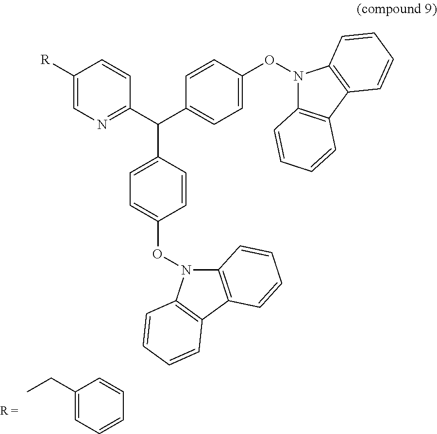
- the NMR spectrum of the compound 9 is shown in FIG. 4 .
- the ITO plate is washed in the ultrasonic cleaner using in an order of MeOH, acetone and isopropylalcohol (IPA) for 15 minutes to each cleaning solution and further washed using ionic-water. Then, the ITO plate is dried by annealing under 230° C. for 30 minutes.
- the compound 1 is dissolved in tetrachloroethane solvent, and the solution is coated on the ITO plate.
- An aluminum (Al) electrode is formed on the layer of the compound 7 by a thermal deposition process in a vacuum deposition apparatus such that an emitting diode (ITO/compound 7/Al) is fabricated. By applying voltages to the ITO plate and the Al electrode, the properties of the emitting diode using the compound 7 are tested.
- Example 1 The tested properties of Examples 1 to 3 and Comparative Example 1 are listed in Table 1, and I-V-L graphs in the emitting diode of Examples 1 to 3 and Comparative Example 1 are shown in FIG. 5 .
- the emitting diode using the emitting compound of the present invention has advantages in the emitting efficiency and the driving voltage in comparison to the emitting diode using CBP.
- the OLED device (or the emitting diode) using the emitting compound of the present invention can provide high quality images without thermal degradation and with improved lifetime.
- the emitting compound of the present invention has a main peak in a blue wave region and has advantages in brightness in comparison to the related art compound CBP.
Landscapes
- Chemical & Material Sciences (AREA)
- Engineering & Computer Science (AREA)
- Materials Engineering (AREA)
- Physics & Mathematics (AREA)
- Spectroscopy & Molecular Physics (AREA)
- Organic Chemistry (AREA)
- Electroluminescent Light Sources (AREA)
- Pyridine Compounds (AREA)
Abstract

wherein “A” is represented by

and “B” is represented by
Description

wherein each of R1 and R2 is independently selected from C1-C60 alkyl group, C2-C60 alkenyl group, C2-C60 alkynyl group, C5-C60 aryl group, C5-C60 heteroaryl group, C5-C40 aryloxy group, C1-C40 alkyloxy group, C1-C40 alkoxycarbonyl group, substituted or non-substituted amino group, halogen, cyano group, nitro group, hydroxyl group and carboxy group, and each of “m” and “n” is an integer of 0 (zero) to 4, wherein “A” is represented by

and each of R3 and R4 is independently selected from C1-C20 alkyl group, C2-C20 alkenyl group, C2-C20 alkynyl group, C1-C20 alkoxy group and a benzyl group, wherein each of “x” and “y” is an integer of 0 (zero) to 4, wherein “B” is represented by
and R5 is selected from halogen, C1-C60 alkyl group, C2-C60 alkenyl group, C2-C60 alkynyl group, a benzyl group and substituted or non-substituted anthracene, and wherein “z” is an integer of 0 (zero) to 4.


Each of R3 and R4 is independently selected from C1-C20 alkyl group, C2-C20 alkenyl group, C2-C20 alkynyl group, C1-C20 alkoxy group and a benzyl group. In this instance, the benzyl group may be substituted by C1-C20 alkyl. In addition, “x” and “y” respectively mean a number of the substituent, i.e., R3 and R4, for the phenyl ring of carbazole, and each of “x” and “y” is an integer of 0 (zero) to 4.
R5 is selected from halogen, C1-C60 alkyl group, C2-C60 alkenyl group, C2-C60 alkynyl group, a benzyl group and substituted or non-substituted anthracene. In this instance, the benzyl group may be substituted by C1-C60 alkyl. In addition, “z” means a number of the substituent, i.e., R5, for the pyridine ring, and “z” is an integer of 0 (zero) to 4.


(Compound 7)


(Compound 8)
| TABLE 1 | ||||
| Emitting | ||||
| Current density | Driving | efficiency | ||
| [mA/cm2] | voltage [V] | [cd/A] | ||
| Ex. 1 | |
10 | 5.2 | 5.4 |
| Ex. 2 | |
10 | 5.1 | 5.1 |
| Ex. 3 | Compound 9 | 10 | 4.8 | 5.7 |
| Com. 1 | |
10 | 6.3 | 4.5 |
| TABLE 2 | ||||
| current | ||||
| Current density | Driving | efficiency | ||
| [mA/cm2] | voltage [V] | [cd/A] | ||
| Ex. 4 | Compound 7: FIrpic | 10 | 4.8 | 5.7 |
| Ex. 5 | Compound 8: FIrpic | 10 | 4.6 | 5.5 |
| Ex. 6 | Compound 9: FIrpic | 10 | 4.4 | 5.8 |
| Com. 2 | CBP: |
10 | 5.3 | 5.2 |
Claims (7)


Applications Claiming Priority (2)
| Application Number | Priority Date | Filing Date | Title |
|---|---|---|---|
| KR1020120132888A KR101957149B1 (en) | 2012-11-22 | 2012-11-22 | Blue Luminescent Compounds and Organic Electroluminescence Device Using the Same |
| KR10-2012-00132888 | 2012-11-22 |
Publications (2)
| Publication Number | Publication Date |
|---|---|
| US20140138657A1 US20140138657A1 (en) | 2014-05-22 |
| US9496507B2 true US9496507B2 (en) | 2016-11-15 |
Family
ID=50727106
Family Applications (1)
| Application Number | Title | Priority Date | Filing Date |
|---|---|---|---|
| US14/084,425 Active 2035-02-18 US9496507B2 (en) | 2012-11-22 | 2013-11-19 | Emitting compound and organic light emitting diode device using the same |
Country Status (3)
| Country | Link |
|---|---|
| US (1) | US9496507B2 (en) |
| KR (1) | KR101957149B1 (en) |
| CN (1) | CN103833732B (en) |
Families Citing this family (1)
| Publication number | Priority date | Publication date | Assignee | Title |
|---|---|---|---|---|
| CN105646343A (en) * | 2016-01-30 | 2016-06-08 | 湖南大学 | Method for synthesizing aza-aryl-phenolic-ketone compound |
Citations (6)
| Publication number | Priority date | Publication date | Assignee | Title |
|---|---|---|---|---|
| KR20110112098A (en) | 2010-04-06 | 2011-10-12 | 다우어드밴스드디스플레이머티리얼 유한회사 | Novel organic light emitting compound and organic electroluminescent device employing the same |
| KR20110134201A (en) | 2010-06-08 | 2011-12-14 | 덕산하이메탈(주) | Compound containing carbazole and aromatic amine derivative and organic electric device using same, terminal thereof |
| US20120256173A1 (en) * | 2010-01-15 | 2012-10-11 | Fujifilm Corporation | Charge transporting material and organic electroluminescence device |
| US20120280218A1 (en) * | 2010-01-15 | 2012-11-08 | Fujifilm Corporation | Organic electroluminescence device |
| US20120292607A1 (en) * | 2010-01-15 | 2012-11-22 | Fujifilm Corporation | Organic electroluminescence device |
| US20120298977A1 (en) * | 2010-01-15 | 2012-11-29 | Fujifilm Corporation | Organic electroluminescence device |
Family Cites Families (4)
| Publication number | Priority date | Publication date | Assignee | Title |
|---|---|---|---|---|
| US7597967B2 (en) * | 2004-12-17 | 2009-10-06 | Eastman Kodak Company | Phosphorescent OLEDs with exciton blocking layer |
| WO2010061315A1 (en) * | 2008-11-26 | 2010-06-03 | Philips Intellectual Property & Standards Gmbh | Oled with novel hole-conducting material |
| WO2012016074A1 (en) * | 2010-07-29 | 2012-02-02 | University Of Southern California | Co-deposition methods for the fabrication of organic optoelectronic devices |
| FR2975911A1 (en) | 2011-06-06 | 2012-12-07 | Univ Strasbourg | BISACODYL AND THE LIKE AS MEDICAMENTS FOR THE TREATMENT OF CANCER |
-
2012
- 2012-11-22 KR KR1020120132888A patent/KR101957149B1/en active Active
-
2013
- 2013-11-19 US US14/084,425 patent/US9496507B2/en active Active
- 2013-11-22 CN CN201310597284.2A patent/CN103833732B/en active Active
Patent Citations (6)
| Publication number | Priority date | Publication date | Assignee | Title |
|---|---|---|---|---|
| US20120256173A1 (en) * | 2010-01-15 | 2012-10-11 | Fujifilm Corporation | Charge transporting material and organic electroluminescence device |
| US20120280218A1 (en) * | 2010-01-15 | 2012-11-08 | Fujifilm Corporation | Organic electroluminescence device |
| US20120292607A1 (en) * | 2010-01-15 | 2012-11-22 | Fujifilm Corporation | Organic electroluminescence device |
| US20120298977A1 (en) * | 2010-01-15 | 2012-11-29 | Fujifilm Corporation | Organic electroluminescence device |
| KR20110112098A (en) | 2010-04-06 | 2011-10-12 | 다우어드밴스드디스플레이머티리얼 유한회사 | Novel organic light emitting compound and organic electroluminescent device employing the same |
| KR20110134201A (en) | 2010-06-08 | 2011-12-14 | 덕산하이메탈(주) | Compound containing carbazole and aromatic amine derivative and organic electric device using same, terminal thereof |
Also Published As
| Publication number | Publication date |
|---|---|
| CN103833732B (en) | 2016-01-20 |
| US20140138657A1 (en) | 2014-05-22 |
| KR20140065882A (en) | 2014-05-30 |
| CN103833732A (en) | 2014-06-04 |
| KR101957149B1 (en) | 2019-03-12 |
Similar Documents
| Publication | Publication Date | Title |
|---|---|---|
| KR101773936B1 (en) | New organic electroluminescent compounds and organic electroluminescent device comprising the same | |
| KR101738607B1 (en) | Organic electroluminescent device | |
| US6723445B2 (en) | Organic light-emitting devices | |
| US8962158B2 (en) | Material having indolocarbazole compound for phosphorescent light-emitting element and organic electroluminescent element using the same | |
| KR101847578B1 (en) | Fused aromatic compounds and organic light-emitting diode including the same | |
| US10411199B2 (en) | Organometallic complexes, and organic electroluminescent device and display using the same | |
| US9343685B2 (en) | Organic electroluminescent element | |
| JP2023532856A (en) | Organic electronic devices and display devices comprising organic electronic devices, and compositions for use in organic electronic devices | |
| US9543527B2 (en) | Red phosphorescent compound and organic light emitting diode device using the same | |
| US9123898B2 (en) | Phosphorescent compound and organic light emitting diode device using the same | |
| US20160164003A1 (en) | Organic light emitting display device | |
| KR102152013B1 (en) | Organic light emitting diode device comprising organic compounds | |
| JP2020037523A (en) | Benzothienobenzothiophene derivative, hole transport material comprising the same, and organic EL device using the same | |
| KR102493459B1 (en) | N-heterocyclic compound and organic light emitting device comprising the same | |
| US9496507B2 (en) | Emitting compound and organic light emitting diode device using the same | |
| US8987472B2 (en) | N-cycloalkylalkyl triscarbazoles | |
| KR20150095208A (en) | Novel hole injecting· hole-transporting compound and organic electroluminescent device comprising same | |
| KR20150065146A (en) | Novel compound and organic electroluminescent device comprising same | |
| KR20230028185A (en) | Compound and organic light emitting device comprising the same | |
| KR20230018162A (en) | Compound and organic light emitting device comprising same | |
| JP2020510318A (en) | Organic light emitting device and method of manufacturing the same | |
| KR20240150720A (en) | Compound and organic light emitting device comprising the same | |
| KR20240150721A (en) | Compound and organic light emitting device comprising the same | |
| US20140175401A1 (en) | Red phosphorescent compound and organic light emitting diode device using the same | |
| KR20240150722A (en) | Compound and organic light emitting device comprising the same |
Legal Events
| Date | Code | Title | Description |
|---|---|---|---|
| AS | Assignment |
Owner name: LG DISPLAY CO., LTD., KOREA, REPUBLIC OF Free format text: ASSIGNMENT OF ASSIGNORS INTEREST;ASSIGNOR:KIM, YOUNG-JU;REEL/FRAME:031654/0182 Effective date: 20131115 |
|
| STCF | Information on status: patent grant |
Free format text: PATENTED CASE |
|
| FEPP | Fee payment procedure |
Free format text: PAYOR NUMBER ASSIGNED (ORIGINAL EVENT CODE: ASPN); ENTITY STATUS OF PATENT OWNER: LARGE ENTITY |
|
| MAFP | Maintenance fee payment |
Free format text: PAYMENT OF MAINTENANCE FEE, 4TH YEAR, LARGE ENTITY (ORIGINAL EVENT CODE: M1551); ENTITY STATUS OF PATENT OWNER: LARGE ENTITY Year of fee payment: 4 |
|
| MAFP | Maintenance fee payment |
Free format text: PAYMENT OF MAINTENANCE FEE, 8TH YEAR, LARGE ENTITY (ORIGINAL EVENT CODE: M1552); ENTITY STATUS OF PATENT OWNER: LARGE ENTITY Year of fee payment: 8 |