US9494827B2 - Liquid crystal device, electronic apparatus, and method for manufacturing liquid crystal device - Google Patents
Liquid crystal device, electronic apparatus, and method for manufacturing liquid crystal device Download PDFInfo
- Publication number
- US9494827B2 US9494827B2 US14/541,457 US201414541457A US9494827B2 US 9494827 B2 US9494827 B2 US 9494827B2 US 201414541457 A US201414541457 A US 201414541457A US 9494827 B2 US9494827 B2 US 9494827B2
- Authority
- US
- United States
- Prior art keywords
- liquid crystal
- substrate
- alignment film
- alignment
- electrode
- Prior art date
- Legal status (The legal status is an assumption and is not a legal conclusion. Google has not performed a legal analysis and makes no representation as to the accuracy of the status listed.)
- Active, expires
Links
Images


Classifications
-
- G—PHYSICS
- G02—OPTICS
- G02B—OPTICAL ELEMENTS, SYSTEMS OR APPARATUS
- G02B30/00—Optical systems or apparatus for producing three-dimensional [3D] effects, e.g. stereoscopic images
- G02B30/20—Optical systems or apparatus for producing three-dimensional [3D] effects, e.g. stereoscopic images by providing first and second parallax images to an observer's left and right eyes
- G02B30/26—Optical systems or apparatus for producing three-dimensional [3D] effects, e.g. stereoscopic images by providing first and second parallax images to an observer's left and right eyes of the autostereoscopic type
- G02B30/27—Optical systems or apparatus for producing three-dimensional [3D] effects, e.g. stereoscopic images by providing first and second parallax images to an observer's left and right eyes of the autostereoscopic type involving lenticular arrays
- G02B30/28—Optical systems or apparatus for producing three-dimensional [3D] effects, e.g. stereoscopic images by providing first and second parallax images to an observer's left and right eyes of the autostereoscopic type involving lenticular arrays involving active lenticular arrays
-
- G—PHYSICS
- G02—OPTICS
- G02F—OPTICAL DEVICES OR ARRANGEMENTS FOR THE CONTROL OF LIGHT BY MODIFICATION OF THE OPTICAL PROPERTIES OF THE MEDIA OF THE ELEMENTS INVOLVED THEREIN; NON-LINEAR OPTICS; FREQUENCY-CHANGING OF LIGHT; OPTICAL LOGIC ELEMENTS; OPTICAL ANALOGUE/DIGITAL CONVERTERS
- G02F1/00—Devices or arrangements for the control of the intensity, colour, phase, polarisation or direction of light arriving from an independent light source, e.g. switching, gating or modulating; Non-linear optics
- G02F1/01—Devices or arrangements for the control of the intensity, colour, phase, polarisation or direction of light arriving from an independent light source, e.g. switching, gating or modulating; Non-linear optics for the control of the intensity, phase, polarisation or colour
- G02F1/13—Devices or arrangements for the control of the intensity, colour, phase, polarisation or direction of light arriving from an independent light source, e.g. switching, gating or modulating; Non-linear optics for the control of the intensity, phase, polarisation or colour based on liquid crystals, e.g. single liquid crystal display cells
- G02F1/133—Constructional arrangements; Operation of liquid crystal cells; Circuit arrangements
- G02F1/1333—Constructional arrangements; Manufacturing methods
- G02F1/1337—Surface-induced orientation of the liquid crystal molecules, e.g. by alignment layers
- G02F1/13378—Surface-induced orientation of the liquid crystal molecules, e.g. by alignment layers by treatment of the surface, e.g. embossing, rubbing or light irradiation
-
- G02B27/2214—
-
- G—PHYSICS
- G02—OPTICS
- G02B—OPTICAL ELEMENTS, SYSTEMS OR APPARATUS
- G02B30/00—Optical systems or apparatus for producing three-dimensional [3D] effects, e.g. stereoscopic images
- G02B30/20—Optical systems or apparatus for producing three-dimensional [3D] effects, e.g. stereoscopic images by providing first and second parallax images to an observer's left and right eyes
- G02B30/26—Optical systems or apparatus for producing three-dimensional [3D] effects, e.g. stereoscopic images by providing first and second parallax images to an observer's left and right eyes of the autostereoscopic type
- G02B30/27—Optical systems or apparatus for producing three-dimensional [3D] effects, e.g. stereoscopic images by providing first and second parallax images to an observer's left and right eyes of the autostereoscopic type involving lenticular arrays
-
- G—PHYSICS
- G02—OPTICS
- G02F—OPTICAL DEVICES OR ARRANGEMENTS FOR THE CONTROL OF LIGHT BY MODIFICATION OF THE OPTICAL PROPERTIES OF THE MEDIA OF THE ELEMENTS INVOLVED THEREIN; NON-LINEAR OPTICS; FREQUENCY-CHANGING OF LIGHT; OPTICAL LOGIC ELEMENTS; OPTICAL ANALOGUE/DIGITAL CONVERTERS
- G02F1/00—Devices or arrangements for the control of the intensity, colour, phase, polarisation or direction of light arriving from an independent light source, e.g. switching, gating or modulating; Non-linear optics
- G02F1/01—Devices or arrangements for the control of the intensity, colour, phase, polarisation or direction of light arriving from an independent light source, e.g. switching, gating or modulating; Non-linear optics for the control of the intensity, phase, polarisation or colour
- G02F1/13—Devices or arrangements for the control of the intensity, colour, phase, polarisation or direction of light arriving from an independent light source, e.g. switching, gating or modulating; Non-linear optics for the control of the intensity, phase, polarisation or colour based on liquid crystals, e.g. single liquid crystal display cells
- G02F1/133—Constructional arrangements; Operation of liquid crystal cells; Circuit arrangements
- G02F1/1333—Constructional arrangements; Manufacturing methods
- G02F1/1337—Surface-induced orientation of the liquid crystal molecules, e.g. by alignment layers
- G02F1/13378—Surface-induced orientation of the liquid crystal molecules, e.g. by alignment layers by treatment of the surface, e.g. embossing, rubbing or light irradiation
- G02F1/133784—Surface-induced orientation of the liquid crystal molecules, e.g. by alignment layers by treatment of the surface, e.g. embossing, rubbing or light irradiation by rubbing
-
- G—PHYSICS
- G02—OPTICS
- G02F—OPTICAL DEVICES OR ARRANGEMENTS FOR THE CONTROL OF LIGHT BY MODIFICATION OF THE OPTICAL PROPERTIES OF THE MEDIA OF THE ELEMENTS INVOLVED THEREIN; NON-LINEAR OPTICS; FREQUENCY-CHANGING OF LIGHT; OPTICAL LOGIC ELEMENTS; OPTICAL ANALOGUE/DIGITAL CONVERTERS
- G02F1/00—Devices or arrangements for the control of the intensity, colour, phase, polarisation or direction of light arriving from an independent light source, e.g. switching, gating or modulating; Non-linear optics
- G02F1/01—Devices or arrangements for the control of the intensity, colour, phase, polarisation or direction of light arriving from an independent light source, e.g. switching, gating or modulating; Non-linear optics for the control of the intensity, phase, polarisation or colour
- G02F1/13—Devices or arrangements for the control of the intensity, colour, phase, polarisation or direction of light arriving from an independent light source, e.g. switching, gating or modulating; Non-linear optics for the control of the intensity, phase, polarisation or colour based on liquid crystals, e.g. single liquid crystal display cells
- G02F1/133—Constructional arrangements; Operation of liquid crystal cells; Circuit arrangements
- G02F1/1333—Constructional arrangements; Manufacturing methods
- G02F1/1337—Surface-induced orientation of the liquid crystal molecules, e.g. by alignment layers
- G02F1/13378—Surface-induced orientation of the liquid crystal molecules, e.g. by alignment layers by treatment of the surface, e.g. embossing, rubbing or light irradiation
- G02F1/133788—Surface-induced orientation of the liquid crystal molecules, e.g. by alignment layers by treatment of the surface, e.g. embossing, rubbing or light irradiation by light irradiation, e.g. linearly polarised light photo-polymerisation
-
- G—PHYSICS
- G02—OPTICS
- G02F—OPTICAL DEVICES OR ARRANGEMENTS FOR THE CONTROL OF LIGHT BY MODIFICATION OF THE OPTICAL PROPERTIES OF THE MEDIA OF THE ELEMENTS INVOLVED THEREIN; NON-LINEAR OPTICS; FREQUENCY-CHANGING OF LIGHT; OPTICAL LOGIC ELEMENTS; OPTICAL ANALOGUE/DIGITAL CONVERTERS
- G02F1/00—Devices or arrangements for the control of the intensity, colour, phase, polarisation or direction of light arriving from an independent light source, e.g. switching, gating or modulating; Non-linear optics
- G02F1/29—Devices or arrangements for the control of the intensity, colour, phase, polarisation or direction of light arriving from an independent light source, e.g. switching, gating or modulating; Non-linear optics for the control of the position or the direction of light beams, i.e. deflection
-
- G—PHYSICS
- G02—OPTICS
- G02F—OPTICAL DEVICES OR ARRANGEMENTS FOR THE CONTROL OF LIGHT BY MODIFICATION OF THE OPTICAL PROPERTIES OF THE MEDIA OF THE ELEMENTS INVOLVED THEREIN; NON-LINEAR OPTICS; FREQUENCY-CHANGING OF LIGHT; OPTICAL LOGIC ELEMENTS; OPTICAL ANALOGUE/DIGITAL CONVERTERS
- G02F1/00—Devices or arrangements for the control of the intensity, colour, phase, polarisation or direction of light arriving from an independent light source, e.g. switching, gating or modulating; Non-linear optics
- G02F1/01—Devices or arrangements for the control of the intensity, colour, phase, polarisation or direction of light arriving from an independent light source, e.g. switching, gating or modulating; Non-linear optics for the control of the intensity, phase, polarisation or colour
- G02F1/13—Devices or arrangements for the control of the intensity, colour, phase, polarisation or direction of light arriving from an independent light source, e.g. switching, gating or modulating; Non-linear optics for the control of the intensity, phase, polarisation or colour based on liquid crystals, e.g. single liquid crystal display cells
- G02F1/133—Constructional arrangements; Operation of liquid crystal cells; Circuit arrangements
- G02F1/1333—Constructional arrangements; Manufacturing methods
- G02F1/1339—Gaskets; Spacers; Sealing of cells
- G02F1/13394—Gaskets; Spacers; Sealing of cells spacers regularly patterned on the cell subtrate, e.g. walls, pillars
-
- G—PHYSICS
- G02—OPTICS
- G02F—OPTICAL DEVICES OR ARRANGEMENTS FOR THE CONTROL OF LIGHT BY MODIFICATION OF THE OPTICAL PROPERTIES OF THE MEDIA OF THE ELEMENTS INVOLVED THEREIN; NON-LINEAR OPTICS; FREQUENCY-CHANGING OF LIGHT; OPTICAL LOGIC ELEMENTS; OPTICAL ANALOGUE/DIGITAL CONVERTERS
- G02F1/00—Devices or arrangements for the control of the intensity, colour, phase, polarisation or direction of light arriving from an independent light source, e.g. switching, gating or modulating; Non-linear optics
- G02F1/29—Devices or arrangements for the control of the intensity, colour, phase, polarisation or direction of light arriving from an independent light source, e.g. switching, gating or modulating; Non-linear optics for the control of the position or the direction of light beams, i.e. deflection
- G02F1/294—Variable focal length devices
-
- G02F2001/294—
-
- H04N13/0404—
-
- H—ELECTRICITY
- H04—ELECTRIC COMMUNICATION TECHNIQUE
- H04N—PICTORIAL COMMUNICATION, e.g. TELEVISION
- H04N13/00—Stereoscopic video systems; Multi-view video systems; Details thereof
- H04N13/30—Image reproducers
- H04N13/302—Image reproducers for viewing without the aid of special glasses, i.e. using autostereoscopic displays
- H04N13/305—Image reproducers for viewing without the aid of special glasses, i.e. using autostereoscopic displays using lenticular lenses, e.g. arrangements of cylindrical lenses
Definitions
- the present disclosure relates to a liquid crystal device, an electronic apparatus provided with the liquid crystal device, and a method for manufacturing the liquid crystal device.
- liquid crystal display In a liquid crystal display (LCD), there has been a device capable of displaying a stereoscopic image viewable with the naked eyes of a user.
- This type of liquid crystal display includes a mechanism that arranges a liquid crystal device such as a variable lens array on the surface of the liquid crystal display that displays an image thereon as a mechanism that generates parallax in user's eyes.
- the liquid crystal display having a variable lens array utilizes the refractive index of the liquid crystal of the variable lens array to divide an image displayed on an image display device into two in conformity with a right-and-left parallax and generate a parallax of the images that reach respective right-and-left eyes of a user thus constituting an image that is stereophonically viewable.
- the liquid crystal device constitutes the variable lens array
- a pair of substrates needs to be separated with a predetermined distance therebetween.
- the liquid crystal layer of the variable lens array becomes considerably thicker compared with a liquid crystal layer of a general liquid crystal display panel.
- the liquid crystal device has a structure such that spacers are provided between two substrates that sandwich a liquid crystal layer to maintain the thickness of the liquid crystal layer.
- the spacers are positioned at random, a liquid crystal lens varies in shape depending on the position thereof and hence, there may be a case that the characteristics of the lens are unstable.
- the pillar spacers can be formed in a desired pattern by the process that uses lithography and etching.
- the liquid crystal device of the variable lens array uses, for example, a vertical alignment (VA) mode liquid crystal.
- VA vertical alignment
- Liquid crystal molecules of the liquid crystal device are aligned in such a manner that the major axis direction thereof is aligned along a direction perpendicular to the surface of the substrate when applying no voltage (in an OFF state), and aligned in such a manner that the liquid crystal molecules tilt (incline) depending on the level of the voltage when applying a voltage (in an ON state).
- the liquid crystal molecules tilt in arbitrary directions, giving rise to the possibility of the alignment disorder of the liquid crystal molecules and the occurrence of an abnormal alignment (a reverse twisted domain, for example).
- an abnormal alignment a reverse twisted domain, for example.
- the abnormal alignment easily occurs. In the place in which the abnormal alignment occurs, the failure with a display defect occurs and thus causes deterioration in yield.
- a liquid crystal device includes: a first substrate, the first substrate being transparent; a second substrate disposed opposite the first substrate, the second substrate being transparent; a liquid crystal layer provided between the first substrate and the second substrate, the liquid crystal layer including liquid crystal molecules; an alignment film with alignment treatment such that the liquid crystal molecules align, the alignment film being provided on a surface of the first substrate, the surface facing the liquid crystal layer; and pillar spacers provided on the alignment film, wherein the alignment treatment is applied to the alignment film except at least a part of area in which each of the pillar spacers overlaps with the alignment film.
- the electronic apparatus of the present disclosure is provided with the above-mentioned liquid crystal device, and corresponds, for example, to a handheld terminal device or a handheld information terminal, such as a car navigation device, a television apparatus, a digital camera, a personal computer, a video camera, a mobile phone, and a portable game machine.
- a handheld terminal device or a handheld information terminal such as a car navigation device, a television apparatus, a digital camera, a personal computer, a video camera, a mobile phone, and a portable game machine.
- a method for manufacturing a liquid crystal device includes a first substrate, the first substrate being transparent; a second substrate disposed opposite the first substrate, the second substrate being transparent; a liquid crystal layer provided between the first substrate and the second substrate, the liquid crystal layer including liquid crystal molecules; an alignment film with alignment treatment such that the liquid crystal molecules align, the alignment film being provided on a surface of the first substrate, the surface facing the liquid crystal layer; and pillar spacers provided on the alignment film, wherein the alignment treatment is applied to the alignment film except at least a part of area in which each of the pillar spacers overlaps with the alignment film.
- the method includes: forming a film to be an alignment film on the first substrate; forming pillar spacers on the film; and applying alignment treatment to the film the pillar spacers having been formed thereon, so that the film comes into the alignment film.
- the liquid crystal device According to the liquid crystal device, the electronic apparatus, and the method for manufacturing the liquid crystal device in the present disclosure, failures due to an abnormal alignment and the deterioration in yield can be suppressed.
- FIG. 1 is an exploded schematic perspective view of an image display device according to the embodiment
- FIG. 2 is a sectional view illustrating the schematic section structure of an image display unit
- FIG. 3 is a sectional view illustrating the schematic section structure of a variable lens array.
- FIG. 4 is a schematic view illustrating the pre-tilt angle of liquid crystal molecules
- FIG. 5 is a schematic plan view of the variable lens array as viewed in a front view
- FIG. 6 is a schematic plan view of the variable lens array as viewed in a rear view
- FIG. 7 is a flowchart for explaining one example of a method for manufacturing a liquid crystal device
- FIG. 8 is an explanatory view for explaining one example of the method for manufacturing the liquid crystal device
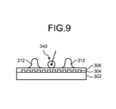
- FIG. 9 is an explanatory view for explaining another example of the method for manufacturing the liquid crystal device.
- FIG. 10 is an exploded schematic perspective view of an image display device according to another embodiment.
- FIG. 11 is a view illustrating one example of an electronic apparatus that applies the image display device according to the present embodiment thereto.
- FIG. 1 is an exploded schematic perspective view of an image display device according to the present embodiment.
- an image display device 1 is provided with an image display unit 10 that displays a two-dimensional image, an illumination unit 20 , and a variable lens array (a liquid crystal device) 30 .
- the image display unit 10 displays a two-dimensional image thereon.
- the image display unit 10 includes a display area 11 having M pieces of pixels 12 arranged in the X direction illustrated in FIG. 1 and N pieces of pixels 12 arranged in the Y direction illustrated in FIG. 1 .
- the image display unit 10 in the present embodiment is a liquid crystal display panel.
- a well-known image display device such as an electroluminescence display panel or a plasma display panel can be used as the image display unit 10 .
- the image display unit 10 may display a monochrome image and may also display a color image.
- the liquid crystal display panel comprises, for example, a front panel provided with transparent common electrodes, a rear panel provided with transparent pixel electrodes, and a liquid crystal material arranged between the front panel and the rear panel.
- the operational mode of the liquid crystal display panel is not particularly limited.
- the liquid crystal display panel may be driven in a so-called TN mode, and may be driven in a VA mode or in an IPS mode.
- FIG. 2 is a sectional view illustrating the schematic section structure of the image display unit.
- the display area 11 of the image display unit 10 is provided with a pixel substrate 11 A, a counter substrate 11 B arranged in an opposed manner in the direction perpendicular to the surface of the pixel substrate 11 A, and a liquid crystal layer 11 C inserted into a space between the pixel substrate 11 A and the counter substrate 11 B.
- a distance between the pixel substrate 11 A and the counter substrate 11 B is approximately 3 ⁇ m to 4 ⁇ m, for example.
- the liquid crystal layer 11 C modulates a light passing therethrough depending on a state of an electric field and, for example, liquid crystals in various kinds of modes such as Twisted Nematic (TN), Vertical Alignment (VA), Electrically Controlled Birefringence (ECB), and Fringe Field Switching (FFS) are used for the liquid crystal layer 11 C.
- TN Twisted Nematic
- VA Vertical Alignment
- EBC Electrically Controlled Birefringence
- FFS Fringe Field Switching
- the counter substrate 11 B includes a glass substrate 75 and a color filter 76 formed on one surface of the glass substrate 75 .
- a polarizer 73 A is arranged on the other surface of the glass substrate 75 .
- the color filter 76 includes color regions colored in the three colors of red (R), green (G), and blue (B).
- the color filter 76 cyclically arranges therein the respective color regions that are colored in the three colors of red (R), green (G), and blue (B). Color regions colored in the three colors of R, G, and B correspond to each pixel as one set of pixel.
- the color filter 76 faces the liquid crystal layer 11 C in an opposed manner in a direction perpendicular to a TFT substrate 71 .
- the color filter 76 may use any other colors in combination provided that the colors are different from each other. Generally, in the color filter 76 , the luminance of the color region of green (G) is higher than that of each of the color region of red (R) and the color region of blue (B).
- a common electrode COML is a transparent electrode formed of a transparent conductive material (transparent conducting oxide), such as Indium Tin Oxide (ITO).
- the pixel substrate 11 A includes the TFT substrate 71 as a circuit board, a plurality of pixel electrodes 72 arranged in a matrix array on the TFT substrate 71 , a common electrode COML formed in between the TFT substrate 71 and the pixel electrode 72 , an insulating layer 74 that insulates the pixel electrode 72 from the common electrode COML, and an incident-side polarizer 73 B arranged on the bottom side of the TFT substrate 71 .
- a first alignment film 77 is arranged in between the liquid crystal layer 11 C and the pixel substrate 11 A.
- a second alignment film 78 is arranged in between the liquid crystal layer 11 C and the counter substrate 11 B.
- the image display unit 10 is driven by a drive circuit that is not illustrated in the drawings, and controls the alignment direction of liquid crystal molecules in a pixel thus displaying a two-dimensional image corresponding to a video signal from the outside.
- the illumination unit 20 that radiates light is arranged on the back side of the image display unit 10 .
- the illumination unit 20 is provided with members such as a light source, a prism sheet, a diffusion sheet, and a light guide plate (these members are not illustrated in the drawings).
- a well-known illumination unit can be used as the illumination unit 20 .
- the illumination unit 20 is not limited in particular.
- FIG. 3 is a sectional view illustrating the schematic section structure of the variable lens array.
- FIG. 4 is a schematic view illustrating the pretilt angle of liquid crystal molecules.
- FIG. 5 is a schematic plan view of the variable lens array as viewed in a front view.
- FIG. 6 is a schematic plan view of the variable lens array as viewed in a rear view.
- FIG. 5 is a view with a part cut out of a second substrate 130 B.
- FIG. 6 is a view with a part cut out of a first substrate 130 A.
- variable lens array 30 is provided with the first substrate 130 A, the second substrate 130 B, and a liquid crystal layer 137 arranged in between the first substrate 130 A and the second substrate 130 B.
- a sealing member 138 is formed in the circumferences of the surfaces of the first substrate 130 A and the second substrate 130 B that face each other in an opposed manner, and has a mechanism of sealing between the first substrate 130 A and the second substrate 130 B.
- a material with high light transmissivity can be used for the first substrate 130 A and the second substrate 130 B.
- a material that forms each of the first substrate 130 A and the second substrate 130 B for example, acrylic resin, polycarbonate resin (PC), ABS resin, polymethyl methacrylate resin (PMMA), polyarylate resin (PAR), polyethylene terephthalate resin (PET), or glass can be exemplified.
- the materials of the first substrate 130 A and the second substrate 130 B may be identical with each other, and may be different from each other.
- the variable lens array 30 is arranged to face the front face of the image display unit 10 in an opposed manner, and held by a holding member that is not illustrated in the drawings so that the variable lens array 30 and the image display unit 10 are separated with a predetermined distance therebetween in terms of specification.
- the front face of the image display unit 10 means the face closer to an image viewer who views an image displayed on the image display unit 10 .
- spacers (pillar spacers) 136 are arranged in between the first substrate 130 A and the second substrate 130 B of the variable lens array 30 , at the place such that the alignment direction of the liquid crystal molecules in the liquid crystal layer 137 does not change when the refractive index of each of columns of lens 31 is changed.
- variable lens array 30 P pieces of the columns of lens (variable column of lens) 31 extending in the Y direction illustrated in FIG. 1 are arranged next to each other in the X direction illustrated in FIG. 1 .
- the column of lens 31 p is adjacent to a column of lens 31 p ⁇ 1 and a column of lens 31 p+1 .
- the relationship between “P” and “M” mentioned above is described later.
- the number of viewpoints on the image when displaying a stereoscopic image is four (4); that is, viewpoints A1, A2, . . . , and A4, in a central viewing area.
- this assumption merely constitutes one exemplification.
- the number of viewing areas and the number of viewpoints can be appropriately set depending on the specification of the image display device 1 .
- the image for each viewpoint becomes viewable also in the areas on the left side and the right side of the central viewing area.
- variable lens array 30 that is a liquid crystal device is provided with the column of lens 31 each of which changes the alignment direction of the liquid crystal molecules in the liquid crystal layer 137 by a voltage applied between a first electrode 131 and a second electrode 134 thus changing the refractive index thereof.
- the variable lens array 30 includes the first substrate 130 A having first electrodes 131 1 , 131 2 , . . . , and 131 8 , the second substrate 130 B having the second electrode 134 , and the liquid crystal layer 137 arranged in between the first substrate 130 A and the second substrate 130 B.
- the first electrodes 131 1 , 131 2 , . . . , and 131 8 may be referred to collectively as the first electrode 131 .
- Other constitutional features may also be referred to in the same manner as above.
- the first electrode 131 and the second electrode 134 are formed on the respective surfaces (inner surfaces) on the liquid-crystal-layer- 137 -sides of the first substrate 130 A and the second substrate 130 B.
- the liquid crystal layer 137 is composed of a positive nematic liquid crystal material.
- the liquid crystal layer 137 in the present embodiment uses a homogeneously aligned liquid crystal material.
- Each of the first electrode 131 and the second electrode 134 is formed of a transparent conductive material such as ITO, and formed by film formation.
- the first electrode 131 is formed in a predetermined striped shape illustrated in FIG. 5 by patterning.
- the second electrode 134 is a so-called common electrode, and is formed on the whole surface of the second substrate 130 B.
- FIG. 6 the illustrations of the second electrode 134 and a second alignment film 135 described later are omitted.
- FIG. 5 also, the illustration of a first alignment film 133 described later is omitted.
- the first alignment film 133 that covers the whole surface of the first substrate 130 A including the first electrode 131 is formed on the first substrate 130 A
- the second alignment film 135 that covers the whole surface of the second substrate 130 B including the second electrode 134 is formed on the second substrate 130 B.
- Each of the alignment films is, for example, formed of a polyimide material, and alignment treatment such as rubbing treatment is applied to the surface of each alignment film.
- the first alignment film 133 and the second alignment film 135 specify the direction of the molecular axis of liquid crystal molecules 137 A in a state that an electric field is not applied.
- the alignment treatment described below is applied; that is, the alignment treatment turns the longitudinal axis of the liquid crystal molecules 137 A to the Y direction in a state that an electric field is not applied to the liquid crystal molecules 137 A, and turns the longitudinal axis of the liquid crystal molecules 137 A to the Z direction in a state that an electric field is applied to the liquid crystal molecules 137 A.
- FIG. 3 illustrates the alignment of the liquid crystal molecules 137 A to which the electric field is not applied.
- a predetermined voltage is applied to the second electrode 134 from a drive circuit that is not illustrated in the drawings.
- grooves 133 A are formed by alignment treatment.
- Liquid crystal molecules 137 AA that are in the vicinity of the first alignment film 133 have a pretilt angle such that the groove 133 A tilts the corresponding liquid crystal molecule 137 AA by a predetermined angle with respect to the surface of the first substrate 130 A.
- grooves 135 A are formed by the alignment treatment.
- Liquid crystal molecules 137 AB that are in the vicinity of the second alignment film 135 have a pretilt angle such that the corresponding groove 135 A tilts the liquid crystal molecule 137 AB by a predetermined angle with respect to the surface of the second substrate 130 B.
- the groove 133 A formed in the first alignment film 133 and the groove 135 A formed in the second alignment film 135 may be formed in the identical shape so that the pretilt angles thereof are identical with each other.
- FIG. 4 illustrates an example that performs rubbing treatment as the alignment treatment. As the alignment treatment, photo alignment treatment may be performed.
- one column of lens 31 basically corresponds to pixels 12 in four rows.
- the respective pitches of the column of lens 31 and the pixels 12 in the X direction illustrated in FIG. 1 are expressed as a numeral LD and a numeral ND
- the relationship between the numeral LD and the numeral ND is such that LD ⁇ 4 ⁇ ND in the case of the 3D of four viewpoints
- the relationship between the numeral LD and the numeral ND is such that LD ⁇ 2 ⁇ ND in the case of the 3D of two viewpoints.
- the relationship between “P” and “M” that are mentioned above is such that P ⁇ M/4.
- the first electrodes 131 1 , 131 2 , . . . , and 131 8 each of which is formed in a stripe shape extending in the Y direction illustrated in FIG. 3 and FIG. 5 are arranged.
- the first electrodes 131 are arranged next to each other in the X direction separated with a predetermined distance NW therebetween.
- a numeral EW indicates the width of the first electrode 131 in the X direction.
- the number of the first electrodes 131 corresponding to one column of lens 31 is not limited to eight (8), and may be appropriately changed depending on the specification of the variable lens array 30 .
- the values of the distance NW and the width EW are not limited in particular, and may be, for example, appropriately set to preferred values in consideration of film formation and patterning techniques.
- the second electrode 134 is a planar electrode formed on the whole surface of the second substrate 130 B. However, when there is at least one electrode between two columns of lens 31 adjacent to each other, the column of lens 31 can be formed. Accordingly, it is necessary only to form at least one second electrode 134 between two columns of lens 31 adjacent to each other, and it is unnecessary to form the second electrode 134 on the whole surface of the second substrate 130 B.
- the second electrode 134 When the second electrode 134 is formed in a stripe shape, the second electrode 134 can be formed in the direction orthogonal to the direction in which the first electrode 131 extends. Due to the structure mentioned above, a variable lens suitable for 3D viewing is obtained.
- the second electrode 134 may be formed in parallel with the direction in which the first electrode 131 extends.
- electric supply lines 132 1 , 132 2 , . . . , and 132 4 each of which extends in a stripe shape in the X direction illustrated in FIG. 5 are further provided.
- the electric supply lines 132 1 to 132 4 are also formed basically by the same manufacturing process as the case of the first electrode 131 .
- the first electrodes 131 1 and 131 8 are connected to the electric supply line 132 1
- the first electrodes 131 2 and 131 7 are connected to the electric supply line 132 2 .
- the first electrodes 131 3 and 131 6 are connected to the electric supply line 132 3 , and the first electrodes 131 4 and 131 5 are connected to the electric supply line 132 4 .
- FIG. 5 the illustration of a contact between an electric supply line 132 and the electrode 131 is omitted.
- the voltage of each of the first electrodes 131 1 and 131 8 is controlled by a voltage applied to the electric supply line 132 1
- the voltage of each of the first electrodes 131 2 and 131 7 is controlled by a voltage applied to the electric supply line 132 2
- the voltage of each of the first electrodes 131 3 and 131 6 is controlled by a voltage applied to the electric supply line 132 3
- the voltage of each of the first electrodes 131 4 and 131 5 is controlled by a voltage applied to the electric supply line 132 4
- the independent voltage is applied to each of the electric supply lines 132 1 , 132 2 , . . . , and 132 4 from a drive circuit that is not illustrated.
- Each of the first electrode 131 of the first substrate 130 A and the second electrode 134 of the second substrate 130 B can be composed of a transparent conductive material such as a metallic thin film having a light transmissive property, an indium tin oxide (ITO), or an indium zinc oxide (IZO).
- Each of the first electrode and the second electrode can be formed in a film-like shape by a physical vapor deposition method (PVD method) such as a vacuum evaporation method or a spattering method, or various kinds of chemical vapor deposition methods (CVD methods).
- PVD method physical vapor deposition method
- CVD method chemical vapor deposition methods
- the first electrode 131 and the second electrode 134 can be patterned by a well-known method such as a combination of a photolithograph method and an etching method, or a lift-off method.
- spacers 136 are arranged in the respective column of lens 31 .
- the spacer 136 is a spacer with an aspect ratio close to one (1) in an XY plane.
- the spacers 136 are arranged in the central area of the column of lens 31 in the X direction and at random in the Y direction.
- the spacer 136 in the present embodiment has a rectangular (rectangle) shape in the XY plane, the shape of the spacer 136 is not limited to this example.
- the spacer 136 can be formed into various shapes such as a circular shape, an oval shape, or a polygonal shape in the XY plane.
- the spacer 136 can be formed in a shape extending in one direction (in the Y direction, for example) so as to be constituted by being arranged in a wall-like shape.
- the spacer 136 is arranged in a predetermined place on the first alignment film 133 of the first substrate 130 A. That is, the spacer 136 is formed on the first alignment film 133 , and exposed in the liquid crystal layer 137 .
- the spacer 136 is formed of a transparent polymeric material, and formed by the exposure and development (etching) of a photosensitive spacer-formation-use material layer arranged on the first alignment film 133 . The manufacturing process of the spacer 136 is described later.
- the spacer 136 is arranged on the surface of the first alignment film 133 located in the central area of the column of lens 31 .
- the first electrode 131 1 and the first electrode 131 8 are arranged symmetrically, and the first electrode 131 2 and the first electrode 131 7 are arranged symmetrically.
- Other first electrodes may also be arranged in the same manner as above.
- the variable lens array 30 can arrange the spacer 136 in the central area of the column of lens 31 thus arranging the spacer 136 in such a place that the alignment direction of the liquid crystal molecules in the liquid crystal layer 137 does not change when the refractive index of the column of lens 31 is changed.
- the spacer 136 is arranged in such a place that the alignment direction of the liquid crystal molecules of the liquid crystal layer 137 does not change when the refractive index of column of lens 31 is changed thus maintaining the performance of the liquid crystal molecules as a lens high even when the spacer 136 is provided.
- the case where “the alignment direction of liquid crystal molecules does not change” includes a case where the alignment direction of liquid crystal molecules does not change substantially in addition to a case where the alignment direction of liquid crystal molecules does not change strictly.
- the spacer may be arranged in the boundary area of the column of lens adjacent to each other.
- the width of the spacer 136 in the X direction (a direction orthogonal to the direction in which the spacer 136 extends) is expressed as SW
- the height of the spacer 136 in the Z direction (a distance in the direction toward the second substrate 130 B from the first substrate 130 A) is expressed as SH.
- the height of the spacer 136 is set in the above-mentioned range thus enhancing the lens function of the variable lens array 30 .
- the width SW and the height SH of the spacer 136 it is preferable to satisfy a relationship such that 0.5 ⁇ SH/SW ⁇ 5.
- the aspect ratio between the width SW and the height SH of the spacer 136 is set to 1 (one) or larger thus maintaining the height of the liquid crystal layer 137 ; that is, the distance between the first substrate 130 A and the second substrate 130 B, at a fixed value, while reducing an influence on the liquid crystal layer 137 .
- the first alignment film 133 of which the spacers 136 are arranged on the surface has a portion in which alignment treatment is not applied to at least a part of the areas on which the spacers 136 are arranged.
- the variable lens array 30 is, as illustrated in FIG. 1 to FIG. 6 , sealed with a sealing part 138 composed of an epoxy resin material or the like around the outer peripheral portion of the first substrate 130 A and the outer peripheral portion of the second substrate 130 B.
- the length SL of an area in which the spacers 136 are arranged is set to a value such that the end portion of the spacer 136 and the sealing part 138 are spaced apart from each other with a distance D1 or D2 therebetween.
- the value of the distance D1 or D2 is a value such that a liquid crystal material flows between substrates without any trouble in manufacturing the variable lens array 30 .
- the end portion of the spacer 136 and a sealing part are spaced apart from each other thus ensuring the fluidity of a liquid crystal material.
- the variable lens array 30 is driven by a drive circuit, and the refractive index of the column of lens 31 is set to each of a predetermined value when a stereoscopic image is displayed and another predetermined value when a normal image is displayed.
- the pretilt angle of the first alignment film 133 of the first substrate 130 A on which the electric supply line 132 that applies an electric field to the liquid crystal molecules 137 A for giving a curvature to the column of lens 31 is formed may be set larger than the pretilt angle of the 2nd alignment film 135 of the second substrate 130 B on which the electric supply line 132 is not formed. Due to such a constitution, excellent optical characteristics can be acquired.
- FIG. 7 is a flowchart for explaining one example of a method for manufacturing a liquid crystal device.
- FIG. 8 is an explanatory view for explaining one example of the method for manufacturing the liquid crystal device.
- FIG. 9 is an explanatory view for explaining another example of the method for manufacturing the liquid crystal device.
- various kinds of wiring are formed such as the first electrode 131 , the first to fourth electric supply lines on the first substrate 130 A (step S 12 ).
- an alignment film (a film that constitutes the first alignment film 133 ) is formed on the surface on which wiring is formed (step S 14 ).
- the alignment film formed in this step assumes a state in which alignment treatment is not applied thereto.
- spacers are formed on the alignment film to which the alignment treatment is not applied (step S 16 ).
- the alignment treatment is applied to the alignment film after forming the spacers on the alignment film (step S 18 ).
- the first substrate 130 A is manufactured. Furthermore, in the method for manufacturing the liquid crystal device, the second electrode 134 and the second alignment film 135 are formed appropriately on the surface of the second substrate 130 B.
- the first substrate 130 A and the second substrate 130 B which are processed in the above-mentioned process, are arranged to face each other in an opposed manner in a state that a liquid crystal material is sandwiched therebetween, and seals the circumference thereof thus acquiring the variable lens array 30 .
- variable lens array 30 manufactured by the method for manufacturing the liquid crystal device and the image display unit 10 are stacked on each other.
- a substrate 302 that constitutes the first substrate 130 A (step S 102 ) is prepared, and wiring 304 on the substrate 302 is formed (step S 104 ).
- the wiring 304 is a wiring pattern formed by performing evaporation, exposure, or etching of a metallic film that constitutes the wiring 304 .
- the wiring 304 is not the single-layered wiring but the multilayered wiring such that wiring and insulating layers are alternately laminated.
- the wiring 304 is formed and thereafter, a film 306 such as a polyimide (PI) film is formed, constituting an alignment film (step S 106 ).
- the film 306 can be formed by the screen process printing or the ink jet printing.
- the film 306 is formed on the whole surface of the substrate 302 on which the wiring 304 is formed.
- the film 306 is formed and thereafter, a material layer 308 is formed, which will become the spacers (step S 108 ).
- the material layer 308 is composed of a transparent material having photosensitivity.
- the material layer 308 is formed and thereafter, a mask 310 is formed corresponding to the pattern of the spacers (step S 110 ).
- the present embodiment exemplifies an example in the case where a positive photosensitive material is used for the material of the material layer 308 .
- a material that blocks the light is arranged at the position at which the spacer is arranged.
- the area of the mask 310 on which the material that blocks the light is arranged is reversed; that is, the material that blocks the light is arranged at the position at which the spacer is not arranged.
- the mask 310 is formed and thereafter, the material layer 308 is exposed to the exposure light.
- the material layer 308 is exposed to exposure light and thereafter, development treatment (etching) is performed (step S 112 ).
- the development treatment (etching) is performed and hence, areas that are not irradiated with the exposure light remain on the material layers 308 . Accordingly, the spacers 312 are formed on the film 306 .
- the mask 310 may be removed together with the areas that are exposed to the exposure light on the material layer 308 when the development treatment is performed, or only the mask 310 may be removed by etching before the development treatment is performed.
- etching although it is preferable to perform wet etching using an alkaline fluid, dry etching may be performed. Etching can be easily performed by wet etching.
- the spacers 312 are formed and thereafter, the alignment treatment is applied to the film 306 (step S 114 ).
- the linearly polarized light that exhibits a predetermined alignment direction is radiated from a light source 330 toward the film 306 .
- the linearly polarized light that exhibits a predetermined alignment direction is radiated thus cutting the bonding of molecules only in a specific direction to align the film 306 .
- FIG. 8 although the alignment treatment is applied to the film 306 by using photo-alignment treatment, as illustrated in FIG. 9 , rubbing treatment that forms grooves by using a brush 340 may be performed to apply the alignment treatment to the film 306 . Accordingly, the film 306 is aligned in a predetermined direction. In this manner, in the method for manufacturing the liquid crystal device, wiring, an alignment film, and spacers are formed on the first substrate 130 A.
- the image display device 1 can be manufactured by the following procedures; that is, the spacers 136 are formed on the first alignment film 133 of the first substrate 130 A, and the alignment treatment is applied to the first alignment film 133 after the spacers 136 are formed.
- the spacers 136 are formed and thereafter, the alignment treatment is applied to the first alignment film 133 thus keeping appropriately the portion of the alignment film 133 to which the alignment treatment is applied, and maintaining high performance of the alignment film 133 .
- the spacers 136 are formed; that is, in such a structure that the alignment treatment is applied to the whole surface of the alignment film 133 , and the spacers 136 are formed on the area to which the alignment treatment is applied, the characteristics of the alignment treatment applied to the area of the alignment film 133 on which the spacer 136 is not formed are changed by etching or the like when forming the spacers 136 and hence, abnormal alignment may be caused.
- the spacers 136 are formed and thereafter, the alignment film 133 is formed, the shapes of the spacers 136 may be deformed when forming the alignment film 133 and hence, the spacers 136 may collapse.
- the image display device 1 adopts a structure such that the spacers 136 are formed and thereafter, the alignment treatment is applied to the first alignment film 133 , and the alignment treatment is not applied to at least a part of the portion overlapped with the area of the first alignment film 133 on which the spacers 136 is formed, thereby suppressing the collapse of the spacer 136 and maintaining the alignment treatment of the first alignment film 133 in a preferred state. Accordingly, the failure due to the abnormal alignment and deterioration in yield can be suppressed.
- the difference may be non-uniform between the thickness of the alignment film 133 formed around the circumference of the spacer 136 and the thickness of the alignment film 133 in the other portions.
- a film that constitutes the alignment film 133 is formed and thereafter, the spacers 136 are formed and hence, even when the film 306 is formed by ink jet printing, the alignment film 133 can be formed having a desired thickness in each position.
- the alignment treatment is performed by photo-alignment treatment thus performing the alignment treatment irrespective of the arrangement of the spacers 136 .
- the alignment treatment is performed by rubbing treatment thus enabling the use of various kinds of materials for the first alignment film 133 , simple manufacture of a device, and cost reduction of the device.
- the method of the alignment treatment is not limited to the above-mentioned examples, and various kinds of alignment treatment can be used.
- the alignment treatment may be performed by a method such as ion-beam alignment treatment.
- the spacer 136 is hardly visible.
- the spacers 136 are arranged at random as described in the present embodiment thus making the spacers 136 hardly visible.
- a material that forms the liquid crystal layer of a variable lens array a well-known material such as the nematic liquid crystal material mentioned above can be used.
- the material that forms a liquid crystal layer is not limited particularly.
- FIG. 10 is an exploded schematic perspective view of an image display device according to another embodiment.
- a homogeneously aligned liquid crystal material is used for the liquid crystal layer 137 in the present embodiment
- a twisted nematic (TN) liquid crystal material can also be used.
- TN twisted nematic
- a variable lens array 30 A arranges thereon a polarizer 139 on a side opposite to the liquid crystal layer of the second substrate 130 B and hence, the image display device 1 A becomes the display state same as the case of the image display device 1 .
- the surface shape of the first electrode in the first substrate and surface shape of the second electrode in the second substrate may appropriately be formed in a preferred shape depending on the specification of a variable lens array.
- one of the first electrode and the second electrode may be a common electrode formed in a planar shape, the other electrode may be an electrode formed in a stripe shape, or both electrodes may be formed in a stripe shape.
- a direct current voltage is continuously applied to a liquid crystal layer, deterioration in liquid crystal material may occur.
- a variable lens array may be driven so that the polarity of the voltage between the first electrode and the second electrode is inverted sequentially.
- One of the two electrodes may be formed in a planar shape or in a stripe shape by patterning.
- An electrode formed in a striped manner in a horizontal direction constitutes a general liquid crystal lens, and an electrode formed in a striped manner in a perpendicular direction constitutes a variable lens suitable for the 3D viewing of a display panel.
- the image display device 1 in the present embodiment arranges the variable lens array between an image display unit and an image viewer
- the structure of the present disclosure is not limited to this case.
- the image display device may arrange a variable lens array between an image display unit (transmission type display panel) and an illumination unit.
- the image display device 1 according to the embodiment or the modification can be applied to electronic devices in various fields, such as a car navigation device, a television apparatus, a digital camera, a notebook personal computer, a mobile phone, a handheld terminal such as a portable game machine, and a video camera. That is, the image display device 1 according to the embodiment or the modification can be applied to electronic devices in various fields that display video signals input from the outside or generated therein as images or videos.
- FIG. 11 is a view illustrating one example of an electronic apparatus that applies the image display device according to the present embodiment thereto.
- FIG. 11 illustrates an example that mounts a display device on a portable game machine.
- a display device 1 is, as illustrated in FIG. 11 , arranged at the position surrounded by an operation panel 402 of a portable game machine 400 .
- the portable game machine 400 is used by a user while viewing a screen and holding the both ends of the operation panel 402 of a housing with both hands.
- the image display device 1 is used thus displaying a game screen in a state that the screen can be viewed in a stereoscopic manner.
- the present disclosure includes aspects as follows.
- a liquid crystal device including:
- the first substrate being transparent
- a second substrate disposed opposite the first substrate, the second substrate being transparent;
- liquid crystal layer provided between the first substrate and the second substrate, the liquid crystal layer including liquid crystal molecules
- an alignment film with alignment treatment such that the liquid crystal molecules align the alignment film being provided on a surface of the first substrate, the surface facing the liquid crystal layer;
- the alignment treatment is applied to the alignment film except at least a part of area in which each of the pillar spacers overlaps with the alignment film.
- liquid crystal device set forth in (1) further comprising: a first electrode with a stripe shape formed on a surface of the first substrate, the surface facing the liquid crystal layer;
- a refractive index of each of the plurality of columns of lens varies in accordance with a voltage applied between the first electrode and the second electrode so that the alignment direction of the liquid crystal molecules of the liquid crystal layer changes.
- a method for manufacturing a liquid crystal device including:
- the first substrate being transparent
- a second substrate disposed opposite the first substrate, the second substrate being transparent;
- liquid crystal layer provided between the first substrate and the second substrate, the liquid crystal layer including liquid crystal molecules
- an alignment film with alignment treatment such that the liquid crystal molecules align the alignment film being provided on a surface of the first substrate, the surface facing the liquid crystal layer;
- the alignment treatment is applied to the alignment film except at least a part of area in which each of the pillar spacers overlaps with the alignment film
Landscapes
- Physics & Mathematics (AREA)
- Nonlinear Science (AREA)
- General Physics & Mathematics (AREA)
- Optics & Photonics (AREA)
- Chemical & Material Sciences (AREA)
- Crystallography & Structural Chemistry (AREA)
- Mathematical Physics (AREA)
- Spectroscopy & Molecular Physics (AREA)
- Liquid Crystal (AREA)
- Devices For Indicating Variable Information By Combining Individual Elements (AREA)
Abstract
Description
Claims (8)
Applications Claiming Priority (2)
| Application Number | Priority Date | Filing Date | Title |
|---|---|---|---|
| JP2013237421A JP6169482B2 (en) | 2013-11-15 | 2013-11-15 | Liquid crystal device, electronic apparatus, and liquid crystal device manufacturing method |
| JP2013-237421 | 2013-11-15 |
Publications (2)
| Publication Number | Publication Date |
|---|---|
| US20150138460A1 US20150138460A1 (en) | 2015-05-21 |
| US9494827B2 true US9494827B2 (en) | 2016-11-15 |
Family
ID=53172962
Family Applications (1)
| Application Number | Title | Priority Date | Filing Date |
|---|---|---|---|
| US14/541,457 Active 2034-11-15 US9494827B2 (en) | 2013-11-15 | 2014-11-14 | Liquid crystal device, electronic apparatus, and method for manufacturing liquid crystal device |
Country Status (2)
| Country | Link |
|---|---|
| US (1) | US9494827B2 (en) |
| JP (1) | JP6169482B2 (en) |
Families Citing this family (7)
| Publication number | Priority date | Publication date | Assignee | Title |
|---|---|---|---|---|
| KR102250921B1 (en) * | 2014-09-15 | 2021-05-13 | 삼성디스플레이 주식회사 | Electronic appliance device and method of manufacturing the same |
| CN106292123B (en) * | 2015-07-10 | 2018-01-12 | 深圳超多维光电子有限公司 | Liquid crystal lens and 3 d display device |
| JP6156540B1 (en) * | 2016-03-31 | 2017-07-05 | 大日本印刷株式会社 | Light control film and method of manufacturing light control film |
| US10942398B1 (en) * | 2017-05-19 | 2021-03-09 | Facebook Technologies, Llc | Continuous liquid crystal alignment patterns for geometric phase optics |
| CN106980212A (en) * | 2017-06-05 | 2017-07-25 | 京东方科技集团股份有限公司 | Liquid crystal panel and preparation method thereof |
| GB201717174D0 (en) | 2017-10-19 | 2017-12-06 | Univ Leeds Innovations Ltd | Aligned nematic elastomer |
| KR102434032B1 (en) * | 2017-12-20 | 2022-08-18 | 엘지디스플레이 주식회사 | Barrier panel and display device |
Citations (6)
| Publication number | Priority date | Publication date | Assignee | Title |
|---|---|---|---|---|
| JP2000214424A (en) | 1999-01-27 | 2000-08-04 | Citizen Watch Co Ltd | Production of optically rotating optical element panel |
| US7245344B2 (en) * | 2003-03-31 | 2007-07-17 | Sharp Kabushiki Japan | Method of manufacturing liquid crystal display panel |
| US20080049180A1 (en) * | 2006-07-25 | 2008-02-28 | Samsung Electronics Co., Ltd. | Making LCD panel alignment layers and spacers |
| US20100259697A1 (en) * | 2009-04-13 | 2010-10-14 | Sony Corporation | Stereoscopic display |
| JP2012173517A (en) | 2011-02-22 | 2012-09-10 | Dainippon Printing Co Ltd | Liquid crystal lens and liquid crystal lent manufacturing base material |
| JP2013195994A (en) | 2012-03-23 | 2013-09-30 | Japan Display West Co Ltd | Manufacturing device, manufacturing method, optical element, display device, and electronic apparatus |
-
2013
- 2013-11-15 JP JP2013237421A patent/JP6169482B2/en active Active
-
2014
- 2014-11-14 US US14/541,457 patent/US9494827B2/en active Active
Patent Citations (6)
| Publication number | Priority date | Publication date | Assignee | Title |
|---|---|---|---|---|
| JP2000214424A (en) | 1999-01-27 | 2000-08-04 | Citizen Watch Co Ltd | Production of optically rotating optical element panel |
| US7245344B2 (en) * | 2003-03-31 | 2007-07-17 | Sharp Kabushiki Japan | Method of manufacturing liquid crystal display panel |
| US20080049180A1 (en) * | 2006-07-25 | 2008-02-28 | Samsung Electronics Co., Ltd. | Making LCD panel alignment layers and spacers |
| US20100259697A1 (en) * | 2009-04-13 | 2010-10-14 | Sony Corporation | Stereoscopic display |
| JP2012173517A (en) | 2011-02-22 | 2012-09-10 | Dainippon Printing Co Ltd | Liquid crystal lens and liquid crystal lent manufacturing base material |
| JP2013195994A (en) | 2012-03-23 | 2013-09-30 | Japan Display West Co Ltd | Manufacturing device, manufacturing method, optical element, display device, and electronic apparatus |
Also Published As
| Publication number | Publication date |
|---|---|
| JP6169482B2 (en) | 2017-07-26 |
| US20150138460A1 (en) | 2015-05-21 |
| JP2015096926A (en) | 2015-05-21 |
Similar Documents
| Publication | Publication Date | Title |
|---|---|---|
| US9494827B2 (en) | Liquid crystal device, electronic apparatus, and method for manufacturing liquid crystal device | |
| JP5596625B2 (en) | Display device | |
| JP4586869B2 (en) | Liquid crystal display device and electronic device | |
| JP4076934B2 (en) | Liquid crystal display panel and liquid crystal display device | |
| US9158120B2 (en) | Image display apparatus and variable lens array | |
| CN102998836B (en) | Multiple view liquid crystal display | |
| TWI551930B (en) | Liquid crystal display with interleaved pixels | |
| CN102809840A (en) | Display apparatus and variable lens array | |
| US20150326850A1 (en) | Three-dimensional liquid crystal display device and driving method thereof | |
| US8908135B2 (en) | Manufacturing apparatus, manufacturing method, optical element, display device, and electronic apparatus | |
| US10234730B2 (en) | Liquid crystal display device | |
| JP6010375B2 (en) | Display device | |
| JP5659294B2 (en) | Display device | |
| JP2013231745A (en) | Stereoscopic display device | |
| JP2008268733A (en) | Liquid crystal display | |
| US20140267993A1 (en) | Liquid crystal device and electronic apparatus | |
| WO2013065580A1 (en) | Display device | |
| JP5412838B2 (en) | Lens structure, display device, electronic device | |
| CN116583781B (en) | Display panel and display device | |
| JP2016218278A (en) | Liquid crystal display device | |
| JP6046795B2 (en) | Manufacturing method of liquid crystal lens | |
| JP2008083324A (en) | Liquid crystal display device and electronic device | |
| JP2010191240A (en) | Liquid crystal display device | |
| JP4655734B2 (en) | Electro-optical device and electronic apparatus | |
| JP5051717B2 (en) | Liquid crystal display device and electronic device |
Legal Events
| Date | Code | Title | Description |
|---|---|---|---|
| AS | Assignment |
Owner name: JAPAN DISPLAY INC., JAPAN Free format text: ASSIGNMENT OF ASSIGNORS INTEREST;ASSIGNORS:SUGIYAMA, HIROKI;KOITO, TAKEO;SIGNING DATES FROM 20141104 TO 20141105;REEL/FRAME:034738/0559 |
|
| STCF | Information on status: patent grant |
Free format text: PATENTED CASE |
|
| FEPP | Fee payment procedure |
Free format text: PAYOR NUMBER ASSIGNED (ORIGINAL EVENT CODE: ASPN); ENTITY STATUS OF PATENT OWNER: LARGE ENTITY |
|
| MAFP | Maintenance fee payment |
Free format text: PAYMENT OF MAINTENANCE FEE, 4TH YEAR, LARGE ENTITY (ORIGINAL EVENT CODE: M1551); ENTITY STATUS OF PATENT OWNER: LARGE ENTITY Year of fee payment: 4 |
|
| MAFP | Maintenance fee payment |
Free format text: PAYMENT OF MAINTENANCE FEE, 8TH YEAR, LARGE ENTITY (ORIGINAL EVENT CODE: M1552); ENTITY STATUS OF PATENT OWNER: LARGE ENTITY Year of fee payment: 8 |
|
| AS | Assignment |
Owner name: MAGNOLIA WHITE CORPORATION, JAPAN Free format text: ASSIGNMENT OF ASSIGNORS INTEREST;ASSIGNOR:JAPAN DISPLAY INC.;REEL/FRAME:072130/0313 Effective date: 20250625 Owner name: MAGNOLIA WHITE CORPORATION, JAPAN Free format text: ASSIGNMENT OF ASSIGNOR'S INTEREST;ASSIGNOR:JAPAN DISPLAY INC.;REEL/FRAME:072130/0313 Effective date: 20250625 |