US9491758B2 - System for alignment of RF signals - Google Patents
System for alignment of RF signals Download PDFInfo
- Publication number
- US9491758B2 US9491758B2 US14/681,047 US201514681047A US9491758B2 US 9491758 B2 US9491758 B2 US 9491758B2 US 201514681047 A US201514681047 A US 201514681047A US 9491758 B2 US9491758 B2 US 9491758B2
- Authority
- US
- United States
- Prior art keywords
- value
- time offset
- filter
- offset value
- processor
- Prior art date
- Legal status (The legal status is an assumption and is not a legal conclusion. Google has not performed a legal analysis and makes no representation as to the accuracy of the status listed.)
- Expired - Fee Related, expires
Links
- 230000015654 memory Effects 0.000 claims abstract description 17
- 238000000034 method Methods 0.000 claims description 35
- 230000005540 biological transmission Effects 0.000 claims description 31
- 238000004891 communication Methods 0.000 claims description 15
- 238000012545 processing Methods 0.000 claims description 6
- 230000001186 cumulative effect Effects 0.000 description 16
- 238000010586 diagram Methods 0.000 description 8
- 230000033001 locomotion Effects 0.000 description 5
- 230000001934 delay Effects 0.000 description 4
- 239000000969 carrier Substances 0.000 description 3
- 230000010355 oscillation Effects 0.000 description 3
- 238000012986 modification Methods 0.000 description 2
- 230000004048 modification Effects 0.000 description 2
- 125000004122 cyclic group Chemical group 0.000 description 1
- 238000001514 detection method Methods 0.000 description 1
- 238000005516 engineering process Methods 0.000 description 1
- 230000006870 function Effects 0.000 description 1
- 230000007774 longterm Effects 0.000 description 1
- 238000005259 measurement Methods 0.000 description 1
- 238000010295 mobile communication Methods 0.000 description 1
- 238000006467 substitution reaction Methods 0.000 description 1
Images


Classifications
-
- H—ELECTRICITY
- H04—ELECTRIC COMMUNICATION TECHNIQUE
- H04L—TRANSMISSION OF DIGITAL INFORMATION, e.g. TELEGRAPHIC COMMUNICATION
- H04L27/00—Modulated-carrier systems
- H04L27/26—Systems using multi-frequency codes
- H04L27/2601—Multicarrier modulation systems
- H04L27/2647—Arrangements specific to the receiver only
- H04L27/2655—Synchronisation arrangements
-
- H—ELECTRICITY
- H04—ELECTRIC COMMUNICATION TECHNIQUE
- H04W—WIRELESS COMMUNICATION NETWORKS
- H04W72/00—Local resource management
- H04W72/04—Wireless resource allocation
- H04W72/044—Wireless resource allocation based on the type of the allocated resource
- H04W72/0446—Resources in time domain, e.g. slots or frames
-
- H—ELECTRICITY
- H04—ELECTRIC COMMUNICATION TECHNIQUE
- H04W—WIRELESS COMMUNICATION NETWORKS
- H04W56/00—Synchronisation arrangements
- H04W56/0005—Synchronisation arrangements synchronizing of arrival of multiple uplinks
-
- H—ELECTRICITY
- H04—ELECTRIC COMMUNICATION TECHNIQUE
- H04W—WIRELESS COMMUNICATION NETWORKS
- H04W56/00—Synchronisation arrangements
- H04W56/004—Synchronisation arrangements compensating for timing error of reception due to propagation delay
- H04W56/0045—Synchronisation arrangements compensating for timing error of reception due to propagation delay compensating for timing error by altering transmission time
-
- H04W72/042—
-
- H—ELECTRICITY
- H04—ELECTRIC COMMUNICATION TECHNIQUE
- H04W—WIRELESS COMMUNICATION NETWORKS
- H04W72/00—Local resource management
- H04W72/20—Control channels or signalling for resource management
- H04W72/23—Control channels or signalling for resource management in the downlink direction of a wireless link, i.e. towards a terminal
-
- H—ELECTRICITY
- H04—ELECTRIC COMMUNICATION TECHNIQUE
- H04L—TRANSMISSION OF DIGITAL INFORMATION, e.g. TELEGRAPHIC COMMUNICATION
- H04L5/00—Arrangements affording multiple use of the transmission path
- H04L5/003—Arrangements for allocating sub-channels of the transmission path
- H04L5/0053—Allocation of signaling, i.e. of overhead other than pilot signals
-
- H04W72/0413—
-
- H—ELECTRICITY
- H04—ELECTRIC COMMUNICATION TECHNIQUE
- H04W—WIRELESS COMMUNICATION NETWORKS
- H04W72/00—Local resource management
- H04W72/04—Wireless resource allocation
- H04W72/044—Wireless resource allocation based on the type of the allocated resource
- H04W72/0453—Resources in frequency domain, e.g. a carrier in FDMA
-
- H—ELECTRICITY
- H04—ELECTRIC COMMUNICATION TECHNIQUE
- H04W—WIRELESS COMMUNICATION NETWORKS
- H04W72/00—Local resource management
- H04W72/20—Control channels or signalling for resource management
- H04W72/21—Control channels or signalling for resource management in the uplink direction of a wireless link, i.e. towards the network
-
- H—ELECTRICITY
- H04—ELECTRIC COMMUNICATION TECHNIQUE
- H04W—WIRELESS COMMUNICATION NETWORKS
- H04W88/00—Devices specially adapted for wireless communication networks, e.g. terminals, base stations or access point devices
- H04W88/08—Access point devices
Definitions
- the present invention generally relates to radio-frequency (RF) communication networks, and, more particularly, to a system for alignment of transmission times of multiple RF signals transmitted by a user equipment to an RF transceiver.
- RF radio-frequency
- a RF communication network includes a plurality of RF communication systems, such as base transceiver stations (BTSs) and user equipments (UEs).
- the BTS and UEs communicate using RF signals.
- the RF communication network may conform to specific standards and technologies like long term evolution (LTE), LTE advanced (LTE-A), high speed packet access (HSPA), and other third generation partnership project (3GPP) standards.
- LTE long term evolution
- LTE-A LTE advanced
- HSPA high speed packet access
- 3GPP third generation partnership project
- the BTS is referred to as an eNode-B (or eNB).
- the eNB includes a RF transceiver for transmitting and receiving the RF signals to and from the UEs.
- the RF transceiver modulates a carrier wave by changing at least one of the characteristics of the carrier wave, viz. amplitude, frequency and phase based on a digital baseband signal and then transmits the digital baseband signal using the modulated carrier wave on
- the eNB communicates with multiple UEs simultaneously by transmitting RF signals on multiple RF sub-carrier frequencies that are modulated over an operating carrier frequency.
- the eNB uses Orthogonal Frequency-Division Multiple Access (OFDMA) to distinguish between the RF signals received from the UEs.
- OFDMA Orthogonal Frequency-Division Multiple Access
- each UE is assigned a set of RF sub-carriers and a set of sub-frames for transmitting the RF signals to the eNB on the assigned set of RF sub-carriers.
- the eNB further assigns a time offset value to each UE that is indicative of a specific time at which the RF signals transmitted by the UE (hereinafter referred to as uplink RF signals) are expected to be received at the eNB.
- the UE transmits the RF signals in the assigned set of sub-frames on the assigned set of RF sub-carriers.
- the UEs can be located at varying distances from the eNB.
- the RF signals transmitted by the UE to the eNB are subject to an uplink propagation delay based on the distance of the UE from the eNB. Therefore, the propagation delays for the uplink RF signals transmitted by the UEs differ based on the distance of each UE from the eNB.
- the RF signals transmitted by the eNB to the UE are subjected to a downlink propagation delay.
- the uplink and downlink propagation delays are collectively termed as a round-trip propagation delay.
- the round-trip propagation delay must be compensated for such that the uplink RF signals from the UEs arrive at the specified time at the eNB.
- the uplink RF signals from a first UE arrive at a time other than their specified time, then the RF signals will arrive at the eNB in the set of sub-frames assigned to another UE, which may result in a loss of information transmitted by the UEs.
- the UEs transmit reference signals to the eNB such as a sounding reference signal (SRS) and a demodulation reference signal (DMRS).
- the eNB calculates a specific time alignment value for each UE based on the timing of these reference signals.
- the time alignment value is a time offset between transmission time of the uplink RF signals and a desired transmission time of the uplink RF signals.
- the time alignment values are indicative of a change in a transmission time offset of the uplink RF signals that is required for aligning the uplink RF signals with a predetermined uplink time offset computed by the eNB.
- the eNB transmits a time alignment command that includes the time alignment value to the UE in downlink sub-frames to compensate for the round-trip propagation delay.
- the UE adjusts the time offset of the uplink RF signals based on the received time alignment value after a predetermined count of sub-frames.
- the count of sub-frames after which the UE adjusts the time offset of the uplink RF signals is determined by the LTE specification standard.
- the UE may adjust the time offset of the uplink RF signals after receiving six sub-frames subsequent to reception of the time alignment value from the eNB.
- the UE may accumulate the time alignment value and the additional time alignment values to determine a cumulative time alignment value.
- the UE may determine a time period corresponding to the cumulative time alignment value and adjust the time offset of the uplink RF signals based on the determined time period.
- the UE when the cumulative time alignment value exceeds a default time alignment value, the UE will advance the uplink RF signals by the time period corresponding to the cumulative time alignment value.
- the default time alignment value is the time alignment value that indicates that the uplink RF signals are aligned to the predetermined uplink time offset transmitted by the eNB and that the adjustment to the transmission time of the uplink RF signals is not required.
- the UE when the cumulative time alignment value is less than the default time alignment value, the UE will delay the uplink RF signals by the time period corresponding to the cumulative time alignment value.
- the default time alignment value is thirty-one.
- the UE advances the uplink RF signals by a time period corresponding to “1TA” and for the cumulative time alignment value of thirty, the UE delays the uplink RF signals by a time period corresponding to “1TA”.
- 1TA is 0.5208 microseconds.
- FIG. 1A a timing diagram illustrating a plurality of sub-frames of an RF signal received by a UE from a conventional eNB is shown.
- the UE receives a plurality of sub-frames 102 a - 102 f from the eNB.
- the sub-frames 102 a - 102 d received during a time period N 0 -N 4 include time alignment (TA) commands 104 a - 104 d .
- Each TA command of the TA commands 104 a - 104 d is indicative of a TA value of thirty-two.
- the TA value of thirty-two corresponds to 1TA.
- the sub-frames 102 e and 102 f received during the time period N 4 -N 6 do not include any TA command.
- FIG. 1B a graph illustrating an accumulated TA value corresponding to the TA commands 104 a - 104 d received by the UE in the sub-frames 102 a - 102 d , respectively, is shown.
- the UE receives the TA command 104 a in the sub-frame 102 a .
- the TA value corresponding to the TA command 104 a is thirty-two, which indicates that the UE requires advancement of the transmission time of the uplink RF signals by 1TA for aligning the uplink RF signals with the predetermined uplink time offset computed by the eNB.
- the UE adjusts the time offset of the uplink RF signals at time N 6 after receiving the TA command 104 a . Since the UE does not adjust the time offset of the uplink RF signals before time N 6 , the time offset of the uplink RF signals is unchanged for the time period NO-N 4 , and hence, the eNB transmits the TA commands 104 b - 104 d indicative of the time advance of 1TA each in the transmission time of the uplink RF signals. Therefore, the UE accumulates the TA commands 104 a - 104 d received during the time period NO-N 6 to determine a cumulative TA value.
- the cumulative TA value equals a sum of the accumulated TA commands, i.e., the cumulative value is 4TA.
- the cumulative TA value of 4TA indicates that the uplink RF signals require time advancement of 4TA.
- the UE advances the uplink RF signals by 4TA. Therefore, the UE advances the transmission time of the uplink RF signals by 4TA instead of advancing the transmission time of the uplink RF signals by 1TA as indicated initially by the TA command 104 a , resulting in over compensation of the time offset of the uplink RF signals and misalignment of the uplink RF signals received at the eNB.
- the eNB sends successive TA commands (not shown) in subsequent sub-frames (not shown) to the UE indicative of a delay in the transmission time of the uplink RF signals for aligning the time offset of the uplink RF signals with the predetermined uplink time offset computed by the eNB.
- the UE enters a state of oscillation between misaligned start positions of sub-frames of the RF signals, and therefore, loses synchronization with the eNB.
- FIG. 2A a timing diagram illustrating a plurality of sub-frames of an RF signal received by another UE from another conventional eNB is shown.
- the UE receives a plurality of sub-frames 202 a - 202 f from the eNB.
- the sub-frames 202 b and 202 c include TA commands 204 a and 204 b , respectively.
- the TA command 204 a is indicative of a TA value of thirty-four and the TA command 204 b is indicative of the TA value of thirty-two.
- the TA value of thirty-four corresponds to 3TA and the TA value of thirty-two corresponds to 1TA.
- FIG. 2B is a graph illustrating an accumulated TA value corresponding to the TA commands 204 a and 204 b received by the UE in the sub-frames 202 b and 202 c , respectively.
- the UE receives the TA command 204 a in the sub-frame 202 b .
- the TA value corresponding to the TA command 204 a is thirty-four, thereby indicating that the UE requires advancement of the transmission time of the uplink RF signals by 3TA for aligning the uplink RF signals with the predetermined uplink time offset computed by the eNB.
- the UE adjusts the time offset of the uplink RF signals at time N 6 after receiving the TA command 204 a .
- the eNB further transmits the TA command 204 b indicative of further time advance of 1TA in the transmission time of the uplink RF signals.
- the UE accumulates the TA commands 204 a and 204 b received during the time period NO-N 6 to determine a cumulative TA value of 4TA.
- the UE advances the transmission time of the uplink RF signals by 4TA, thereby resulting in a loss of synchronization with the eNB.
- One known way to overcome this loss of synchronization problem requires calculation of a first estimate of the time offset of the uplink RF signals by the eNB based on a reference RF signal transmitted by the UE.
- the eNB further calculates multiple estimates of the time offset based on the reference RF signals transmitted by the UE.
- the UE accumulates the received estimates of the time offset and generates a cumulative time offset estimate.
- the UE compares the cumulative time offset estimate with a predetermined threshold value. If the cumulative time offset estimate exceeds the threshold value, then the UE determines that synchronization with the eNB is lost and initiates a coarse synchronization procedure.
- the UE searches for primary and secondary synchronization signals transmitted by the eNB.
- the threshold value is calculated by the UE based on a cyclic prefix of the RF signals.
- Another known technique to overcome the loss of synchronization problem includes the use of a time alignment timer in the UE.
- the UE initializes the time alignment timer when the UE receives a TA command from the eNB.
- the timer runs for a preset time period and then expires.
- the UE initiates a random access procedure to obtain uplink synchronization.
- the UE transmits a random access preamble to the eNB.
- the UE reinitializes the time alignment timer after receiving another TA command after the random access procedure.
- a finite time period is required for performing the random access procedure. Since this technique requires the UE to perform the random access procedure multiple times, a large amount of time is consumed in performing the random access procedure, thereby reducing the efficiency of the UE.
- the UE receives and stores the TA command transmitted by a base station (hereinafter referred to as “BTS”) during an initial synchronization procedure.
- BTS base station
- the UE detects a relative movement of the UE with respect to the BTS to determine whether the UE is stationary mode or in motion.
- the technique uses a global positioning system (GPS) unit for the detection of the relative movement.
- GPS global positioning system
- an accelerometer or measurement of the timing of the RF signals transmitted by the BTS can be used to determine the relative movement of the UE with respect to the BTS.
- the UE transmits the uplink RF signals with the time offset indicated by the stored TA command.
- the UE When the UE is in motion, it initiates a random access procedure to receive another TA command from the BTS. However, because the UE is configured as a default to operate in the stationary mode, it changes back to the moving mode only when a specified number of attempts to transmit the uplink RF signals have failed. Hence, the technique requires a specified number of failed attempts before re-initiating the random access procedure, which reduces the performance of the UE.
- FIG. 1A is a timing diagram illustrating a plurality of sub-frames of a RF signal received by a UE from a conventional eNB;
- FIG. 1B is a graph illustrating an accumulated time alignment (TA) value corresponding to a plurality of TA commands received by the UE of FIG. 1A from the conventional eNB of FIG. 1A ;
- TA accumulated time alignment
- FIG. 2A is a timing diagram illustrating a plurality of sub-frames of a radio-frequency (RF) signal received by a UE from another conventional eNB;
- RF radio-frequency
- FIG. 2B is a graph illustrating an accumulated time alignment (TA) value corresponding to a plurality of TA commands received by the UE of FIG. 2A from the conventional eNB of FIG. 2A ;
- TA accumulated time alignment
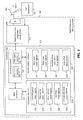
- FIG. 3 is a schematic block diagram of a RF transceiver for time aligning a plurality of RF signals in accordance with an embodiment of the present invention
- FIG. 4A is a timing diagram illustrating a plurality of sub-frames transmitted to a UE by a RF transceiver in accordance with an embodiment of the present invention
- FIG. 4B is a graph illustrating a plurality of values of a plurality of TA commands transmitted to the UE of FIG. 4A by the RF transceiver of FIG. 4A in accordance with an embodiment of the present invention.
- FIGS. 5A, 5B, 5C, 5D and 5E are a flow chart illustrating a method for aligning a time offset of a plurality of RF signals in accordance with an embodiment of the present invention.
- a radio-frequency (RF) transceiver in an RF communication network for aligning a time offset of a plurality of RF signals with a predetermined uplink timing of the RF transceiver.
- the RF signals are transmitted to the RF transceiver by a plurality of user equipments (UEs).
- the RF transceiver comprises first and second system memories and first and second processors.
- the first system memory stores a cool-off period value, a filter period value, a reset interval value, a first filter value, and a primary threshold value.
- the cool-off period value is indicative of a time required by at least one of the UEs to modify the time offset of the RF signals.
- the first processor retrieves the cool-off period value, the filter period value, the reset interval value, the first filter value, and the primary threshold value from the first system memory.
- the first processor receives a time offset value indicative of the time offset of the RF signals and generates a control signal indicative of transmission of the time offset value to the at least one UE.
- the second processor receives the cool-off period value, the filter period value, the reset interval value, the first filter value, and the primary threshold value from the first processor.
- the second processor further receives a digital baseband signal corresponding to the RF signals.
- the second processor generates a second filter value based on the first filter value and generates first and second threshold values based on the primary threshold value and a default time offset value.
- the second processor initializes a filter start counter for generating a filter length value and initializes a filter span counter when the filter length value exceeds the cool-off period value for generating a filter span value.
- the filter span value exceeds the filter period value after a first time period after initialization of the filter span counter.
- the filter span value exceeds the reset interval value after a second time period subsequent to the first time period.
- the second processor generates an instantaneous time offset value based on the digital baseband signal during the first and second time periods, modifies the time offset value based on the instantaneous time offset value and the first and second filter values during the first and second time periods, transmits the default time offset value as the time offset value to the first processor during the first time period, transmits the modified time offset value as the time offset value to the first processor based on the first and second threshold values during the second time period, receives the control signal from the first processor during the second time period, and transmits the modified time offset value to the at least one UE based on the control signal during the second time period. Further, the second processor resets the filter start and filter span counters and the modified time offset value after the second time period.
- a method for aligning a time offset of a plurality of RF signals with a predetermined uplink timing of an RF transceiver is provided.
- the RF signals are transmitted to the RF transceiver by a plurality of UEs.
- the RF transceiver includes first and second processors.
- the method includes receiving a cool-off period value, a filter period value, a reset interval value, a first filter value, a primary threshold value, and a digital baseband signal corresponding to the RF signals.
- the cool-off period value is indicative of a time required by at least one of the UEs to modify the time offset of the RF signals.
- the method further includes generating a second filter value based on the first filter value and generating first and second threshold values based on the primary threshold value and a default time offset value.
- a filter start counter is initialized for generating a filter length value and a filter span counter is initialized when the filter length value exceeds the value of the cool-off period for generating a filter span value.
- the filter span value exceeds the filter period value after a first time period and the filter span value exceeds the reset interval value after a second time period subsequent to the first time period.
- An instantaneous time offset value is generated based on the digital baseband signal during the first and second time periods.
- a time offset value is modified based on the instantaneous time offset value and the first and second filter values during the first and second time periods.
- the default time offset value is transmitted as the time offset value by the second processor to the first processor during the first time period.
- the modified time offset value is transmitted as the time offset value by the second processor to the first processor based on the first and second threshold values during the second time period.
- the method further includes receiving the time offset value indicative of the time offset of the RF signals at the first processor.
- a control signal indicative of transmission of the time offset value to the at least one UE is generated.
- the control signal is received at the second processor during the second time period.
- the modified time offset value is transmitted to the at least one UE.
- the filter start and filter span counters and the modified time offset value is reset after the second time period.
- Various embodiments of the present invention provide a radio-frequency (RF) transceiver in an RF communication network for aligning a time offset of a plurality of RF signals with a predetermined uplink timing of the RF transceiver.
- the RF signals are transmitted to the RF transceiver by a plurality of UEs.
- the first processor retrieves a cool-off period value, a filter period value, a reset interval value, a first filter value, and a primary threshold value from a first system memory.
- the cool-off period value is indicative of a time required by at least one of the UEs to modify the time offset of the plurality of RF signals.
- the first processor receives a time offset value indicative of the time offset of the plurality of RF signals and generates a control signal indicative of transmission of the time offset value to the at least one UE.
- the second processor receives a digital baseband signal corresponding to the plurality of RF signals, generates a second filter value based on the first filter value and generates first and second threshold values based on the primary threshold value and a default time offset value, and initializes a filter start counter for generating a filter length value and initializes a filter span counter when the filter length value exceeds the cool-off period value for generating a filter span value.
- the filter span value exceeds the filter period value after a first time period after the initialization of the filter span counter.
- the filter span value exceeds the value of the reset interval after a second time period subsequent to the first time period.
- the second processor generates an instantaneous time offset value based on the digital baseband signal during the first and second time periods, modifies the time offset value based on the instantaneous time offset value and the first and second filter values during the first and second time periods, transmits the default time offset value as the time offset value to the first processor during the first time period, transmits the modified time offset value as the time offset value to the first processor based on the first and second threshold values during the second time period, receives the control signal from the first processor during the second time period, and transmits the modified time offset value to the at least one UE based on the control signal during the second time period. Further, the second processor initializes the filter start counter after the resetting of the filter start and filter span counters at the end of the second time period. Subsequently, the filter length value exceeds the cool-off period value after a third time period that equals the cool-off value.
- the RF transceiver provides enough time to the UE to adjust the transmission time of the uplink RF signals in the third time period. Hence, a state of oscillation of the UE between misaligned start positions of the sub-frames caused due to transmission of multiple TA commands to the UE is avoided, thereby preventing misalignment of the RF signals received at the eNB and providing optimum throughput. Further, the RF transceiver facilitates an operator to store the cool-off period value, the filter period value, the reset interval value, and the primary threshold value, thereby providing the operator a control over the RF transceiver. Thus, the RF transceiver can be programmed by the operator to suit the requirements of the RF communication network.
- FIG. 3 a schematic block diagram of a RF transceiver 302 for aligning a time offset of a plurality of RF signals with a predetermined uplink timing (hereinafter referred to as predetermined uplink time offset) in accordance with an embodiment of the present invention is shown.
- the RF signals are transmitted by a UE 304 to the RF transceiver 302 .
- the RF transceiver 302 and the UE 304 are included in an RF communication network.
- the RF transceiver 302 is at least one of a macro-cell RF transceiver, a micro-cell RF transceiver, a pico-cell RF transceiver, and a femto-cell RF transceiver.
- the RF transceiver 302 is an eNode-B (or “eNB”) and the RF communication network is based on the LTE standard.
- the RF signals transmitted by the UE 304 to the RF transceiver 302 are hereinafter referred to as uplink RF signals.
- the time offset of the uplink RF signals is a time difference between a starting position of a sub-frame received by the UE 304 from the RF transceiver 302 and a starting position of a sub-frame transmitted to the RF transceiver 302 by the UE 304 .
- the RF transceiver 302 assigns a set of sub-frames at a set of RF sub-carrier frequencies to the UE 304 .
- the RF transceiver 302 is connected to an antenna 306 for transmitting and receiving the RF signals to and from the UE 304 , respectively.
- the RF transceiver 302 includes a power amplifier (PA) 308 , a radio-frequency integrated circuit (RFIC) 310 , and a baseband chip 312 .
- the baseband chip 312 includes first and second processors 314 and 316 and first and second system memories 318 and 320 .
- the antenna 306 transmits and receives the RF signals to and from the UE 304 , respectively.
- the antenna 306 is connected to the PA 308 and the RFIC 310 .
- the PA 308 receives the RF signals from the RFIC 310 .
- the PA 308 amplifies the RF signals, i.e., increases the amplitude of the RF signals and transmits the amplified RF signals to the antenna 306 .
- the antenna 306 then transmits the amplified RF signals to the UE 304 through free space.
- the antenna 306 receives the RF signals from the UE 304 through free space and transmits the RF signals to the RFIC 310 .
- the RFIC 310 generates a low-frequency signal based on the RF signals by way of a mixer (not shown).
- the RFIC 310 further generates a digital baseband signal based on the low-frequency signal by way of an analog-to-digital converter (ADC) (not shown).
- ADC analog-to-digital converter
- the digital baseband signal corresponds to the RF signals received from the UE 304 .
- the RFIC 310 transmits the digital baseband signal to the baseband chip 312 .
- the first system memory 318 includes a cool-off period value register 322 for storing a cool-off period value, a filter period value register 324 for storing a filter period value, a reset interval value register 326 for storing a reset interval value, a first filter value register 328 for storing a first filter value, and a primary threshold value register 330 for storing a primary threshold value.
- the cool-off period value is a time required by the UE 304 for modifying the time offset of the uplink RF signals.
- the first processor 314 is connected to the first system memory 318 and the second processor 316 .
- the first processor 314 retrieves and transmits the cool-off period value, the filter period value, the reset interval value, the first filter value, and the primary threshold value from the first system memory 318 to the second processor 316 .
- the first processor 314 performs layer 2 processing of a wireless protocol stack.
- the first processor 314 is an LTE layer 2 (L2) processor.
- L2 LTE layer 2
- the first processor 314 receives a time offset value from the second processor 316 .
- the first processor 314 enables an operator to store the cool-off period value, the filter period value, the reset interval value, the first filter value, and the primary threshold value in the cool-off period value register 322 , the filter period value register 324 , the reset interval value register 326 , the first filter value register 328 , and the primary threshold value register 330 , respectively.
- the first processor 314 executes software stored in the first system memory 318 .
- the software enables an operator to program the cool-off period value, the filter period value, the reset interval value, the first filter value, and the primary threshold value by executing the computer readable program code on the first processor 314 . Further, the software enables the operator to control the generation of time offset values transmitted to the UE 304 .
- the second system memory 320 is connected to the second processor 316 .
- the second system memory 320 includes a filter start count register 332 for storing a filter length value, a filter span count register 334 for storing a filter span value, an instantaneous time offset value register 336 for storing an instantaneous time offset value, and a time offset value register 338 for storing the time offset value.
- the second processor 316 includes a filter start counter 340 and a filter span counter 342 .
- the second processor 316 receives the cool-off period value, the filter period value, the reset interval value, the first filter value, and the primary threshold value from the first processor 314 and the digital baseband signal from the RFIC 310 .
- the second processor 316 performs layer 1 (L1) processing of the wireless protocol stack.
- the second processor 316 is an LTE L1 processor.
- the second processor 316 generates a second filter value based on the value of the first filter, and generates first and second threshold values based on the primary threshold value.
- the second processor 316 initializes the filter start counter 340 for generating the filter length value.
- the second processor 316 stores the filter length value in the filter start count register 332 .
- the second processor 316 increments the filter length value and stores the incremented filter length value in the filter start count register 332 .
- the second processor 316 monitors the filter length value and initializes the filter span counter 342 when the filter length value exceeds the cool-off period value.
- the filter span counter 342 generates the filter span value.
- the second processor 316 stores the filter span value in the filter span count register 334 .
- the second processor 316 increments the filter span value and stores the incremented filter span value in the filter span count register 334 .
- the incremented filter span value exceeds the filter period value after a first time period.
- the filter span value exceeds the reset interval value after a second time period subsequent to the first time period.
- the second processor 316 During the first time period, the second processor 316 generates the instantaneous time offset value based on the digital baseband signal corresponding to the uplink RF signals received from the UE 304 .
- the UE 304 transmits a reference RF signal to the RF transceiver 302 and the digital baseband signal corresponds to the reference RF signal transmitted by the UE 304 .
- the examples of the reference RF signals include a sounding reference signal (SRS) and a demodulation reference signal (DMRS).
- SRS sounding reference signal
- DMRS demodulation reference signal
- the second processor 316 generates and modifies the time offset value based on the instantaneous time offset value and the first and second filter values.
- the first and second filter values are indicative of first and second weights assigned to the time offset value and the instantaneous time offset value, respectively, for generating the modified time offset value.
- the second processor 316 overwrites the time offset value and stores the modified time offset value in the time offset value register 338 . However, during the first time period, the second processor 316 transmits a default time offset value to the first processor 314 .
- the default time offset value indicates that the uplink RF signals from the UE 304 are aligned to the predetermined uplink time offset computed by the RF transceiver 302 .
- the default time offset value is thirty-one.
- the time offset value greater than the default time offset value is indicative of advancement in the transmission time of the uplink RF signals.
- the time offset value less than the default time offset value is indicative of a delay in the transmission time of the uplink RF signals.
- each sub-frame has a time period of 1 msec.
- the second processor 316 receives the digital baseband signal from the RFIC 310 .
- the second processor 316 modifies the instantaneous time offset value based on the received digital baseband signal.
- the second processor 316 then stores the modified instantaneous time offset value in the instantaneous time offset value register 336 .
- the second processor 316 modifies the time offset value based on the instantaneous time offset value and the first and second filter values as shown in equation (4) and stores the modified time offset value in the time offset value register 338 .
- the second processor 316 checks to determine whether the modified time offset value is less than the first threshold value and greater than the second threshold value.
- the first and second threshold values are indicative of maximum and minimum values of the time offset value, respectively.
- the first threshold value is indicative of a maximum permitted advance in transmission time of the uplink RF signals transmitted by the UE 304 .
- the second threshold value is indicative of a maximum permitted delay in transmission time of the uplink RF signals transmitted by the UE 304 .
- the first and second threshold values collectively determine an allowable time offset window that restricts the modification range for the time offset of the transmission time of the uplink RF signals.
- the allowable time offset window includes a predefined set of time offset values.
- the time offset values transmitted to the UE 304 are confined to the time offset values within the allowable time offset window.
- the operator adjusts the allowable time offset window by configuring the primary threshold value stored in the primary threshold value register 330 .
- the second processor 316 determines that the modified time offset value is less than the first threshold value and greater than the second threshold value, the second processor 316 transmits the modified time offset as the time offset value to the first processor 314 . However, if the second processor 316 determines that the modified time offset value exceeds the first threshold value, the second processor 316 transmits the first threshold value as the time offset value to the first processor 314 . However, if the second processor 316 determines that the modified time offset value is less than the second threshold value, the second processor 316 transmits the second threshold value as the time offset value to the first processor 314 .
- the first processor 314 receives the time offset value and generates a control signal based on the time offset value.
- the control signal is indicative of transmission of the time offset value to the UE 304 .
- the control signal is indicative of the time offset value that is transmitted to the UE 304 by the RF transceiver 302 .
- the second processor 316 receives the control signal and transmits the time offset value to the UE 304 based on the control signal.
- the second processor 316 transmits the time offset value to the UE 304 in a time alignment (TA) command transmitted to the UE 304 .
- the TA command is transmitted to the UE 304 in a sub-frame on another downlink RF carrier signal during the second time period.
- TA time alignment
- the second processor 316 When the filter span value exceeds the reset interval value, the second processor 316 resets the filter start and filter span counters 340 and 342 and the modified time offset value.
- the second processor 316 resets the filter start and filter span counters 340 and 342 by storing a zero value in the filter start count register 332 and the filter span count register 334 . Further, the second processor 316 resets the time offset value by storing the default time offset value in the time offset value register 338 . Subsequently, the second processor 316 initializes the filter start counter 340 to generate the filter length value.
- the filter length value exceeds the cool-off period value after a third time period.
- the third time period equals the time required by the UE 304 to modify the time offset of the uplink RF signals. In an example, the third time period equals the cool-off period value.
- FIG. 4A a timing diagram illustrating a plurality of sub-frames transmitted to the UE 304 by the RF transceiver 302 in accordance with an embodiment of the present invention is shown.
- the UE 304 receives a first set of sub-frames 402 a in the time period T 0 -T 1 , a second set of sub-frames 402 b in the time period T 1 -T 2 , and a third set of sub-frames 402 c in the time period T 2 -T 3 .
- the UE 304 receives a fourth set of sub-frames 402 d in the time period T 3 -T 4 subsequent to receiving the third set of sub-frames 402 c in the time period T 2 -T 3 .
- the UE 304 receives a fifth set of sub-frames 402 e in the time period T 4 -T 5 subsequent to the time period T 3 -T 4 , and a sixth set of sub-frames 402 f in the time period T 5 -T 6 subsequent to the time period T 4 -T 5 .
- the time periods T 0 -T 1 and T 3 -T 4 correspond to the first time period.
- the time periods T 1 -T 2 and T 4 -T 5 correspond to the second time period.
- a first sub-frame (not shown) of the second set of sub-frames 402 b includes a first TA command 404 a and a second sub-frame (not shown) within the fifth set of sub-frames 402 e includes a second TA command 404 b.
- FIG. 4B a graph illustrating a plurality of values of the first and second TA commands 404 a and 404 b in accordance with an embodiment of the present invention is shown.
- the first and second TA commands 404 a and 404 b include value thirty-two.
- the first and second TA commands 404 a and 404 b correspond to the advancement in the transmission time of the uplink RF signals by a time interval corresponding to 1TA.
- the second processor 316 receives the reset interval value, the filter period value, the cool-off period value, the first filter value and the primary threshold value from the first processor 314 and the digital baseband signal from the RFIC 310 .
- the second processor 316 generates the second filter value based on the first filter value and generates the first and second threshold values based on the primary threshold value as shown in equations (1), (2), and (3), respectively.
- the second processor 316 initializes the filter start counter 340 to generate the filter length value.
- the filter length value exceeds the cool-off period value and the second processor 316 initializes the filter span counter 342 to generate the filter span value.
- the filter span value exceeds the filter period value after the time period T 0 -T 1 (hereinafter referred to as first time period T 0 -T 1 ).
- the second processor 316 During the first time period T 0 -T 1 , the second processor 316 generates the instantaneous time offset value based on the digital baseband signal. The second processor 316 then generates and modifies the time offset value based on the instantaneous time offset value and the first and second filter values as shown in equation (4). However, the second processor 316 transmits the default time offset value as the time offset value to the first processor 314 . Further, the second processor 316 transmits the first set of sub-frames 402 a to the UE 304 .
- the second processor 316 During the time period T 1 -T 2 (hereinafter referred to as second time period T 1 -T 2 ), the second processor 316 generates and modifies the instantaneous time offset value based on the digital baseband signal. The second processor 316 then modifies the time offset value based on the instantaneous time offset value and the first and second filter values as shown in equation (4). When the modified time offset value exceeds the first threshold value, the second processor 316 transmits the first threshold value as the time offset value to the first processor 314 . When the modified time offset value is less than the second threshold value, the second processor 316 transmits the second threshold value as the time offset value to the first processor 314 .
- the second processor 316 transits the modified time offset value as the time offset value to the first processor 314 .
- the filter span value exceeds the reset interval value after the second time period T 1 -T 2 .
- the first processor 314 receives at least one of the modified time offset and the first and second threshold values as the time offset value, generates the control signal based on the time offset value, and transmits the control signal to the second processor 316 .
- the second processor 316 receives the control signal and transmits the modified time offset value to the UE 304 in the first TA command 404 a .
- the filter span value exceeds the reset interval value and the second processor 316 resets the filter start counter 340 , the filter span counter 342 , and the modified time offset value and initializes the filter start counter 340 to generate the filter length value.
- the filter length value exceeds the cool-off period value.
- the RF transceiver 302 provides adequate time to the UE 304 to adjust the transmission time of the uplink RF signals during the time period T 2 -T 3 (hereinafter referred to as third time period T 2 -T 3 ) based on the first TA command 404 a , thereby avoiding a state of oscillation of the UE 304 between misaligned start positions of the sub-frame caused due to multiple TA commands transmitted in successive sub-frames.
- misalignment of the RF signals received at the eNB is prevented, thereby increasing the throughput of the eNB.
- the cool-off period value, the filter period value, the reset interval value, the first filter value, and the primary threshold value are programmable by the operator, thereby providing the operator a control over the generation and transmission of the first and second TA commands 404 a and 404 b .
- the software executed by the first processor 314 enables the operator to control time intervals of the first, second and third time periods, thereby providing flexibility to the operators to program the first processor 314 based on the requirements of the RF communication system.
- FIGS. 5A, 5B, 5C, and 5D a flow chart illustrating a method for aligning the time offset of the plurality of RF signals transmitted by the UE 304 to the RF transceiver 302 with the predetermined uplink time offset in accordance with an embodiment of the present invention is shown.
- the second processor 316 receives the cool-off period value, the filter period value, the reset interval value, the first filter value, and the primary threshold value from the first processor 314 and the digital baseband signal from the RFIC 310 .
- the second processor 316 initializes the filter start counter 340 for generating the filter length value.
- the second processor 316 increments the filter length value and stores the incremented filter length value in the filter start count register 332 .
- the second processor 316 compares the filter length value and the cool-off period value.
- the second processor 316 checks to determine whether the filter length value exceeds the cool-off period value.
- the second processor 316 determines that the filter length value does not exceed the cool-off period value. However, if at step 510 the second processor 316 determines that the filter length value exceeds the cool-off period value, the second processor 316 executes step 512 .
- the second processor 316 increments the filter length value and stores the incremented filter length value in the filter start count register 332 .
- the second processor 316 generates the first and second threshold values based on the primary threshold value as shown in equations (2) and (3).
- the second processor 316 generates the second filter value based on the first filter value as shown in equation (1).
- the second processor 316 initializes the filter span counter 342 for generating the filter span value.
- the second processor 316 increments the filter span value and stores the incremented filter span value in the filter span count register 334 .
- the second processor 316 compares the filter span value and the filter period value. The second processor 316 executes step 524 after executing step 522 .
- the second processor 316 checks to determine whether the filter span value exceeds the filter period value. If at step 524 , the second processor 316 determines that the filter span value does not exceed the filter period value, the second processor 316 executes step 532 . However, if at step 524 the second processor 316 determines that the filter span value exceeds the filter period value, the second processor 316 executes step 526 . At step 526 , the second processor 316 increments the filter span value and stores the incremented filter span value in the filter span count register 334 . At step 528 , the second processor 316 compares the filter span value and the reset interval value.
- the second processor 316 checks to determine whether the filter span value exceeds the reset interval value. If at step 530 the second processor 316 determines that the filter span value does not exceed the reset interval value, the second processor 316 executes step 540 . However, if at step 530 the second processor 316 determines that the filter span value exceeds the reset interval value, the second processor 316 executes step 556 .
- the second processor 316 generates the instantaneous time offset value based on the digital baseband signal.
- the second processor 316 generates and modifies the time offset value based on the instantaneous time offset value and the first and second filter values as shown in equation (4).
- the second processor 316 transmits the default time offset value as the time offset value to the first processor 314 .
- the second processor 316 increments the filter span value and stores the incremented filter span value in the filter span count register 334 .
- the second processor 316 executes step 522 after executing step 538 .
- the second processor 316 generates the instantaneous time offset value based on the digital baseband signal.
- the second processor 316 modifies the time offset value based on the instantaneous time offset value and the first and second filter values as shown in equation (4).
- the second processor 316 transmits the modified time offset value as the time offset value to the first processor 314 based on the first and second threshold values.
- the first processor 314 receives the time offset value.
- the first processor 314 generates the control signal based on the time offset value.
- the second processor 316 receives the control signal.
- the second processor 316 transmits the modified time offset value to the UE 304 based on the control signal.
- the second processor 316 increments the filter span value and stores the incremented filter span value in the filter span count register 334 .
- the second processor 316 executes step 528 after executing step 554 .
- the second processor 316 resets the filter start and filter span counters 340 and 342 , respectively, and the modified time offset value.
- the second processor 316 checks to determine whether any more digital baseband signals are expected to be received. If at step 558 , the second processor 316 determines that there are more digital baseband signals to be received, the second processor 316 executes step 504 .
- the RF transceiver 302 expects to receive more digital baseband signals when the RF transceiver 302 is in a working state and the RF transceiver 302 does not expect to receive more digital baseband signals when the RF transceiver 302 is in a standby state. In another embodiment, the RF transceiver 302 does not expect to receive more digital baseband signals when the RF transceiver 302 is switched off.
Abstract
Description
Second filter value=1−first filter value (1)
The
First threshold value=default time offset value+primary threshold value (2)
Further, the
Second threshold value=default time offset value−primary threshold value (3)
Modified time offset value=(time offset value*first filter value)+(instantaneous time offset value*second filter value) (4)
Claims (20)
Priority Applications (1)
| Application Number | Priority Date | Filing Date | Title |
|---|---|---|---|
| US14/681,047 US9491758B2 (en) | 2015-04-07 | 2015-04-07 | System for alignment of RF signals |
Applications Claiming Priority (1)
| Application Number | Priority Date | Filing Date | Title |
|---|---|---|---|
| US14/681,047 US9491758B2 (en) | 2015-04-07 | 2015-04-07 | System for alignment of RF signals |
Publications (2)
| Publication Number | Publication Date |
|---|---|
| US20160302194A1 US20160302194A1 (en) | 2016-10-13 |
| US9491758B2 true US9491758B2 (en) | 2016-11-08 |
Family
ID=57112024
Family Applications (1)
| Application Number | Title | Priority Date | Filing Date |
|---|---|---|---|
| US14/681,047 Expired - Fee Related US9491758B2 (en) | 2015-04-07 | 2015-04-07 | System for alignment of RF signals |
Country Status (1)
| Country | Link |
|---|---|
| US (1) | US9491758B2 (en) |
Families Citing this family (3)
| Publication number | Priority date | Publication date | Assignee | Title |
|---|---|---|---|---|
| US10122500B2 (en) * | 2015-08-26 | 2018-11-06 | Apple Inc. | Efficient sparse network resource usage and connection release |
| US20210345278A1 (en) | 2018-10-16 | 2021-11-04 | Ntt Docomo, Inc. | Terminal and communication method |
| US11395242B2 (en) * | 2019-02-01 | 2022-07-19 | Cisco Technology, Inc. | Link establishment between a radio equipment controller (REC) and radio equipment (RE) in a fronthaul network |
Citations (20)
| Publication number | Priority date | Publication date | Assignee | Title |
|---|---|---|---|---|
| US5657358A (en) * | 1985-03-20 | 1997-08-12 | Interdigital Technology Corporation | Subscriber RF telephone system for providing multiple speech and/or data signals simultaneously over either a single or plurality of RF channels |
| US5745777A (en) * | 1994-05-10 | 1998-04-28 | Seiko Communications Holding N.V. | Analyzer for frequency modulated signals |
| US20060120441A1 (en) * | 2004-12-02 | 2006-06-08 | Renesas Technology Corp. | Receiver |
| US20070129034A1 (en) * | 2003-07-17 | 2007-06-07 | Adams Andrew R | Adaptive agc in a wireless network receiver |
| US20070149206A1 (en) | 2005-12-22 | 2007-06-28 | Interdigital Technology Corporation | Method and system for adjusting uplink transmission timing for long term evolution handover |
| US20070178875A1 (en) * | 2005-06-28 | 2007-08-02 | Rao Anil S | Systems, methods, and apparatus for activity control in a wireless communications device |
| US20090168939A1 (en) * | 2007-12-31 | 2009-07-02 | Silicon Laboratories Inc. | Hardware synchronizer for 802.15.4 radio to minimize processing power consumption |
| US20090168848A1 (en) * | 2007-12-31 | 2009-07-02 | Silicon Laboratories Inc. | Single chip low power fully integrated 802.15.4 radio platform |
| US20100061361A1 (en) | 2008-09-09 | 2010-03-11 | Chih-Hsiang Wu | Methods utilized in mobile device for handling situations when time alignment timer expires, and mobile device thereof |
| US20100171659A1 (en) * | 2008-10-02 | 2010-07-08 | Texas Instruments Incorporated | Position engine (pe) feedback to improve gnss receiver performance |
| US20110102258A1 (en) * | 2003-09-02 | 2011-05-05 | Sirf Technology, Inc. | Signal Processing System for Satellite Positioning Signals |
| US20110223932A1 (en) | 2010-03-12 | 2011-09-15 | David Philip Hole | Timing advance enhancements for cellular communications |
| US8081942B1 (en) * | 2007-05-14 | 2011-12-20 | Marvell International Ltd. | Method and apparatus for muting based on a constant modulus indication |
| US20120014371A1 (en) | 2010-07-16 | 2012-01-19 | Research In Motion Limited | Method and apparatus for autonomous uplink timing advance maintenance |
| US8325865B1 (en) * | 2011-07-31 | 2012-12-04 | Broadcom Corporation | Discrete digital receiver |
| US20120313817A1 (en) * | 2003-09-02 | 2012-12-13 | Csr Technology Inc. | Signal processing system for satellite positioning signals |
| US20130258959A1 (en) | 2012-04-01 | 2013-10-03 | Esmael Hejazi Dinan | Uplink Transmission Timing Advance in a Wireless Device and Base Station |
| US8718102B2 (en) | 2011-12-15 | 2014-05-06 | Intel Corporation | Minimalistic LTE maintenance timing advance method |
| US20140270024A1 (en) | 2013-03-14 | 2014-09-18 | Nokia Corporation | Apparatus and method for detection of time tracking failure |
| US9112471B1 (en) * | 2014-03-19 | 2015-08-18 | Freescale Semiconductor, Inc. | Gain control system for wireless communication system |
-
2015
- 2015-04-07 US US14/681,047 patent/US9491758B2/en not_active Expired - Fee Related
Patent Citations (20)
| Publication number | Priority date | Publication date | Assignee | Title |
|---|---|---|---|---|
| US5657358A (en) * | 1985-03-20 | 1997-08-12 | Interdigital Technology Corporation | Subscriber RF telephone system for providing multiple speech and/or data signals simultaneously over either a single or plurality of RF channels |
| US5745777A (en) * | 1994-05-10 | 1998-04-28 | Seiko Communications Holding N.V. | Analyzer for frequency modulated signals |
| US20070129034A1 (en) * | 2003-07-17 | 2007-06-07 | Adams Andrew R | Adaptive agc in a wireless network receiver |
| US20120313817A1 (en) * | 2003-09-02 | 2012-12-13 | Csr Technology Inc. | Signal processing system for satellite positioning signals |
| US20110102258A1 (en) * | 2003-09-02 | 2011-05-05 | Sirf Technology, Inc. | Signal Processing System for Satellite Positioning Signals |
| US20060120441A1 (en) * | 2004-12-02 | 2006-06-08 | Renesas Technology Corp. | Receiver |
| US20070178875A1 (en) * | 2005-06-28 | 2007-08-02 | Rao Anil S | Systems, methods, and apparatus for activity control in a wireless communications device |
| US20070149206A1 (en) | 2005-12-22 | 2007-06-28 | Interdigital Technology Corporation | Method and system for adjusting uplink transmission timing for long term evolution handover |
| US8081942B1 (en) * | 2007-05-14 | 2011-12-20 | Marvell International Ltd. | Method and apparatus for muting based on a constant modulus indication |
| US20090168939A1 (en) * | 2007-12-31 | 2009-07-02 | Silicon Laboratories Inc. | Hardware synchronizer for 802.15.4 radio to minimize processing power consumption |
| US20090168848A1 (en) * | 2007-12-31 | 2009-07-02 | Silicon Laboratories Inc. | Single chip low power fully integrated 802.15.4 radio platform |
| US20100061361A1 (en) | 2008-09-09 | 2010-03-11 | Chih-Hsiang Wu | Methods utilized in mobile device for handling situations when time alignment timer expires, and mobile device thereof |
| US20100171659A1 (en) * | 2008-10-02 | 2010-07-08 | Texas Instruments Incorporated | Position engine (pe) feedback to improve gnss receiver performance |
| US20110223932A1 (en) | 2010-03-12 | 2011-09-15 | David Philip Hole | Timing advance enhancements for cellular communications |
| US20120014371A1 (en) | 2010-07-16 | 2012-01-19 | Research In Motion Limited | Method and apparatus for autonomous uplink timing advance maintenance |
| US8325865B1 (en) * | 2011-07-31 | 2012-12-04 | Broadcom Corporation | Discrete digital receiver |
| US8718102B2 (en) | 2011-12-15 | 2014-05-06 | Intel Corporation | Minimalistic LTE maintenance timing advance method |
| US20130258959A1 (en) | 2012-04-01 | 2013-10-03 | Esmael Hejazi Dinan | Uplink Transmission Timing Advance in a Wireless Device and Base Station |
| US20140270024A1 (en) | 2013-03-14 | 2014-09-18 | Nokia Corporation | Apparatus and method for detection of time tracking failure |
| US9112471B1 (en) * | 2014-03-19 | 2015-08-18 | Freescale Semiconductor, Inc. | Gain control system for wireless communication system |
Also Published As
| Publication number | Publication date |
|---|---|
| US20160302194A1 (en) | 2016-10-13 |
Similar Documents
| Publication | Publication Date | Title |
|---|---|---|
| US11647472B2 (en) | Timing and frame structure in an integrated access backhaul (IAB) network | |
| US20230057591A1 (en) | Autonomous timing adjustment for a wireless device | |
| US20220369238A1 (en) | Uplink power control for srs carrier-based switching | |
| EP3143809B1 (en) | Handling of cells associated with timing advance groups in a wireless communications system | |
| WO2016045620A1 (en) | Device, network, and method for communications with variable-duration reference signals | |
| EP2963989A1 (en) | LTE transmission in unlicensed bands | |
| US20130196707A1 (en) | User Equipment, Network Node and Methods Therein | |
| EP3353940B1 (en) | Communication terminal, system node and methods therein | |
| US10827427B2 (en) | On/off time mask for short TTI | |
| US10165455B2 (en) | Coordination for PBCH | |
| US10057894B2 (en) | Base station, terminal, and communication system | |
| KR20220033525A (en) | Node for a radio communication network and operating method | |
| WO2018164809A1 (en) | Method and apparatus for uplink power headroom reporting | |
| WO2017061939A1 (en) | Wireless device, network node and methods performed therein | |
| US20230239126A1 (en) | Apparatus and Methods for Secondary Cell (SCell) Enhancements in Wireless Communications | |
| US9491758B2 (en) | System for alignment of RF signals | |
| EP3642992A1 (en) | Adaptation of on/off mask for nr with different numerologies | |
| EP2903356B1 (en) | Network node and method therein | |
| WO2019232726A1 (en) | Methods, device and computer-readable medium for determining timing advance | |
| OA20331A (en) | On/Off time mask for short TTI. |
Legal Events
| Date | Code | Title | Description |
|---|---|---|---|
| AS | Assignment |
Owner name: FREESCALE SEMICONDUCTOR,INC, TEXAS Free format text: ASSIGNMENT OF ASSIGNORS INTEREST;ASSIGNORS:SHARMA, AJAY;CHARIPADI, GOPIKRISHNA;PARUCHURI, LOKSIVA;SIGNING DATES FROM 20150406 TO 20150407;REEL/FRAME:035352/0774 |
|
| AS | Assignment |
Owner name: CITIBANK, N.A., AS NOTES COLLATERAL AGENT, NEW YORK Free format text: SUPPLEMENT TO IP SECURITY AGREEMENT;ASSIGNOR:FREESCALE SEMICONDUCTOR, INC.;REEL/FRAME:036284/0339 Effective date: 20150724 Owner name: CITIBANK, N.A., AS NOTES COLLATERAL AGENT, NEW YORK Free format text: SUPPLEMENT TO IP SECURITY AGREEMENT;ASSIGNOR:FREESCALE SEMICONDUCTOR, INC.;REEL/FRAME:036284/0105 Effective date: 20150724 Owner name: CITIBANK, N.A., AS NOTES COLLATERAL AGENT, NEW YORK Free format text: SUPPLEMENT TO IP SECURITY AGREEMENT;ASSIGNOR:FREESCALE SEMICONDUCTOR, INC.;REEL/FRAME:036284/0363 Effective date: 20150724 Owner name: CITIBANK, N.A., AS NOTES COLLATERAL AGENT, NEW YOR Free format text: SUPPLEMENT TO IP SECURITY AGREEMENT;ASSIGNOR:FREESCALE SEMICONDUCTOR, INC.;REEL/FRAME:036284/0339 Effective date: 20150724 Owner name: CITIBANK, N.A., AS NOTES COLLATERAL AGENT, NEW YOR Free format text: SUPPLEMENT TO IP SECURITY AGREEMENT;ASSIGNOR:FREESCALE SEMICONDUCTOR, INC.;REEL/FRAME:036284/0363 Effective date: 20150724 Owner name: CITIBANK, N.A., AS NOTES COLLATERAL AGENT, NEW YOR Free format text: SUPPLEMENT TO IP SECURITY AGREEMENT;ASSIGNOR:FREESCALE SEMICONDUCTOR, INC.;REEL/FRAME:036284/0105 Effective date: 20150724 |
|
| AS | Assignment |
Owner name: FREESCALE SEMICONDUCTOR, INC., TEXAS Free format text: PATENT RELEASE;ASSIGNOR:CITIBANK, N.A., AS COLLATERAL AGENT;REEL/FRAME:037357/0859 Effective date: 20151207 |
|
| AS | Assignment |
Owner name: MORGAN STANLEY SENIOR FUNDING, INC., MARYLAND Free format text: ASSIGNMENT AND ASSUMPTION OF SECURITY INTEREST IN PATENTS;ASSIGNOR:CITIBANK, N.A.;REEL/FRAME:037565/0527 Effective date: 20151207 Owner name: MORGAN STANLEY SENIOR FUNDING, INC., MARYLAND Free format text: ASSIGNMENT AND ASSUMPTION OF SECURITY INTEREST IN PATENTS;ASSIGNOR:CITIBANK, N.A.;REEL/FRAME:037565/0510 Effective date: 20151207 |
|
| AS | Assignment |
Owner name: MORGAN STANLEY SENIOR FUNDING, INC., MARYLAND Free format text: SUPPLEMENT TO THE SECURITY AGREEMENT;ASSIGNOR:FREESCALE SEMICONDUCTOR, INC.;REEL/FRAME:039138/0001 Effective date: 20160525 |
|
| AS | Assignment |
Owner name: NXP, B.V., F/K/A FREESCALE SEMICONDUCTOR, INC., NETHERLANDS Free format text: RELEASE BY SECURED PARTY;ASSIGNOR:MORGAN STANLEY SENIOR FUNDING, INC.;REEL/FRAME:040925/0001 Effective date: 20160912 Owner name: NXP, B.V., F/K/A FREESCALE SEMICONDUCTOR, INC., NE Free format text: RELEASE BY SECURED PARTY;ASSIGNOR:MORGAN STANLEY SENIOR FUNDING, INC.;REEL/FRAME:040925/0001 Effective date: 20160912 |
|
| STCF | Information on status: patent grant |
Free format text: PATENTED CASE |
|
| AS | Assignment |
Owner name: NXP B.V., NETHERLANDS Free format text: RELEASE BY SECURED PARTY;ASSIGNOR:MORGAN STANLEY SENIOR FUNDING, INC.;REEL/FRAME:040928/0001 Effective date: 20160622 |
|
| AS | Assignment |
Owner name: NXP USA, INC., TEXAS Free format text: MERGER;ASSIGNOR:FREESCALE SEMICONDUCTOR, INC.;REEL/FRAME:041144/0363 Effective date: 20161107 |
|
| AS | Assignment |
Owner name: NXP B.V., NETHERLANDS Free format text: RELEASE BY SECURED PARTY;ASSIGNOR:MORGAN STANLEY SENIOR FUNDING, INC.;REEL/FRAME:050744/0097 Effective date: 20190903 |
|
| AS | Assignment |
Owner name: NXP B.V., NETHERLANDS Free format text: CORRECTIVE ASSIGNMENT TO CORRECT THE REMOVEAPPLICATION 11759915 AND REPLACE IT WITH APPLICATION11759935 PREVIOUSLY RECORDED ON REEL 040928 FRAME 0001. ASSIGNOR(S) HEREBY CONFIRMS THE RELEASE OF SECURITYINTEREST;ASSIGNOR:MORGAN STANLEY SENIOR FUNDING, INC.;REEL/FRAME:052915/0001 Effective date: 20160622 |
|
| AS | Assignment |
Owner name: NXP, B.V. F/K/A FREESCALE SEMICONDUCTOR, INC., NETHERLANDS Free format text: CORRECTIVE ASSIGNMENT TO CORRECT THE REMOVEAPPLICATION 11759915 AND REPLACE IT WITH APPLICATION11759935 PREVIOUSLY RECORDED ON REEL 040925 FRAME 0001. ASSIGNOR(S) HEREBY CONFIRMS THE RELEASE OF SECURITYINTEREST;ASSIGNOR:MORGAN STANLEY SENIOR FUNDING, INC.;REEL/FRAME:052917/0001 Effective date: 20160912 |
|
| FEPP | Fee payment procedure |
Free format text: MAINTENANCE FEE REMINDER MAILED (ORIGINAL EVENT CODE: REM.); ENTITY STATUS OF PATENT OWNER: LARGE ENTITY |
|
| LAPS | Lapse for failure to pay maintenance fees |
Free format text: PATENT EXPIRED FOR FAILURE TO PAY MAINTENANCE FEES (ORIGINAL EVENT CODE: EXP.); ENTITY STATUS OF PATENT OWNER: LARGE ENTITY |
|
| STCH | Information on status: patent discontinuation |
Free format text: PATENT EXPIRED DUE TO NONPAYMENT OF MAINTENANCE FEES UNDER 37 CFR 1.362 |
|
| FP | Lapsed due to failure to pay maintenance fee |
Effective date: 20201108 |