US9491432B2 - Video processing apparatus for generating video output satisfying display capability of display device according to video input and related method thereof - Google Patents
Video processing apparatus for generating video output satisfying display capability of display device according to video input and related method thereof Download PDFInfo
- Publication number
- US9491432B2 US9491432B2 US12/814,515 US81451510A US9491432B2 US 9491432 B2 US9491432 B2 US 9491432B2 US 81451510 A US81451510 A US 81451510A US 9491432 B2 US9491432 B2 US 9491432B2
- Authority
- US
- United States
- Prior art keywords
- video
- data
- format
- input
- picture
- Prior art date
- Legal status (The legal status is an assumption and is not a legal conclusion. Google has not performed a legal analysis and makes no representation as to the accuracy of the status listed.)
- Expired - Fee Related, expires
Links
Images


Classifications
-
- H04N13/0029—
-
- H—ELECTRICITY
- H04—ELECTRIC COMMUNICATION TECHNIQUE
- H04N—PICTORIAL COMMUNICATION, e.g. TELEVISION
- H04N13/00—Stereoscopic video systems; Multi-view video systems; Details thereof
- H04N13/10—Processing, recording or transmission of stereoscopic or multi-view image signals
- H04N13/106—Processing image signals
- H04N13/139—Format conversion, e.g. of frame-rate or size
-
- H04N13/0048—
-
- H—ELECTRICITY
- H04—ELECTRIC COMMUNICATION TECHNIQUE
- H04N—PICTORIAL COMMUNICATION, e.g. TELEVISION
- H04N13/00—Stereoscopic video systems; Multi-view video systems; Details thereof
- H04N13/10—Processing, recording or transmission of stereoscopic or multi-view image signals
- H04N13/106—Processing image signals
- H04N13/161—Encoding, multiplexing or demultiplexing different image signal components
-
- H04N13/026—
-
- H—ELECTRICITY
- H04—ELECTRIC COMMUNICATION TECHNIQUE
- H04N—PICTORIAL COMMUNICATION, e.g. TELEVISION
- H04N13/00—Stereoscopic video systems; Multi-view video systems; Details thereof
- H04N13/20—Image signal generators
- H04N13/261—Image signal generators with monoscopic-to-stereoscopic image conversion
-
- H—ELECTRICITY
- H04—ELECTRIC COMMUNICATION TECHNIQUE
- H04N—PICTORIAL COMMUNICATION, e.g. TELEVISION
- H04N2213/00—Details of stereoscopic systems
- H04N2213/007—Aspects relating to detection of stereoscopic image format, e.g. for adaptation to the display format
Definitions
- the disclosed embodiments of the present invention relate to displaying video contents on a display device, and more particularly, to a video processing apparatus for generating a video output satisfying the display capability of a display device according to a video input and related method thereof.
- Three-dimensional (3D) video presentation technology is developed to improve the viewing entertainment of the end-users.
- 3D glasses and 3D display devices are devised to realize the playback of the 3D video content.
- the 3D video content may be recorded using a full resolution scheme which transmits left-eye pictures and right-eye pictures by different bitstreams or may be recorded using a half resolution scheme which transmits a left-eye picture and a right-eye picture in each frame of a single bitstream.
- the 3D video content may be recorded using a frame/field sequential format, a side-by-side format, a line-by-line format, a top-and-bottom format, or a checker sampling format when either of the full resolution scheme and the half resolution scheme is employed.
- a 3D display device is available and supports a display video format such as one of the aforementioned 3D video formats, but the video bitstream provided from a video source complies with a source video format such as the other of the aforementioned 3D video formats.
- the 3D display device fails to properly display the 3D video content transmitted by the video bitstream when driven by a video output device according to a video output with the source video format. Consequently, there is no 3D effect perceived by the user though the video source can provide the 3D video content.
- a video processing apparatus for generating a video output satisfying the display capability of a display device according to a video input and related method thereof are proposed to solve the above-mentioned problem.
- an exemplary video processing apparatus includes a video decoder, a storage device, and a video output device.
- the video decoder decodes an encoded video input to generate a video input with a source video format.
- the storage device is coupled to the video decoder, and buffers the video input generated from the video decoder.
- the video output device is coupled to the storage device, and outputs a video output to a display device according to the video input buffered in the storage device.
- the video output has a display video format satisfying a display capability of the display device, and the source video format and the display video format are three-dimensional (3D) video formats different from each other.
- an exemplary video processing method includes the following steps: decoding an encoded video input to generate a video input with a source video format; buffering the video input generated from the video decoder; and outputting a video output to a display device according to the buffered video input.
- the video output has a display video format satisfying a display capability of the display device, and the source video format and the display video format are three-dimensional (3D) video formats different from each other.
- an exemplary video processing apparatus includes a video decoder, a first storage device, a storage control device, and a video output device.
- the video decoder decodes an encoded video input to generate a first video input with a source video format.
- the storage control device is coupled between the video decoder and the first storage device, and generates a second video input with a display video format to the first storage device according to the first video input with the source video format.
- the video output device is coupled to the first storage device, and outputs a video output to a display device according to the second video input buffered in the first storage device.
- the video output has the display video format satisfying a display capability of the display device, and the source video format and the display video format are three-dimensional (3D) video formats different from each other
- an exemplary video processing method includes the following steps: decoding an encoded video input to generate a first video input with a source video format; generating a second video input with a display video format to a first storage device according to the first video input with the source video format; and outputting a video output to a display device according to the second video input buffered in the first storage device.
- the video output has the display video format satisfying a display capability of the display device, and the source video format and the display video format are three-dimensional (3D) video formats different from each other.
- FIG. 1 is a diagram illustrating a video processing apparatus according to a first exemplary embodiment of the present invention.
- FIG. 2 is a diagram illustrating a first playback scenario of a video input.
- FIG. 3 is a diagram illustrating a second playback scenario of the video input.
- FIG. 4 is a diagram illustrating the storage arrangement for the video input with the frame/field sequential format.
- FIG. 5 is a diagram illustrating the storage arrangement for the video input with the top-and-bottom format.
- FIG. 6 is a diagram illustrating the storage arrangement for the video input with the side-by-side format.
- FIG. 7 is a diagram illustrating the storage arrangement for the video input with the line-by-line format.
- FIG. 8 is a diagram illustrating a first exemplary implementation of the video output device shown in FIG. 1 .
- FIG. 9 is a diagram illustrating a second exemplary implementation of the video output device shown in FIG. 1 .
- FIG. 10 is a diagram illustrating an exemplary data scanning operation for generating the video output with the frame/field sequential format according to the video input with the frame/field sequential format.
- FIG. 11 is a diagram illustrating an exemplary data scanning operation for generating the video output with the top-and-bottom format according to the video input with the frame/field sequential format.
- FIG. 12 is a diagram illustrating an exemplary data scanning operation for generating the video output with the side-by-side format according to the video input with the frame/field sequential format.
- FIG. 13 is a diagram illustrating an exemplary data scanning operation for generating the video output with the line-by-line format according to the video input with the frame/field sequential format.
- FIG. 14 is a diagram illustrating an exemplary data scanning operation for generating the video output with the frame/field sequential format according to the video input with the top-and-bottom format.
- FIG. 15 is a diagram illustrating an exemplary data scanning operation for generating the video output with the top-and-bottom format according to the video input with the top-and-bottom format.
- FIG. 16 is a diagram illustrating an exemplary data scanning operation for generating the video output with the side-by-side format according to the video input with the top-and-bottom format.
- FIG. 17 is a diagram illustrating an exemplary data scanning operation for generating the video output with the line-by-line format according to the video input with the top-and-bottom format.
- FIG. 18 is a diagram illustrating an exemplary data scanning operation for generating the video output with the frame/field sequential format according to the video input with the side-by-side format.
- FIG. 19 is a diagram illustrating an exemplary data scanning operation for generating the video output with the top-and-bottom format according to the video input with the side-by-side format.
- FIG. 20 is a diagram illustrating an exemplary data scanning operation for generating the video output with the side-by-side format according to the video input with the side-by-side format.
- FIG. 21 is a diagram illustrating an exemplary data scanning operation for generating the video output with the line-by-line format according to the video input with the side-by-side format.
- FIG. 22 is a diagram illustrating an exemplary data scanning operation for generating the video output with the frame/field sequential format according to the video input with the line-by-line format.
- FIG. 23 is a diagram illustrating an exemplary data scanning operation for generating the video output with the top-and-bottom format according to the video input with the line-by-line format.
- FIG. 24 is a diagram illustrating an exemplary data scanning operation for generating the video output with the side-by-side format according to the video input with the line-by-line format.
- FIG. 25 is a diagram illustrating an exemplary data scanning operation for generating the video output with the line-by-line format according to the video input with the line-by-line format.
- FIG. 26 is a diagram illustrating an exemplary data scanning operation for generating the video output with the checker sampling format according to the video input with the frame/field sequential format.
- FIG. 27 is a diagram illustrating an exemplary data scanning operation for generating the video output with the checker sampling format according to the video input with the top-and-bottom format.
- FIG. 28 is a diagram illustrating an exemplary data scanning operation for generating the video output with the checker sampling format according to the video input with the side-by-side format.
- FIG. 29 is a diagram illustrating an exemplary data scanning operation for generating the video output with the checker sampling format according to the video input with the line-by-line format.
- FIG. 30 is a diagram illustrating an exemplary data scanning operation for generating the video output with the checker sampling format according to the video input with the checker sampling format.
- FIG. 31 is a diagram illustrating an exemplary data scanning operation for generating the video output with the frame/field sequential format according to the video input with the checker sampling format.
- FIG. 32 is a diagram illustrating an exemplary data scanning operation for generating the video output with the top-and-bottom format according to the video input with the checker sampling format.
- FIG. 33 is a diagram illustrating an exemplary data scanning operation for generating the video output with the side-by-side format according to the video input with the checker sampling format.
- FIG. 34 is a diagram illustrating an exemplary data scanning operation for generating the video output with the line-by-line format according to the video input with the checker sampling format.
- FIG. 35 is a diagram illustrating a video processing apparatus according to a second exemplary embodiment of the present invention.
- FIG. 36 is a diagram illustrating a first operational scenario of generating another video input according to one video input generated from a video decoder.
- FIG. 37 is a diagram illustrating a second operational scenario of generating another video input according to one video input generated from a video decoder.
- FIG. 38 is a diagram illustrating a video processing apparatus according to a third exemplary embodiment of the present invention.
- FIG. 39 is a diagram illustrating an exemplary data scanning operation for generating the video output with the checker sampling format according to the video input with the frame/field sequential format.
- FIG. 40 is a diagram illustrating another exemplary data scanning operation for generating the video output with the checker sampling format according to the video input with the frame/field sequential format.
- FIG. 41 is a diagram illustrating an exemplary data scanning operation for generating the video output with the checker sampling format according to the video input with the top-and-bottom format.
- FIG. 42 is a diagram illustrating another exemplary data scanning operation for generating the video output with the checker sampling format according to the video input with the top-and-bottom format.
- FIG. 43 is a diagram illustrating an exemplary data scanning operation for generating the video output with the checker sampling format according to the video input with the side-by-side format.
- FIG. 44 is a diagram illustrating another exemplary data scanning operation for generating the video output with the checker sampling format according to the video input with the side-by-side format.
- FIG. 45 is a diagram illustrating an exemplary data scanning operation for generating the video output with the checker sampling format according to the video input with the line-by-line format.
- FIG. 46 is a diagram illustrating another exemplary data scanning operation for generating the video output with the checker sampling format according to the video input with the line-by-line format.
- the conception of the present invention is to perform a video format conversion for generating a video output satisfying the display capability of a display device when a source video format of a video input is different from a display video format supported by the display device.
- the required video format conversion may be accomplished by a video output device which is used to generate the video input to the display device, or accomplished by a storage control device disposed between a preceding video decoder and a following display output device.
- an optimized display quality of the video playback e.g., 3D video playback
- the source video format of the video input may be one of the frame/field sequential format, the side-by-side format, the line-by-line format, the top-and-bottom format, and the checker sampling format due to the full resolution scheme or the half resolution scheme
- the display video format supported by the display device may be one of the frame/field sequential format, the side-by-side format, the line-by-line format, the top-and-bottom format, and the checker sampling format due to the full resolution scheme or the half resolution scheme.
- FIG. 1 is a diagram illustrating a video processing apparatus according to a first exemplary embodiment of the present invention.
- the exemplary video processing apparatus 100 includes, but is not limited to, a video decoder 102 , a storage device 104 , and a video output device 106 .
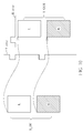
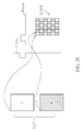
- a video input S_IN′ is generated from the video decoder 102 which decodes an encoded video input S_IN provided by a video source 110 such as an optical disc.
- the encoded video input S_IN provided by the video source 110 has encoded pictures
- the video input S_IN′ generated from the video decoder 102 contains reconstructed/decoded pictures to be displayed.
- the video input S_IN′ derived from decoding the encoded video input S_IN has a source video format VF_S.
- the storage device 104 may be implemented using a dynamic random access memory (DRAM), and is used to buffer the video input S_IN′ generated from the video decoder 102 .
- the video output device 106 is coupled to the storage device 104 , and is implemented for outputting a video output S_OUT to a display device (e.g., a 3D display device) 130 according to the video input S_IN′ buffered in the storage device 104 .
- a display device e.g., a 3D display device
- the video processing apparatus 100 may be disposed in a video playback device (e.g., an optical disc player or a set-top box) external to the display device 130 , and the video processing apparatus 100 is therefore coupled to the display device 130 through a connection cable such as a high-definition multimedia interface (HDMI) cable.
- a connection cable such as a high-definition multimedia interface (HDMI) cable.
- HDMI high-definition multimedia interface
- FIG. 2 is a diagram illustrating a first playback scenario of the video input S_IN′.
- the video input S_IN′ is a 3D video with the source video format VF_S
- the display device 130 is a 3D display device supporting the display video format VF_D identical to the source video format VF_S
- the video output device 106 is blocked from performing any video format conversion upon the video input S_IN′. Therefore, the video input S_IN′ is bypassed and directly serves as the video output S_OUT transmitted to the display device 130 which is a 3D display device.
- the video input S_IN′ which is a 3D video may have a video format being one of a plurality of 3D video formats including the frame/field sequential format, the side-by-side format, the line-by-line format, the top-and-bottom format, and the checker sampling format.
- the display device 130 which is a 3D display device may be configured to support a video format being one of the above-mentioned 3D video formats. If the 3D video format of the video input S_IN′ is identical to the 3D video format supported by the display device 130 , no format conversion from one 3D video format to another 3D video format is required, as shown in FIG. 2 .
- the 3D video format of the video input S_IN′ is not identical to the 3D video format supported by the display device 130 , a format conversion from one 3D video format to another 3D video format is necessitated for normal video content playback.
- FIG. 3 is a diagram illustrating a second playback scenario of the video input S_IN′.
- the video input S_IN′ is a 3D video with the source video format VF_S
- the display device 130 is a 3D display device supporting the display video format VF_D different from the source video format VF_S
- the video output device 106 therefore enables a 3D-to-3D conversion for processing the video input S_IN′ with the source video format VF_S to generate a 3D video with the display video format VF_D, wherein the generated 3D video serves as the video output S_OUT transmitted to the display device 130 which is a 3D display device.
- the video output device 106 when the video input S_IN′ has the source video format VF_S different from the display video format VF_D supported by the display device 130 (e.g., the source video format VF_S and the display video format VF_D are 3D video formats different from each other), the video output device 106 generates and outputs the video output S_OUT with the display video format VF_D satisfying the display capability of the display device 130 .
- the output of the display device 130 allows the viewer to have the 3D viewing experience though the original video input S_IN′ has a video format not complying with the display capability of the display device 130 .
- the video output device 106 has to receive data of the video input S_IN′ which is a 3D video and generate data of the video output S_OUT to the display device 130 which is a 3D display device.
- the source video format VF_S of the video input S_IN′ is one of the aforementioned 3D video formats
- data of the left-eye picture L 1 and data of the right-eye picture R 1 of the video input S_IN′ are respectively stored in a first buffer BUF_ 1 and a second buffer BUF_ 2 allocated in the storage device 104 according to a scan line mode or a block mode.
- the storage arrangement for the video input S_IN′ with the frame/field sequential format is identical to that of the video input S_IN′ with the top-and-bottom format.
- data of the right-eye picture R 1 is stored into the second buffer BUF_ 2 only after data of the left-eye picture L 1 is stored into the first buffer BUF_ 1 , as shown in FIG. 4 and FIG. 5 .
- the data storage order is indicated by the arrow symbols in FIG. 4 and FIG. 5 . It should be noted that the left-eye picture L 1 and the right-eye picture R 1 are continuously stored into the first buffer BUF_ 1 and the second buffer BUF_ 2 when the video input S_IN′ has the top-and-bottom format.
- the source video format VF_S of the video input S_IN′ is one of the side-by-side format, the line-by-line format, and the checker sampling format
- data of the left-eye picture L 1 and data of the right-eye picture R 1 of the video input S_IN′ are both stored in the same buffer BUF allocated in the storage device 104 .
- the storage arrangement for the video input S_IN′ with the side-by-side format is identical to that of the video input S_IN′ with the line-by-line format.
- partial data of the left-eye picture L 1 and partial data of the right-eye picture R 1 are alternately stored into the buffer BUF until all of the left-eye picture L and right-eye picture R are stored in the buffer BUF, as shown in FIG. 6 and FIG. 7 .
- the data storage order is indicated by the arrow symbols in FIG. 6 and FIG. 7 .
- FIG. 8 is a diagram illustrating a first exemplary implementation of the video output device shown in FIG. 1 .
- the video output device 800 includes a first display module 802 and a second display module 804 acting as video output circuits.
- the first display module 802 and the second display module 804 are configured to simultaneously access buffer(s).
- each of the first display module 802 and the second display module 804 can access one buffer in one data scanning clock period.
- FIG. 9 is a diagram illustrating a second exemplary implementation of the video output device shown in FIG. 1 .
- the video output device 900 includes a display module 902 acting as a video output circuit.
- the display module 902 may access buffer(s) in an alternate manner. That is, the display module 902 can access a buffer in one data scanning clock period, and access the same buffer or another buffer in another data scanning clock period.
- the display module 902 may be devised to randomly access buffer(s). That is, in each data scanning clock period, the display module 902 can access any desired data stored in the buffer(s).
- the operations of the video output devices 800 and 900 are summarized as follows.
- the source video format VF_S is one of the frame/field sequential format and the top-and-bottom format
- the video input S_IN′ has a first input picture and a second input picture corresponding to different views and respectively stored in a first buffer and a second buffer allocated in the storage device 104 (e.g., left-eye picture L and right-eye picture R respectively stored in buffers BUF_ 1 and BUF_ 2 as shown in FIG. 4 / FIG. 5 );
- the display video format VF_D is one of the frame/field sequential format and the top-and-bottom format
- the video output S_OUT has a first output picture and a second output picture corresponding to different views.
- the display module 902 may be realized by the video output device 900 shown in FIG. 9 , where the display module 902 can access one buffer in one data scanning clock period only. Therefore, the display module 902 alternately reads data from the first input picture stored in the first buffer and reads data from the second input picture stored in the second buffer, and accordingly obtains a first video data and a second video data; outputs the first output picture according to the first video data; and outputs the second output picture according to the second video data.
- the source video format VF_S is one of the frame/field sequential format and the top-and-bottom format
- the video input S_IN′ has a first input picture and a second input picture corresponding to different views and respectively stored in a first buffer and a second buffer allocated in the storage device 104 (e.g., left-eye picture L and right-eye picture R respectively stored in buffers BUF_ 1 and BUF_ 2 as shown in FIG. 4 / FIG.
- the display video format VF_D is one of the frame/field sequential format, the top-and-bottom format, the side-by-side format, the line-by-line format, and the checker sampling format, and the video output S_OUT has a first output picture and a second output picture corresponding to different views.
- the video output device 106 shown in FIG. 1 may be realized by the video output device 800 shown in FIG. 8 , where the first display module 802 and the second display module 804 can simultaneously access different buffers in one data scanning clock period. Therefore, the first display module 802 reads data from the first buffer in which the first input picture is stored and accordingly obtains a first video data, and outputs the first output picture according to the first video data.
- the second display module 804 reads data from the second buffer in which the second input picture is stored and accordingly obtains a second video data, and outputs the second output picture according to the second video data, where the first display module 802 reads the first buffer and the second display module 804 reads the second buffer, simultaneously.
- the source video format VF_S is one of the frame/field sequential format and the top-and-bottom format
- the video input S_IN′ has a first input picture and a second input picture corresponding to different views and respectively stored in a first buffer and a second buffer allocated in the storage device 104 (e.g., left-eye picture L and right-eye picture R respectively stored in buffers BUF_ 1 and BUF_ 2 as shown in FIG. 4 / FIG.
- the display video format VF_D is one of the frame/field sequential format, the top-and-bottom format, the side-by-side format, the line-by-line format, and the checker sampling format, and the video output S_OUT has a first output picture and a second output picture corresponding to different views.
- the video output device 106 shown in FIG. 1 may be realized by the video output device 900 shown in FIG. 9 , where the display module 902 can randomly access the different buffers in each data scanning clock period.
- the display module 902 performs a random access upon the first buffer and the second buffer for reading data from the first buffer in which the first input picture is stored and accordingly obtaining a first video data, reading data from the second buffer in which the second input picture is stored and accordingly obtaining a second video data, outputting the first output picture according to the first video data, and outputting the second output picture according to the second video data.
- the source video format VF_S is one of the side-by-side and the line-by-line format
- the video input S_IN′ has a first input picture and a second input picture corresponding to different views and both stored in a buffer allocated in the storage device 104 (e.g., left-eye picture L and right-eye picture R respectively stored in the same buffer BUF as shown in FIG. 6 / FIG. 7 );
- the display video format VF_D is one of the frame/field sequential format and the top-and-bottom format
- the video output S_OUT has a first output picture and a second output picture corresponding to different views.
- the video output device 106 shown in FIG. 1 may be realized by the video output device 900 shown in FIG.
- the display module 902 can access one buffer in one data scanning clock period only. Therefore, the display module 902 alternately reads data from the first input picture stored in the buffer and reads data from the second input picture stored in the buffer, and accordingly obtains a first video data and a second video data; outputs the first output picture according to the first video data; and outputs the second output picture according to the second video data.
- the source video format VF_S is one of the side-by-side format and the line-by-line format
- the video input S_IN′ has a first input picture and a second input picture corresponding to different views and both stored in a buffer allocated in the storage device 104 (e.g., left-eye picture L and right-eye picture R respectively stored in the same buffer BUF as shown in FIG. 6 / FIG. 7 );
- the display video format VF_D is one of the frame/field sequential format, the top-and-bottom format, the side-by-side format, the line-by-line format, and the checker sampling format
- the video output S_OUT has a first output picture and a second output picture corresponding to different views.
- the video output device 106 shown in FIG. 1 may be realized by the video output device 800 shown in FIG. 8 , where the first display module 802 and the second display module 804 can simultaneously access the buffer in one data scanning clock period. Therefore, the first display module 802 reads data from the first input picture stored in the buffer and accordingly obtains a first video data, and outputs the first output picture according to the first video data. In addition, the second display module 804 reads data from the second input picture stored in the same buffer and accordingly obtains a second video data, and outputs the second output picture according to the second video data, wherein the first display module 802 reads data from the first input picture stored in the buffer and the second display module 804 reads data from the second input picture stored in the buffer, simultaneously.
- the source video format VF_S is one of the side-by-side format, the line-by-line format, and the checker sampling format
- the video input S_IN′ has a first input picture and a second input picture corresponding to different views and both stored in a buffer allocated in the storage device 104 (e.g., left-eye picture L and right-eye picture R respectively stored in the same buffer BUF as shown in FIG. 6 / FIG. 7 );
- the display video format VF_D is one of the frame/field sequential format, the top-and-bottom format, the side-by-side format, the line-by-line format, and the checker sampling format
- the video output S_OUT has a first output picture and a second output picture corresponding to different views.
- the video output device 106 shown in FIG. 1 may be realized by the video output device 900 shown in FIG. 9 , where the display module 902 can randomly access the buffer in each data scanning clock period. Therefore, the display module 902 performs a random access upon the buffer for reading data from the first input picture stored in the buffer and reading data from the second input picture stored in the same buffer, and accordingly obtaining a first video data and a second video data; outputting the first output picture according to the first video data; and outputting the second output picture according to the second video data.
- FIG. 10 is a diagram illustrating an exemplary data scanning operation for generating the video output with the frame/field sequential format according to the video input with the frame/field sequential format.
- the video output device 106 shown in FIG. 1 is realized by the video output device 900 shown in FIG. 9 , where the display module 902 is configured to access one buffer in one data scanning clock period only.
- the display module 902 is enabled to read data from a first input picture (e.g., the left-eye picture of the video input S_IN′) stored in one buffer during a first data scanning clock period, read data from a second input picture (e.g., the right-eye picture of the video input S_IN′) stored in another buffer during a second data scanning clock period, and accordingly obtain a first video data and a second video data.
- a first input picture e.g., the left-eye picture of the video input S_IN′
- a second input picture e.g., the right-eye picture of the video input S_IN′
- scaling may be applied to the data read from the buffers if necessary.
- each of the first data scanning clock period and second data scanning clock period may be equal to a time period between two successive pulses of the vertical synchronization signal V-sync referenced for actual video display.
- the display module 902 generates a first output picture (e.g., a left-eye picture of the video output S_OUT) according to the first video data, and generates a second output picture (e.g., a right-eye picture of the video output S_OUT) according to the second video data, where the first output picture is transmitted during one time period between two successive pulses of the vertical synchronization signal V-sync, and the second output picture is transmitted during the next time period between two successive pulses of the vertical synchronization signal V-sync.
- a first output picture e.g., a left-eye picture of the video output S_OUT
- a second output picture e.g., a right-eye picture of the video output S_OUT
- the video output device 106 shown in FIG. 1 is realized by the video output device 800 shown in FIG. 8 , where the first display module 802 and the second display module 804 can simultaneously access different buffers in one data scanning clock period. Therefore, during a data scanning clock period, the first display module 802 is enabled to read data from one buffer in which a first input picture (e.g., the left-eye picture of the video input S_IN′) is stored and accordingly obtain a first video data; in addition, during the same data scanning clock period, the second display module 804 is also enabled to read data stored in another buffer in which a second input picture (e.g., the right-eye picture of the video input S_IN′) is stored and accordingly obtain a second video data.
- a first input picture e.g., the left-eye picture of the video input S_IN′
- the second display module 804 is also enabled to read data stored in another buffer in which a second input picture (e.g., the right-eye picture of the video input S_IN′) is stored and
- the data scanning clock period may be equal to a time period between two successive pulses of the vertical synchronization signal V-sync referenced for actual video display.
- the first display module 802 generates a first output picture (e.g., a left-eye picture of the video output S_OUT) according to the first video data
- the second display module 804 generates a second output picture (e.g., a right-eye picture of the video output S_OUT) according to the second video data, where the first video data and the second video data simultaneously read from different buffers should be properly mixed such that the first output picture is transmitted during one time period between two successive pulses of the vertical synchronization signal V-sync and the second output picture is transmitted during the next time period between two successive pulses of the vertical synchronization signal V-sync.
- the video output device 106 shown in FIG. 1 is realized by the video output device 900 shown in FIG. 9 , where the display module 902 is configured to randomly access the buffers in each data scanning clock period. Therefore, during a data scanning clock period, the display module 902 is enabled to perform a random access for reading data from one buffer in which a first input picture (e.g., the left-eye picture of the video input S_IN′) is stored and accordingly obtaining a first video data; in addition, during the same data scanning clock period, the display module 902 also performs a random access for reading data from another buffer in which a second input picture (e.g., the right-eye picture of the video input S_IN′) is stored and accordingly obtaining a second video data.
- a first input picture e.g., the left-eye picture of the video input S_IN′
- the display module 902 also performs a random access for reading data from another buffer in which a second input picture (e.g., the right-eye picture of the video input S_
- the data scanning clock period may be equal to a time period between two successive pulses of the vertical synchronization signal V-sync referenced for actual video display.
- the display module 902 generates a first output picture (e.g., a left-eye picture of the video output S_OUT) according to the first video data, and generates a second output picture (e.g., a right-eye picture of the video output S_OUT) according to the second video data, where the first output picture is transmitted during one time period between two successive pulses of the vertical synchronization signal V-sync and the second output picture is transmitted during the next time period between two successive pulses of the vertical synchronization signal V-sync.
- a first output picture e.g., a left-eye picture of the video output S_OUT
- a second output picture e.g., a right-eye picture of the video output S_OUT
- FIG. 11 is a diagram illustrating an exemplary data scanning operation for generating the video output with the top-and-bottom format according to the video input with the frame/field sequential format.
- the video output device 106 shown in FIG. 1 is realized by the video output device 900 shown in FIG. 9 , where the display module 902 is configured to access one buffer in one data scanning clock period only.
- the display module 902 is enabled to read data from a first input picture (e.g., the left-eye picture of the video input S_IN′) stored in one buffer during a first data scanning clock period, read data from a second input picture (e.g., the right-eye picture of the video input S_IN′) stored in another buffer during a second data scanning clock period, and accordingly obtain a first video data and a second video data.
- a first input picture e.g., the left-eye picture of the video input S_IN′
- a second input picture e.g., the right-eye picture of the video input S_IN′
- each of the first data scanning clock period and the second data scanning clock period may be equal to half of a time period between two successive pulses of the vertical synchronization signal V-sync referenced for actual video display.
- the display module 902 therefore generates a first output picture (e.g., a left-eye picture of the video output S_OUT) according to the first video data, and generates a second output picture (e.g., a right-eye picture of the video output S_OUT) according to the second video data, where the first output picture and the second output picture are transmitted during one time period between two successive pulses of the vertical synchronization signal V-sync.
- the video output device 106 shown in FIG. 1 is realized by the video output device 800 shown in FIG. 8 , where the first display module 802 and the second display module 804 can simultaneously access buffers in one data scanning clock period. Therefore, during a data scanning clock period, the first display module 802 is enabled to read data from one buffer in which a first input picture (e.g., the left-eye picture of the video input S_IN′) is stored and accordingly obtain a first video data; in addition, during the same data scanning clock period, the second display module 804 is enabled to read data stored in another buffer in which a second input picture (e.g., the right-eye picture of the video input S_IN′) is stored and accordingly obtain a second video data.
- a first input picture e.g., the left-eye picture of the video input S_IN′
- the second display module 804 is enabled to read data stored in another buffer in which a second input picture (e.g., the right-eye picture of the video input S_IN′) is stored and accordingly obtain
- the data scanning clock period may be equal to a time period between two successive pulses of the vertical synchronization signal V-sync referenced for actual video display.
- the first display module 802 generates a first output picture (e.g., a left-eye picture of the video output S_OUT) according to the first video data
- the second display module 804 generates a second output picture (e.g., a right-eye picture of the video output S_OUT) according to the second video data, where the first video data and the second video data simultaneously read from different buffers should be properly mixed such that the first output picture and the second output picture are transmitted during one time period between two successive pulses of the vertical synchronization signal V-sync.
- the video output device 106 shown in FIG. 1 is realized by the video output device 900 shown in FIG. 9 , where the display module 902 is configured to randomly access the buffers in each data scanning clock period. Therefore, during a data scanning clock period, the display module 902 is enabled to perform a random access for reading data from one buffer in which a first input picture (e.g., the left-eye picture of the video input S_IN′) is stored and accordingly obtaining a first video data; in addition, during the same data scanning clock period, the display module 902 also performs a random access for reading data from another buffer in which a second input picture (e.g., the right-eye picture of the video input S_IN′) is stored and accordingly obtaining a second video data.
- a first input picture e.g., the left-eye picture of the video input S_IN′
- the display module 902 also performs a random access for reading data from another buffer in which a second input picture (e.g., the right-eye picture of the video input S_
- the data scanning clock period may be equal to a time period between two successive pulses of the vertical synchronization signal V-sync referenced for actual video display.
- the display module 902 further generates a first output picture (e.g., a left-eye picture of the video output S_OUT) according to the first video data, and generates a second output picture (e.g., a right-eye picture of the video output S_OUT) according to the second video data, where the first output picture and the second output picture are transmitted during one time period between two successive pulses of the vertical synchronization signal V-sync.
- FIG. 12 is a diagram illustrating an exemplary data scanning operation for generating the video output with the side-by-side format according to the video input with the frame/field sequential format.
- the video output device 106 shown in FIG. 1 is realized by the video output device 800 shown in FIG. 8 , where the first display module 802 and the second display module 804 can simultaneously access buffers in one data scanning clock period.
- the first display module 802 is enabled to read data from one buffer in which a first input picture (e.g., the left-eye picture of the video input S_IN′) is stored
- the second display module 804 is enabled to read data stored in another buffer in which a second input picture (e.g., the right-eye picture of the video input S_IN′) is stored.
- the partial scan line data of the first input picture and the partial scan line data of the second input picture are mixed to form one scan line which is transmitted during a time period between two successive pulses of the horizontal synchronization signal H-sync referenced for actual video display.
- the first display module 802 can obtain a first video data and the second display module 804 can obtain a second video data due to the repeated read operation for retrieving partial scan line data.
- scaling may be applied to the data read from the buffers if necessary.
- the data scanning clock period may be equal to a time period between two successive pulses of the vertical synchronization signal V-sync referenced for actual video display.
- the first display module 802 generates a first output picture (e.g., a left-eye picture of the video output S_OUT) according to the first video data
- the second display module 804 generates a second output picture (e.g., a right-eye picture of the video output S_OUT) according to the second video data, where the first output picture and the second output picture are transmitted during one time period between two successive pulses of the vertical synchronization signal V-sync.
- the video output device 106 shown in FIG. 1 is realized by the video output device 900 shown in FIG. 9 , where the display module 902 is configured to randomly access the buffers in each data scanning clock period. Therefore, during a data scanning clock period, the display module 902 is enabled to perform a random access for reading data from one buffer in which a first input picture (e.g., the left-eye picture of the video input S_IN′) is stored and reading data from another buffer in which a second input picture (e.g., the right-eye picture of the video input S_IN′) is stored.
- a first input picture e.g., the left-eye picture of the video input S_IN′
- a second input picture e.g., the right-eye picture of the video input S_IN′
- the partial scan line data of the first input picture and the partial scan line data of the second input picture are mixed to form one scan line which is transmitted during a time period between two successive pulses of the horizontal synchronization signal H-sync referenced for actual video display.
- the display module 902 obtains a first video data and a second video data due to the repeated read operation for retrieving partial scan line data.
- scaling may be applied to the data read from the buffers if necessary.
- the data scanning clock period may be equal to a time period between two successive pulses of the vertical synchronization signal V-sync referenced for actual video display.
- the display module 902 further generates a first output picture (e.g., a left-eye picture of the video output S_OUT) according to the first video data, and generates a second output picture (e.g., a right-eye picture of the video output S_OUT) according to the second video data, where the first output picture and the second output picture are transmitted during one time period between two successive pulses of the vertical synchronization signal V-sync.
- a first output picture e.g., a left-eye picture of the video output S_OUT
- a second output picture e.g., a right-eye picture of the video output S_OUT
- FIG. 13 is a diagram illustrating an exemplary data scanning operation for generating the video output with the line-by-line format according to the video input with the frame/field sequential format.
- the video output device 106 shown in FIG. 1 is realized by the video output device 800 shown in FIG. 8 , where the first display module 802 and the second display module 804 can simultaneously access buffers in one data scanning clock period.
- the first display module 802 is enabled to read data from one buffer in which a first input picture (e.g., the left-eye picture of the video input S_IN′) is stored, and the second display module 804 is also enabled to read data stored in another buffer in which a second input picture (e.g., the right-eye picture of the video input S_IN′) is stored.
- a first input picture e.g., the left-eye picture of the video input S_IN′
- a second input picture e.g., the right-eye picture of the video input S_IN′
- the scan line data of an odd scan line read from the first input picture is transmitted during a time period between two successive pulses of the horizontal synchronization signal H-sync referenced for actual video display, and the scan line data of an even scan line read from the second input picture is transmitted during the next time period between two successive pulses of the horizontal synchronization signal H-sync. Because of the alternate transmission of the scan line data read from the first input picture and the scan line data read from the second input picture under the control of the properly generated horizontal synchronization signal H-sync, the video output S_OUT with the desired line-by-line format is generated.
- the first display module 802 obtains a first video data and the second display module 804 obtains a second video data due to the repeated read operation for retrieving the scan line data.
- scaling may be applied to the data read from the buffers if necessary.
- the data scanning clock period may be equal to a time period between two successive pulses of the vertical synchronization signal V-sync referenced for actual video display.
- the first display module 802 generates a first output picture (e.g., a left-eye picture of the video output S_OUT) according to the first video data
- the second display module 804 generates a second output picture (e.g., a right-eye picture of the video output S_OUT) according to the second video data, where the first output picture and the second output picture are transmitted during one time period between two successive pulses of the vertical synchronization signal V-sync.
- the video output device 106 shown in FIG. 1 is realized by the video output device 900 shown in FIG. 9 , where the display module 902 is configured to randomly access the buffers in each data scanning clock period. Therefore, during a data scanning clock period, the display module 902 is enabled to perform a random access for reading data from one buffer in which a first input picture (e.g., the left-eye picture of the video input S_IN′) is stored and reading data from another buffer in which a second input picture (e.g., the right-eye picture of the video input S_IN′) is stored.
- a first input picture e.g., the left-eye picture of the video input S_IN′
- a second input picture e.g., the right-eye picture of the video input S_IN′
- the scan line data of an odd scan line read from the first input picture and the scan line data of an even scan line read from the second input picture are respectively transmitted during successive time periods each between two successive pulses of the horizontal synchronization signal H-sync referenced for actual video display.
- the display module 902 obtains a first video data and a second video data due to the repeated read operation for retrieving the scan line data.
- scaling may be applied to the data read from the buffers if necessary.
- the data scanning clock period may be equal to a time period between two successive pulses of the vertical synchronization signal V-sync referenced for actual video display.
- the display module 902 generates a first output picture (e.g., a left-eye picture of the video output S_OUT) according to the first video data, and generates a second output picture (e.g., a right-eye picture of the video output S_OUT) according to the second video data, where the first output picture and the second output picture are transmitted during one time period between two successive pulses of the vertical synchronization signal V-sync.
- a first output picture e.g., a left-eye picture of the video output S_OUT
- a second output picture e.g., a right-eye picture of the video output S_OUT
- FIG. 39 is a diagram illustrating an exemplary data scanning operation for generating the video output with the checker sampling format according to the video input with the frame/field sequential format.
- the video output device 106 shown in FIG. 1 is realized by the video output device 800 shown in FIG. 8 , where the first display module 802 and the second display module 804 can simultaneously access different buffers in one data scanning clock period.
- the first display module 802 is enabled to read data from one buffer in which a first input picture (e.g., the left-eye picture of the video input S_IN′) is stored and accordingly obtain a first video data; in addition, during the same data scanning clock period, the second display module 804 is also enabled to read data stored in another buffer in which a second input picture (e.g., the right-eye picture of the video input S_IN′) is stored and accordingly obtain a second video data.
- scaling may be applied to the data read from the buffers if necessary.
- the data scanning clock period may be equal to a time period between two successive pulses of the vertical synchronization signal V-sync referenced for actual video display.
- the first display module 802 obtains the first video data with a plurality of black areas distributed therein, wherein each black area (i.e., a crossed-out area marked by “X”) includes pixels each having no effect on the mixed picture.
- the second display module 804 obtains the second video data with a plurality of black areas distributed therein, wherein each black area (i.e., a crossed-out area marked by “X”) includes pixels each having no effect on the mixed picture.
- the first display module 802 generates a first output picture (e.g., a left-eye picture of the video output S_OUT) according to the first video data
- the second display module 804 generates a second output picture (e.g., a right-eye picture of the video output S_OUT) according to the second video data, where the first video data and the second video data should be properly mixed to thereby generate the video output S_OUT with the desired checker sampling format as shown in FIG. 39 .
- the black areas have no dominant effect on the mixed result (i.e., the video output S_OUT) in this embodiment.
- FIG. 40 is a diagram illustrating another exemplary data scanning operation for generating the video output with the checker sampling format according to the video input with the frame/field sequential format.
- the video output device 106 shown in FIG. 1 is realized by the video output device 800 shown in FIG. 8 , where the first display module 802 and the second display module 804 can simultaneously access different buffers in one data scanning clock period.
- the first display module 802 is enabled to read data from one buffer in which a first input picture (e.g., the left-eye picture of the video input S_IN′) is stored and accordingly obtain a first video data; in addition, during the same data scanning clock period, the second display module 804 is also enabled to read data stored in another buffer in which a second input picture (e.g., the right-eye picture of the video input S_IN′) is stored and accordingly obtain a second video data.
- scaling may be applied to the data read from the buffers if necessary.
- the data scanning clock period may be equal to a time period between two successive pulses of the vertical synchronization signal V-sync referenced for actual video display.
- the first display module 802 generates a first output picture (e.g., a left-eye picture of the video output S_OUT) according to the first video data
- the second display module 804 generates a second output picture (e.g., a right-eye picture of the video output S_OUT) according to the second video data, where the first video data and the second video data should be properly multiplexed to thereby generate the video output S_OUT with the desired checker sampling format as shown in FIG. 40 .
- the first display module 802 and the second display module 804 obtain the first video data and the second video data according to a slower data rate; however, the first display module 802 and the second display module 804 output the first video data and the second video data according to a faster data rate used for multiplexing the output of the first video data and the second video data. For example, in one clock cycle of a reference clock, only the first display module 802 is allowed to output data; however, in the next clock cycle of the reference clock, only the second display module 804 is allowed to output data.
- FIG. 14 is a diagram illustrating an exemplary data scanning operation for generating the video output with the frame/field sequential format according to the video input with the top-and-bottom format.
- FIG. 15 is a diagram illustrating an exemplary data scanning operation for generating the video output with the top-and-bottom format according to the video input with the top-and-bottom format.
- FIG. 16 is a diagram illustrating an exemplary data scanning operation for generating the video output with the side-by-side format according to the video input with the top-and-bottom format.
- FIG. 17 is a diagram illustrating an exemplary data scanning operation for generating the video output with the line-by-line format according to the video input with the top-and-bottom format.
- FIG. 41 is a diagram illustrating an exemplary data scanning operation for generating the video output with the checker sampling format according to the video input with the top-and-bottom format.
- FIG. 42 is a diagram illustrating another exemplary data scanning operation for generating the video output with the checker sampling format according to the video input with the top-and-bottom format.
- the storage arrangement for the video input S_IN′ with the frame/field sequential format is identical to that of the video input S_IN′ with the top-and-bottom format. Therefore, a person skilled in the art can readily understand details of the exemplary data scanning operations shown in FIG. 14 - FIG. 17 and FIG. 41 - FIG. 42 after reading above paragraphs directed to exemplary data scanning operations shown in FIG. 10 - FIG. 13 and FIG. 39 - FIG. 40 . Further description is therefore omitted here for brevity.
- FIG. 18 is a diagram illustrating an exemplary data scanning operation for generating the video output with the frame/field sequential format according to the video input with the side-by-side format.
- the video output device 106 shown in FIG. 1 is realized by the video output device 900 shown in FIG. 9 , where the display module 902 is configured to access one buffer in one data scanning clock period only.
- the display module 902 is enabled to read data from a first input picture (e.g., the left-eye picture of the video input S_IN′) stored in one buffer; in addition, during a second data scanning clock period, the display module 902 is enabled to read data from a second input picture (e.g., the right-eye picture of the video input S_IN′) stored in the same buffer.
- a first input picture e.g., the left-eye picture of the video input S_IN′
- a second input picture e.g., the right-eye picture of the video input S_IN′
- each of the first data scanning clock period and the second data scanning clock period may be equal to a time period between two successive pulses of the vertical synchronization signal V-sync referenced for actual video display.
- the display module 902 generates a first output picture (e.g., a left-eye picture of the video output S_OUT) according to the first video data, and generates a second output picture (e.g., a right-eye picture of the video output S_OUT) according to the second video data, where the first output picture is transmitted during one time period between two successive pulses of the vertical synchronization signal V-sync, and the second output picture is transmitted during the next time period between two successive pulses of the vertical synchronization signal V-sync.
- a first output picture e.g., a left-eye picture of the video output S_OUT
- a second output picture e.g., a right-eye picture of the video output S_OUT
- the video output device 106 shown in FIG. 1 is realized by the video output device 800 shown in FIG. 8 , where the first display module 802 and the second display module 804 can simultaneously access one buffer in one data scanning clock period. Therefore, during a data scanning clock period, the first display module 802 is enabled to read data from a first input picture (e.g., the left-eye picture of the video input S_IN′) stored in one buffer, and the second display module 804 is enabled to read data from a second input picture (e.g., the right-eye picture of the video input S_IN′) stored in the same buffer.
- a first input picture e.g., the left-eye picture of the video input S_IN′
- a second input picture e.g., the right-eye picture of the video input S_IN′
- the scan line data of a scan line read from the first input picture should be scaled if necessary, and the scan line data of a scan line read from the second input picture should be scaled if necessary.
- the first display module 802 obtains a first video data
- the second display module 804 obtains a second video data.
- the data scanning clock period may be equal to a time period between two successive pulses of the vertical synchronization signal V-sync referenced for actual video display.
- the first display module 802 generates a first output picture (e.g., a left-eye picture of the video output S_OUT) according to the first video data
- the second display module 804 generates a second output picture (e.g., a right-eye picture of the video output S_OUT) according to the second video data, where the first video data and the second video data simultaneously read from the same buffer are properly mixed such that the first output picture is transmitted during one time period between two successive pulses of the vertical synchronization signal V-sync and the second output picture is transmitted during the next time period between two successive pulses of the vertical synchronization signal V-sync.
- the video output device 106 shown in FIG. 1 is realized by the video output device 900 shown in FIG. 9 , where the display module 902 is configured to randomly access one buffer in each data scanning clock period. Therefore, during a data scanning clock period, the display module 902 is enabled to perform a random access for reading data from a first input picture (e.g., the left-eye picture of the video input S_IN′) stored in one buffer and reading data from a second input picture (e.g., the right-eye picture of the video input S_IN′) stored in the same buffer.
- a first input picture e.g., the left-eye picture of the video input S_IN′
- a second input picture e.g., the right-eye picture of the video input S_IN′
- the display module 902 obtains a first video data and a second video data.
- the data scanning clock period may be equal to a time period between two successive pulses of the vertical synchronization signal V-sync referenced for actual video display.
- the display module 902 generates a first output picture (e.g., a left-eye picture of the video output S_OUT) according to the first video data, and generates a second output picture (e.g., a right-eye picture of the video output S_OUT) according to the second video data, where the first output picture is transmitted during one time period between two successive pulses of the vertical synchronization signal V-sync and the second output picture is transmitted during the next time period between two successive pulses of the vertical synchronization signal V-sync.
- a first output picture e.g., a left-eye picture of the video output S_OUT
- a second output picture e.g., a right-eye picture of the video output S_OUT
- FIG. 19 is a diagram illustrating an exemplary data scanning operation for generating the video output with top-and-bottom format according to the video input with the side-by-side format.
- the video output device 106 shown in FIG. 1 is realized by the video output device 900 shown in FIG. 9 , where the display module 902 is configured to access one buffer in one data scanning clock period only.
- the display module 902 is enabled to read data from a first input picture (e.g., the left-eye picture of the video input S_IN′) stored in one buffer; in addition, during a second data scanning clock period, the display module 902 is enabled to read data from a second input picture (e.g., the right-eye picture of the video input S_IN′) stored in the same buffer. Accordingly, the display module 902 obtains a first video data and a second video data.
- a first input picture e.g., the left-eye picture of the video input S_IN′
- the display module 902 obtains a first video data and a second video data.
- half of the pixel data of the first input picture is read and then scaled to become the first video data
- half of the pixel data of the second input picture is read and then scaled to become the second video data.
- each of the first data scanning clock period and the second data scanning clock period may be equal to a half of a time period between two successive pulses of the vertical synchronization signal V-sync referenced for actual video display.
- the display module 902 generates a first output picture (e.g., a left-eye picture of the video output S_OUT) according to the first video data, and generates a second output picture (e.g., a right-eye picture of the video output S_OUT) according to the second video data, where the first output picture and the second output picture are transmitted during one time period between two successive pulses of the vertical synchronization signal V-sync.
- the video output device 106 shown in FIG. 1 is realized by the video output device 800 shown in FIG. 8 , the first display module 802 and the second display module 804 can simultaneously access one buffer in one data scanning clock period. Therefore, during a data scanning clock period, the first display module 802 is enabled to read data from a first input picture (e.g., the left-eye picture of the video input S_IN′) stored in one buffer, and the second display module 804 is enabled to read data from a second input picture (e.g., the right-eye picture of the video input S_IN′) stored in the same buffer. Accordingly, the first display module 802 obtains a first video data, and the second display module 804 obtains a second video data.
- a first input picture e.g., the left-eye picture of the video input S_IN′
- a second input picture e.g., the right-eye picture of the video input S_IN′
- the data scanning clock period may be equal to a time period between two successive pulses of the vertical synchronization signal V-sync which is referenced for displaying.
- the first display module 802 generates a first output picture (e.g., a left-eye picture of the video output S_OUT) according to the first video data
- the second display module 804 generates a second output picture (e.g., a right-eye picture of the video output S_OUT) according to the second video data, where the first video data and the second video data simultaneously read from the same buffer are properly mixed such that the first output picture and the second output picture are transmitted during one time period between two successive pulses of the vertical synchronization signal V-sync.
- the video output device 106 shown in FIG. 1 is realized by the video output device 900 shown in FIG. 9 , where the display module 902 is configured to randomly access one buffer in each data scanning clock period. Therefore, during a data scanning clock period, the display module 902 is enabled to perform a random access for reading data from a first input picture (e.g., the left-eye picture of the video input S_IN′) stored in one buffer and reading data from a second input picture (e.g., the right-eye picture of the video input S_IN′) stored in the same buffer. Accordingly, the display module 902 obtains a first video data and a second video data. Similarly, scaling should be applied to the data read from the buffer if necessary.
- a first input picture e.g., the left-eye picture of the video input S_IN′
- a second input picture e.g., the right-eye picture of the video input S_IN′
- the data scanning clock period may be equal to a time period between two successive pulses of the vertical synchronization signal V-sync referenced for actual video display.
- the display module 902 generates a first output picture (e.g., a left-eye picture of the video output S_OUT) according to the first video data, and generates a second output picture (e.g., a right-eye picture of the video output S_OUT) according to the second video data, where the first output picture and the second output picture are transmitted during one time period between two successive pulses of the vertical synchronization signal V-sync.
- FIG. 20 is a diagram illustrating an exemplary data scanning operation for generating the video output with the side-by-side format according to the video input with the side-by-side format.
- the video output device 106 shown in FIG. 1 is realized by the video output device 800 shown in FIG. 8 , where the first display module 802 and the second display module 804 can simultaneously access one buffer in one data scanning clock period.
- the first display module 802 is enabled to read data from a first input picture (e.g., the left-eye picture of the video input S_IN′) stored in a buffer
- the second display module 804 is enabled to read data from a second input picture (e.g., the right-eye picture of the video input S_IN′) stored in the same buffer.
- the scan line data of a scan line read from the first input picture and the scan line data of a scan line read from the second input picture are mixed to form one scan line which is transmitted during a time period between two successive pulses of the horizontal synchronization signal H-sync referenced for actual video display.
- the first display module 802 obtains a first video data and the second display module 804 obtains a second video data due to the repeated read operation for retrieving the partial scan line data.
- scaling should be applied to the data read from the buffer if necessary.
- the data scanning clock period may be equal to a time period between two successive pulses of the vertical synchronization signal V-sync referenced for actual video display.
- the first display module 802 generates a first output picture (e.g., a left-eye picture of the video output S_OUT) according to the first video data
- the second display module 804 generates a second output picture (e.g., a right-eye picture of the video output S_OUT) according to the second video data, where the first output picture and the second output picture are transmitted during one time period between two successive pulses of the vertical synchronization signal V-sync.
- the video output device 106 shown in FIG. 1 is realized by the video output device 900 shown in FIG. 9 , where the display module 902 is configured to randomly access one buffer in each data scanning clock period. Therefore, during a data scanning clock period, the display module 902 is enabled to perform a random access for reading data from a first input picture (e.g., the left-eye picture of the video input S_IN′) stored in a buffer and reading data from a second input picture (e.g., the right-eye picture of the video input S_IN′) stored in the same buffer.
- a first input picture e.g., the left-eye picture of the video input S_IN′
- a second input picture e.g., the right-eye picture of the video input S_IN′
- the scan line data of a scan line read from the first input picture and the scan line data of a scan line read from the second input picture are mixed to form one scan line which is transmitted during a time period between two successive pulses of the horizontal synchronization signal H-sync referenced for actual video display.
- scaling should be applied to the data read from the buffer if necessary.
- the display module 902 obtains a first video data and a second video data due to the repeated read operation for retrieving the scan line data.
- the data scanning clock period may be equal to a time period between two successive pulses of the vertical synchronization signal V-sync referenced for actual video display.
- the display module 902 generates a first output picture (e.g., a left-eye picture of the video output S_OUT) according to the first video data, and generates a second output picture (e.g., a right-eye picture of the video output S_OUT) according to the second video data, where the first output picture and the second output picture are transmitted during one time period between two successive pulses of the vertical synchronization signal V-sync.
- a first output picture e.g., a left-eye picture of the video output S_OUT
- a second output picture e.g., a right-eye picture of the video output S_OUT
- FIG. 21 is a diagram illustrating an exemplary data scanning operation for generating the video output with the line-by-line format according to the video input with the side-by-side format.
- the video output device 106 shown in FIG. 1 is realized by the video output device 800 shown in FIG. 8 , where the first display module 802 and the second display module 804 can simultaneously access a buffer in one data scanning clock period.
- the first display module 802 is enabled to read data from a first input picture (e.g., the left-eye picture of the video input S_IN′) stored in a buffer
- the second display module 804 is enabled to read data from a second input picture (e.g., the right-eye picture of the video input S_IN′) stored in the same buffer.
- the scan line data of an odd scan line read from the first input picture is transmitted during a time period between two successive pulses of the horizontal synchronization signal H-sync referenced for actual video display
- the scan line data of an even scan line read from the second input picture is transmitted during the next time period between two successive pulses of the horizontal synchronization signal H-sync.
- the video output S_OUT with the desired line-by-line format is generated.
- the first display module 802 obtains a first video data and the second display module 804 obtains a second video data due to the repeated read operation for retrieving the scan line data.
- scaling may be applied to the data read from the buffers if necessary.
- the data scanning clock period may be equal to a time period between two successive pulses of the vertical synchronization signal V-sync referenced for actual video display.
- the first display module 802 generates a first output picture (e.g., a left-eye picture of the video output S_OUT) according to the first video data
- the second display module 804 generates a second output picture (e.g., a right-eye picture of the video output S_OUT) according to the second video data, where the first output picture and the second output picture are transmitted during one time period between two successive pulses of the vertical synchronization signal V-sync.
- the video output device 106 shown in FIG. 1 is realized by the video output device 900 shown in FIG. 9 , where the display module 902 is configured to randomly access one buffer in each data scanning clock period. Therefore, during a data scanning clock period, the display module 902 is enabled to perform a random access for reading data from a first input picture (e.g., the left-eye picture of the video input S_IN′) stored in a buffer and reading data from a second input picture (e.g., the right-eye picture of the video input S_IN′) stored in the same buffer.
- a first input picture e.g., the left-eye picture of the video input S_IN′
- a second input picture e.g., the right-eye picture of the video input S_IN′
- the scan line data of an odd scan line read from the first input picture and the scan line data of an even scan line read from the second input picture are respectively transmitted during successive time periods each between two successive pulses of the horizontal synchronization signal H-sync referenced for actual video display.
- the display module 902 obtains a first video data and a second video data due to the repeated read operation for retrieving the scan line data.
- scaling should be applied to the data read from the buffers if necessary.
- the data scanning clock period may be equal to a time period between two successive pulses of the vertical synchronization signal V-sync referenced for actual video display.
- the display module 902 generates a first output picture (e.g., a left-eye picture of the video output S_OUT) according to the first video data, and generates a second output picture (e.g., a right-eye picture of the video output S_OUT) according to the second video data, where the first output picture and the second output picture are transmitted during one time period between two successive pulses of the vertical synchronization signal V-sync.
- a first output picture e.g., a left-eye picture of the video output S_OUT
- a second output picture e.g., a right-eye picture of the video output S_OUT
- FIG. 43 is a diagram illustrating an exemplary data scanning operation for generating the video output with the checker sampling format according to the video input with the side-by-side format.
- the video output device 106 shown in FIG. 1 is realized by the video output device 800 shown in FIG. 8 , where the first display module 802 and the second display module 804 can simultaneously access different buffers in one data scanning clock period.
- the first display module 802 is enabled to read data from a buffer in which a first input picture (e.g., the left-eye picture of the video input S_IN′) is stored and accordingly obtain a first video data; in addition, during the same data scanning clock period, the second display module 804 is also enabled to read data stored in the same buffer in which a second input picture (e.g., the right-eye picture of the video input S_IN′) is stored and accordingly obtain a second video data.
- scaling may be applied to the data read from the buffer if necessary.
- the data scanning clock period may be equal to a time period between two successive pulses of the vertical synchronization signal V-sync referenced for actual video display.
- the first display module 802 obtains the first video data with a plurality of black areas distributed therein, wherein each black area (i.e., a crossed-out area marked by “X”) includes pixels each having no effect on the mixed picture.
- the second display module 804 obtains the second video data with a plurality of black areas distributed therein, wherein each black area (i.e., a crossed-out area marked by “X”) includes pixels each having no effect on the mixed picture.
- the first display module 802 generates a first output picture (e.g., a left-eye picture of the video output S_OUT) according to the first video data
- the second display module 804 generates a second output picture (e.g., a right-eye picture of the video output S_OUT) according to the second video data, where the first video data and the second video data should be properly mixed to thereby generate the video output S_OUT with the desired checker sampling format as shown in FIG. 43 .
- the black areas have no dominant effect on the mixed result (i.e., the video output S_OUT) in this embodiment.
- FIG. 44 is a diagram illustrating another exemplary data scanning operation for generating the video output with the checker sampling format according to the video input with the side-by-side format.
- the video output device 106 shown in FIG. 1 is realized by the video output device 800 shown in FIG. 8 , where the first display module 802 and the second display module 804 can simultaneously access different buffers in one data scanning clock period.
- the first display module 802 is enabled to read data from a buffer in which a first input picture (e.g., the left-eye picture of the video input S_IN′) is stored and accordingly obtain a first video data; in addition, during the same data scanning clock period, the second display module 804 is also enabled to read data stored in the same buffer in which a second input picture (e.g., the right-eye picture of the video input S_IN′) is stored and accordingly obtain a second video data.
- scaling may be applied to the data read from the buffers if necessary.
- the data scanning clock period may be equal to a time period between two successive pulses of the vertical synchronization signal V-sync referenced for actual video display.
- the first display module 802 generates a first output picture (e.g., a left-eye picture of the video output S_OUT) according to the first video data
- the second display module 804 generates a second output picture (e.g., a right-eye picture of the video output S_OUT) according to the second video data, where the first video data and the second video data should be properly multiplexed to thereby generate the video output S_OUT with the desired checker sampling format.
- the first display module 802 and the second display module 804 obtain the first video data and the second video data according to a slower data rate; however, the first display module 802 and the second display module 804 output the first video data and the second video data according to a faster data rate used for multiplexing the output of the first video data and the second video data. For example, in one clock cycle of a reference clock, only the first display module 802 is allowed to output data; however, in the next clock cycle of the reference clock, only the second display module 804 is allowed to output data.
- FIG. 22 is a diagram illustrating an exemplary data scanning operation for generating the video output with the frame/field sequential format according to the video input with the line-by-line format.
- FIG. 23 is a diagram illustrating an exemplary data scanning operation for generating the video output with the top-and-bottom format according to the video input with the line-by-line format.
- FIG. 24 is a diagram illustrating an exemplary data scanning operation for generating the video output with the side-by-side format according to the video input with the line-by-line format.
- FIG. 25 is a diagram illustrating an exemplary data scanning operation for generating the video output with the line-by-line format according to the video input with the line-by-line format.
- FIG. 45 is a diagram illustrating an exemplary data scanning operation for generating the video output with the checker sampling format according to the video input with the line-by-line format.
- FIG. 46 is a diagram illustrating another exemplary data scanning operation for generating the video output with the checker sampling format according to the video input with the line-by-line format.
- the storage arrangement for the video input S_IN′ with the side-by-side format is identical to that of the video input S_IN′ with the line-by-line format. Therefore, a person skilled in the art can readily understand details of the exemplary data scanning operations shown in FIG. 22 - FIG. 25 and FIG. 45 - FIG. 46 after reading above paragraphs directed to exemplary data scanning operations shown in FIG. 18 - FIG. 21 and FIG. 43 - FIG. 44 . Further description is therefore omitted here for brevity.
- FIG. 26 is a diagram illustrating an exemplary data scanning operation for generating the video output with the checker sampling format according to the video input with the frame/field sequential format.
- FIG. 27 is a diagram illustrating an exemplary data scanning operation for generating the video output with the checker sampling format according to the video input with the top-and-bottom format.
- FIG. 28 is a diagram illustrating an exemplary data scanning operation for generating the video output with the checker sampling format according to the video input with the side-by-side format.
- FIG. 29 is a diagram illustrating an exemplary data scanning operation for generating the video output with the checker sampling format according to the video input with the line-by-line format.
- FIG. 30 is a diagram illustrating an exemplary data scanning operation for generating the video output with the checker sampling format according to the video input with the checker sampling format.
- FIG. 31 is a diagram illustrating an exemplary data scanning operation for generating the video output with the frame/field sequential format according to the video input with the checker sampling format.
- FIG. 32 is a diagram illustrating an exemplary data scanning operation for generating the video output with the top-and-bottom format according to the video input with the checker sampling format.
- FIG. 33 is a diagram illustrating an exemplary data scanning operation for generating the video output with the side-by-side format according to the video input with the checker sampling format.
- FIG. 34 is a diagram illustrating an exemplary data scanning operation for generating the video output with the line-by-line format according to the video input with the checker sampling format.
- the video output device 106 shown in FIG. 1 is realized by the video output device 900 shown in FIG. 9 , where the display module 902 is configured to randomly access buffer(s) in each data scanning clock period.
- the display module 902 is enabled to perform a random access for reading data from a first input picture (e.g., the left-eye picture of the video input S_IN′) stored in a buffer and reading data from a second input picture (e.g., the right-eye picture of the video input S_IN′) stored in the same buffer or another buffer, and accordingly obtains a first video data and a second video data.
- a first input picture e.g., the left-eye picture of the video input S_IN′
- a second input picture e.g., the right-eye picture of the video input S_IN′
- the display module 902 generates a first output picture (e.g., a left-eye picture of the video output S_OUT) according to the first video data, and generates a second output picture (e.g., a right-eye picture of the video output S_OUT) according to the second video data, where the first output picture and the second output picture are transmitted during one time period between two successive pulses of the vertical synchronization signal V-sync.
- a first output picture e.g., a left-eye picture of the video output S_OUT
- a second output picture e.g., a right-eye picture of the video output S_OUT
- FIG. 35 is a diagram illustrating a video processing apparatus according to a second exemplary embodiment of the present invention.
- the exemplary video processing apparatus 3500 includes, but is not limited to, a video decoder 3502 , a storage control device 3503 , a storage device 3504 , and a video output device 3506 .
- a video input S_IN′ is generated from the video decoder 3502 decoding an encoded video input S_IN provided by a video source 110 such as an optical disc.
- the encoded video input S_IN provided by the video source 110 has encoded pictures
- the video input S_IN′ generated from the video decoder 3502 contains reconstructed/decoded pictures to be displayed.
- the video input S_IN′ derived from decoding the encoded video input S_IN has a source video format VF_S.
- the storage control device 3503 is disposed between the preceding video decoder 3502 and the following storage device 3504 , and used for generating a video input S_IN′′ with a display video format VF_D to the storage device 3504 .
- the storage control device 3503 and the video decoder 3502 may be integrated with a single decoder chip.
- the storage device 3504 it may be implemented using a dynamic random access memory (DRAM), and is used to buffer the video input S_IN′′.
- DRAM dynamic random access memory
- the storage control device 3503 is arranged to directly store a decoded data into the following storage device 3504 upon receiving the decoded data generated from the video decoder 3502 .
- the output of the video decoder 3502 is not stored into one data buffer before stored into another data buffer (i.e., the storage device 3504 ).
- the video output device 3506 is coupled to the storage device 3504 , and is implemented for outputting a video output S_OUT to a display device (e.g., 3D display device) 130 according to the video input S_IN′′ buffered in the storage device 3504 .
- the video processing apparatus 3500 may be disposed in a video playback device (e.g., an optical disc player or a set-top box) external to the display device 130 , and the video processing apparatus 3500 is therefore coupled to the display device 130 through a connection cable such as a high-definition multimedia interface (HDMI) cable.
- a connection cable such as a high-definition multimedia interface (HDMI) cable.
- HDMI high-definition multimedia interface
- the video processing apparatus 3500 and the display device 130 may be integrated within a single electronic device.
- FIG. 36 is a diagram illustrating a first operational scenario of generating the video input S_IN′′ according to the video input S_IN′ generated from the video decoder 3502 .
- the video input S_IN′ is a 3D video with the source video format VF_S
- the display device 130 is a 3D display device supporting the display video format VF_D identical to the source video format VF_S
- the storage control device 3503 is blocked from performing any format conversion upon the video input S_IN′ generated from the video decoder 3502 . Therefore, the video input S_IN′ is bypassed and directly serves as the video output S_IN′′ buffered in the storage device 3504 .
- the video input S_IN′ which is a 3D video may have a video format being one of a plurality of 3D video formats including the frame/field sequential format, the side-by-side format, the line-by-line format, the top-and-bottom format, and the checker sampling format.
- the display device 130 which is a 3D display device may be configured to support a video format being one of the above-mentioned 3D video formats. If the 3D video format of the video input S_IN′ is identical to the 3D video format supported by the display device 130 , no format conversion is required, as shown in FIG. 36 .
- FIG. 37 is a diagram illustrating a second operational scenario of generating the video input S_IN′′ according to the video input S_IN′ generated from the video decoder 3502 .
- the output of the display device 130 allows the viewer to have the 3D viewing experience though the original video input S_IN′ has a video format not complying with the display capability of the display device 130 .
- the operation of the storage control device 3503 shown in FIG. 35 is similar to that of the video output device 106 shown in FIG. 1 .
- the video output S_OUT generated by the video output device 106 and the stored video input S_IN′′ both have the display video format VF_D supported by the display capability of the display device 130 .
- the major difference therebetween is that no vertical synchronization signal and horizontal synchronization signal is taken into consideration when the storage control device 3503 generates the video input S_IN′′ to the storage device 3504 .
- FIG. 38 is a diagram illustrating a video processing apparatus according to a third exemplary embodiment of the present invention.
- the exemplary video processing apparatus 3800 in FIG. 38 is similar to the exemplary video processing apparatus 3500 in FIG. 35 .
- the major difference therebetween is that the video processing apparatus 3800 has a storage control device 3803 realized by a storage address re-mapping device 3805 and an additional storage device (e.g., a DRAM buffer) 3804 .
- the storage device 3804 is coupled to the video decoder 3505 and implemented for buffering the video input S_IN′ generated from the video decoder 3502 .
- the output of the video decoder 3502 is stored into one data buffer (e.g., the storage device 3804 ) before stored into another data buffer (i.e., the storage device 3504 ).
- the storage address re-mapping device 3805 is coupled between the storage devices 3804 and 3504 , and used for re-mapping storage addresses of the video input S_IN′ buffered in the storage device 3804 to the other storage device 3504 , and accordingly storing the video input S_IN′′ with the video display format VF_D in the storage devices 3504 .
- the same objective of having the video input S_IN′′ buffered in the storage device 3504 is achieved.
Landscapes
- Engineering & Computer Science (AREA)
- Multimedia (AREA)
- Signal Processing (AREA)
- Testing, Inspecting, Measuring Of Stereoscopic Televisions And Televisions (AREA)
- Controls And Circuits For Display Device (AREA)
Abstract
Description
Claims (2)
Priority Applications (3)
| Application Number | Priority Date | Filing Date | Title |
|---|---|---|---|
| US12/814,515 US9491432B2 (en) | 2010-01-27 | 2010-06-14 | Video processing apparatus for generating video output satisfying display capability of display device according to video input and related method thereof |
| TW100101937A TWI481252B (en) | 2010-01-27 | 2011-01-19 | Video processing apparatus and method thereof |
| CN2011100226288A CN102158718A (en) | 2010-01-27 | 2011-01-20 | Video processing apparatus and method |
Applications Claiming Priority (2)
| Application Number | Priority Date | Filing Date | Title |
|---|---|---|---|
| US29863210P | 2010-01-27 | 2010-01-27 | |
| US12/814,515 US9491432B2 (en) | 2010-01-27 | 2010-06-14 | Video processing apparatus for generating video output satisfying display capability of display device according to video input and related method thereof |
Publications (2)
| Publication Number | Publication Date |
|---|---|
| US20110182363A1 US20110182363A1 (en) | 2011-07-28 |
| US9491432B2 true US9491432B2 (en) | 2016-11-08 |
Family
ID=44308913
Family Applications (2)
| Application Number | Title | Priority Date | Filing Date |
|---|---|---|---|
| US12/814,515 Expired - Fee Related US9491432B2 (en) | 2010-01-27 | 2010-06-14 | Video processing apparatus for generating video output satisfying display capability of display device according to video input and related method thereof |
| US13/575,608 Abandoned US20130127990A1 (en) | 2010-01-27 | 2010-10-09 | Video processing apparatus for generating video output satisfying display capability of display device according to video input and related method thereof |
Family Applications After (1)
| Application Number | Title | Priority Date | Filing Date |
|---|---|---|---|
| US13/575,608 Abandoned US20130127990A1 (en) | 2010-01-27 | 2010-10-09 | Video processing apparatus for generating video output satisfying display capability of display device according to video input and related method thereof |
Country Status (5)
| Country | Link |
|---|---|
| US (2) | US9491432B2 (en) |
| EP (1) | EP2529544A4 (en) |
| CN (2) | CN102726038A (en) |
| TW (2) | TW201130305A (en) |
| WO (1) | WO2011091673A1 (en) |
Cited By (1)
| Publication number | Priority date | Publication date | Assignee | Title |
|---|---|---|---|---|
| US11527191B2 (en) | 2018-06-15 | 2022-12-13 | Samsung Electronics Co., Ltd. | Display driver circuit and method for reducing influence of noise or dither |
Families Citing this family (32)
| Publication number | Priority date | Publication date | Assignee | Title |
|---|---|---|---|---|
| KR101621907B1 (en) * | 2010-02-02 | 2016-05-17 | 삼성전자주식회사 | Display apparatus and method for providing 3D Image applied to the same and system for providing 3D Image |
| US11711592B2 (en) | 2010-04-06 | 2023-07-25 | Comcast Cable Communications, Llc | Distribution of multiple signals of video content independently over a network |
| US10448083B2 (en) | 2010-04-06 | 2019-10-15 | Comcast Cable Communications, Llc | Streaming and rendering of 3-dimensional video |
| JP4861494B2 (en) * | 2010-05-31 | 2012-01-25 | 株式会社東芝 | Video output control device and video output control method |
| WO2011151959A1 (en) | 2010-06-02 | 2011-12-08 | 日立コンシューマエレクトロニクス株式会社 | Reception device, display control method, transmission device, and transmission method |
| CN102741917B (en) * | 2010-11-26 | 2015-04-22 | 联发科技(新加坡)私人有限公司 | Method for performing video display control, video processing circuit and video display system |
| US20120169845A1 (en) * | 2010-12-30 | 2012-07-05 | General Instrument Corporation | Method and apparatus for adaptive sampling video content |
| US9204123B2 (en) * | 2011-01-14 | 2015-12-01 | Comcast Cable Communications, Llc | Video content generation |
| US9412330B2 (en) * | 2011-03-15 | 2016-08-09 | Lattice Semiconductor Corporation | Conversion of multimedia data streams for use by connected devices |
| US20130050573A1 (en) * | 2011-08-25 | 2013-02-28 | Comcast Cable Communications, Llc | Transmission of video content |
| CN102426829B (en) * | 2011-09-30 | 2014-06-25 | 冠捷显示科技(厦门)有限公司 | Double-picture display device and implementation method |
| JP2013085157A (en) * | 2011-10-12 | 2013-05-09 | Toshiba Corp | Image processing device, image processing method and image processing system |
| TWI514844B (en) * | 2011-10-31 | 2015-12-21 | Innolux Corp | Timing controller with video format conversion, method therefor, and display system |
| CN103093716B (en) * | 2011-10-31 | 2016-06-15 | 群康科技(深圳)有限公司 | The method of time sequence control device, time sequence control device and display system |
| US20130147912A1 (en) * | 2011-12-09 | 2013-06-13 | General Instrument Corporation | Three dimensional video and graphics processing |
| CN103188512B (en) * | 2011-12-28 | 2015-05-27 | 华晶科技股份有限公司 | 3D image generation device |
| US20130222422A1 (en) * | 2012-02-29 | 2013-08-29 | Mediatek Inc. | Data buffering apparatus capable of alternately transmitting stored partial data of input images merged in one merged image to image/video processing device and related data buffering method |
| CN102547352A (en) * | 2012-03-02 | 2012-07-04 | 华映光电股份有限公司 | Device and method for displaying 3D (three-dimensional) image |
| US20130235154A1 (en) * | 2012-03-09 | 2013-09-12 | Guy Salton-Morgenstern | Method and apparatus to minimize computations in real time photo realistic rendering |
| CN102843565B (en) * | 2012-08-28 | 2015-09-30 | 深圳Tcl新技术有限公司 | A kind of 2D image turns the method for 3D rendering |
| TWI510055B (en) * | 2012-11-13 | 2015-11-21 | Realtek Semiconductor Corp | Three-dimensional image format converter and three-dimensional image format converion method thereof |
| CN103841393A (en) * | 2012-11-20 | 2014-06-04 | 瑞昱半导体股份有限公司 | Stereoscopic image format converter and stereoscopic image format conversion method |
| JP6194483B2 (en) * | 2014-03-26 | 2017-09-13 | パナソニックIpマネジメント株式会社 | Video receiving apparatus, video recognition method, and additional information display system |
| CN104125448A (en) * | 2014-07-09 | 2014-10-29 | 北京京东方视讯科技有限公司 | Display processing system and method and electronic equipment |
| CN104363437A (en) * | 2014-11-28 | 2015-02-18 | 广东欧珀移动通信有限公司 | Stereoscopic video recording method and stereoscopic video recording device |
| EP3223524A1 (en) * | 2016-03-22 | 2017-09-27 | Thomson Licensing | Method, apparatus and stream of formatting an immersive video for legacy and immersive rendering devices |
| JP6612292B2 (en) * | 2017-05-17 | 2019-11-27 | 株式会社ソニー・インタラクティブエンタテインメント | CONVERSION SYSTEM, VIDEO OUTPUT DEVICE, AND CONVERSION METHOD |
| CN107331344A (en) * | 2017-08-25 | 2017-11-07 | 郑州胜龙信息技术股份有限公司 | A kind of LED shows wireless control system |
| CN110536177B (en) * | 2019-09-23 | 2020-10-09 | 北京达佳互联信息技术有限公司 | Video generation method and device, electronic equipment and storage medium |
| CN116743952B (en) * | 2023-08-11 | 2024-04-30 | 杭州灵伴科技有限公司 | Host device, head-mounted display device, and data transmission method |
| CN116915965B (en) * | 2023-09-08 | 2023-12-22 | 北京小鸟科技股份有限公司 | System, method and electronic equipment for displaying 3D videos in different formats on same screen |
| CN118870003A (en) * | 2024-07-24 | 2024-10-29 | 杭州海康慧影科技有限公司 | 3D image encoding method and device, and 3D image decoding method and device |
Citations (60)
| Publication number | Priority date | Publication date | Assignee | Title |
|---|---|---|---|---|
| EP0860807A2 (en) | 1997-02-10 | 1998-08-26 | Canon Kabushiki Kaisha | Method and system for a mixed display of 2D and 3D images |
| US6262763B1 (en) | 1999-07-01 | 2001-07-17 | Sony Corporation | Actual size image display |
| US6278418B1 (en) * | 1995-12-29 | 2001-08-21 | Kabushiki Kaisha Sega Enterprises | Three-dimensional imaging system, game device, method for same and recording medium |
| US20020008906A1 (en) * | 2000-05-12 | 2002-01-24 | Seijiro Tomita | Stereoscopic picture displaying apparatus |
| CN1350748A (en) | 2000-01-10 | 2002-05-22 | 皇家菲利浦电子有限公司 | Video sampling rate transition for obtcining three-dimension effect |
| US20020162102A1 (en) | 1999-12-09 | 2002-10-31 | Yushi Ihara | Data transmission and reception system |
| US20030018873A1 (en) * | 2001-07-17 | 2003-01-23 | International Business Machines Corporation | Method and system for concurrent updating of a microcontroller's program memory |
| US6549243B1 (en) | 1997-08-21 | 2003-04-15 | Hitachi, Ltd. | Digital broadcast receiver unit |
| US20030128273A1 (en) * | 1998-12-10 | 2003-07-10 | Taichi Matsui | Video processing apparatus, control method therefor, and storage medium |
| US20030227450A1 (en) * | 2001-06-08 | 2003-12-11 | Seiji Satoh | Display unit, position adjusting pattern display program, recording medium, polarization glasses, and filter position adjusting method for display unit |
| US6714253B2 (en) | 2000-03-06 | 2004-03-30 | Lg Electronics Inc. | Method of displaying digital broadcasting signals through a digital broadcasting receiver and a display device |
| US20040090556A1 (en) | 2002-11-12 | 2004-05-13 | John Kamieniecki | Video output signal format determination in a television receiver |
| US6747610B1 (en) | 1997-07-22 | 2004-06-08 | Sanyo Electric Co., Ltd. | Stereoscopic image display apparatus capable of selectively displaying desired stereoscopic image |
| WO2004066203A2 (en) | 2003-01-16 | 2004-08-05 | Vrex, Inc. | A general purpose stereoscopic 3d format conversion system and method |
| US20050259147A1 (en) | 2002-07-16 | 2005-11-24 | Nam Jeho | Apparatus and method for adapting 2d and 3d stereoscopic video signal |
| US20060062490A1 (en) | 2004-07-15 | 2006-03-23 | Samsung Electronics Co., Ltd. | Apparatus and method of transforming multidimensional video format |
| US20060177123A1 (en) * | 2005-02-04 | 2006-08-10 | Samsung Electronics Co., Ltd. | Method and apparatus for encoding and decoding stereo image |
| CN1882106A (en) | 2005-06-14 | 2006-12-20 | 三星电子株式会社 | Improvements in and relating to conversion apparatus and methods |
| US20070097024A1 (en) | 2005-10-13 | 2007-05-03 | Samsung Electronics Co., Ltd. | Multi-channel imaging system |
| US7224404B2 (en) | 2001-07-30 | 2007-05-29 | Samsung Electronics Co., Ltd. | Remote display control of video/graphics data |
| US20070183650A1 (en) | 2002-07-02 | 2007-08-09 | Lenny Lipton | Stereoscopic format converter |
| US20080106550A1 (en) * | 2004-08-18 | 2008-05-08 | Yasuaki Tokumo | Image Data Display Apparatus |
| TW200825979A (en) | 2006-12-15 | 2008-06-16 | Quanta Comp Inc | Method capable of automatically transforming 2D image into 3D image |
| US20080266387A1 (en) | 2005-12-20 | 2008-10-30 | Koninklijke Philips Electronics, N.V. | Autostereoscopic Display Device |
| TW200843479A (en) | 2006-12-22 | 2008-11-01 | Qualcomm Inc | Complexity-adaptive 2D-to-3D video sequence conversion |
| US20080303832A1 (en) | 2007-06-11 | 2008-12-11 | Samsung Electronics Co., Ltd. | Method of generating two-dimensional/three-dimensional convertible stereoscopic image bitstream and method and apparatus for displaying the same |
| WO2009077929A1 (en) | 2007-12-14 | 2009-06-25 | Koninklijke Philips Electronics N.V. | 3d mode selection mechanism for video playback |
| TW200943959A (en) | 2007-11-28 | 2009-10-16 | Sony Corp | Transmitting apparatus, receiving apparatus, communication system, transmitting method, receiving method, and programs thereof |
| EP2124437A1 (en) | 2007-03-13 | 2009-11-25 | Sony Corporation | Communication system, transmitter, transmission method, receiver, and reception method |
| WO2010008012A1 (en) | 2008-07-16 | 2010-01-21 | ソニー株式会社 | Transmitter, three-dimensional image data transmitting method, receiver, and three-dimensional image data receiving method |
| US20100039428A1 (en) | 2008-08-18 | 2010-02-18 | Samsung Electronics Co., Ltd. | Method and apparatus for determining two- or three-dimensional display mode of image sequence |
| US20100045780A1 (en) | 2008-08-20 | 2010-02-25 | Samsung Electronics Co., Ltd. | Three-dimensional video apparatus and method providing on screen display applied thereto |
| US20100157024A1 (en) | 2008-12-24 | 2010-06-24 | Samsung Electronics Co., Ltd. | Method and apparatus for displaying two-dimensional or three-dimensional image sequence while adjusting frame rate |
| US20100182404A1 (en) | 2008-12-05 | 2010-07-22 | Panasonic Corporation | Three dimensional video reproduction apparatus, three dimensional video reproduction system, three dimensional video reproduction method, and semiconductor device for three dimensional video reproduction |
| US20100321390A1 (en) | 2009-06-23 | 2010-12-23 | Samsung Electronics Co., Ltd. | Method and apparatus for automatic transformation of three-dimensional video |
| US20110012990A1 (en) | 2009-07-14 | 2011-01-20 | Cable Television Laboratories, Inc. | Adaptive hdmi formatting system for 3d video transmission |
| US20110032328A1 (en) | 2009-08-06 | 2011-02-10 | Qualcomm Incorporated | Transforming video data in accordance with human visual system feedback metrics |
| US20110043614A1 (en) | 2009-08-21 | 2011-02-24 | Sony Corporation | Content transmission method and display device |
| US20110050860A1 (en) | 2009-08-25 | 2011-03-03 | Disney Enterprises, Inc. | Method and system for encoding and transmitting high definition 3-d multimedia content |
| US20110074934A1 (en) | 2009-09-28 | 2011-03-31 | Samsung Electronics Co., Ltd. | Display apparatus and three-dimensional video signal displaying method thereof |
| US20110090304A1 (en) | 2009-10-16 | 2011-04-21 | Lg Electronics Inc. | Method for indicating a 3d contents and apparatus for processing a signal |
| US20110096155A1 (en) | 2009-10-23 | 2011-04-28 | Samsung Electronics Co., Ltd. | Display apparatus and image display method therein |
| US20110102554A1 (en) | 2009-08-21 | 2011-05-05 | Sony Corporation | Transmission device, receiving device, program, and communication system |
| US20110149032A1 (en) | 2009-12-17 | 2011-06-23 | Silicon Image, Inc. | Transmission and handling of three-dimensional video content |
| US20110164110A1 (en) | 2010-01-03 | 2011-07-07 | Sensio Technologies Inc. | Method and system for detecting compressed stereoscopic frames in a digital video signal |
| US20110200297A1 (en) | 2010-02-18 | 2011-08-18 | Samsung Electronics Co., Ltd | Image display system and display method thereof |
| US8044995B2 (en) | 2009-06-30 | 2011-10-25 | Kabushiki Kaisha Toshiba | Image processor and method for adjusting image quality |
| US20120007962A1 (en) | 2010-07-07 | 2012-01-12 | Sony Corporation | Image data transmission apparatus, image data transmission method, image data reception apparatus, image data reception method, and image data transmission and reception system |
| US20120033129A1 (en) | 2010-08-09 | 2012-02-09 | Sony Corporation | Transmission and receiving apparatus and transmission and receiving method |
| US8161388B2 (en) | 2004-01-21 | 2012-04-17 | Rodriguez Arturo A | Interactive discovery of display device characteristics |
| US20120113113A1 (en) | 2009-06-30 | 2012-05-10 | Yeon Hyuk Hong | Method of processing data for 3d images and audio/video system |
| US20120127282A1 (en) | 2009-04-24 | 2012-05-24 | Lg Electronics Inc. | Video display apparatus and operating method therefor |
| US8325278B2 (en) | 2006-11-29 | 2012-12-04 | Panasonic Corporation | Video display based on video signal and audio output based on audio signal, video/audio device network including video/audio signal input/output device and video/audio reproduction device, and signal reproducing method |
| US20130044192A1 (en) | 2011-08-17 | 2013-02-21 | Google Inc. | Converting 3d video into 2d video based on identification of format type of 3d video and providing either 2d or 3d video based on identification of display device type |
| US8542241B2 (en) | 2010-04-29 | 2013-09-24 | Acer Incorporated | Stereoscopic content auto-judging mechanism |
| US8593574B2 (en) | 2010-06-30 | 2013-11-26 | At&T Intellectual Property I, L.P. | Apparatus and method for providing dimensional media content based on detected display capability |
| US8692868B2 (en) | 2010-09-28 | 2014-04-08 | Mediatek Inc. | Letterbox margin processing method for identifying letterbox margins of target frame according to frame packing type corresponding to 3D video input and related letterbox margin processing apparatus thereof |
| US8730389B2 (en) | 2011-01-18 | 2014-05-20 | Onkyo Corporation | Video processing apparatus |
| US8755668B2 (en) | 2010-05-17 | 2014-06-17 | Kabushiki Kaisha Toshiba | Playback apparatus and playback method |
| US8786775B2 (en) | 2006-01-25 | 2014-07-22 | Humax Co., Ltd. | Display system and method of outputting image signal corresponding to display panel |
-
2010
- 2010-06-14 US US12/814,515 patent/US9491432B2/en not_active Expired - Fee Related
- 2010-10-09 US US13/575,608 patent/US20130127990A1/en not_active Abandoned
- 2010-10-09 EP EP10844450.6A patent/EP2529544A4/en not_active Ceased
- 2010-10-09 CN CN201080062641XA patent/CN102726038A/en active Pending
- 2010-10-09 WO PCT/CN2010/077620 patent/WO2011091673A1/en not_active Ceased
-
2011
- 2011-01-14 TW TW100101355A patent/TW201130305A/en unknown
- 2011-01-19 TW TW100101937A patent/TWI481252B/en not_active IP Right Cessation
- 2011-01-20 CN CN2011100226288A patent/CN102158718A/en active Pending
Patent Citations (64)
| Publication number | Priority date | Publication date | Assignee | Title |
|---|---|---|---|---|
| US6278418B1 (en) * | 1995-12-29 | 2001-08-21 | Kabushiki Kaisha Sega Enterprises | Three-dimensional imaging system, game device, method for same and recording medium |
| EP0860807A3 (en) | 1997-02-10 | 1999-06-02 | Canon Kabushiki Kaisha | Method and system for a mixed display of 2D and 3D images |
| EP0860807A2 (en) | 1997-02-10 | 1998-08-26 | Canon Kabushiki Kaisha | Method and system for a mixed display of 2D and 3D images |
| US6747610B1 (en) | 1997-07-22 | 2004-06-08 | Sanyo Electric Co., Ltd. | Stereoscopic image display apparatus capable of selectively displaying desired stereoscopic image |
| US6549243B1 (en) | 1997-08-21 | 2003-04-15 | Hitachi, Ltd. | Digital broadcast receiver unit |
| US20030128273A1 (en) * | 1998-12-10 | 2003-07-10 | Taichi Matsui | Video processing apparatus, control method therefor, and storage medium |
| US6262763B1 (en) | 1999-07-01 | 2001-07-17 | Sony Corporation | Actual size image display |
| US20020162102A1 (en) | 1999-12-09 | 2002-10-31 | Yushi Ihara | Data transmission and reception system |
| CN1350748A (en) | 2000-01-10 | 2002-05-22 | 皇家菲利浦电子有限公司 | Video sampling rate transition for obtcining three-dimension effect |
| US6714253B2 (en) | 2000-03-06 | 2004-03-30 | Lg Electronics Inc. | Method of displaying digital broadcasting signals through a digital broadcasting receiver and a display device |
| US20020008906A1 (en) * | 2000-05-12 | 2002-01-24 | Seijiro Tomita | Stereoscopic picture displaying apparatus |
| US20030227450A1 (en) * | 2001-06-08 | 2003-12-11 | Seiji Satoh | Display unit, position adjusting pattern display program, recording medium, polarization glasses, and filter position adjusting method for display unit |
| US20030018873A1 (en) * | 2001-07-17 | 2003-01-23 | International Business Machines Corporation | Method and system for concurrent updating of a microcontroller's program memory |
| US7224404B2 (en) | 2001-07-30 | 2007-05-29 | Samsung Electronics Co., Ltd. | Remote display control of video/graphics data |
| US20070183650A1 (en) | 2002-07-02 | 2007-08-09 | Lenny Lipton | Stereoscopic format converter |
| US20050259147A1 (en) | 2002-07-16 | 2005-11-24 | Nam Jeho | Apparatus and method for adapting 2d and 3d stereoscopic video signal |
| US20040090556A1 (en) | 2002-11-12 | 2004-05-13 | John Kamieniecki | Video output signal format determination in a television receiver |
| WO2004066203A2 (en) | 2003-01-16 | 2004-08-05 | Vrex, Inc. | A general purpose stereoscopic 3d format conversion system and method |
| WO2004066203A3 (en) | 2003-01-16 | 2005-03-31 | Vrex Inc | A general purpose stereoscopic 3d format conversion system and method |
| US8161388B2 (en) | 2004-01-21 | 2012-04-17 | Rodriguez Arturo A | Interactive discovery of display device characteristics |
| US20060062490A1 (en) | 2004-07-15 | 2006-03-23 | Samsung Electronics Co., Ltd. | Apparatus and method of transforming multidimensional video format |
| US20080106550A1 (en) * | 2004-08-18 | 2008-05-08 | Yasuaki Tokumo | Image Data Display Apparatus |
| US20060177123A1 (en) * | 2005-02-04 | 2006-08-10 | Samsung Electronics Co., Ltd. | Method and apparatus for encoding and decoding stereo image |
| CN1882106A (en) | 2005-06-14 | 2006-12-20 | 三星电子株式会社 | Improvements in and relating to conversion apparatus and methods |
| EP1737248A2 (en) | 2005-06-14 | 2006-12-27 | Samsung Electronics Co., Ltd. | Improvements in and relating to conversion apparatus and methods |
| EP1737248A3 (en) | 2005-06-14 | 2011-06-15 | Samsung Electronics Co., Ltd. | Improvements in and relating to conversion apparatus and methods |
| US20070097024A1 (en) | 2005-10-13 | 2007-05-03 | Samsung Electronics Co., Ltd. | Multi-channel imaging system |
| US20080266387A1 (en) | 2005-12-20 | 2008-10-30 | Koninklijke Philips Electronics, N.V. | Autostereoscopic Display Device |
| US8786775B2 (en) | 2006-01-25 | 2014-07-22 | Humax Co., Ltd. | Display system and method of outputting image signal corresponding to display panel |
| US8325278B2 (en) | 2006-11-29 | 2012-12-04 | Panasonic Corporation | Video display based on video signal and audio output based on audio signal, video/audio device network including video/audio signal input/output device and video/audio reproduction device, and signal reproducing method |
| TW200825979A (en) | 2006-12-15 | 2008-06-16 | Quanta Comp Inc | Method capable of automatically transforming 2D image into 3D image |
| TW200843479A (en) | 2006-12-22 | 2008-11-01 | Qualcomm Inc | Complexity-adaptive 2D-to-3D video sequence conversion |
| EP2124437A1 (en) | 2007-03-13 | 2009-11-25 | Sony Corporation | Communication system, transmitter, transmission method, receiver, and reception method |
| US20080303832A1 (en) | 2007-06-11 | 2008-12-11 | Samsung Electronics Co., Ltd. | Method of generating two-dimensional/three-dimensional convertible stereoscopic image bitstream and method and apparatus for displaying the same |
| TW200943959A (en) | 2007-11-28 | 2009-10-16 | Sony Corp | Transmitting apparatus, receiving apparatus, communication system, transmitting method, receiving method, and programs thereof |
| WO2009077929A1 (en) | 2007-12-14 | 2009-06-25 | Koninklijke Philips Electronics N.V. | 3d mode selection mechanism for video playback |
| WO2010008012A1 (en) | 2008-07-16 | 2010-01-21 | ソニー株式会社 | Transmitter, three-dimensional image data transmitting method, receiver, and three-dimensional image data receiving method |
| US20100039428A1 (en) | 2008-08-18 | 2010-02-18 | Samsung Electronics Co., Ltd. | Method and apparatus for determining two- or three-dimensional display mode of image sequence |
| US20100045780A1 (en) | 2008-08-20 | 2010-02-25 | Samsung Electronics Co., Ltd. | Three-dimensional video apparatus and method providing on screen display applied thereto |
| US20100182404A1 (en) | 2008-12-05 | 2010-07-22 | Panasonic Corporation | Three dimensional video reproduction apparatus, three dimensional video reproduction system, three dimensional video reproduction method, and semiconductor device for three dimensional video reproduction |
| US20100157024A1 (en) | 2008-12-24 | 2010-06-24 | Samsung Electronics Co., Ltd. | Method and apparatus for displaying two-dimensional or three-dimensional image sequence while adjusting frame rate |
| US20120127282A1 (en) | 2009-04-24 | 2012-05-24 | Lg Electronics Inc. | Video display apparatus and operating method therefor |
| US20100321390A1 (en) | 2009-06-23 | 2010-12-23 | Samsung Electronics Co., Ltd. | Method and apparatus for automatic transformation of three-dimensional video |
| US20120113113A1 (en) | 2009-06-30 | 2012-05-10 | Yeon Hyuk Hong | Method of processing data for 3d images and audio/video system |
| US8044995B2 (en) | 2009-06-30 | 2011-10-25 | Kabushiki Kaisha Toshiba | Image processor and method for adjusting image quality |
| US20110012990A1 (en) | 2009-07-14 | 2011-01-20 | Cable Television Laboratories, Inc. | Adaptive hdmi formatting system for 3d video transmission |
| US20110032328A1 (en) | 2009-08-06 | 2011-02-10 | Qualcomm Incorporated | Transforming video data in accordance with human visual system feedback metrics |
| US20110102554A1 (en) | 2009-08-21 | 2011-05-05 | Sony Corporation | Transmission device, receiving device, program, and communication system |
| US20110043614A1 (en) | 2009-08-21 | 2011-02-24 | Sony Corporation | Content transmission method and display device |
| US20110050860A1 (en) | 2009-08-25 | 2011-03-03 | Disney Enterprises, Inc. | Method and system for encoding and transmitting high definition 3-d multimedia content |
| US20110074934A1 (en) | 2009-09-28 | 2011-03-31 | Samsung Electronics Co., Ltd. | Display apparatus and three-dimensional video signal displaying method thereof |
| US20110090304A1 (en) | 2009-10-16 | 2011-04-21 | Lg Electronics Inc. | Method for indicating a 3d contents and apparatus for processing a signal |
| US20110096155A1 (en) | 2009-10-23 | 2011-04-28 | Samsung Electronics Co., Ltd. | Display apparatus and image display method therein |
| US20110149032A1 (en) | 2009-12-17 | 2011-06-23 | Silicon Image, Inc. | Transmission and handling of three-dimensional video content |
| US20110164110A1 (en) | 2010-01-03 | 2011-07-07 | Sensio Technologies Inc. | Method and system for detecting compressed stereoscopic frames in a digital video signal |
| US20110200297A1 (en) | 2010-02-18 | 2011-08-18 | Samsung Electronics Co., Ltd | Image display system and display method thereof |
| US8542241B2 (en) | 2010-04-29 | 2013-09-24 | Acer Incorporated | Stereoscopic content auto-judging mechanism |
| US8755668B2 (en) | 2010-05-17 | 2014-06-17 | Kabushiki Kaisha Toshiba | Playback apparatus and playback method |
| US8593574B2 (en) | 2010-06-30 | 2013-11-26 | At&T Intellectual Property I, L.P. | Apparatus and method for providing dimensional media content based on detected display capability |
| US20120007962A1 (en) | 2010-07-07 | 2012-01-12 | Sony Corporation | Image data transmission apparatus, image data transmission method, image data reception apparatus, image data reception method, and image data transmission and reception system |
| US20120033129A1 (en) | 2010-08-09 | 2012-02-09 | Sony Corporation | Transmission and receiving apparatus and transmission and receiving method |
| US8692868B2 (en) | 2010-09-28 | 2014-04-08 | Mediatek Inc. | Letterbox margin processing method for identifying letterbox margins of target frame according to frame packing type corresponding to 3D video input and related letterbox margin processing apparatus thereof |
| US8730389B2 (en) | 2011-01-18 | 2014-05-20 | Onkyo Corporation | Video processing apparatus |
| US20130044192A1 (en) | 2011-08-17 | 2013-02-21 | Google Inc. | Converting 3d video into 2d video based on identification of format type of 3d video and providing either 2d or 3d video based on identification of display device type |
Non-Patent Citations (2)
| Title |
|---|
| "International Search Report" mailed on Jan. 13, 2011 for International application No. PCT/CN2010/077620, International filing date: Oct. 9, 2010. |
| Hung-Der Lin et al., Title: Video Processing Apparatus for Generating Video Output Satisfying Display Capability of Display Device According to Video Input and Related Method Thereof, pending U.S. Appl. No. 13/575,608, filed Feb. 8, 2013. |
Cited By (1)
| Publication number | Priority date | Publication date | Assignee | Title |
|---|---|---|---|---|
| US11527191B2 (en) | 2018-06-15 | 2022-12-13 | Samsung Electronics Co., Ltd. | Display driver circuit and method for reducing influence of noise or dither |
Also Published As
| Publication number | Publication date |
|---|---|
| US20130127990A1 (en) | 2013-05-23 |
| CN102726038A (en) | 2012-10-10 |
| WO2011091673A1 (en) | 2011-08-04 |
| TW201130305A (en) | 2011-09-01 |
| EP2529544A4 (en) | 2013-12-04 |
| US20110182363A1 (en) | 2011-07-28 |
| EP2529544A1 (en) | 2012-12-05 |
| TWI481252B (en) | 2015-04-11 |
| CN102158718A (en) | 2011-08-17 |
| TW201134192A (en) | 2011-10-01 |
Similar Documents
| Publication | Publication Date | Title |
|---|---|---|
| US9491432B2 (en) | Video processing apparatus for generating video output satisfying display capability of display device according to video input and related method thereof | |
| KR100897170B1 (en) | Alpha blending system and method | |
| TWI520566B (en) | Method and device for overlaying 3d graphics over 3d video | |
| CN102177724B (en) | Stereoscopic image data transmitter, method for transmitting stereoscopic image data, stereoscopic image data receiver, and method for receiving stereoscopic image data | |
| US8994787B2 (en) | Video signal processing device and video signal processing method | |
| CN1981522A (en) | Stereoscopic television signal processing method, transmission system and viewer enhancements | |
| US20110050850A1 (en) | Video combining device, video display apparatus, and video combining method | |
| JP5448558B2 (en) | Transmission apparatus, stereoscopic image data transmission method, reception apparatus, stereoscopic image data reception method, relay apparatus, and stereoscopic image data relay method | |
| JP4740364B2 (en) | Three-dimensional image processing apparatus and control method thereof | |
| US20100271461A1 (en) | Transmitting apparatus, stereoscopic image data transmitting method, receiving apparatus, and stereoscopic image data receiving method | |
| US20110293240A1 (en) | Method and system for transmitting over a video interface and for compositing 3d video and 3d overlays | |
| JP5606638B1 (en) | Video transmission device, video display device, and video transmission method | |
| TWI587682B (en) | Interlaced 3d video | |
| US8786674B2 (en) | Method for performing video display control within a video display system, and associated video processing circuit and video display system | |
| US8494253B2 (en) | Three-dimensional (3D) image processing method and system | |
| US8577209B2 (en) | Method for utilizing at least one storage space sharing scheme to manage storage spaces utilized by video playback operation and related video playback apparatus thereof | |
| US8896615B2 (en) | Image processing device, projector, and image processing method | |
| TWI404405B (en) | Image processing apparatus having on-screen display function and method thereof | |
| JPWO2011114633A1 (en) | Video signal processing apparatus and video signal processing method | |
| JP2013214788A (en) | Video signal processing apparatus and video signal processing method | |
| KR101219442B1 (en) | three dimensional video format automatic transformation apparatus and method | |
| CN102905156B (en) | three-dimensional picture display control device and method | |
| CN102118625A (en) | Image processing device with screen display function and image processing method | |
| HK1100130A (en) | Stereoscopic television signal processing method, transmission system and viewer enhancements |
Legal Events
| Date | Code | Title | Description |
|---|---|---|---|
| AS | Assignment |
Owner name: MEDIATEK INC., TAIWAN Free format text: ASSIGNMENT OF ASSIGNORS INTEREST;ASSIGNORS:LIN, KUAN-YI;LI, YANG-TSE;CHIEN, YU-NIEN;REEL/FRAME:024526/0791 Effective date: 20100608 |
|
| ZAAA | Notice of allowance and fees due |
Free format text: ORIGINAL CODE: NOA |
|
| ZAAB | Notice of allowance mailed |
Free format text: ORIGINAL CODE: MN/=. |
|
| STCF | Information on status: patent grant |
Free format text: PATENTED CASE |
|
| MAFP | Maintenance fee payment |
Free format text: PAYMENT OF MAINTENANCE FEE, 4TH YEAR, LARGE ENTITY (ORIGINAL EVENT CODE: M1551); ENTITY STATUS OF PATENT OWNER: LARGE ENTITY Year of fee payment: 4 |
|
| AS | Assignment |
Owner name: XUESHAN TECHNOLOGIES INC., CANADA Free format text: ASSIGNMENT OF ASSIGNORS INTEREST;ASSIGNOR:MEDIATEK INC.;REEL/FRAME:055486/0870 Effective date: 20201223 Owner name: XUESHAN TECHNOLOGIES INC., CANADA Free format text: ASSIGNMENT OF ASSIGNOR'S INTEREST;ASSIGNOR:MEDIATEK INC.;REEL/FRAME:055486/0870 Effective date: 20201223 |
|
| LAPS | Lapse for failure to pay maintenance fees |
Free format text: PATENT EXPIRED FOR FAILURE TO PAY MAINTENANCE FEES (ORIGINAL EVENT CODE: EXP.); ENTITY STATUS OF PATENT OWNER: LARGE ENTITY |
|
| STCH | Information on status: patent discontinuation |
Free format text: PATENT EXPIRED DUE TO NONPAYMENT OF MAINTENANCE FEES UNDER 37 CFR 1.362 |
|
| FP | Lapsed due to failure to pay maintenance fee |
Effective date: 20241108 |