US9490779B2 - Dynamic circuitry using pulse amplification to reduce metastability - Google Patents
Dynamic circuitry using pulse amplification to reduce metastability Download PDFInfo
- Publication number
- US9490779B2 US9490779B2 US13/940,864 US201313940864A US9490779B2 US 9490779 B2 US9490779 B2 US 9490779B2 US 201313940864 A US201313940864 A US 201313940864A US 9490779 B2 US9490779 B2 US 9490779B2
- Authority
- US
- United States
- Prior art keywords
- stage
- circuitry
- signal
- signal value
- pulse
- Prior art date
- Legal status (The legal status is an assumption and is not a legal conclusion. Google has not performed a legal analysis and makes no representation as to the accuracy of the status listed.)
- Active, expires
Links
Images


Classifications
-
- H—ELECTRICITY
- H03—ELECTRONIC CIRCUITRY
- H03K—PULSE TECHNIQUE
- H03K3/00—Circuits for generating electric pulses; Monostable, bistable or multistable circuits
- H03K3/02—Generators characterised by the type of circuit or by the means used for producing pulses
- H03K3/027—Generators characterised by the type of circuit or by the means used for producing pulses by the use of logic circuits, with internal or external positive feedback
- H03K3/037—Bistable circuits
- H03K3/0375—Bistable circuits provided with means for increasing reliability; for protection; for ensuring a predetermined initial state when the supply voltage has been applied; for storing the actual state when the supply voltage fails
-
- H—ELECTRICITY
- H03—ELECTRONIC CIRCUITRY
- H03K—PULSE TECHNIQUE
- H03K5/00—Manipulating of pulses not covered by one of the other main groups of this subclass
- H03K5/13—Arrangements having a single output and transforming input signals into pulses delivered at desired time intervals
- H03K5/133—Arrangements having a single output and transforming input signals into pulses delivered at desired time intervals using a chain of active delay devices
-
- H—ELECTRICITY
- H03—ELECTRONIC CIRCUITRY
- H03K—PULSE TECHNIQUE
- H03K5/00—Manipulating of pulses not covered by one of the other main groups of this subclass
- H03K5/13—Arrangements having a single output and transforming input signals into pulses delivered at desired time intervals
- H03K5/135—Arrangements having a single output and transforming input signals into pulses delivered at desired time intervals by the use of time reference signals, e.g. clock signals
Definitions
- This invention relates to the field of circuitry for processing digital signals. More particularly, this invention relates to dynamic circuitry having state signal which is reset to a predetermined value and then selectively changed from that predetermined value in dependence upon an input signal value.
- Metastability can arise when a signal value is sampled at a time close to when that signal value undergoes a transition.
- a buffer circuit as illustrated in FIG. 1 of the accompanying drawings may serve as a synchroniser between clock domains and uses conventional flip-flops rather than dynamic circuits (buffers).
- the circuitry of FIG. 1 is configured to sample an input signal DCK 1 from clock domain CK 1 upon the rising edge of a different clock signal CK 2 . As illustrated in FIG.
- the output of the first flip-flop DFF 1 can become metastable and adopt an intermediate signal value rather than clearly adopting either the high voltage state or the low voltage state.
- the metastability of the signal Q 1 output from the first flip-flop DFF 1 may then go on to produce metastability in the output of the second flip-flop DFF 2 as illustrated.
- Such metastability problems become more of a concern when the design of a circuit is such that the proper value for the input signal DCK 1 will not settle until shortly before the time at which it will be sampled.
- the present invention provides circuitry for receiving an input signal having an input signal value and for generating an output signal having an output signal value dependent upon said input signal value, said buffer circuit comprising:
- a first circuit stage configured to receive said input signal and to generate a first stage state signal in dependence upon said input signal
- pulse amplifying circuitry configured to receive and to pulse amplify said first stage state signal to generate a pulse amplified signal having a pulse amplified signal value such that a pulse in said first stage state signal, during which said first stage state signal changes from a first state signal value toward a second state signal value and then returns to said first state signal value, is amplified;
- a second circuit stage comprising:
- output generating circuitry configured to generate said output signal in dependence upon said second stage state signal.
- the present technique provides circuitry including at least a second circuit stage configured as a dynamic circuit.
- a dynamic stage is reset to provide a reset signal value during a reset period and then during an evaluation period that signal value is selectively changed to a set signal value if a received input to the stage has a predetermined value. Once the reset signal value has changed to the set signal value, then it does not change back during the evaluation period, even if the input signal value changes. While this approach has less vulnerability to metastability arising from the precise timing of an input signal relative to a sampling clock edge as illustrated in FIG. 1 , and instead evaluates the input signal over a more extended evaluation period, the dynamic stage has a vulnerability to metastability caused by pulses in the signal being detected.
- a pulse in the signal being detected may have a magnitude and a duration such that the signal value being controlled by the second stage does not fully change from the reset signal value to the set signal value. This produces metastability in the output of the second stage.
- the present technique provides pulse amplifying circuitry configured to receive the signal to be evaluated by the second stage and to amplify pulses in that signal prior to passing pulse amplified signal values so generated onto the second circuit stage where the pulse amplified signal value serves to selectively switch the second circuit stage from the reset state to the set state.
- the action of the pulse amplifying circuitry is that pulses having greater than a predetermined magnitude are increased in magnitude and pulses having less than a predetermined magnitude are diminished in magnitude.
- the second circuitry stage described above is a dynamic circuit which is reset to have a reset state and is then changed to the set state in dependence upon an input signal value.
- the first circuit stage which receives the input signal into the circuitry as a whole, could have a variety of different forms. In some forms of the present technique, this first circuit stage is also a dynamic circuit with its own reset and set states. In such embodiments, the pulse amplifying circuitry is disposed between two dynamic buffer stages.
- circuitry in accordance with the present technique is to be used as a buffer between two domains (e.g. clock domains or voltage domains)
- this may be conveniently achieved by providing that the first stage reset period and the second stage reset period at least partially overlap and that the first stage evaluation period and the second stage evaluation period at least partially overlap. In this way, an input signal can be passed through to the output of the circuitry with a low delay.
- the coordination between the action of the first stage and the second stage may be achieved when the first stage reset circuitry and the second stage reset circuitry are configured to be driven by a shared clock signal with a first phase of that shared clock signal corresponding to the first stage reset period and the second stage reset period and a second phase of that shared clock signal corresponding to the first stage evaluation period and the second stage evaluation period.
- the shared clock signal coordinates the action of the first stage circuitry and the second stage circuitry.
- the dynamic circuitry forming the second stage circuitry may be provided using a second stage node which is precharged to the reset signal value and then selectively discharged to a set signal value in dependence upon the pulse amplified signal value.
- Keeper circuitry may be associated with the second stage node to hold the second stage node at the reset signal value unless the keeper circuitry is overcome by the output capture circuitry and the second stage node is discharged.
- first stage circuitry is also dynamic
- first stage keeper circuitry may be employed therein.
- the present technique may be used with only first stage circuitry and second stage circuitry having pulse amplifying circuitry disposed between.
- one or more further circuit stages may be provided and serially connected between the second circuit stage and the output generating circuitry.
- Further pulse amplifying circuitry may be disposed between some or all of the adjacent circuit stages in the arrangement where one or more further circuit stages are provided.
- the pulse amplifying circuitry can have a variety of different forms.
- the pulse amplifying circuitry may be of a skewed inverter circuit that is configured to drive the pulse amplifying signal to change with a greater drive strength in a first direction than in an opposite direction.
- Other forms of pulse amplifying circuitry are also possible, and may be mixed with, or used instead of, skewed inverters.
- the pulse amplifying circuitry may comprise a chain of skewed inverters with adjacent skewed inverters within the chain having drive strengths skewed in opposite directions.
- the present circuitry can have a variety of different possible uses, one particular use is as a synchroniser for synchronising an input signal from a first clock domain to a clock signal of a second clock domain.
- the circuitry of the present technique provides a reduced vulnerability to metastability when there is a change in clock domain.
- Such a form of the circuitry is a synchronising buffer circuit.
- the problems associated with metastability are increased embodiments in which input generating circuitry is configured to dynamically tune the input signal such that a valid transition of the input signal value completes at a time corresponding to the beginning of the first stage evaluation period.
- Such embodiments may be using the “Razor” techniques described in WO-A-2004/084072.
- the present technique has a strong advantage of reducing the vulnerability of the metastability.
- Circuitry in accordance with the present techniques may be employed in pairs to produce two synchronisers working in a ping-pong manner to provide synchronisation between clock domains such that when first circuitry in accordance with the present technique is in its evaluation period, second circuitry associated with the present technique is in its reset period and vice versa.
- the present invention provides circuitry for receiving an input signal having an input signal value and for generating an output signal having an output signal value dependent upon said input signal value, said buffer circuit comprising:
- first circuit stage means for receiving said input signal and for generating a first stage state signal in dependence upon said input signal
- pulse amplifying circuitry for receiving and for pulse amplifying said first stage state signal to generate a pulse amplified signal having a pulse amplified signal value such that a pulse in said first stage state signal, during which said first stage state signal changes from a first state signal value toward a second state signal value and then returns to said first state signal value, is amplified;
- a second circuit stage comprising:
- second stage reset means for resetting a second stage state signal to a second stage reset signal value during a second stage reset period
- output capture means for receiving said pulse amplified signal during a second stage evaluation period and:
- output generating means for generating said output signal in dependence upon said second stage state signal.
- the present invention provides a method of operating circuitry for receiving an input signal having an input signal value and for generating an output signal having an output signal value dependent upon said input signal value, said method comprising the steps of:
- pulse amplifying said first stage state signal to generate a pulse amplified signal having a pulse amplified signal value such that a pulse in said first stage state signal, during which said first stage state signal changes from a first state signal value toward a second state signal value and then returns to said first state signal value, is amplified;
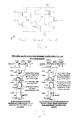
- FIG. 1 schematically illustrates the occurrence of metastability within a buffer formed of two standard flip-flop circuits
- FIG. 2 schematically illustrates the occurrence of metastability within a synchroniser circuit comprising two dynamic buffers
- FIG. 3 schematically illustrates the use of pulse amplification circuitry to reduce the susceptibility to metastability of a synchroniser circuit comprising two dynamic buffers;
- FIG. 4 schematically illustrates a chain of skewed inverters serving as pulse amplifying circuitry
- FIG. 5 is a diagram schematically illustrating how pulse amplification between stages reduces metastability when used with dynamic buffers, but does not have this effect when used with standard flip-flops;
- FIG. 6 schematically illustrates a dynamic buffer stage including a chain of skewed inverters
- FIG. 7 schematically illustrates two synchronisers working in a ping-pong manner to serve as a synchroniser between two clock domains
- FIG. 8 is a flow diagram schematically illustrating operation of the circuitry of FIG. 4 .
- FIG. 2 illustrates synchroniser circuitry 2 for synchronising an input signal XCK 1 from a first clock domain operating with a clock signal CK 1 so as to form an output signal Y 2 in a second clock domain operating with a clock signal CK 2 .
- the synchroniser circuitry 2 comprises two dynamic buffer circuits 4 , 6 .
- the first dynamic buffer circuit 4 is shown in an exploded view in FIG. 2 .
- the first buffer circuit serves to charge a first node 8 to a high signal value (VDD) during the low phase of the clock signal CK through a P-type transistor 10 .
- Feedback circuitry comprising a small P-type transistor 12 and an inverter 14 serve as keeper circuitry to hold the first node 8 at this high signal value (VDD) unless the keeper circuitry 12 , 14 is overcome by the action of N-type transistors 16 , 18 .
- N-type transistors 16 , 18 During the high phase of the clock signal CK, if the input signal X is also high, then both of the N-type transistors 16 , 18 are conductive and the first node 8 will be discharged to ground.
- the low phase of the clock signal CK corresponds to the reset period of the dynamic buffer 4 and the high phase of the clock signal CK corresponds to the evaluate period.
- Scenario 1 corresponding to the situation illustrated in FIG. 1 which gave rise to metastability in a synchroniser circuit comprising two standard flip-flop circuits.
- the input signal is transitioning at the start of the evaluate period, then output of the first stage Y 1 may not immediately resolve. However, as the evaluate period continues it is likely that the signal Y 1 will resolve away from a metastable state.
- the nature of the dynamic buffers is such that the second stage 6 will respond to such an intermediate voltage in a manner in which the output Y 2 of the second stage 6 is fully resolved and accordingly there is no metastability in the output of the synchroniser 2 as a whole.
- Scenario 2 in FIG. 1 illustrates a form of metastability that can arise in the synchroniser 2 of FIG. 2 .
- This metastability arises as a consequence of a pulse occurring in the output Y 1 of the first stage 4 resulting in partial evaluation of the dynamic node (first node 8 ) and pull up by the keeper circuitry 12 , 14 .
- the input signal XCK 1 is such that a short duration pulse occurs in the output Y 1 of the first stage 4 , then this short duration pulse can result in the second stage 6 becoming metastable as its state node may be only partially discharged and its output signal Y 2 may not have fully resolved by the output observation time expected form the synchroniser 2 .
- metastability arising for the reason illustrated in FIG. 1 does not occur with the dynamic buffer circuit of FIG. 2
- there is a different potential type of metastability as a consequence of a pulse occurring in an intermediate signal between the synchroniser stages, as illustrated in Scenario 2 of FIG. 2 .
- FIG. 3 schematically illustrates synchroniser circuitry 2 formed of a first stage 4 and a second stage 6 with pulse amplifying circuitry 8 disposed therebetween.
- This pulse amplifying circuitry 8 is formed of a serially connected chain of skewed inverter circuits 20 , 22 , which alternate between being N-skewed and being P-skewed.
- the action of such skewed inverters 20 , 22 is to amplify a pulse of greater than a predetermined magnitude passing along the chain of skewed inverters 20 , 22 as is illustrated in FIG. 3 .
- a pulse of less than a predetermined magnitude will be made smaller by the action of the skewed inverters 20 , 22 .
- the second stage 6 is less likely to enter a metastable state as it receives a pulse of a greater magnitude increasing the probability that its state node will be fully discharged or a pulse that is too small to partially discharge its state node in a problematic manner.
- FIG. 3 illustrates an input signal XCK 1 received by the first stage 4 together with a clock signal CK 2 of the target domain.
- Output from the first stage 4 corresponds to a first stage state signal Y 1 .
- This first stage state signal Y 1 is passed to the pulse amplifying circuitry 8 where it is subject to pulse amplification as illustrated in FIG. 3 .
- the pulse amplified signal Y 1 _ b is supplied as an input to the second stage 6 .
- the output from the second stage 6 is signal Y 2 .
- the second stage 6 includes output generating circuitry, which generates this output signal Y 2 in dependence upon a second stage state signal within the second stage 6 . In some embodiments it is possible that the output signal Y 2 could be directly formed by the second stage state signal, in which case the output generating circuitry may simply be a conductor passing the second stage state signal out from the second stage 6 .
- the graphs illustrated in FIG. 3 illustrate how the calculated metastability window in the case of a double flip-flop standard synchroniser compares with that of a dynamic synchroniser with the pulse amplification circuitry as illustrated in FIG. 3 varies as the number of skewed inverters provided between the stages increases.
- the addition of the skewed inverters reduces the available resolution time in the flip-flop synchronisers, thereby increasing the metastability window and worsening the mean time before failure of the synchroniser.
- the addition of the skewed inverters improves pulse amplification and accordingly reduces the metastability window and improves the mean time before failure of the synchroniser.
- FIG. 3 further includes a graph illustrating how the gain of a skewed inverter stage varies with the degree of skew present within the inverter stage. This graph illustrates how a skew increases the normalised gain first increases and then starts to decrease. While skew alignment improves gain, the present technique does not require such skew alignment to be optimised.
- FIG. 4 schematically illustrates pulse amplification circuitry 8 in the form of a serially connected chain of skewed inverters.
- the inverters are skewed by virtue of one of the transistors within each inverter stack being stronger than the other transistor within that same stack.
- the P-type transistor is stronger than the N-type transistor. The converse is true in an N-skewed inverter.
- FIG. 5 schematically illustrates how pulse amplification between synchroniser stages helps reduce the likelihood of metastability when the synchroniser stages are dynamic synchroniser stages (right hand side of FIG. 5 ), whereas in the case of a synchroniser formed of conventional flip-flops, and including pulse amplification circuitry, the effect of pulse amplification can be to increase the susceptibility to metastability (left hand side of FIG. 5 ).
- the effect of pulse amplification is to amplify a signal Y 1 a to form a signal Y 1 b with a larger magnitude when the signal Y 1 a has greater than a predetermined magnitude (the amplifying circuitry also acts to suppress small pulses that have less than a predetermined magnitude).
- the larger magnitude of the signal Y 1 b has the effect of reducing the likelihood that the output from the second stage Y 2 will be metastable, as even if the pulse Y 1 b resolves back to a value of “0”, then a magnitude of the duration of this pulse (the “impulse”) is sufficiently large that the second stage dynamic synchroniser will have fully resolved and evaluated the output signal Y 2 to a non-metastable value.
- conventional flip-flop circuits can degrade in performance as an amplified pulse Q 1 b can result in a falling edge of that pulse occurring at the time at which the second flip-flop stage is sampling its input, and this can result in the output of the second stage Q 2 becoming metastable.
- FIG. 6 schematically illustrates synchroniser circuitry 24 comprising more than two dynamic stages (e.g. in this example three dynamic stages).
- Each of the dynamic stages includes stage reset circuitry in the form of a P-type transistor 26 .
- Keeper circuitry is provided by the inverter 28 and a small P-type transistor 30 .
- Output capture circuitry is provided by N-type transistors 32 , 34 which selectively discharge a stage node 36 during an evaluation period when a clock signal CK 2 is high. When the clock signal CK 2 is low, this is the reset period during which the reset circuitry in the form of the P-type transistor 26 serves to charge the stage node 36 high to the VDD voltage.
- Each dynamic synchroniser stage includes a serially connected chain of skewed inverters (N, P, N, P, N, P) which serves as pulse amplifying circuitry.
- the final inverter may also be considered to serve as output generating circuitry to generate an output signal, at least in the case of the final stage within the synchroniser circuitry 24 .
- a cut-off transistor M 1 serves to improve the characteristics of the signal on the stage node 36 when switching between its high (reset) state and its low (set) state.
- FIG. 7 schematically illustrates a buffer unit 38 in the form of two dynamic synchronisers (each comprising multiple dynamic stages) connected back-to-back in a ping-pong manner.
- dynamic synchroniser DS 1 When dynamic synchroniser DS 1 is in its reset period, dynamic synchroniser DS 2 is in its evaluate period. The converse is true when the controlling clock signal CK 2 changes its phase. In this manner, the dynamic synchroniser always serves to pass a data_in signal it receives through the buffer unit 38 to an OR gate 40 which generates an output signal. Accordingly, the latency associated with pre-charging the individual dynamic synchronisers may be hidden.
- FIG. 8 is a flow diagram schematically illustrating the operation of dynamic synchronising circuitry illustrated in FIG. 3 .
- an input signal is received at the first circuit stage and serves to generate a first stage state signal at a first stage node.
- the pulse amplifying circuitry 8 serves to pulse amplify the first stage state signal to generate a pulse amplified signal.
- the first stage state signal may remain at its reset value, in which case the pulse amplification circuitry 8 has no effect.
- the first stage state signal may discharge to its set value.
- the pulse amplification circuitry 8 may have the effect of increasing in the rate of change of the signal supplied to the second stage up to the point where it reaches the set value, and then remains at the set value.
- the first stage state signal shows a pulse behaviour in which it changes and moves away from the reset value towards the set value, and then returns to the reset value.
- the pulse amplification circuitry serves to increase the magnitude of the pulse corresponding to these changes and with a predetermined range of magnitudes, as is illustrated in FIG. 3 .
- the pulse amplified signal which is so generated has an increased probability of causing a full transition in the second stage thereby reducing the probability of metastability arising in the output of the second stage. Pulses that are too small are suppressed by the pulse amplification.
- the pulse amplified signal is received by the second circuit stage 6 .
- the second circuit stage either changes or maintains the second stage state signal in dependence upon the pulse amplified signal that is received.
- the pulse amplified signal may not necessarily contain a pulse, but any pulse therein will be amplified in magnitude.
- an output signal is generated in dependence upon the second stage state signal. In some embodiments the second stage state signal could directly serve as the output signal.
Abstract
Synchronisation circuitry 2 comprises a first dynamic circuit stage 4 generating a first stage state signal which is pulse amplified by pulse amplifying circuitry 8 to generate a pulse amplified signal. The pulse amplified signal is supplied to a second dynamic circuit stage 6 where it is used to control generation of a second stage state signal. The pulse amplifying circuitry 8 comprises a chain of serially connected skewed inverters 20, 22. The action of the pulse amplifying circuitry 8 is to reduce the probability of metastability in the output of the second dynamic stage 6.
Description
1. Field of the Invention
This invention relates to the field of circuitry for processing digital signals. More particularly, this invention relates to dynamic circuitry having state signal which is reset to a predetermined value and then selectively changed from that predetermined value in dependence upon an input signal value.
2. Description of the Prior Art
A known problem within circuitry for processing digital signals is metastability. Metastability can arise when a signal value is sampled at a time close to when that signal value undergoes a transition. For example, a buffer circuit as illustrated in FIG. 1 of the accompanying drawings may serve as a synchroniser between clock domains and uses conventional flip-flops rather than dynamic circuits (buffers). The circuitry of FIG. 1 is configured to sample an input signal DCK1 from clock domain CK1 upon the rising edge of a different clock signal CK2. As illustrated in FIG. 1 , if the input signal DCK1 undergoes a transition close to the rising edge of the clock signal CK2, then the output of the first flip-flop DFF1 can become metastable and adopt an intermediate signal value rather than clearly adopting either the high voltage state or the low voltage state. The metastability of the signal Q1 output from the first flip-flop DFF1, may then go on to produce metastability in the output of the second flip-flop DFF2 as illustrated. Such metastability problems become more of a concern when the design of a circuit is such that the proper value for the input signal DCK1 will not settle until shortly before the time at which it will be sampled. Indeed, in order to increase the performance of some circuits, it is known to increase the clock frequency to reach a limiting condition in which input signals to be sampled settle to their true values just before the time at which they are sampled. While this approach may increase the performance of the circuitry, it also increases the probability of errors occurring due to metastability as illustrated in FIG. 1 .
Viewed from one aspect the present invention provides circuitry for receiving an input signal having an input signal value and for generating an output signal having an output signal value dependent upon said input signal value, said buffer circuit comprising:
a first circuit stage configured to receive said input signal and to generate a first stage state signal in dependence upon said input signal;
pulse amplifying circuitry configured to receive and to pulse amplify said first stage state signal to generate a pulse amplified signal having a pulse amplified signal value such that a pulse in said first stage state signal, during which said first stage state signal changes from a first state signal value toward a second state signal value and then returns to said first state signal value, is amplified;
a second circuit stage comprising:
-
- second stage reset circuitry configured to reset a second stage state signal to a second stage reset signal value during a second stage reset period;
- output capture circuitry configured to receive said pulse amplified signal during a second stage evaluation period and:
- (i) if said pulse amplified signal value has a first value, then to leave said second stage state signal at said second stage reset signal value; and
- (ii) if said pulse amplified signal value has a second value, then to change said second stage state signal from said second stage reset signal value to a second stage set signal value; and
output generating circuitry configured to generate said output signal in dependence upon said second stage state signal.
The present technique provides circuitry including at least a second circuit stage configured as a dynamic circuit. Such a dynamic stage is reset to provide a reset signal value during a reset period and then during an evaluation period that signal value is selectively changed to a set signal value if a received input to the stage has a predetermined value. Once the reset signal value has changed to the set signal value, then it does not change back during the evaluation period, even if the input signal value changes. While this approach has less vulnerability to metastability arising from the precise timing of an input signal relative to a sampling clock edge as illustrated in FIG. 1 , and instead evaluates the input signal over a more extended evaluation period, the dynamic stage has a vulnerability to metastability caused by pulses in the signal being detected. A pulse in the signal being detected may have a magnitude and a duration such that the signal value being controlled by the second stage does not fully change from the reset signal value to the set signal value. This produces metastability in the output of the second stage. In order to address this problem, the present technique provides pulse amplifying circuitry configured to receive the signal to be evaluated by the second stage and to amplify pulses in that signal prior to passing pulse amplified signal values so generated onto the second circuit stage where the pulse amplified signal value serves to selectively switch the second circuit stage from the reset state to the set state. The action of the pulse amplifying circuitry is that pulses having greater than a predetermined magnitude are increased in magnitude and pulses having less than a predetermined magnitude are diminished in magnitude. This reduces the range (likelihood) of pulses that can cause problematic metastability pulses that without the action of the amplifying circuitry cause metastability are now mostly either increased in magnitude so that they fully switch the second stage or are reduced in magnitude such that the second stage is clearly not switched. The greater the magnitude of the amplification provided by the pulse amplifying circuitry, the less the statistical likelihood of metastability arising as a consequence of a certain range of pulses in the signal being sampled by the second circuit stage.
It will be appreciated that the second circuitry stage described above is a dynamic circuit which is reset to have a reset state and is then changed to the set state in dependence upon an input signal value. The first circuit stage, which receives the input signal into the circuitry as a whole, could have a variety of different forms. In some forms of the present technique, this first circuit stage is also a dynamic circuit with its own reset and set states. In such embodiments, the pulse amplifying circuitry is disposed between two dynamic buffer stages.
In embodiments in which the circuitry in accordance with the present technique is to be used as a buffer between two domains (e.g. clock domains or voltage domains), then this may be conveniently achieved by providing that the first stage reset period and the second stage reset period at least partially overlap and that the first stage evaluation period and the second stage evaluation period at least partially overlap. In this way, an input signal can be passed through to the output of the circuitry with a low delay.
The coordination between the action of the first stage and the second stage may be achieved when the first stage reset circuitry and the second stage reset circuitry are configured to be driven by a shared clock signal with a first phase of that shared clock signal corresponding to the first stage reset period and the second stage reset period and a second phase of that shared clock signal corresponding to the first stage evaluation period and the second stage evaluation period. The shared clock signal coordinates the action of the first stage circuitry and the second stage circuitry.
The dynamic circuitry forming the second stage circuitry may be provided using a second stage node which is precharged to the reset signal value and then selectively discharged to a set signal value in dependence upon the pulse amplified signal value. Keeper circuitry may be associated with the second stage node to hold the second stage node at the reset signal value unless the keeper circuitry is overcome by the output capture circuitry and the second stage node is discharged.
In embodiments in which the first stage circuitry is also dynamic, then a similar arrangement of a first stage node and first stage keeper circuitry may be employed therein.
The present technique may be used with only first stage circuitry and second stage circuitry having pulse amplifying circuitry disposed between. However, in other embodiments, it is possible that one or more further circuit stages may be provided and serially connected between the second circuit stage and the output generating circuitry. Further pulse amplifying circuitry may be disposed between some or all of the adjacent circuit stages in the arrangement where one or more further circuit stages are provided.
It will be appreciated that the pulse amplifying circuitry can have a variety of different forms. In one example form, the pulse amplifying circuitry may be of a skewed inverter circuit that is configured to drive the pulse amplifying signal to change with a greater drive strength in a first direction than in an opposite direction. Other forms of pulse amplifying circuitry are also possible, and may be mixed with, or used instead of, skewed inverters.
In one embodiment the pulse amplifying circuitry may comprise a chain of skewed inverters with adjacent skewed inverters within the chain having drive strengths skewed in opposite directions.
While the present circuitry can have a variety of different possible uses, one particular use is as a synchroniser for synchronising an input signal from a first clock domain to a clock signal of a second clock domain. In this context, the circuitry of the present technique provides a reduced vulnerability to metastability when there is a change in clock domain. Such a form of the circuitry is a synchronising buffer circuit.
The problems associated with metastability are increased embodiments in which input generating circuitry is configured to dynamically tune the input signal such that a valid transition of the input signal value completes at a time corresponding to the beginning of the first stage evaluation period. Such embodiments may be using the “Razor” techniques described in WO-A-2004/084072. Such embodiments the present technique has a strong advantage of reducing the vulnerability of the metastability.
Circuitry in accordance with the present techniques may be employed in pairs to produce two synchronisers working in a ping-pong manner to provide synchronisation between clock domains such that when first circuitry in accordance with the present technique is in its evaluation period, second circuitry associated with the present technique is in its reset period and vice versa.
Viewed from another aspect the present invention provides circuitry for receiving an input signal having an input signal value and for generating an output signal having an output signal value dependent upon said input signal value, said buffer circuit comprising:
first circuit stage means for receiving said input signal and for generating a first stage state signal in dependence upon said input signal;
pulse amplifying circuitry for receiving and for pulse amplifying said first stage state signal to generate a pulse amplified signal having a pulse amplified signal value such that a pulse in said first stage state signal, during which said first stage state signal changes from a first state signal value toward a second state signal value and then returns to said first state signal value, is amplified;
a second circuit stage comprising:
second stage reset means for resetting a second stage state signal to a second stage reset signal value during a second stage reset period;
output capture means for receiving said pulse amplified signal during a second stage evaluation period and:
-
- (i) if said pulse amplified signal value has a first value, then leaving said second stage state signal at said second stage reset signal value; and
- (ii) if said pulse amplified signal value has a second value, then changing said second stage state signal from said second stage reset signal value to a second stage set signal value; and
output generating means for generating said output signal in dependence upon said second stage state signal.
Viewed from a further aspect the present invention provides a method of operating circuitry for receiving an input signal having an input signal value and for generating an output signal having an output signal value dependent upon said input signal value, said method comprising the steps of:
receiving at a first circuit stage said input signal and generating a first stage state signal in dependence upon said input signal;
pulse amplifying said first stage state signal to generate a pulse amplified signal having a pulse amplified signal value such that a pulse in said first stage state signal, during which said first stage state signal changes from a first state signal value toward a second state signal value and then returns to said first state signal value, is amplified;
resetting a second stage state signal to a second stage reset signal value during a second stage reset period;
receiving said pulse amplified signal during a second stage evaluation period and:
-
- (i) if said pulse amplified signal value has a first value, then leaving said second stage state signal at said second stage reset signal value; and
- (ii) if said pulse amplified signal value has a second value, then changing said second stage state signal from said second stage reset signal value to a second stage set signal value; and
generating said output signal in dependence upon said second stage state signal.
The above, and other objects, features and advantages of this invention will be apparent from the following detailed description of illustrative embodiments which is to be read in connection with the accompanying drawings.
Illustrated in FIG. 2 is Scenario 1 corresponding to the situation illustrated in FIG. 1 which gave rise to metastability in a synchroniser circuit comprising two standard flip-flop circuits. In this case, if the input signal is transitioning at the start of the evaluate period, then output of the first stage Y1 may not immediately resolve. However, as the evaluate period continues it is likely that the signal Y1 will resolve away from a metastable state. However, even during the period when the output of the first stage 4 is still unresolved, and the signal Y1 has an intermediate voltage value, the nature of the dynamic buffers is such that the second stage 6 will respond to such an intermediate voltage in a manner in which the output Y2 of the second stage 6 is fully resolved and accordingly there is no metastability in the output of the synchroniser 2 as a whole.
The graphs illustrated in FIG. 3 illustrate how the calculated metastability window in the case of a double flip-flop standard synchroniser compares with that of a dynamic synchroniser with the pulse amplification circuitry as illustrated in FIG. 3 varies as the number of skewed inverters provided between the stages increases. In the case of standard flip-flop circuitry, the addition of the skewed inverters reduces the available resolution time in the flip-flop synchronisers, thereby increasing the metastability window and worsening the mean time before failure of the synchroniser. Conversely, in the case of the dynamic stage synchronisers illustrated in FIG. 3 , the addition of the skewed inverters improves pulse amplification and accordingly reduces the metastability window and improves the mean time before failure of the synchroniser.
In contrast to the behaviour of the dynamic synchroniser stages in response to pulse amplification, conventional flip-flop circuits can degrade in performance as an amplified pulse Q1 b can result in a falling edge of that pulse occurring at the time at which the second flip-flop stage is sampling its input, and this can result in the output of the second stage Q2 becoming metastable.
At step 46 the pulse amplified signal is received by the second circuit stage 6. At step 48 the second circuit stage either changes or maintains the second stage state signal in dependence upon the pulse amplified signal that is received. The pulse amplified signal may not necessarily contain a pulse, but any pulse therein will be amplified in magnitude. At step 50, an output signal is generated in dependence upon the second stage state signal. In some embodiments the second stage state signal could directly serve as the output signal.
Although illustrative embodiments of the invention have been described in detail herein with reference to the accompanying drawings, it is to be understood that the invention is not limited to those precise embodiments, and that various changes and modifications can be effected therein by one skilled in the art without departing from the scope and spirit of the invention as defined by the appended claims.
Claims (19)
1. Circuitry for receiving an input signal having an input signal value and for generating an output signal having an output signal value dependent upon said input signal value, said buffer circuit comprising:
a first circuit stage configured to receive said input signal and to generate a first stage state signal in dependence upon said input signal;
pulse amplifying circuitry configured to receive and to pulse amplify said first stage state signal to generate a pulse amplified signal having a pulse amplified signal value such that a pulse in said first stage state signal, during which said first stage state signal changes from a first state signal value toward a second state signal value and then returns to said first state signal value, is amplified;
a second circuit stage comprising:
second stage reset circuitry configured to reset a second stage state signal to a second stage reset signal value during a second stage reset period;
output capture circuitry configured to receive said pulse amplified signal during a second stage evaluation period and:
(i) if said pulse amplified signal value has a first value, then to leave said second stage state signal at said second stage reset signal value; and
(ii) if said pulse amplified signal value has a second value, then to change said second stage state signal from said second stage reset signal value to a second stage set signal value; and
output generating circuitry configured to generate said output signal in dependence upon said second stage state signal.
2. Circuitry as claimed in claim 1 , wherein said first circuit stage comprises:
first stage reset circuitry configured to reset a first stage state signal to a first stage reset signal value during a first stage reset period; and
input detecting circuitry configured to receive said input signal during a first stage evaluation period and:
(i) if said input signal value has a third value, then to change said first stage state signal from said first stage reset signal value to a first stage set signal value; and
(ii) if said input signal value has a fourth value, then to leave said first stage state signal at said first stage reset signal value.
3. Circuitry as claimed in claim 2 , wherein said first stage reset period and said second stage reset period at least partially overlap and said first stage evaluation period and said second stage evaluation period at least partially overlap.
4. Circuitry as claimed in claim 3 , wherein said first stage reset circuitry and said second stage reset circuitry are configured to be driven by a shared clock signal, a first phase of said shared clock signal corresponding to said first stage reset period and said second stage reset period and a second phase of said shared clock signal corresponding to said first stage evaluation period and said second stage evaluation period.
5. Circuitry as claimed in claim 1 , wherein second stage reset circuitry is configured to precharge a second stage node to said second stage reset signal value during said second stage reset period and said output capture circuitry is configured to discharge said second stage node toward said second stage set signal value if said pulse amplified signal value has said first value during said second stage evaluation period.
6. Circuitry as claimed in claim 5 , comprising second stage keeper circuitry configured to maintain said second stage node at said second stage reset signal value during said second stage evaluation period unless said output capture circuitry overcomes said second stage keeper circuitry and discharges said second stage node.
7. Circuitry as claimed in claim 2 , wherein first stage reset circuitry is configured to precharge a first stage node to said first stage reset signal value during said first stage reset period and said input detecting circuitry is configured to discharge said first stage node toward said first stage set signal value if said input signal value has said third value during said first stage evaluation period.
8. Circuitry as claimed in claim 7 , comprising first stage keeper circuitry configured to maintain said first stage node at said first stage reset signal value during said first stage evaluation period unless said input detecting circuitry overcomes said first stage keeper circuitry and discharges said first stage node.
9. Circuitry as claimed in claim 1 , comprising one or more further circuit stages serially connected between said second circuit stage and said output generating circuitry and pulse amplifying circuitry disposed between some or all adjacent circuit stages and configured to pulse amplify any pulse in a signal passed between said adjacent circuit stages.
10. Circuitry as claimed in claim 1 , wherein said pulse amplifying circuitry comprises at least one skewed invertor circuit configured to drive said pulse amplified signal value to change with a greater drive strength in a first direction, in response to said first stage state signal changing from said first stage reset signal value toward said first stage set signal value, than in a second direction opposite to said first direction.
11. Circuitry as claimed in claim 10 , wherein said pulse amplifying circuitry comprises a chain of skewed invertor circuits.
12. Circuitry as claimed in claim 11 , wherein adjacent skewed invertor circuits within said chain have drive strengths skewed in opposite directions.
13. Circuitry as claimed in claim 1 , wherein said second circuit stage is vulnerable to metastability if said first stage state signal value includes a pulse during said first stage evaluation period and said pulse amplification of said first stage state signal by said pulse amplifying circuitry reduces a probability of said metastability arising.
14. Circuitry as claimed in claim 1 , wherein said circuitry is synchroniser circuitry configured to synchronise said input signal from a first clock domain with a clock signal of a second domain to generate said output signal.
15. Circuitry as claimed in claim 1 , wherein said circuitry is configured as buffer circuitry.
16. Processing circuitry comprising:
circuitry as claimed in claim 2 , and
input generating circuitry configured to dynamically tune said input signal such that a valid transition in said input signal value completes at a time corresponding to a beginning of said first stage evaluation period.
17. A buffer unit comprising:
first circuitry as claimed in claim 1 , and
second circuitry as claimed in claim 1 , wherein
said first circuitry and said second circuitry share said input signal and share said output signal;
said first stage reset period of said first circuitry corresponds to said first stage evaluation period of said second circuitry;
said first stage evaluation period of said first circuitry corresponds to said first stage reset period of said second circuitry;
said second stage reset period of said first circuitry corresponds to said second stage evaluation period of said second circuitry; and
said second stage evaluation period of said first circuitry corresponds to said second stage reset period of said second circuitry.
18. Circuitry for receiving an input signal having an input signal value and for generating an output signal having an output signal value dependent upon said input signal value, said buffer circuit comprising:
first circuit stage means for receiving said input signal and for generating a first stage state signal in dependence upon said input signal;
pulse amplifying circuitry for receiving and for pulse amplifying said first stage state signal to generate a pulse amplified signal having a pulse amplified signal value such that a pulse in said first stage state signal, during which said first stage state signal changes from a first state signal value toward a second state signal value and then returns to said first state signal value, is amplified;
a second circuit stage comprising:
second stage reset means for resetting a second stage state signal to a second stage reset signal value during a second stage reset period;
output capture means for receiving said pulse amplified signal during a second stage evaluation period and:
(i) if said pulse amplified signal value has a first value, then leaving said second stage state signal at said second stage reset signal value; and
(ii) if said pulse amplified signal value has a second value, then changing said second stage state signal from said second stage reset signal value to a second stage set signal value; and
output generating means for generating said output signal in dependence upon said second stage state signal.
19. A method of operating circuitry for receiving an input signal having an input signal value and for generating an output signal having an output signal value dependent upon said input signal value, said method comprising the steps of:
receiving at a first circuit stage said input signal and generating a first stage state signal in dependence upon said input signal;
pulse amplifying said first stage state signal to generate a pulse amplified signal having a pulse amplified signal value such that a pulse in said first stage state signal, during which said first stage state signal changes from a first state signal value toward a second state signal value and then returns to said first state signal value, is amplified;
resetting a second stage state signal to a second stage reset signal value during a second stage reset period;
receiving said pulse amplified signal during a second stage evaluation period and:
(i) if said pulse amplified signal value has a first value, then leaving said second stage state signal at said second stage reset signal value; and
(ii) if said pulse amplified signal value has a second value, then changing said second stage state signal from said second stage reset signal value to a second stage set signal value; and
generating said output signal in dependence upon said second stage state signal.
Priority Applications (1)
| Application Number | Priority Date | Filing Date | Title |
|---|---|---|---|
| US13/940,864 US9490779B2 (en) | 2013-07-12 | 2013-07-12 | Dynamic circuitry using pulse amplification to reduce metastability |
Applications Claiming Priority (1)
| Application Number | Priority Date | Filing Date | Title |
|---|---|---|---|
| US13/940,864 US9490779B2 (en) | 2013-07-12 | 2013-07-12 | Dynamic circuitry using pulse amplification to reduce metastability |
Publications (2)
| Publication Number | Publication Date |
|---|---|
| US20150015305A1 US20150015305A1 (en) | 2015-01-15 |
| US9490779B2 true US9490779B2 (en) | 2016-11-08 |
Family
ID=52276625
Family Applications (1)
| Application Number | Title | Priority Date | Filing Date |
|---|---|---|---|
| US13/940,864 Active 2035-09-03 US9490779B2 (en) | 2013-07-12 | 2013-07-12 | Dynamic circuitry using pulse amplification to reduce metastability |
Country Status (1)
| Country | Link |
|---|---|
| US (1) | US9490779B2 (en) |
Citations (5)
| Publication number | Priority date | Publication date | Assignee | Title |
|---|---|---|---|---|
| US4933571A (en) * | 1987-09-17 | 1990-06-12 | Siemens Aktiengesellschaft | Synchronizing flip-flop circuit configuration |
| US5418407A (en) * | 1992-03-19 | 1995-05-23 | Vlsi Technology, Inc. | Asynchronous to synchronous particularly CMOS synchronizers |
| US5654988A (en) * | 1995-09-29 | 1997-08-05 | Intel Corporation | Apparatus for generating a pulse clock signal for a multiple-stage synchronizer |
| US5764710A (en) * | 1995-12-15 | 1998-06-09 | Pericom Semiconductor Corp. | Meta-stable-resistant front-end to a synchronizer with asynchronous clear and asynchronous second-stage clock selector |
| US7977975B1 (en) * | 2009-09-18 | 2011-07-12 | Altera Corporation | Apparatus for using metastability-hardened storage circuits in logic devices and associated methods |
-
2013
- 2013-07-12 US US13/940,864 patent/US9490779B2/en active Active
Patent Citations (5)
| Publication number | Priority date | Publication date | Assignee | Title |
|---|---|---|---|---|
| US4933571A (en) * | 1987-09-17 | 1990-06-12 | Siemens Aktiengesellschaft | Synchronizing flip-flop circuit configuration |
| US5418407A (en) * | 1992-03-19 | 1995-05-23 | Vlsi Technology, Inc. | Asynchronous to synchronous particularly CMOS synchronizers |
| US5654988A (en) * | 1995-09-29 | 1997-08-05 | Intel Corporation | Apparatus for generating a pulse clock signal for a multiple-stage synchronizer |
| US5764710A (en) * | 1995-12-15 | 1998-06-09 | Pericom Semiconductor Corp. | Meta-stable-resistant front-end to a synchronizer with asynchronous clear and asynchronous second-stage clock selector |
| US7977975B1 (en) * | 2009-09-18 | 2011-07-12 | Altera Corporation | Apparatus for using metastability-hardened storage circuits in logic devices and associated methods |
Non-Patent Citations (7)
Also Published As
| Publication number | Publication date |
|---|---|
| US20150015305A1 (en) | 2015-01-15 |
Similar Documents
| Publication | Publication Date | Title |
|---|---|---|
| US10340917B2 (en) | Receiver circuitry and method for converting an input signal from a source voltage domain into an output signal for a destination voltage domain | |
| CN101740097A (en) | Data transmitting system | |
| JP6239790B2 (en) | Broadband duty cycle correction circuit | |
| US11808798B2 (en) | Jitter noise detector | |
| US8330517B1 (en) | Bistable circuit with metastability resistance | |
| WO2016108989A1 (en) | Cross-coupled level shifter with transition tracking circuits | |
| US9590602B2 (en) | System and method for a pulse generator | |
| US7932750B2 (en) | Dynamic domino circuit and integrated circuit including the same | |
| JPS61267414A (en) | Symmetrical output complementary buffer circuit | |
| US7714632B2 (en) | Clock control circuit and semiconductor integrated circuit using the same | |
| US7528630B2 (en) | High speed flip-flop | |
| US11073862B2 (en) | Synchronization circuit and cascaded synchronization circuit for converting asynchronous signal into synchronous signal | |
| US9490779B2 (en) | Dynamic circuitry using pulse amplification to reduce metastability | |
| US9362899B2 (en) | Clock regenerator | |
| US20100176857A1 (en) | Apparatus for outputting complementary signals using bootstrapping technology | |
| US8432195B2 (en) | Latch circuits with synchronous data loading and self-timed asynchronous data capture | |
| US11115034B2 (en) | Signal detection circuit and signal detection method | |
| US9214944B2 (en) | Digital counter | |
| US8692581B2 (en) | Constant switching current flip-flop | |
| US20210225252A1 (en) | Shift register unit, gate driving circuit and driving method | |
| US9479147B2 (en) | Synchroniser flip-flop | |
| US20120105156A1 (en) | Receiver circuit of semiconductor apparatus and method for receiving signal | |
| US9774326B2 (en) | Circuit and method for generating clock-signals | |
| KR100613458B1 (en) | Flip flop | |
| US20180226968A1 (en) | Contention-Free Dynamic Logic |
Legal Events
| Date | Code | Title | Description |
|---|---|---|---|
| AS | Assignment |
Owner name: THE REGENTS OF THE UNIVERSITY OF MICHIGAN, MICHIGA Free format text: ASSIGNMENT OF ASSIGNORS INTEREST;ASSIGNORS:SYLVESTER, DENNIS;BLAAUW, DAVID T.;FICK, DAVID ALAN;AND OTHERS;SIGNING DATES FROM 20130801 TO 20130809;REEL/FRAME:031338/0078 |
|
| STCF | Information on status: patent grant |
Free format text: PATENTED CASE |
|
| MAFP | Maintenance fee payment |
Free format text: PAYMENT OF MAINTENANCE FEE, 4TH YEAR, LARGE ENTITY (ORIGINAL EVENT CODE: M1551); ENTITY STATUS OF PATENT OWNER: LARGE ENTITY Year of fee payment: 4 |