US9479142B1 - Phase error compensation circuit - Google Patents
Phase error compensation circuit Download PDFInfo
- Publication number
- US9479142B1 US9479142B1 US14/806,478 US201514806478A US9479142B1 US 9479142 B1 US9479142 B1 US 9479142B1 US 201514806478 A US201514806478 A US 201514806478A US 9479142 B1 US9479142 B1 US 9479142B1
- Authority
- US
- United States
- Prior art keywords
- circuit
- differential
- transconductance
- coupled
- multiplier
- Prior art date
- Legal status (The legal status is an assumption and is not a legal conclusion. Google has not performed a legal analysis and makes no representation as to the accuracy of the status listed.)
- Active
Links
- 238000000034 method Methods 0.000 claims abstract description 13
- 230000010363 phase shift Effects 0.000 description 17
- 230000008901 benefit Effects 0.000 description 7
- 238000010586 diagram Methods 0.000 description 4
- 230000014509 gene expression Effects 0.000 description 4
- 230000008859 change Effects 0.000 description 3
- 239000003990 capacitor Substances 0.000 description 2
- 238000006243 chemical reaction Methods 0.000 description 2
- 230000001934 delay Effects 0.000 description 2
- 230000003071 parasitic effect Effects 0.000 description 2
- 230000008569 process Effects 0.000 description 2
- 230000004044 response Effects 0.000 description 2
- 230000009471 action Effects 0.000 description 1
- 230000005540 biological transmission Effects 0.000 description 1
- 238000004891 communication Methods 0.000 description 1
- 230000000295 complement effect Effects 0.000 description 1
- 238000005516 engineering process Methods 0.000 description 1
- 238000005259 measurement Methods 0.000 description 1
Images


Classifications
-
- H—ELECTRICITY
- H03—ELECTRONIC CIRCUITRY
- H03L—AUTOMATIC CONTROL, STARTING, SYNCHRONISATION OR STABILISATION OF GENERATORS OF ELECTRONIC OSCILLATIONS OR PULSES
- H03L7/00—Automatic control of frequency or phase; Synchronisation
- H03L7/06—Automatic control of frequency or phase; Synchronisation using a reference signal applied to a frequency- or phase-locked loop
- H03L7/08—Details of the phase-locked loop
- H03L7/099—Details of the phase-locked loop concerning mainly the controlled oscillator of the loop
-
- H—ELECTRICITY
- H03—ELECTRONIC CIRCUITRY
- H03B—GENERATION OF OSCILLATIONS, DIRECTLY OR BY FREQUENCY-CHANGING, BY CIRCUITS EMPLOYING ACTIVE ELEMENTS WHICH OPERATE IN A NON-SWITCHING MANNER; GENERATION OF NOISE BY SUCH CIRCUITS
- H03B27/00—Generation of oscillations providing a plurality of outputs of the same frequency but differing in phase, other than merely two anti-phase outputs
-
- H—ELECTRICITY
- H03—ELECTRONIC CIRCUITRY
- H03H—IMPEDANCE NETWORKS, e.g. RESONANT CIRCUITS; RESONATORS
- H03H11/00—Networks using active elements
- H03H11/02—Multiple-port networks
- H03H11/16—Networks for phase shifting
- H03H11/18—Two-port phase shifters providing a predetermined phase shift, e.g. "all-pass" filters
-
- H—ELECTRICITY
- H03—ELECTRONIC CIRCUITRY
- H03D—DEMODULATION OR TRANSFERENCE OF MODULATION FROM ONE CARRIER TO ANOTHER
- H03D3/00—Demodulation of angle-, frequency- or phase- modulated oscillations
- H03D3/007—Demodulation of angle-, frequency- or phase- modulated oscillations by converting the oscillations into two quadrature related signals
- H03D3/009—Compensating quadrature phase or amplitude imbalances
-
- H—ELECTRICITY
- H03—ELECTRONIC CIRCUITRY
- H03D—DEMODULATION OR TRANSFERENCE OF MODULATION FROM ONE CARRIER TO ANOTHER
- H03D7/00—Transference of modulation from one carrier to another, e.g. frequency-changing
- H03D7/14—Balanced arrangements
- H03D7/1425—Balanced arrangements with transistors
- H03D7/1441—Balanced arrangements with transistors using field-effect transistors
-
- H—ELECTRICITY
- H03—ELECTRONIC CIRCUITRY
- H03D—DEMODULATION OR TRANSFERENCE OF MODULATION FROM ONE CARRIER TO ANOTHER
- H03D7/00—Transference of modulation from one carrier to another, e.g. frequency-changing
- H03D7/14—Balanced arrangements
- H03D7/1425—Balanced arrangements with transistors
- H03D7/1458—Double balanced arrangements, i.e. where both input signals are differential
-
- H—ELECTRICITY
- H03—ELECTRONIC CIRCUITRY
- H03H—IMPEDANCE NETWORKS, e.g. RESONANT CIRCUITS; RESONATORS
- H03H11/00—Networks using active elements
- H03H11/02—Multiple-port networks
- H03H11/16—Networks for phase shifting
- H03H11/22—Networks for phase shifting providing two or more phase shifted output signals, e.g. n-phase output
-
- H—ELECTRICITY
- H03—ELECTRONIC CIRCUITRY
- H03K—PULSE TECHNIQUE
- H03K5/00—Manipulating of pulses not covered by one of the other main groups of this subclass
- H03K5/01—Shaping pulses
- H03K5/02—Shaping pulses by amplifying
-
- H—ELECTRICITY
- H03—ELECTRONIC CIRCUITRY
- H03K—PULSE TECHNIQUE
- H03K5/00—Manipulating of pulses not covered by one of the other main groups of this subclass
- H03K5/22—Circuits having more than one input and one output for comparing pulses or pulse trains with each other according to input signal characteristics, e.g. slope, integral
- H03K5/26—Circuits having more than one input and one output for comparing pulses or pulse trains with each other according to input signal characteristics, e.g. slope, integral the characteristic being duration, interval, position, frequency, or sequence
-
- H—ELECTRICITY
- H03—ELECTRONIC CIRCUITRY
- H03D—DEMODULATION OR TRANSFERENCE OF MODULATION FROM ONE CARRIER TO ANOTHER
- H03D2200/00—Indexing scheme relating to details of demodulation or transference of modulation from one carrier to another covered by H03D
- H03D2200/0001—Circuit elements of demodulators
- H03D2200/0021—Frequency multipliers
-
- H—ELECTRICITY
- H03—ELECTRONIC CIRCUITRY
- H03D—DEMODULATION OR TRANSFERENCE OF MODULATION FROM ONE CARRIER TO ANOTHER
- H03D2200/00—Indexing scheme relating to details of demodulation or transference of modulation from one carrier to another covered by H03D
- H03D2200/0041—Functional aspects of demodulators
- H03D2200/0043—Bias and operating point
-
- H—ELECTRICITY
- H03—ELECTRONIC CIRCUITRY
- H03K—PULSE TECHNIQUE
- H03K5/00—Manipulating of pulses not covered by one of the other main groups of this subclass
- H03K2005/00286—Phase shifter, i.e. the delay between the output and input pulse is dependent on the frequency, and such that a phase difference is obtained independent of the frequency
Definitions
- This disclosure generally relates to correcting a phase error between in-phase and quadrature component signals.
- Wireless communication systems often use quadrature phase generators for a variety of modulation and demodulation purposes. For example, it is often desirable to generate a quadrature phase local oscillator (LO) signal for either the down-conversion of a received signal or the up-conversion of a signal to be transmitted.
- the quadrature LO signal includes a quadrature component (Q) that leads an in-phase component (I) in phase by exactly 90°.
- Q quadrature component
- I in-phase component
- quadrature LO generation circuits may have small errors from the perfect 90° phase quadrature.
- phase error can reduce the image rejection and, if not corrected, may ultimately degrade transceiver performance.
- phase shifter uses a current controlled phase shifter in each path, thereby creating two independent paths, one for the in-phase signal and one for the quadrature signal. Because they are independent, they are subject to mismatches in layout parasitics and process parameters.
- Each phase shifter uses a fixed capacitor and a fixed resistor architecture.
- the emitter resistance is changed allowing the “variable phase shift network 420 ” to “maintain phase quadrature over a 2:1 range of input frequencies.”
- the resistor and capacitor may need to be scaled with frequency.
- '715 a variable capacitive load is applied to the I and Q LO signals to shift the phase. Similar to '422, the '715 patent may also need to be scaled with frequency in order to provide a consistent operation over frequency.
- U.S. Pre-Grant Patent Publication 2012/0120992 U.S. Pat. Nos. 7,742,545, and 7,298,222 all use delay elements in each I and Q LO path to adjust the phase. These references are sensitive to frequency, because, for a given phase shift at a low frequency, a longer delay may need to be used than at a higher frequency, to obtain the same phase shift. It is with respect to these considerations and others that the present disclosure has been written.
- FIG. 1 is a block diagram of an example of a phase error compensation circuit.
- FIG. 2 is a block diagram of an example of a phase error compensation circuit that includes transconductance circuits and loads.
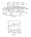
- FIG. 3 is a transistor level schematic of an example of a phase error compensation circuit.
- FIG. 4 is a graph illustrating an example of phase shift and control currents versus control value of an example phase error correction circuit.
- the various methods and circuits disclosed herein relate to correcting a phase error between in-phase and quadrature component signals, I and Q.
- the circuits discussed herein can correct for phase errors at high frequencies and may be used, for example, in local oscillator (LO) generation circuits.
- the phase error compensation circuit uses the I and Q LO signals to provide phase shifted signals.
- the circuits discussed herein do not require any capacitive loading or R-C and gate transmission delays to correct the relative phase error.
- FIG. 1 is a block diagram of a phase error compensation circuit, consistent with an exemplary embodiment.
- Circuit 100 includes multiplier circuits 101 and 103 .
- Complimentary local oscillator LOIP and LOIM signals may be received for the I signal and complementary local oscillator LOQP and LOQM may be received for the Q signal.
- V CI and V CQ may be DC voltages that represent an amount of phase correction for the I and Q signals, respectively.
- the LOIP/LOIM and LOQP/LOQM signals are pairs of differential signals.
- Eq. 3 provides that a small phase shift to LOI can be accomplished by subtracting a scaled amount of LOQ from LOI, where the phase shift ⁇ is given approximately by arcsine(A).
- a similar operation can be performed for a phase shift to LOQ by adding a scaled amount of LOI to LOQ.
- FIG. 2 is a block diagram of an example of a phase error compensation circuit that includes multiplier circuits 201 and 203 , transconductance circuits (amplifiers) g m , 205 and 208 , respectively, and resistances R LOAD 212 , 214 , 216 , and 218 , respectively.
- the exemplary embodiment of FIG. 2 illustrates a practical implementation, where the input signals are differential voltage pairs and are first applied to the transconductance amplifiers g m 205 and 208 , respectively, to change the input I and Q voltage signals into corresponding current signals.
- Circuit 200 is a phase error compensation circuit, consistent with an exemplary embodiment. It includes a first transconductance gm circuit (e.g., an amplifier) 205 having (i) a differential input configured to receive input signals LOIP IN and LOIM IN , and (ii) a differential output. There is a second transconductance gm circuit 208 having (i) a differential input configured to receive input signals LOQP IN and LOQM IN , and (ii) a differential output.
- the phase error compensation circuit 200 may include a transconductance amplifier 208 for the Q signal and a transconductance amplifier 205 for the I signal that change the I and Q signals from a varying voltage to a varying current that is proportional to the varying voltage.
- Circuit 200 includes a first multiplier circuit 201 and a second multiplier circuit 203 .
- circuit 200 illustrates a first multiplier circuit 201 having a differential input configured to receive a differential control signal V CI .
- the first multiplier circuit 201 includes a second differential input coupled to the differential output of the first transconductance circuit 205 and the differential output of the second multiplier circuit 203 .
- the first multiplier circuit 201 includes a differential output coupled to the differential output of the second transconductance circuit 208 .
- the second multiplier circuit 203 comprises a differential input configured to receive a differential control signal V CQ .
- the second multiplier circuit 203 includes a second differential input coupled to the differential output of the second transconductance circuit 208 and the differential output of the first multiplier circuit 201 .
- the second multiplier circuit 203 includes a differential output coupled to the differential output of the first transconductance circuit 205 .
- each transconductance amplifier 205 , 208 may pass through its corresponding multiplier circuit 201 , 203 , respectively.
- each multiplier circuit may be configured as a current attenuator.
- Circuit 200 includes a first differential load R LOAD 212 , 214 and a second differential load R LOAD 216 , 218 , all differential nodes sharing a common node that is set at a suitable voltage level (e.g., V CC , V DD , gnd., etc.).
- the first differential load comprises a first load 212 and a second load 214 , each receiving one component of the differential output LOIP OUT and LOIM OUT of the second multiplier circuit 203 .
- the second differential load comprises a first load 216 and a second load 218 , each receiving one component of the differential output LOQP OUT and LOQM OUT of the first multiplier circuit 201 .
- the outputs of the multipliers 201 , 203 are combined at least in part with the output signal from the transconductance circuits 205 , 208 .
- the differential loads i.e., R LOAD 212 with R LOAD 214 ; and R LOAD 216 with R LOAD 218 ) perform a summing operation, combining the output signal from the transconductance circuits with the output signals of the multiplier circuits.
- the summing operation is discussed in more detail later in the context of FIG. 3 .
- the phase error compensation circuit discussed herein generates a phase-corrected quadrature Q signal and a corresponding phase-corrected in-phase I signal.
- the phase error compensation circuit 200 may include an I multiplier circuit 201 that multiplies the I signal provided by the first transconductance circuit 205 , times an I scaling constant provided by the input signal V CI .
- the circuit 200 may also include an I summer (e.g., provided by R LOAD 212 , 214 ) that sums the I signal with the scaled Q signal, and a Q summer (e.g., provided by R LOAD 216 , 218 ) that sums the Q signal with the scaled I signal.
- each scaling constant i.e., for I and Q
- the phase error compensation circuit is configured to generate the phase-corrected Q and I signals to a frequency of 10 GHz or higher depending on process technology and transistor speed.
- Each multiplier circuit 201 and 203 may include at least one pair of transistors that have different emitter areas.
- the I and Q signals may each be differential signals and the multipliers and loads (e.g., summers) may each be configured to operate on differential signals.
- FIG. 3 illustrates a transistor level schematic of a phase error compensation circuit 300 , consistent with an exemplary embodiment.
- Circuit 300 includes an “I side” and a “Q side,” which are mutually similar. Accordingly, aspects of circuit 300 will be discussed in the context of the “I side” and not repeated for the “Q side,” for brevity.
- circuit 300 illustrates a first transconductance circuit 205 of FIG. 2 (i.e., on the “I side” of FIG. 3 ), comprising two transistors Q 5 ( 316 ) and Q 6 ( 318 ) having a common node (i.e., emitter) coupled to a current source 314 .
- the differential outputs (i.e., collectors) of the two transistors Q 5 ( 316 ) and Q 6 ( 318 ) are coupled to their corresponding multiplier circuit.
- the first transconductance circuit (e.g., amplifier) has a differential input at the base of the transistors Q 5 ( 316 ) and Q 6 ( 318 ), wherein the differential input is configured to receive input signals LOIP IN and LOIM IN , respectively, in a differential way.
- the transconductance circuit (e.g., amplifier) on the “I side,” which is replicated on the “Q side,” comprises a differential pair of transistors Q 5 ( 316 )/Q 6 ( 318 ) that is configured to provide a differential output to its corresponding multiplier circuit.
- FIG. 3 illustrates that each multiplier circuit (elements 201 and 203 in FIG. 2 ) comprises two pairs of transistors, each pair of transistors sharing a common node that is coupled to an output of its corresponding transconductance circuit.
- the first multiplier circuit comprises a first pair of transistors Q 1 ( 330 ) and Q 2 ( 332 ) sharing a common emitter that is coupled to transistor Q 5 ( 316 ) of the first transconductance circuit.
- the first multiplier circuit further includes a second pair of transistors Q 4 ( 334 ) and Q 3 ( 336 ) sharing a common emitter that is coupled to transistor Q 6 ( 318 ) of the first transconductance circuit.
- the ratio of the emitter areas between transistors Q 1 ( 330 ) and Q 2 ( 332 ) is N
- the ratio of transistors Q 3 ( 336 ) to Q 4 ( 334 ) is N, where N is greater than 1.
- the ratios of the emitter areas of the multiplier circuit on the “Q side” are similar to the “I side,” as illustrated by way of example in circuit 300 .
- phase error compensation circuit 300 illustrates by way of example a control circuit comprising resistance elements R B 310 and 312 coupled to corresponding current sources I CQ 306 and I CI 308 and sharing a common node V BIAS .
- the control circuit applies control currents I CI 306 and I CQ 308 to their corresponding series resistances R B 310 , 312 , to provide control voltages at nodes V Q and V I , respectively.
- the voltage at node V Q is applied to the base of transistors Q 8 ( 340 ) and Q 10 ( 342 ) on the “Q side” of the phase error compensation circuit 300 .
- the voltage at node Vi is applied to the base of transistors Q 2 ( 332 ) and Q 4 ( 334 ).
- the bias voltage V BIAS is applied to the base of transistors Q 1 ( 330 ), Q 3 ( 336 ), Q 7 ( 338 ), and Q 9 ( 344 ). Put differently, the bias voltage V BIAS is applied to the transistors of the multiplier circuits that have an emitter area that is N times their corresponding paired transistor.
- the bias voltage V BIAS may be set such that the transistors of the multiplier circuits (e.g., current attenuator transistors) are not in saturation.
- phase error compensation circuit 300 During operation of the “I side” of the circuit 300 , if the control current I CI is zero, the voltage difference between the bases of transistors Q 2 ( 332 ) and Q 1 ( 330 ), is essentially zero. Similarly, the voltage difference between the bases of transistors Q 4 ( 334 ) and Q 3 ( 336 ), is essentially zero. That is because there is no substantial voltage drop across load R B 312 , making the voltage Vi to be substantially similar to V BIAS .
- control current I CI through current source 308
- the current provided by the transconductance circuit on the “I side” is split at its maximum ratio of N, and this fraction of current is routed to the “Q side” to loads R LOAD 354 and 356 .
- control current I CI (through current source 308 ) provides sufficient current to provide a predetermined voltage drop across R B 312 , most of the current provided by the transconductance circuit on the “I side” is routed to loads R LOAD 350 and 352 , and practically no current is routed to the “Q side” to loads R LOAD 354 and 356 .
- transistors Q 3 ( 336 ) and Q 4 ( 334 ) on the “I side” may split the current provided at the collector of transistor Q 6 ( 318 ).
- transistors Q 7 ( 338 ) and Q 8 ( 340 ) may split the current provided by transistor Q 12 ( 332 ) from its corresponding transconductance circuit.
- Transistors Q 9 ( 344 ) and Q 10 ( 342 ) may split the current provided at the collector of transistor Q 11 ( 324 ).
- the I CI current is held constant while the I CQ current is changed.
- the I CQ current is held constant while the I CI current is changed. This feature is illustrated by way of example later in FIG. 4 .
- FIG. 4 is a graph illustrating an example of phase shift and control currents versus a control value of the example phase error correction circuit 300 .
- the I CQ signal is represented by the dotted line 416 and the I CI signal is represented by the solid line 418 .
- FIG. 4 illustrates that I CQ current may be held constant at a predetermined suitable value while the I CI current is ramped up. In this regard, the phase is shifted from a negative PH MAX to zero.
- FIG. 4 also illustrates that the I CI current signal may be held constant at a predetermined suitable value while the I CQ current signal is ramped down (e.g., to zero), thereby achieving a phase shift from zero to positive PH MAX .
- These operations may be performed instead of or in addition to one another to achieve the desired phase shift correction.
- any signal discussed herein may be scaled, buffered, scaled and buffered, converted to another mode (e.g., voltage, current, charge, time, etc.,), or converted to another state (e.g., from HIGH to LOW and LOW to HIGH) without materially changing the underlying control method. Accordingly, it is intended that the invention be limited only in terms of the appended claims.
- the NPN transistors of FIG. 3 could be replaced by NMOS transistors for similar circuit operation, except that the attenuator current splitting equation will follow from the device equations of a MOS device rather than a BJT.
- a PNP may be used instead of an NPN.
- the “loads” discussed herein are illustrated as resistors, other types of devices that include a resistance, including bipolar and MOS devices, are contemplated as well.
- control currents I CI and I CQ
- I CI and I CQ could be impressed upon a diode predistorter load rather than a simple resistance to change the phase shift versus control current response. This may result in a more linear phase shift response versus control current.
- control currents, I CI and I CQ may be current sources rather than current sinks as drawn, or may be bipolar in operation, whereby the resulting control voltages, V CI and V CQ , may take on positive values to allow for greater maximum phase shift.
- the positive voltage value may be defined to be from the bases of Q 2 and Q 4 to the bases of Q 1 and Q 3 , and also from the bases of Q 8 and Q 10 to the bases of Q 7 and Q 9 .
Landscapes
- Engineering & Computer Science (AREA)
- Power Engineering (AREA)
- Physics & Mathematics (AREA)
- Nonlinear Science (AREA)
- Networks Using Active Elements (AREA)
- Computer Networks & Wireless Communication (AREA)
- Signal Processing (AREA)
- Amplifiers (AREA)
Abstract
Description
LOI=LOIP−LOIM=cos(ωt) and, Eq. 1a
LOQ=LOQP−LOQM=sin(ωt) Eq. 1b
LOI=LOIP−LOIM=cos(ωt+φ) Eq. 1c
cos(ωt+φ)=cos(ωt)cos(φ)−sin(ωt)sin(φ) Eq. 2
cos(ωt+φ)=cos(ωt)−A sin(ωt) Eq. 3
I CQ1 /I CQ2 =N exp(I CI R B /V T) Eq. 4
PH MAX=(180/π)arcsin(1/N) Eq. 5
Claims (20)
Priority Applications (6)
| Application Number | Priority Date | Filing Date | Title |
|---|---|---|---|
| US14/806,478 US9479142B1 (en) | 2015-02-25 | 2015-07-22 | Phase error compensation circuit |
| TW105105147A TWI629889B (en) | 2015-02-25 | 2016-02-22 | Phase error compensation circuit |
| EP16000425.5A EP3062438A1 (en) | 2015-02-25 | 2016-02-22 | Phase error compensation circuit |
| DE202016009076.4U DE202016009076U1 (en) | 2015-02-25 | 2016-02-22 | phase error compensation circuit |
| KR1020160021771A KR101993446B1 (en) | 2015-02-25 | 2016-02-24 | Phase error compensation circuit |
| CN201610105174.3A CN105915213A (en) | 2015-02-25 | 2016-02-25 | Phase error compensation circuit |
Applications Claiming Priority (2)
| Application Number | Priority Date | Filing Date | Title |
|---|---|---|---|
| US201562120717P | 2015-02-25 | 2015-02-25 | |
| US14/806,478 US9479142B1 (en) | 2015-02-25 | 2015-07-22 | Phase error compensation circuit |
Publications (2)
| Publication Number | Publication Date |
|---|---|
| US20160301388A1 US20160301388A1 (en) | 2016-10-13 |
| US9479142B1 true US9479142B1 (en) | 2016-10-25 |
Family
ID=55521323
Family Applications (1)
| Application Number | Title | Priority Date | Filing Date |
|---|---|---|---|
| US14/806,478 Active US9479142B1 (en) | 2015-02-25 | 2015-07-22 | Phase error compensation circuit |
Country Status (6)
| Country | Link |
|---|---|
| US (1) | US9479142B1 (en) |
| EP (1) | EP3062438A1 (en) |
| KR (1) | KR101993446B1 (en) |
| CN (1) | CN105915213A (en) |
| DE (1) | DE202016009076U1 (en) |
| TW (1) | TWI629889B (en) |
Cited By (1)
| Publication number | Priority date | Publication date | Assignee | Title |
|---|---|---|---|---|
| US11057039B1 (en) * | 2020-10-26 | 2021-07-06 | International Business Machines Corporation | Clock divider with quadrature error correction |
Families Citing this family (1)
| Publication number | Priority date | Publication date | Assignee | Title |
|---|---|---|---|---|
| IT202000000844A1 (en) * | 2020-01-17 | 2021-07-17 | St Microelectronics Srl | Switching converter with adaptive compensation |
Citations (7)
| Publication number | Priority date | Publication date | Assignee | Title |
|---|---|---|---|---|
| US6016422A (en) | 1997-10-31 | 2000-01-18 | Motorola, Inc. | Method of and apparatus for generating radio frequency quadrature LO signals for direct conversion transceivers |
| US20030189449A1 (en) * | 2001-09-05 | 2003-10-09 | Zhang Minghao (Mary) | Designs of integrated circuits for high-speed signals and methods therefor |
| US7298222B2 (en) | 2005-03-31 | 2007-11-20 | Conexant Systems, Inc. | Systems and method for automatic quadrature phase imbalance compensation using a delay locked loop |
| US7474715B1 (en) | 2004-05-27 | 2009-01-06 | Rf Micro Devices, Inc. | Variable load circuit for reducing quadrature phase error |
| US7742545B2 (en) | 2007-05-30 | 2010-06-22 | Motorola, Inc. | Method and apparatus for generating corrected quadrature phase signal pairs in a communication device |
| US20120120992A1 (en) | 2010-11-17 | 2012-05-17 | Qualcomm Incorporated | Lo generation and distribution in a multi-band transceiver |
| US8248132B2 (en) * | 2009-09-28 | 2012-08-21 | Samsung Electronics Co., Ltd. | Oscillation signal generator for compensating for I/Q mismatch and communication system including the same |
Family Cites Families (8)
| Publication number | Priority date | Publication date | Assignee | Title |
|---|---|---|---|---|
| US5574755A (en) * | 1994-01-25 | 1996-11-12 | Philips Electronics North America Corporation | I/Q quadraphase modulator circuit |
| US5859558A (en) * | 1997-04-11 | 1999-01-12 | Raytheon Company | Low voltage analog front end |
| US6054889A (en) * | 1997-11-11 | 2000-04-25 | Trw Inc. | Mixer with improved linear range |
| KR100441463B1 (en) * | 2001-12-26 | 2004-07-23 | 한국전자통신연구원 | Active quadrature signal generator using low-pass and high-pass load |
| JP4524460B2 (en) * | 2005-12-27 | 2010-08-18 | ルネサスエレクトロニクス株式会社 | Semiconductor integrated circuit for RF communication |
| US8654885B2 (en) * | 2006-06-06 | 2014-02-18 | Qualcomm Incorporated | Fast in-phase and quadrature imbalance calibration |
| US8140039B2 (en) * | 2007-09-10 | 2012-03-20 | The Hong Kong University Of Science And Technology | Quadrature-input quadrature-output divider and phase locked loop frequency synthesizer or single side band mixer |
| CN103580715B (en) * | 2013-11-19 | 2015-12-09 | 中国科学院半导体研究所 | There is the WLAN transceiver of carrier wave leakage calibration and compensate function |
-
2015
- 2015-07-22 US US14/806,478 patent/US9479142B1/en active Active
-
2016
- 2016-02-22 EP EP16000425.5A patent/EP3062438A1/en not_active Withdrawn
- 2016-02-22 DE DE202016009076.4U patent/DE202016009076U1/en not_active Expired - Lifetime
- 2016-02-22 TW TW105105147A patent/TWI629889B/en active
- 2016-02-24 KR KR1020160021771A patent/KR101993446B1/en active Active
- 2016-02-25 CN CN201610105174.3A patent/CN105915213A/en active Pending
Patent Citations (7)
| Publication number | Priority date | Publication date | Assignee | Title |
|---|---|---|---|---|
| US6016422A (en) | 1997-10-31 | 2000-01-18 | Motorola, Inc. | Method of and apparatus for generating radio frequency quadrature LO signals for direct conversion transceivers |
| US20030189449A1 (en) * | 2001-09-05 | 2003-10-09 | Zhang Minghao (Mary) | Designs of integrated circuits for high-speed signals and methods therefor |
| US7474715B1 (en) | 2004-05-27 | 2009-01-06 | Rf Micro Devices, Inc. | Variable load circuit for reducing quadrature phase error |
| US7298222B2 (en) | 2005-03-31 | 2007-11-20 | Conexant Systems, Inc. | Systems and method for automatic quadrature phase imbalance compensation using a delay locked loop |
| US7742545B2 (en) | 2007-05-30 | 2010-06-22 | Motorola, Inc. | Method and apparatus for generating corrected quadrature phase signal pairs in a communication device |
| US8248132B2 (en) * | 2009-09-28 | 2012-08-21 | Samsung Electronics Co., Ltd. | Oscillation signal generator for compensating for I/Q mismatch and communication system including the same |
| US20120120992A1 (en) | 2010-11-17 | 2012-05-17 | Qualcomm Incorporated | Lo generation and distribution in a multi-band transceiver |
Cited By (1)
| Publication number | Priority date | Publication date | Assignee | Title |
|---|---|---|---|---|
| US11057039B1 (en) * | 2020-10-26 | 2021-07-06 | International Business Machines Corporation | Clock divider with quadrature error correction |
Also Published As
| Publication number | Publication date |
|---|---|
| US20160301388A1 (en) | 2016-10-13 |
| KR20160103941A (en) | 2016-09-02 |
| EP3062438A1 (en) | 2016-08-31 |
| DE202016009076U1 (en) | 2021-12-06 |
| KR101993446B1 (en) | 2019-06-26 |
| CN105915213A (en) | 2016-08-31 |
| TWI629889B (en) | 2018-07-11 |
| TW201631940A (en) | 2016-09-01 |
Similar Documents
| Publication | Publication Date | Title |
|---|---|---|
| US7978785B2 (en) | Quadrature frequency doubler with adjustable phase offset | |
| JP5955950B2 (en) | Wide bandwidth class C amplifier with in-phase feedback | |
| EP1027770A1 (en) | Active phase splitter | |
| JP2006086857A (en) | Phase-shifting device | |
| US6400200B2 (en) | Semiconductor integrated circuit which generates waveforms which are out of phase with each other | |
| JP2024164325A (en) | Wideband tunable frequency single sideband converter using pvt tracking - Patents.com | |
| US20210021246A1 (en) | Method and structure for controlling bandwidth and peaking over gain in a variable gain amplifier (vga) | |
| US9479142B1 (en) | Phase error compensation circuit | |
| US20110133837A1 (en) | Variable gain amplifier | |
| Shabardin et al. | The development of quadrature modulators and demodulators 1800 MHz–6 GHz with digital correction of parameters | |
| US20040169561A1 (en) | Quadrature voltage controlled oscillator capable of varying a phase difference between an in-phase output signal and a quadrature output signal | |
| CN116938222A (en) | Compensation calibration circuit, output driver and electronic equipment | |
| JP6401902B2 (en) | Orthogonal network and orthogonal signal generation method | |
| CN1628411B (en) | Amplifier circuit, gyrator circuit, filter arrangement and method of amplifying a signal | |
| US20070040604A1 (en) | Active polyphase filter | |
| US20060189283A1 (en) | Carrier leak reduction transmitter circuit | |
| US9660856B2 (en) | Distortion compensation circuit | |
| US9641127B1 (en) | Operational transconductance amplifier of improved linearity | |
| US10348285B2 (en) | Detector circuit and wireless communication apparatus | |
| CN113595512B (en) | High linearity low noise amplifier | |
| WO2020055846A1 (en) | Phase error reduction in a receiver | |
| JP2520337B2 (en) | Quadrature modulator | |
| JP4642299B2 (en) | Phase shift configuration | |
| JPH11284490A (en) | Phase conversion circuit | |
| JPH0590841A (en) | Modulator |
Legal Events
| Date | Code | Title | Description |
|---|---|---|---|
| AS | Assignment |
Owner name: LINEAR TECHNOLOGY CORPORATION, CALIFORNIA Free format text: ASSIGNMENT OF ASSIGNORS INTEREST;ASSIGNOR:MYERS, JOHN PERRY;REEL/FRAME:036157/0370 Effective date: 20150722 |
|
| STCF | Information on status: patent grant |
Free format text: PATENTED CASE |
|
| AS | Assignment |
Owner name: LINEAR TECHNOLOGY LLC, CALIFORNIA Free format text: CHANGE OF NAME;ASSIGNOR:LINEAR TECHNOLOGY CORPORATION;REEL/FRAME:046406/0737 Effective date: 20170502 |
|
| MAFP | Maintenance fee payment |
Free format text: PAYMENT OF MAINTENANCE FEE, 4TH YEAR, LARGE ENTITY (ORIGINAL EVENT CODE: M1551); ENTITY STATUS OF PATENT OWNER: LARGE ENTITY Year of fee payment: 4 |
|
| MAFP | Maintenance fee payment |
Free format text: PAYMENT OF MAINTENANCE FEE, 8TH YEAR, LARGE ENTITY (ORIGINAL EVENT CODE: M1552); ENTITY STATUS OF PATENT OWNER: LARGE ENTITY Year of fee payment: 8 |