US9463532B2 - Low-temperature nanosolders - Google Patents
Low-temperature nanosolders Download PDFInfo
- Publication number
- US9463532B2 US9463532B2 US14/875,468 US201514875468A US9463532B2 US 9463532 B2 US9463532 B2 US 9463532B2 US 201514875468 A US201514875468 A US 201514875468A US 9463532 B2 US9463532 B2 US 9463532B2
- Authority
- US
- United States
- Prior art keywords
- shell
- core
- metal
- energy
- nanoparticles
- Prior art date
- Legal status (The legal status is an assumption and is not a legal conclusion. Google has not performed a legal analysis and makes no representation as to the accuracy of the status listed.)
- Active
Links
- 239000010949 copper Substances 0.000 claims abstract description 103
- 239000002105 nanoparticle Substances 0.000 claims abstract description 65
- 239000002184 metal Substances 0.000 claims abstract description 30
- 229910052751 metal Inorganic materials 0.000 claims abstract description 30
- 229910052802 copper Inorganic materials 0.000 claims abstract description 25
- 239000002082 metal nanoparticle Substances 0.000 claims abstract description 16
- 239000000203 mixture Substances 0.000 claims abstract description 10
- YXFVVABEGXRONW-UHFFFAOYSA-N Toluene Chemical compound CC1=CC=CC=C1 YXFVVABEGXRONW-UHFFFAOYSA-N 0.000 claims abstract description 9
- RYGMFSIKBFXOCR-UHFFFAOYSA-N Copper Chemical compound [Cu] RYGMFSIKBFXOCR-UHFFFAOYSA-N 0.000 claims abstract description 5
- 238000000034 method Methods 0.000 claims description 25
- 229910052709 silver Inorganic materials 0.000 claims description 25
- 238000010438 heat treatment Methods 0.000 claims description 16
- 239000004332 silver Substances 0.000 claims description 3
- FOIXSVOLVBLSDH-UHFFFAOYSA-N Silver ion Chemical compound [Ag+] FOIXSVOLVBLSDH-UHFFFAOYSA-N 0.000 abstract 1
- 230000001681 protective effect Effects 0.000 abstract 1
- 239000011258 core-shell material Substances 0.000 description 42
- 239000002245 particle Substances 0.000 description 41
- 230000015572 biosynthetic process Effects 0.000 description 33
- 238000004088 simulation Methods 0.000 description 25
- 238000000329 molecular dynamics simulation Methods 0.000 description 17
- 229910017770 Cu—Ag Inorganic materials 0.000 description 16
- 230000008569 process Effects 0.000 description 14
- 238000002149 energy-dispersive X-ray emission spectroscopy Methods 0.000 description 11
- 229910000679 solder Inorganic materials 0.000 description 10
- 239000000463 material Substances 0.000 description 9
- 238000002844 melting Methods 0.000 description 9
- 230000008018 melting Effects 0.000 description 9
- 238000001350 scanning transmission electron microscopy Methods 0.000 description 9
- 238000006243 chemical reaction Methods 0.000 description 8
- 230000000694 effects Effects 0.000 description 8
- 238000011065 in-situ storage Methods 0.000 description 8
- 229910045601 alloy Inorganic materials 0.000 description 7
- 239000000956 alloy Substances 0.000 description 7
- 238000004364 calculation method Methods 0.000 description 7
- 230000005496 eutectics Effects 0.000 description 7
- 238000002474 experimental method Methods 0.000 description 6
- 230000003993 interaction Effects 0.000 description 6
- 229910017944 Ag—Cu Inorganic materials 0.000 description 5
- 238000010894 electron beam technology Methods 0.000 description 5
- 238000003384 imaging method Methods 0.000 description 5
- 238000004627 transmission electron microscopy Methods 0.000 description 5
- 238000009736 wetting Methods 0.000 description 5
- OKTJSMMVPCPJKN-UHFFFAOYSA-N Carbon Chemical compound [C] OKTJSMMVPCPJKN-UHFFFAOYSA-N 0.000 description 4
- 229910001184 Np alloy Inorganic materials 0.000 description 3
- BQCADISMDOOEFD-UHFFFAOYSA-N Silver Chemical compound [Ag] BQCADISMDOOEFD-UHFFFAOYSA-N 0.000 description 3
- 229910052799 carbon Inorganic materials 0.000 description 3
- 238000000576 coating method Methods 0.000 description 3
- 239000013078 crystal Substances 0.000 description 3
- 230000002349 favourable effect Effects 0.000 description 3
- 238000005304 joining Methods 0.000 description 3
- 239000010410 layer Substances 0.000 description 3
- 238000002156 mixing Methods 0.000 description 3
- 238000010587 phase diagram Methods 0.000 description 3
- 238000012545 processing Methods 0.000 description 3
- 241000894007 species Species 0.000 description 3
- 238000003786 synthesis reaction Methods 0.000 description 3
- 230000004888 barrier function Effects 0.000 description 2
- 239000011248 coating agent Substances 0.000 description 2
- 230000001627 detrimental effect Effects 0.000 description 2
- 238000011161 development Methods 0.000 description 2
- 238000009792 diffusion process Methods 0.000 description 2
- 150000002739 metals Chemical class 0.000 description 2
- 230000000737 periodic effect Effects 0.000 description 2
- 238000011002 quantification Methods 0.000 description 2
- 238000010791 quenching Methods 0.000 description 2
- 230000000171 quenching effect Effects 0.000 description 2
- 238000011160 research Methods 0.000 description 2
- 239000000523 sample Substances 0.000 description 2
- 239000000243 solution Substances 0.000 description 2
- 239000012798 spherical particle Substances 0.000 description 2
- 239000000126 substance Substances 0.000 description 2
- 230000007704 transition Effects 0.000 description 2
- 238000013519 translation Methods 0.000 description 2
- 239000013283 Janus particle Substances 0.000 description 1
- 241000321453 Paranthias colonus Species 0.000 description 1
- XUIMIQQOPSSXEZ-UHFFFAOYSA-N Silicon Chemical compound [Si] XUIMIQQOPSSXEZ-UHFFFAOYSA-N 0.000 description 1
- ATJFFYVFTNAWJD-UHFFFAOYSA-N Tin Chemical compound [Sn] ATJFFYVFTNAWJD-UHFFFAOYSA-N 0.000 description 1
- 238000005275 alloying Methods 0.000 description 1
- 238000004458 analytical method Methods 0.000 description 1
- 230000008901 benefit Effects 0.000 description 1
- 229910002056 binary alloy Inorganic materials 0.000 description 1
- 238000004422 calculation algorithm Methods 0.000 description 1
- 239000002041 carbon nanotube Substances 0.000 description 1
- 229910021393 carbon nanotube Inorganic materials 0.000 description 1
- 230000008859 change Effects 0.000 description 1
- 238000004891 communication Methods 0.000 description 1
- 230000002860 competitive effect Effects 0.000 description 1
- 238000001816 cooling Methods 0.000 description 1
- 239000007771 core particle Substances 0.000 description 1
- 238000012937 correction Methods 0.000 description 1
- 230000007423 decrease Effects 0.000 description 1
- 230000007123 defense Effects 0.000 description 1
- 238000005137 deposition process Methods 0.000 description 1
- 238000001514 detection method Methods 0.000 description 1
- 238000004090 dissolution Methods 0.000 description 1
- 238000001493 electron microscopy Methods 0.000 description 1
- 238000005516 engineering process Methods 0.000 description 1
- 230000007613 environmental effect Effects 0.000 description 1
- 230000003628 erosive effect Effects 0.000 description 1
- 238000001704 evaporation Methods 0.000 description 1
- 239000012535 impurity Substances 0.000 description 1
- 238000012613 in situ experiment Methods 0.000 description 1
- 230000000977 initiatory effect Effects 0.000 description 1
- 230000010354 integration Effects 0.000 description 1
- 229910000765 intermetallic Inorganic materials 0.000 description 1
- 230000007774 longterm Effects 0.000 description 1
- 238000001755 magnetron sputter deposition Methods 0.000 description 1
- 238000004519 manufacturing process Methods 0.000 description 1
- 230000007246 mechanism Effects 0.000 description 1
- 229910001092 metal group alloy Inorganic materials 0.000 description 1
- 238000004377 microelectronic Methods 0.000 description 1
- 239000011259 mixed solution Substances 0.000 description 1
- 238000012986 modification Methods 0.000 description 1
- 230000004048 modification Effects 0.000 description 1
- 239000002070 nanowire Substances 0.000 description 1
- 230000000704 physical effect Effects 0.000 description 1
- 238000002360 preparation method Methods 0.000 description 1
- 230000009257 reactivity Effects 0.000 description 1
- 230000009467 reduction Effects 0.000 description 1
- 238000000851 scanning transmission electron micrograph Methods 0.000 description 1
- 239000010420 shell particle Substances 0.000 description 1
- 230000035939 shock Effects 0.000 description 1
- 229910052710 silicon Inorganic materials 0.000 description 1
- 239000010703 silicon Substances 0.000 description 1
- 239000002356 single layer Substances 0.000 description 1
- 238000005476 soldering Methods 0.000 description 1
- 239000006104 solid solution Substances 0.000 description 1
- 239000002904 solvent Substances 0.000 description 1
- 239000002344 surface layer Substances 0.000 description 1
- 230000008646 thermal stress Effects 0.000 description 1
- 238000002145 thermally induced phase separation Methods 0.000 description 1
- 230000009466 transformation Effects 0.000 description 1
- 238000000844 transformation Methods 0.000 description 1
- 238000011179 visual inspection Methods 0.000 description 1
Images


Classifications
-
- B—PERFORMING OPERATIONS; TRANSPORTING
- B23—MACHINE TOOLS; METAL-WORKING NOT OTHERWISE PROVIDED FOR
- B23K—SOLDERING OR UNSOLDERING; WELDING; CLADDING OR PLATING BY SOLDERING OR WELDING; CUTTING BY APPLYING HEAT LOCALLY, e.g. FLAME CUTTING; WORKING BY LASER BEAM
- B23K35/00—Rods, electrodes, materials, or media, for use in soldering, welding, or cutting
- B23K35/02—Rods, electrodes, materials, or media, for use in soldering, welding, or cutting characterised by mechanical features, e.g. shape
- B23K35/0222—Rods, electrodes, materials, or media, for use in soldering, welding, or cutting characterised by mechanical features, e.g. shape for use in soldering, brazing
- B23K35/0244—Powders, particles or spheres; Preforms made therefrom
-
- B—PERFORMING OPERATIONS; TRANSPORTING
- B23—MACHINE TOOLS; METAL-WORKING NOT OTHERWISE PROVIDED FOR
- B23K—SOLDERING OR UNSOLDERING; WELDING; CLADDING OR PLATING BY SOLDERING OR WELDING; CUTTING BY APPLYING HEAT LOCALLY, e.g. FLAME CUTTING; WORKING BY LASER BEAM
- B23K35/00—Rods, electrodes, materials, or media, for use in soldering, welding, or cutting
- B23K35/22—Rods, electrodes, materials, or media, for use in soldering, welding, or cutting characterised by the composition or nature of the material
- B23K35/24—Selection of soldering or welding materials proper
- B23K35/30—Selection of soldering or welding materials proper with the principal constituent melting at less than 1550 degrees C
- B23K35/3006—Ag as the principal constituent
-
- B—PERFORMING OPERATIONS; TRANSPORTING
- B23—MACHINE TOOLS; METAL-WORKING NOT OTHERWISE PROVIDED FOR
- B23K—SOLDERING OR UNSOLDERING; WELDING; CLADDING OR PLATING BY SOLDERING OR WELDING; CUTTING BY APPLYING HEAT LOCALLY, e.g. FLAME CUTTING; WORKING BY LASER BEAM
- B23K35/00—Rods, electrodes, materials, or media, for use in soldering, welding, or cutting
- B23K35/22—Rods, electrodes, materials, or media, for use in soldering, welding, or cutting characterised by the composition or nature of the material
- B23K35/24—Selection of soldering or welding materials proper
- B23K35/30—Selection of soldering or welding materials proper with the principal constituent melting at less than 1550 degrees C
- B23K35/302—Cu as the principal constituent
-
- B—PERFORMING OPERATIONS; TRANSPORTING
- B23—MACHINE TOOLS; METAL-WORKING NOT OTHERWISE PROVIDED FOR
- B23K—SOLDERING OR UNSOLDERING; WELDING; CLADDING OR PLATING BY SOLDERING OR WELDING; CUTTING BY APPLYING HEAT LOCALLY, e.g. FLAME CUTTING; WORKING BY LASER BEAM
- B23K35/00—Rods, electrodes, materials, or media, for use in soldering, welding, or cutting
- B23K35/22—Rods, electrodes, materials, or media, for use in soldering, welding, or cutting characterised by the composition or nature of the material
- B23K35/36—Selection of non-metallic compositions, e.g. coatings, fluxes; Selection of soldering or welding materials, conjoint with selection of non-metallic compositions, both selections being of interest
- B23K35/365—Selection of non-metallic compositions of coating materials either alone or conjoint with selection of soldering or welding materials
-
- B—PERFORMING OPERATIONS; TRANSPORTING
- B23—MACHINE TOOLS; METAL-WORKING NOT OTHERWISE PROVIDED FOR
- B23K—SOLDERING OR UNSOLDERING; WELDING; CLADDING OR PLATING BY SOLDERING OR WELDING; CUTTING BY APPLYING HEAT LOCALLY, e.g. FLAME CUTTING; WORKING BY LASER BEAM
- B23K35/00—Rods, electrodes, materials, or media, for use in soldering, welding, or cutting
- B23K35/40—Making wire or rods for soldering or welding
- B23K35/404—Coated rods; Coated electrodes
-
- B—PERFORMING OPERATIONS; TRANSPORTING
- B32—LAYERED PRODUCTS
- B32B—LAYERED PRODUCTS, i.e. PRODUCTS BUILT-UP OF STRATA OF FLAT OR NON-FLAT, e.g. CELLULAR OR HONEYCOMB, FORM
- B32B15/00—Layered products comprising a layer of metal
- B32B15/01—Layered products comprising a layer of metal all layers being exclusively metallic
- B32B15/018—Layered products comprising a layer of metal all layers being exclusively metallic one layer being formed of a noble metal or a noble metal alloy
Definitions
- the present invention relates to metal nanoparticles and, in particular, to low-temperature nanosolders having a bimetallic or polymetallic core-shell structure.
- Tin/lead solders have long been used as interconnect materials in the electronic and microelectronic industries. Lead-free solders are being developed due to environmental and safety concerns with lead. Such lead-free solders preferably have a low melting point, should readily wet bond pads to provide reliable bonding between components, and should be available at low cost. However, many lead-free solders are not eutectic and normally require higher processing temperatures.
- nanoscale lead-free solders have been suggested due to the unique properties of materials at the nanoscale, including large surface area per unit volume, large surface energy, and low melting point.
- the melting temperature depression can reduce the reflow processing temperature and reduce thermal stresses during processing.
- the finer microstructure can provide increased strength of the solder alloy and higher service temperatures.
- nanosolders allow interconnect miniaturization, enabling very small pitch applications and increased fine pitch interconnect reliability.
- the present invention is directed to a nanosolder comprising a first metal nanoparticle core coated with a second metal shell, wherein the first metal has a higher surface energy and smaller atomic size than the second metal.
- the invention is further directed to a method for forming a nanosolder comprising providing a mixture of first metal nanoparticles and second metal nanoparticles in a solution, wherein the first metal has a higher surface energy and smaller atomic size than the second metal, and heating the mixture to a sufficiently high temperature to cause the first and second metal nanoparticles to react to form a nanosolder comprising a nanoparticle core of the first metal coated with a shell of the second metal.
- the first metal can comprise copper and the second metal can comprise silver.
- in situ STEM analysis revealed the thermal interactions of Cu and Ag NPs that ultimately lead to the formation of a thermodynamically stable 3-dimensional (3-D) epitaxial Cu-core and Ag-shell equilibrium structure of a Cu—Ag nanoalloy.
- the structure was formed during the thermal interaction of Cu ( ⁇ 12 nm) and Ag NPs ( ⁇ 6 nm) at elevated temperatures (150-300° C.) by the Ag NPs initially wetting the Cu NP along its ⁇ 111 ⁇ surfaces at one or multiple locations forming epitaxial Ag/Cu (111) interfaces, followed by Ag atoms diffusing along the Cu surface.
- a model was developed to demonstrate the energetics of formation of the core-shell structure, particularly with the radii of the initial particles taken into account.
- This model indicated that for the Cu—Ag core-shell arrangement, relatively smaller particles of Cu and larger particles of Ag are the most energetically favorable to form a core-shell structure.
- this structure was calculated to be the most favorable to form along ⁇ 111 ⁇ faces, which was seen experimentally.
- the model can be used for directing synthesis routes for nanoparticles, as well as for choosing specific metallic species which are more or less likely to form such core-shell structures.
- FIG. 1( a ) is a high-resolution HAADF image of a Cu—Ag core-shell particle formed at 150° C., along with an inset showing a FFT pattern from the particles. Arrows mark the positions of twin boundaries.
- FIG. 1( b ) is an EDS element map of Cu and Ag obtained from the core-shell particle. The circle at the right-lower corner marks an area used for the EDS quantification.
- FIG. 1( c ) is an EDS line-profile of Cu and Ag along the white dashed line marked in FIG. 1( b ) .
- FIGS. 2( a )-2( d ) show HAADF images showing the formation process of a Cu—Ag core-shell particle.
- FIG. 2( a ) shows a partially formed core-shell particle at 150° C. and images of the same particle after additional heating at 150° C. with respect to the image in FIG. 2( a ) are shown at 3 min ( FIG. 2( b ) ), 6 min ( FIG. 2( c ) ), and 13 min ( FIG. 2( d ) ).
- FIG. 3 is a HAADF image showing the initial reaction between Cu and Ag NPs at 200° C.
- the arrows show the interfaces where Ag wets the Cu NPs.
- the inset is a magnified image showing that Ag as thin as 2-3 ⁇ 111 ⁇ Ag monolayers has formed at the Ag ⁇ 111 ⁇ /Cu ⁇ 111 ⁇ interface.
- FIGS. 4( a )-4( c ) are snapshots from the MD simulation at 0 ns ( FIG. 4( a ) ), 35 ns ( FIG. 4( b ) ), and 35 ns in cross-section ( FIG. 4( c ) ).
- Silver atoms are shown as light (i.e., sphere to the right in FIG. 4( a ) ) and copper atoms as darker (i.e., sphere to the left in FIG. 4( a ) ).
- FIGS. 5( a )-5( c ) are snapshots from the MC simulation after 0 MC steps ( FIG. 5( a ) ), 400 million MC steps ( FIG. 5( b ) ), and 400 million MC steps in cross-section ( FIG. 5( c ) ). Shadings are the same as in FIGS. 4( a )-4( c ) .
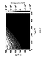
- FIG. 6 is a graph showing the surface energy contribution of Ag (squares) and Cu (circles) nanoparticles as a function of surface area. Calculated values are shown as squares and fits are shown as solid lines.
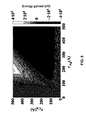
- FIG. 7 is a graph showing the energy gained (eV) from formation of a core/shell structure plotted as a function of the initial (i.e., unjoined) particle radii.
- FIG. 8 is a graph showing the energy gained (eV) from formation of a core/shell structure including estimates of the effects of fractional shell coverage.
- Nanoparticles are characterized by small volumes and a large number of surface atoms, which inherently possess a significantly larger mobility than bulk atoms.
- novel structures, physical properties, and processes can occur with NPs that are not observed for their bulk counterparts. See J. Gleiter, Acta Mater. 48, 1 (2000); F. Delogu et al., Phys. Rev. B 78, 024103 (2008); R. Ferrando et al., Chem. Rev. 108, 845 (2008); and A. Aguado and J. M. Lopez, J. Chem. Phys. 135, 134305 (2011).
- the melting point of a metallic NP is typically lower than that of the bulk metal. See V. Levitas and K. Samani, Nature Communications 2011, DOI: 10.1038/ncomms1275; P. Puri and V. Yang, J. Phys. Chem. C 111, 11776 (2007); and S. L. Lai et al., Appl. Phys. Lett. 72, 1098 (1998).
- the present invention is directed to a nanosolder comprising a first metal nanoparticle core coated with a second metal shell, wherein the first metal has a higher surface energy and/or smaller atomic size than the second metal, and a method for forming such nanosolders comprising heating a mixture of the two metal nanoparticles to a sufficiently high temperature to cause the nanoparticles to react to form the nanosolder.
- the metal nanoparticles can typically be about 5-80 nm in diameter. Simulations suggest that two metal nanoparticles having a wetting angle between them of less than about 50 degrees will form a core/shell structure.
- Cu ( ⁇ 12 nm) and Ag NPs ( ⁇ 6 nm) were thermally reacted and the reaction processes and products were observed using in situ scanning transmission electron microscopy (STEM).
- STEM in situ scanning transmission electron microscopy
- the formation of a three-dimensional (3-D), mainly cube-on-cube epitaxial Cu-core and Ag-shell bimetallic structure was observed during thermal interaction of Cu and Ag NPs at temperatures as low as 150° C.
- the structure was formed by the Ag NPs initially wetting the Cu NP along its ⁇ 111 ⁇ surfaces at multiple locations, forming epitaxial Ag/Cu (111) interfaces, and subsequently Ag atoms diffusing along the Cu surface until the shell was complete. Results were compared to Monte Carlo and MD simulations to understand the stability of the structure and provide insight into the driving force(s) for the formation process.
- in situ electron microscopy is performed in transmission electron microscopy (TEM) mode, which offers the ability to observe the process in real-time.
- TEM transmission electron microscopy
- exposure to the beam for as little as 60 sec rendered the NPs inactive. This change in reactivity is likely due to the formation of a carbon shell around the NPs, similar to that found on Au NPs under electron irradiation by Sutter et al. See E. Sutter et al., Nano Letters 5, 2092 (2005).
- the in situ heating experiments were performed with the electron beam off or with the electron beam on only for the period necessary to obtain the STEM images (typically, less than 30 sec).
- the in situ experiment was performed in STEM mode to facilitate direct identification of Cu and Ag NPs based on high-angle annular dark-field (HAADF) Z-contrast imaging; in this imaging mode the contrast of Ag is brighter relative to Cu due to its higher atomic number.
- HAADF high-angle annular dark-field
- the TEM specimen was made by pre-mixing the NPs in toluene and placing a drop of the mixed solution on a thin carbon film ( ⁇ 5 nm) supported by the TEM grid.
- a thin carbon film ⁇ 5 nm
- Cu and Ag NPs could be assembled on the carbon film such that a monolayer of NPs was formed.
- the larger Cu and smaller Ag NPs are well mixed, with the smaller Ag NPs present in between and in contact with Cu NPs. This intimate contact is critical for initiating the Cu—Ag reaction, since there is a competitive, low temperature Ag—Ag reaction that also takes place during heating.
- FIG. 1( a ) shows a high-resolution HAADF image of the core-shell structure formed at 150° C. with a Cu-core of ⁇ 9 nm in diameter (marked by the circle) and Ag-shell thickness of ⁇ 3 nm.
- the core-shell structure can be clearly discerned due to use of Z-contrast in the HAADF imaging in FIG. 1( a ) .
- the structure was further confirmed by an EDS element map, as shown in FIG. 1( b ) , and an EDS line-profile across the particles, as shown in FIG. 1( c ) .
- the EDS map in FIG. 1( b ) reveals a particle with a somewhat different shape than that observed in FIG. 1( a ) . This is due to the continuously changing Ag-shell that evolves when exposed to inherent electron beam irradiation during EDS acquisition.
- the composition of the Ag shell was determined by EDS quantification from an area marked by a small circle in FIG. 1( b ) where there is no overlapping with the neighboring Cu particles. Within the EDS detection limit of about 1%, the shell was determined to be pure Ag.
- the FFT image from the particle (shown in inset in FIG. 1( a ) ) reveals that the Ag shell forms predominately in a cube-on-cube orientation relationship with the Cu core, or variants of the orientation relationship related by (111) twinning.
- Stacking faults and twin-boundaries are present in parts of the Ag shell, as marked by arrows in FIG. 1( a ) .
- the moiré fringes in FIG. 1( a ) show overlap between Ag and Cu atoms in the electron beam direction, indicating that the Ag is present on the top and/or bottom surface(s) of the Cu core.
- FIGS. 2( a )-( d ) A series of HAADF images showing the process of the core-shell particle formation during heating are shown in FIGS. 2( a )-( d ) .
- FIG. 2( a ) shows a particle with a core-shell structure that has partially formed. It can be observed that an additional Ag NP (marked by a dashed circle near the top of the image) has started to become part of the Ag shell but has not completely merged. Continuous heating at 150° C. for ⁇ 3 min leads to a particle with a more fully formed core-shell structure, as shown in FIG. 2( b ) . Further heating for an additional 3 min gives rise to the final core-shell structure, as shown in FIG. 2( c ) .
- FIG. 2( a ) to FIG. 2( c ) show the moiré fringes at the Cu core as can be clearly observed from FIG. 2( a ) to FIG. 2( c ) , indicating that the Ag has gradually enveloped the Cu-core.
- the Cu—Ag core-shell structure shown in FIG. 2( c ) appears to be stable as long as it stays isolated and no new reactions are initiated with neighboring particles.
- FIG. 2( d ) shows the particle after an additional 7 min of in situ heating at 150° C. As can be observed, with the continued heating the Ag shell began new interactions with the Cu particles to its right and in the lower-right corner.
- the initial Cu—Ag NP reaction involves Ag wetting on Cu surfaces, thereby forming predominately Ag ⁇ 111 ⁇ /Cu ⁇ 111 ⁇ interfaces.
- FIG. 3 shows the initial structure of the reaction between Cu and Ag NPs at 200° C.
- the Ag which has a brighter contrast in the HAADF image, has wet several Cu NPs in multiple locations as marked by arrows in the image.
- the inset image in FIG. 3 shows that a sharp Ag ⁇ 111 ⁇ /Cu ⁇ 111 ⁇ epitaxial interface is formed between the Ag surface layers (as thin as 2-3 ⁇ 111 ⁇ monolayers) and the Cu.
- the lattice spacing measured from the brighter Ag layer is about 0.236 nm, consistent with pure Ag. This observation indicates that the miscibility gap was likely still present for the nanoalloy system, as even a few monolayers of Ag remain segregated at the surface. Note several Ag NPs can wet a single Cu NP at multiple locations. Since the epitaxial Ag/Cu (111) interfaces have several orientation variants, the twins are often formed between different parts of Ag shell, as shown in FIG. 1( a ) , when several Ag NPs involving with interaction with a single Cu NP merge into a single Ag shell.
- the formation of the core-shell structure was studied from a surface energy perspective, with examples elucidating the optimal sizes from both Monte Carlo (MC) and molecular dynamics (MD) simulations.
- the results of these simulations were fitted to simple forms, which were then used to develop a phenomenological model of the energetics of the core-shell structure.
- the energy gained upon formation of this structure was examined as a function of the radii of the two initial nanoparticles to guide synthesis efforts.
- phase diagram of AgCu binary alloys is a simple eutectic, with a eutectic temperature of 1053 K; however, the EAM potential used underestimates this temperature as 935 K. See P. L. Williams et al., Mater. Sci. Eng. 14, 817 (2006).
- the goal was to increase the temperature as high as is feasible for increased diffusion, while remaining below the eutectic line.
- Initial simulations at 723 K indicated that the initial formation of the core-shell structure occurred rapidly but progression to a final equilibrium structure was excessively slow. Therefore the results of the core-shell formation that were run are presented at a temperature of 923 K.
- MC simulations were performed with an in-house code, in which Metropolis moves were accomplished by particle swaps with an additional random translation of up to 0.2 ⁇ in any direction.
- the temperature of the MC simulations was set at 800 K, which was somewhat lower than what was used in the MD models. These results were compared to those at higher temperatures, and while no qualitative difference at 923 K (i.e., the temperature of the MD simulations) could be elucidated, runs at 1200 K (far above the eutectic temperature) showed complete melting and mixing of the system. Therefore, the 800 K MC results represent the structures found at temperatures below the eutectic, without the necessity of using as high a temperature as is feasible, as is the case for the MD simulations. The results are qualitatively similar as there are no structural changes or phase transformations in this region of the phase diagram. Runs were continued until visual inspection indicated an obvious trajectory towards a final state, although these simulations could not establish an equilibrium structure.
- FIGS. 4( a )-( c ) Selected snapshots of the simulation results over time are shown in FIGS. 4( a )-( c ) .
- Runs for the MD calculations began with a 5 nm particle of Ag and Cu that were touching at a single interface along the (010) face.
- FIG. 4( a ) shows the particles in contact (Ag sphere is on the right and Cu sphere is on the left), after energy minimization, prior to dynamics.
- the slow formation of the Ag shell essentially moves the time scale out of the range of MD simulations, even at the elevated temperatures employed. Therefore, MC simulations were investigated to arrive at a better picture of the ending state.
- the MC code used performs random particle swaps (in this case, attempting to exchange Cu for Ag atoms at each MC step) with a small ( ⁇ 0.2 ⁇ ), random translation. Therefore, the process of changing the initial shape of the structure (e.g., from two spherical particles as in the MD simulations to a single spherical core-shell structure) would be exceedingly slow.
- a spherical structure in which one side was composed entirely of Cu atoms and the other entirely of Ag atoms, was used and is hereafter referred to as a janus-NP.
- the results from the MC simulations are shown in FIGS. 5( a )-( c ) .
- the initial janus-NP consists of a particle with a radius of 5 nm that is divided spatially which results in an unequal number of Ag and Cu atoms.
- FIGS. 5( b ) and 5( c ) show the state of the simulation. Note: this is not a true intermediate state as in MD simulations but rather a snapshot of what the preferred final configuration was trending towards.
- the preferred mechanism is to have the Ag atoms move from core positions to the shell, while Cu atoms move into the core. As the simulation progressed, fewer Ag atoms were present in the “core” region and progress towards the final state became asymptotically slower. While these simulations have not yet reached an equilibrium structure, the lowest energy state can be unambiguously identified as the Cu—Ag core-shell structure. Simulation methods exist that can further push this system towards a true energetic minimum. See R.
- E slab N*E coh +2 A ⁇ s (1)
- E slab is the total (minimized) energy of the slab
- N is the number of atoms
- E coh is the cohesive energy
- A is the cross-sectional area
- ⁇ s is the surface energy
- r m is the radius of the nanoparticle
- ⁇ m the number density of the metal m
- a m is the surface area of the nanoparticle.
- N is written in terms of the density of the element and the volume of the particle
- Eq. 7 ensures that the surface and interfacial energies in Eq. 5 are independent of the surface area.
- the values of ⁇ sphere can be determined by calculating the energy of nanoparticles, using Eq. 3 to eliminate the contribution from the cohesive energy, and fitting the data as a function of nanoparticle radius. Fits for Ag and Cu nanoparticles are shown in FIG.
- the final parameter necessary for Eq. 5 is the interfacial energy ⁇ sphere (AgCu) between the Cu core and the Ag shell.
- ⁇ sphere AgCu
- these particles have a variety of exposed surface textures, since the bulk single crystal is oriented with the x, y, and z axes aligned along the [100], [010] and [001] directions, respectively.
- ⁇ CuAg The calculation of a universal value for ⁇ CuAg is difficult, as smaller radii Cu cores lead to a contribution from curvature, while smaller Ag NPs lead to a dependence on the final shell thickness. While these contributions should be negligible given large enough initial particles, these calculations show that ⁇ sphere (AgCu) ranges from about 0.70-0.74 J/m 2 (0.044-0.046 eV/A 2 ). These calculated values of ⁇ sphere (AgCu) are higher than, but comparable to the largest value shown in Table 1, as discussed above for the values of ⁇ sphere (Ag) and ⁇ sphere (Cu).
- E gain E c/s ⁇ E 2
- E gain [ ⁇ shell (Ag) A Ag shell ⁇ sphere (Ag) A Ag NP ]+[ ⁇ sphere (AgCu) A Cu ⁇ sphere (Cu) A Cu NP (9)
- ⁇ shell and ⁇ sphere refer to the surface energies in the shell and original spherical geometry, respectively.
- FIG. 7 A contour plot of the calculated E gain is shown in FIG. 7 .
- the plot shows that the ideal choice for core-shell formation is to utilize relatively small Cu particles as the core with larger Ag particles to act as a shell.
- the energy gained increases (i.e., becomes more negative) as r Ag increases.
- this plot is less accurate when either r Cu is small (due to curvature effects in the surface energies) or r Ag is small (because of incomplete shell formation; see discussion below).
- the first bracketed term representing the difference in the Ag surface energy upon forming a shell from a separate NP
- the second bracketed term is the difference between the Ag/Cu interfacial energy and the surface energy of a bare Cu NP.
- the first term increases with increasing r Cu .
- the reason for this lies in the difference in the outer radius of a core-shell as compared to a bare particle.
- the radius of a core-shell is (r Ag 3 +r Cu 3 ) 1/3 , indicating that as r Cu becomes larger (compared to r Ag ) the final core-shell radius remains close to that of the initial Cu NP.
- Eq. 9 It is possible to modify Eq. 9 to include a correction factor for incomplete coverage.
- a contour plot of the modified energy is shown in FIG. 8 , in which many of the erroneous effects of fractional coverage (specifically when r Ag ⁇ r Cu ) are removed, indicating an energetic gain for most combinations of radii.
- This model demonstrates the formation of a core/shell structure from initially distinct particles, rather than through a co-deposition process, as has been demonstrated previously.
- the model can be useful both for directing synthesis routes for nanoparticles, as well as for choosing specific metallic species which are more or less likely to form such core/shell structures, depending on the desired use. Therefore, although the exemplary observations were limited to the Cu—Ag system, a similar formation process and equilibrium core-shell structure can be expected to extend to other bimetallic and polymetallic systems where metal NPs with different atomic sizes and differing surface energies are thermally interacted.
- the core metal can have a surface energy that is 1.25 times the surface energy of the shell metal.
- the nanosolder can further comprise a polymetallic system comprising three or more different metal nanoparticles and/or nanoparticles comprising metal alloys.
- the nanosolder provides the opportunity to form a solder joint at low process temperatures because the metal nanoparticles melt at temperatures well below the melting temperature of the corresponding bulk materials having the same composition. Once these nanoparticles have melted, the alloy transitions into its bulk counterpart form, being characterized by the higher melting temperature, and consequently solidifies into the final joint.
- the higher melting temperature provides the added margin for the joint to successfully perform at higher service temperatures than the initial, nanosolder melting (process) temperature. The rapidity of this transition also minimizes the detrimental effects of long-term exposure between a molten solder and the base materials, including erosion/dissolution of the latter as well as the formation of brittle intermetallic compounds at the solder/base material interface.
Landscapes
- Engineering & Computer Science (AREA)
- Mechanical Engineering (AREA)
- Powder Metallurgy (AREA)
Abstract
Description
E slab =N*E coh+2Aγ s (1)
where Eslab is the total (minimized) energy of the slab, N is the number of atoms, Ecoh is the cohesive energy, A is the cross-sectional area and γs is the surface energy. The cohesive energy was calculated from an energy minimization of a 500 atom cube (with periodic boundary conditions in all three dimensions) of the individual components. Based on these calculations, the cohesive energies were found to be −2.85 eV/atom for Ag and −3.54 eV/atom for Cu, which are in agreement with literature values. See P. L. Williams et al., Modelling Simul. Mater. Sci. Eng. 14, 817 (2006); and Y. Mishin et al., Phys. Rev. B 63, 224106 (2001). The various combinations of the Ag/Cu surfaces were then put into contact and the interfacial energies calculated using Eq. 2:
E=N(Ag)*E coh(Ag)+A slabγs(Ag)+N(Cu)*E coh(Cu)+A slabγs(Cu)+A slabγCuAg (2)
| TABLE 1 |
| Interfacial and surface energies of various Ag/Cu slabs calculated |
| through Eqs. 1 and 2. |
| γ (J/m2) | Cu{100} | Cu{111} | Surface γAg | ||
| Ag{100} | 0.5323 | 0.4331 | 0.9401 | ||
| Ag{111} | 0.4752 | 0.1970 | 0.8621 | ||
| Surface γCu | 1.3452 | 1.2392 | |||
| 1P. L. Williams et al., Modelling Simul. Mater. Sci. Eng. 14, 817 (2006). | |||||
| 2Y. Mishin et al., Phys. Rev. B 63, 224106 (2001). | |||||
E sphere =N*E coh Aγ sphere (3)
with A being the surface area of the sphere (see Eq. 7), and γsphere being the surface energy of the spherical particle. This surface energy is different from γs in Eqs. 1 and 2 because of the variety of exposed faces in the sphere. The energy for two non-interacting nanoparticles is given by Eq. 4.
E 2 =E sphere(Ag)+E sphere(Cu) (4)
E c/s =N(Ag)*E coh(Ag)+A Agγshell(Ag)+N(Cu)*E coh(Cu)+A Cuγsphere(AgCu) (5)
N=4/3πr 3ρm (6)
A m=4πr m 2 (7)
E gain =E c/s −E 2 (8)
E gain=[γshell(Ag)A Ag shell−γsphere(Ag)A Ag NP]+[γsphere(AgCu)A Cu−γsphere(Cu)A Cu NP (9)
where γshell and γsphere refer to the surface energies in the shell and original spherical geometry, respectively. Since γsphere(CU) is always larger than γsphere(AgCu), the second component of Eq. 9 should be negative (see below). This last statement justifies the selection of the largest values of γsphere(AgCu); larger values will lead to an upper bound of Egain.
r shell=(r Ag 3 +r Cu 3)1/3 −r Cu (10)
which indicates that for most cases with rAg<rCu the shell will be incomplete (i.e., the thickness is less than the size of a Ag atom), and thus
f=r shell√2αAg (11)
where αAg is the lattice constant of Ag, and the √2 estimates the spacing between neighboring {111} layers. This factor modifies Eq. 9 to be
E gain =fγ shell(Ag)A Ag shell−γsphere(Ag)A Ag NP+(1−f)γsphere(Cu)A C +fγ sphere(AgCu)A Cu−γsphere(Cu)A Cu (12)
in the cases where f≦1.0 only; when f=1.0 Eq. 12 reduces to Eq. 9. A contour plot of the modified energy is shown in
Claims (4)
Priority Applications (1)
| Application Number | Priority Date | Filing Date | Title |
|---|---|---|---|
| US14/875,468 US9463532B2 (en) | 2014-03-20 | 2015-10-05 | Low-temperature nanosolders |
Applications Claiming Priority (3)
| Application Number | Priority Date | Filing Date | Title |
|---|---|---|---|
| US201461955906P | 2014-03-20 | 2014-03-20 | |
| US201514660707A | 2015-03-17 | 2015-03-17 | |
| US14/875,468 US9463532B2 (en) | 2014-03-20 | 2015-10-05 | Low-temperature nanosolders |
Related Parent Applications (1)
| Application Number | Title | Priority Date | Filing Date |
|---|---|---|---|
| US201514660707A Continuation-In-Part | 2014-03-20 | 2015-03-17 |
Publications (2)
| Publication Number | Publication Date |
|---|---|
| US20160023308A1 US20160023308A1 (en) | 2016-01-28 |
| US9463532B2 true US9463532B2 (en) | 2016-10-11 |
Family
ID=55165970
Family Applications (1)
| Application Number | Title | Priority Date | Filing Date |
|---|---|---|---|
| US14/875,468 Active US9463532B2 (en) | 2014-03-20 | 2015-10-05 | Low-temperature nanosolders |
Country Status (1)
| Country | Link |
|---|---|
| US (1) | US9463532B2 (en) |
Cited By (4)
| Publication number | Priority date | Publication date | Assignee | Title |
|---|---|---|---|---|
| US9863243B1 (en) | 2015-04-28 | 2018-01-09 | National Technology & Engineering Solutions Of Sandia, Llc | Ruggedized downhole tool for real-time measurements and uses thereof |
| CN109664048A (en) * | 2018-12-30 | 2019-04-23 | 北京康普锡威科技有限公司 | Preparation method, Nanometer Copper cream and its application of Nanometer Copper cream |
| US10763000B1 (en) | 2017-05-03 | 2020-09-01 | National Technology & Engineering Solutions Of Sandia, Llc | Stable nanocrystalline metal alloy coatings with ultra-low wear |
| US10941485B2 (en) | 2018-05-21 | 2021-03-09 | National Technology & Engineering Solutions Of Sandia, Llc | Diamond-like carbon films and uses thereof |
Families Citing this family (3)
| Publication number | Priority date | Publication date | Assignee | Title |
|---|---|---|---|---|
| CN105345314B (en) * | 2015-08-21 | 2017-09-29 | 江苏广昇新材料有限公司 | A kind of high-accuracy nanometer solder(ing) paste scaling powder |
| CN109664049B (en) * | 2019-01-14 | 2021-03-26 | 哈尔滨理工大学 | A kind of multi-scale micro-nano particle composite solder paste for electronic packaging field and preparation method thereof |
| CN112756841B (en) * | 2020-12-25 | 2022-06-03 | 哈尔滨工业大学(深圳) | Micro-nano composite silver-copper alloy soldering paste for low-temperature sintering interconnection and preparation method |
Citations (4)
| Publication number | Priority date | Publication date | Assignee | Title |
|---|---|---|---|---|
| US5439639A (en) * | 1994-01-05 | 1995-08-08 | Sandia Corporation | Tin-silver-bismuth solders for electronics assembly |
| US20060068216A1 (en) * | 2004-09-30 | 2006-03-30 | Fay Hua | Nano-sized metals and alloys, and methods of assembling packages containing same |
| US20070212562A1 (en) * | 2006-02-24 | 2007-09-13 | Samsung Electro-Mecanics Co., Ltd. | Core-shell structure metal nanoparticles and its manufacturing method |
| US7998239B1 (en) * | 2008-11-20 | 2011-08-16 | Sandia Corporation | Alloy nanoparticle synthesis using ionizing radiation |
-
2015
- 2015-10-05 US US14/875,468 patent/US9463532B2/en active Active
Patent Citations (4)
| Publication number | Priority date | Publication date | Assignee | Title |
|---|---|---|---|---|
| US5439639A (en) * | 1994-01-05 | 1995-08-08 | Sandia Corporation | Tin-silver-bismuth solders for electronics assembly |
| US20060068216A1 (en) * | 2004-09-30 | 2006-03-30 | Fay Hua | Nano-sized metals and alloys, and methods of assembling packages containing same |
| US20070212562A1 (en) * | 2006-02-24 | 2007-09-13 | Samsung Electro-Mecanics Co., Ltd. | Core-shell structure metal nanoparticles and its manufacturing method |
| US7998239B1 (en) * | 2008-11-20 | 2011-08-16 | Sandia Corporation | Alloy nanoparticle synthesis using ionizing radiation |
Non-Patent Citations (8)
| Title |
|---|
| Bunge, S. D. et al., "Synthesis of Coinage-Metal Nanoparticles from Mesityl Precursors", Nano Letters, 2003, pp. 901-905, vol. 3. |
| Delogu, F. et al., "Numerical Investigation of the Stability of Ag-Cu Nanorods and Nanowires", Physical Review B, 2008, pp. 024103-1-024103-13, vol. 78. |
| Ferrando, R. et al., "Nanoalloys: From Theory to Applications of Alloy Clusters and Nanoparticles", Chemical Reviews, 2008, pp. 845-910, vol. 108. |
| Rapallo, A. et al., "Global Optimization of Bimetallic Cluster Structures. I. Size-Mismatched Ag-Cu, Ag-, and Au-Cu Systems", The Journal of Chemical Physics, 2005, pp. 194308-1-194308-13, vol. 122. |
| Schick, M. et al., "Investigation of thin Ag/Cu-Alloy Films on Ru(0001)", Journal of Vacuum Science & Technology A, 1994, pp. 1795-1799, vol. 12. |
| Tchaplyguine, M. et al., "Core-Shell Structure Disclosed in Self-Assembled Cu-Ag Nanoalloy Particles", The Journal of Chemical Physics, 2013, pp. 14303-1-14303-6, vol. 138. |
| Yang, J. et al., "Diffusion and Growth of Nickel, Iron and Magnesium Adatoms on the Aluminum Truncated Octahedron: A Molecular Dynamics Simulation", Surface Science, 2012, pp. 971-980, vol. 606. |
| Yang, J. et al., "Substrate Dependence of Growth Configurations for Co-Cu Bimetallic Clusters", Crystal Growth & Design, 2012, pp. 2978-2985, vol. 12. |
Cited By (4)
| Publication number | Priority date | Publication date | Assignee | Title |
|---|---|---|---|---|
| US9863243B1 (en) | 2015-04-28 | 2018-01-09 | National Technology & Engineering Solutions Of Sandia, Llc | Ruggedized downhole tool for real-time measurements and uses thereof |
| US10763000B1 (en) | 2017-05-03 | 2020-09-01 | National Technology & Engineering Solutions Of Sandia, Llc | Stable nanocrystalline metal alloy coatings with ultra-low wear |
| US10941485B2 (en) | 2018-05-21 | 2021-03-09 | National Technology & Engineering Solutions Of Sandia, Llc | Diamond-like carbon films and uses thereof |
| CN109664048A (en) * | 2018-12-30 | 2019-04-23 | 北京康普锡威科技有限公司 | Preparation method, Nanometer Copper cream and its application of Nanometer Copper cream |
Also Published As
| Publication number | Publication date |
|---|---|
| US20160023308A1 (en) | 2016-01-28 |
Similar Documents
| Publication | Publication Date | Title |
|---|---|---|
| US9463532B2 (en) | Low-temperature nanosolders | |
| Grammatikopoulos et al. | Computational modeling of nanoparticle coalescence | |
| Roy et al. | Effect of size, morphology, and synthesis method on the thermal and sintering properties of copper nanoparticles for use in microscale additive manufacturing processes | |
| Meltzman et al. | The equilibrium crystal shape of nickel | |
| He et al. | Nanocrystalline copper for direct copper-to-copper bonding with improved cross-interface formation at low thermal budget | |
| Bin | Size-dependent melting properties of Sn nanoparticles by chemical reduction synthesis | |
| Confalonieri et al. | Al-Sn miscibility gap alloy produced by power bed laser melting for application as phase change material | |
| Meena et al. | Nanophase segregation of self-assembled monolayers on gold nanoparticles | |
| Eckold et al. | The surface energies of β-Sn—A new concept for corrosion and whisker mitigation | |
| Xie et al. | Interfacial diffusion and Kirkendall voids evolution in the Copper-Zinc alloy binary interface revealed by in situ transmission electron microscopy | |
| Zhang et al. | Highly stable nanoscale amorphous microstructure at steel-aluminum interface enabled by a new solid-state additive manufacturing method | |
| Amiri et al. | Insights into formation and growth of colloidal multielement alloy nanoparticles in solution through in situ liquid cell TEM study | |
| Cui et al. | Direct observation of cation diffusion driven surface reconstruction at van der Waals gaps | |
| Zou et al. | Atomic-scale phase separation induced clustering of solute atoms | |
| Wang et al. | Controllable synthesis of platinum diselenide (PtSe 2) inorganic fullerene | |
| Pedrazzini et al. | Effect of substrate bed temperature on solute segregation and mechanical properties in Ti–6Al–4V produced by laser powder bed fusion | |
| Kiani et al. | Dislocation surface nucleation in surfactant-passivated metallic nanocubes | |
| Wang et al. | Effect of Al0. 3CoFeNi content on microstructure, corrosion resistance, and friction performance of aluminium bronze coatings | |
| Zhang et al. | Isothermal solidification for high-entropy alloy synthesis | |
| Yakymovych et al. | Dynamic viscosity of a liquid Sn-3.0 Ag-0.5 Cu alloy with Ni nanoparticles | |
| Yakymovych et al. | Microstructure and electro-physical properties of Sn-3.0 Ag-0.5 Cu nanocomposite solder reinforced with Ni nanoparticles in the melting-solidification temperature range | |
| Li et al. | Grain size effects on interfacial reactions in Fe-Co alloy barrier micro-bumps | |
| Sun et al. | Microstructural stability, defect structures and deformation mechanisms in a Ag3Sn/Cu3Sn alloy | |
| Yang et al. | The synergistic inhibition of the growth of intermetallic compounds at Sn-0.7 Cu/Cu interface by Al and Pt | |
| Barik et al. | Bubble formation and growth during Transient Liquid Phase Bonding in Cu/SnAg system for microelectronic packaging |
Legal Events
| Date | Code | Title | Description |
|---|---|---|---|
| AS | Assignment |
Owner name: SANDIA CORPORATION, NEW MEXICO Free format text: ASSIGNMENT OF ASSIGNORS INTEREST;ASSIGNORS:BOYLE, TIMOTHY J.;LU, PING;VIANCO, PAUL T.;AND OTHERS;REEL/FRAME:036995/0499 Effective date: 20151105 |
|
| STCF | Information on status: patent grant |
Free format text: PATENTED CASE |
|
| AS | Assignment |
Owner name: NATIONAL TECHNOLOGY & ENGINEERING SOLUTIONS OF SAN Free format text: CHANGE OF NAME;ASSIGNOR:SANDIA CORPORATION;REEL/FRAME:047052/0192 Effective date: 20170501 |
|
| MAFP | Maintenance fee payment |
Free format text: PAYMENT OF MAINTENANCE FEE, 4TH YEAR, LARGE ENTITY (ORIGINAL EVENT CODE: M1551); ENTITY STATUS OF PATENT OWNER: LARGE ENTITY Year of fee payment: 4 |
|
| MAFP | Maintenance fee payment |
Free format text: PAYMENT OF MAINTENANCE FEE, 8TH YEAR, LARGE ENTITY (ORIGINAL EVENT CODE: M1552); ENTITY STATUS OF PATENT OWNER: LARGE ENTITY Year of fee payment: 8 |