US9461547B2 - Converter circuitry - Google Patents
Converter circuitry Download PDFInfo
- Publication number
- US9461547B2 US9461547B2 US14/201,005 US201414201005A US9461547B2 US 9461547 B2 US9461547 B2 US 9461547B2 US 201414201005 A US201414201005 A US 201414201005A US 9461547 B2 US9461547 B2 US 9461547B2
- Authority
- US
- United States
- Prior art keywords
- converter
- circuitry
- switch circuits
- resonant
- kilohertz
- Prior art date
- Legal status (The legal status is an assumption and is not a legal conclusion. Google has not performed a legal analysis and makes no representation as to the accuracy of the status listed.)
- Active, expires
Links
Images


Classifications
-
- H—ELECTRICITY
- H02—GENERATION; CONVERSION OR DISTRIBUTION OF ELECTRIC POWER
- H02M—APPARATUS FOR CONVERSION BETWEEN AC AND AC, BETWEEN AC AND DC, OR BETWEEN DC AND DC, AND FOR USE WITH MAINS OR SIMILAR POWER SUPPLY SYSTEMS; CONVERSION OF DC OR AC INPUT POWER INTO SURGE OUTPUT POWER; CONTROL OR REGULATION THEREOF
- H02M3/00—Conversion of DC power input into DC power output
- H02M3/22—Conversion of DC power input into DC power output with intermediate conversion into AC
- H02M3/24—Conversion of DC power input into DC power output with intermediate conversion into AC by static converters
- H02M3/28—Conversion of DC power input into DC power output with intermediate conversion into AC by static converters using discharge tubes with control electrode or semiconductor devices with control electrode to produce the intermediate AC
- H02M3/325—Conversion of DC power input into DC power output with intermediate conversion into AC by static converters using discharge tubes with control electrode or semiconductor devices with control electrode to produce the intermediate AC using devices of a triode or a transistor type requiring continuous application of a control signal
- H02M3/335—Conversion of DC power input into DC power output with intermediate conversion into AC by static converters using discharge tubes with control electrode or semiconductor devices with control electrode to produce the intermediate AC using devices of a triode or a transistor type requiring continuous application of a control signal using semiconductor devices only
- H02M3/33507—Conversion of DC power input into DC power output with intermediate conversion into AC by static converters using discharge tubes with control electrode or semiconductor devices with control electrode to produce the intermediate AC using devices of a triode or a transistor type requiring continuous application of a control signal using semiconductor devices only with automatic control of the output voltage or current, e.g. flyback converters
- H02M3/33523—Conversion of DC power input into DC power output with intermediate conversion into AC by static converters using discharge tubes with control electrode or semiconductor devices with control electrode to produce the intermediate AC using devices of a triode or a transistor type requiring continuous application of a control signal using semiconductor devices only with automatic control of the output voltage or current, e.g. flyback converters with galvanic isolation between input and output of both the power stage and the feedback loop
-
- H—ELECTRICITY
- H02—GENERATION; CONVERSION OR DISTRIBUTION OF ELECTRIC POWER
- H02M—APPARATUS FOR CONVERSION BETWEEN AC AND AC, BETWEEN AC AND DC, OR BETWEEN DC AND DC, AND FOR USE WITH MAINS OR SIMILAR POWER SUPPLY SYSTEMS; CONVERSION OF DC OR AC INPUT POWER INTO SURGE OUTPUT POWER; CONTROL OR REGULATION THEREOF
- H02M1/00—Details of apparatus for conversion
- H02M1/08—Circuits specially adapted for the generation of control voltages for semiconductor devices incorporated in static converters
-
- H—ELECTRICITY
- H02—GENERATION; CONVERSION OR DISTRIBUTION OF ELECTRIC POWER
- H02M—APPARATUS FOR CONVERSION BETWEEN AC AND AC, BETWEEN AC AND DC, OR BETWEEN DC AND DC, AND FOR USE WITH MAINS OR SIMILAR POWER SUPPLY SYSTEMS; CONVERSION OF DC OR AC INPUT POWER INTO SURGE OUTPUT POWER; CONTROL OR REGULATION THEREOF
- H02M3/00—Conversion of DC power input into DC power output
- H02M3/01—Resonant DC/DC converters
-
- H—ELECTRICITY
- H02—GENERATION; CONVERSION OR DISTRIBUTION OF ELECTRIC POWER
- H02M—APPARATUS FOR CONVERSION BETWEEN AC AND AC, BETWEEN AC AND DC, OR BETWEEN DC AND DC, AND FOR USE WITH MAINS OR SIMILAR POWER SUPPLY SYSTEMS; CONVERSION OF DC OR AC INPUT POWER INTO SURGE OUTPUT POWER; CONTROL OR REGULATION THEREOF
- H02M3/00—Conversion of DC power input into DC power output
- H02M3/22—Conversion of DC power input into DC power output with intermediate conversion into AC
- H02M3/24—Conversion of DC power input into DC power output with intermediate conversion into AC by static converters
- H02M3/28—Conversion of DC power input into DC power output with intermediate conversion into AC by static converters using discharge tubes with control electrode or semiconductor devices with control electrode to produce the intermediate AC
- H02M3/325—Conversion of DC power input into DC power output with intermediate conversion into AC by static converters using discharge tubes with control electrode or semiconductor devices with control electrode to produce the intermediate AC using devices of a triode or a transistor type requiring continuous application of a control signal
- H02M3/335—Conversion of DC power input into DC power output with intermediate conversion into AC by static converters using discharge tubes with control electrode or semiconductor devices with control electrode to produce the intermediate AC using devices of a triode or a transistor type requiring continuous application of a control signal using semiconductor devices only
- H02M3/3353—Conversion of DC power input into DC power output with intermediate conversion into AC by static converters using discharge tubes with control electrode or semiconductor devices with control electrode to produce the intermediate AC using devices of a triode or a transistor type requiring continuous application of a control signal using semiconductor devices only having at least two simultaneously operating switches on the input side, e.g. "double forward" or "double (switched) flyback" converter
-
- H—ELECTRICITY
- H02—GENERATION; CONVERSION OR DISTRIBUTION OF ELECTRIC POWER
- H02M—APPARATUS FOR CONVERSION BETWEEN AC AND AC, BETWEEN AC AND DC, OR BETWEEN DC AND DC, AND FOR USE WITH MAINS OR SIMILAR POWER SUPPLY SYSTEMS; CONVERSION OF DC OR AC INPUT POWER INTO SURGE OUTPUT POWER; CONTROL OR REGULATION THEREOF
- H02M3/00—Conversion of DC power input into DC power output
- H02M3/22—Conversion of DC power input into DC power output with intermediate conversion into AC
- H02M3/24—Conversion of DC power input into DC power output with intermediate conversion into AC by static converters
- H02M3/28—Conversion of DC power input into DC power output with intermediate conversion into AC by static converters using discharge tubes with control electrode or semiconductor devices with control electrode to produce the intermediate AC
- H02M3/325—Conversion of DC power input into DC power output with intermediate conversion into AC by static converters using discharge tubes with control electrode or semiconductor devices with control electrode to produce the intermediate AC using devices of a triode or a transistor type requiring continuous application of a control signal
- H02M3/335—Conversion of DC power input into DC power output with intermediate conversion into AC by static converters using discharge tubes with control electrode or semiconductor devices with control electrode to produce the intermediate AC using devices of a triode or a transistor type requiring continuous application of a control signal using semiconductor devices only
- H02M3/33569—Conversion of DC power input into DC power output with intermediate conversion into AC by static converters using discharge tubes with control electrode or semiconductor devices with control electrode to produce the intermediate AC using devices of a triode or a transistor type requiring continuous application of a control signal using semiconductor devices only having several active switching elements
- H02M3/33573—Full-bridge at primary side of an isolation transformer
-
- H—ELECTRICITY
- H02—GENERATION; CONVERSION OR DISTRIBUTION OF ELECTRIC POWER
- H02M—APPARATUS FOR CONVERSION BETWEEN AC AND AC, BETWEEN AC AND DC, OR BETWEEN DC AND DC, AND FOR USE WITH MAINS OR SIMILAR POWER SUPPLY SYSTEMS; CONVERSION OF DC OR AC INPUT POWER INTO SURGE OUTPUT POWER; CONTROL OR REGULATION THEREOF
- H02M1/00—Details of apparatus for conversion
- H02M1/0048—Circuits or arrangements for reducing losses
- H02M1/0054—Transistor switching losses
- H02M1/0058—Transistor switching losses by employing soft switching techniques, i.e. commutation of transistors when applied voltage is zero or when current flow is zero
-
- H02M2001/0048—
-
- Y—GENERAL TAGGING OF NEW TECHNOLOGICAL DEVELOPMENTS; GENERAL TAGGING OF CROSS-SECTIONAL TECHNOLOGIES SPANNING OVER SEVERAL SECTIONS OF THE IPC; TECHNICAL SUBJECTS COVERED BY FORMER USPC CROSS-REFERENCE ART COLLECTIONS [XRACs] AND DIGESTS
- Y02—TECHNOLOGIES OR APPLICATIONS FOR MITIGATION OR ADAPTATION AGAINST CLIMATE CHANGE
- Y02B—CLIMATE CHANGE MITIGATION TECHNOLOGIES RELATED TO BUILDINGS, e.g. HOUSING, HOUSE APPLIANCES OR RELATED END-USER APPLICATIONS
- Y02B70/00—Technologies for an efficient end-user side electric power management and consumption
- Y02B70/10—Technologies improving the efficiency by using switched-mode power supplies [SMPS], i.e. efficient power electronics conversion e.g. power factor correction or reduction of losses in power supplies or efficient standby modes
-
- Y02B70/1433—
-
- Y02B70/1483—
Definitions
- the present disclosure relates to converter circuitry.
- the field of power electronics relates to the control and conversion of electric power. Since power may be provided and used in either direct current (DC) or alternating current (AC) formats and at differing voltage or current levels, there is a continuing need for more efficient and cost effective DC-DC converters, AC-DC converters, AC-AC converters, and DC-AC inverters. For many AC-DC, AC-AC, and DC-AC converters and inverters, a DC-DC converter is a core element in the overall system. These devices are used in electric vehicle chargers, telecom power supplies, industrial power supplies, and alternative energy conversion devices.
- the converter bridge includes multiple switch circuits, which are formed with high voltage silicon carbide MOSFETs (metal-oxide-semiconductor field-effect transistors), and are configured to provide a primary current.
- the tank circuitry includes a resonant capacitance, a resonant inductance, and a transformer with a primary, a first secondary, and a second secondary. The tank circuitry is configured to receive the primary current, and the transformer is associated with a magnetizing inductance.
- the resonant frequency of the tank circuitry is greater than about 225 kilohertz as essentially defined by the magnetizing inductance, the resonant capacitance, and the resonant inductance.
- the rectifier circuitry is coupled to the first secondary and the second secondary, and is adapted to provide a rectified output current.
- the converter bridge may use a 2-level architecture that provides zero voltage switching (ZVS) and operates at high power levels.
- ZVS zero voltage switching
- the output power provided by the DC-DC converter may be between about five kilowatts and 20 kilowatts at a high input voltage of between about 650 and 850 volts or higher.
- Efficiency of the DC-DC converter may be between about 97.5% and 99.0% or higher.
- the DC-DC converter may have a power density between about 35 and 45 watts per cubic inch, even in air-cooled embodiments that employ a fan and associated fan circuitry.
- FIG. 1 is a schematic diagram of an exemplary ZVS converter according to a first embodiment.
- FIG. 2 is a timing diagram for the operation of the ZVS converter of FIG. 1 .
- FIGS. 3A through 3I illustrate the current flow through the ZVS converter in light of the timing diagram of FIG. 2 .
- FIG. 4 illustrates an alternative schematic diagram for the ZVS converter according to a second embodiment.
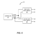
- FIG. 5 is a block diagram of the driver circuitry for the ZVS converter of FIG. 1 according to one embodiment.
- FIG. 6 is a schematic diagram of one of two gate drive circuits of the driver circuitry according to one embodiment.
- FIGS. 7A and 7B illustrate current flow through one part of a gate drive circuit according to one embodiment.
- a full H-bridge, ZVS resonant converter design which is referred to as a zero voltage switching (ZVS) converter 10 .
- the ZVS converter 10 is a two-level architecture and includes a converter bridge 12 , a tank circuitry 14 , rectifier circuitry 16 , filter circuitry 18 , and driver circuitry 20 .
- the ZVS converter 10 is configured to drive a load R L . While the converter bridge 12 is shown as a full H-bridge configuration, those skilled in the art will recognize alternative converter structures.
- the converter bridge 12 includes four switch circuits, which are implemented with four, 1200V N-channel silicon carbide metal-oxide-semiconductor field-effect transistors (MOSFETs) Q 1 -Q 4 . While other material systems, such as gallium nitride (GaN), and transistor types, such as junction field effect transistors (JFETs), may be employed, performance is optimized at this time using silicon carbide MOSFETs. Exemplary MOSFETs include Cree, Inc.'s model number C2M0160120D power MOSFETs. All of the electronics above as well as fan circuitry FN may be provided on a single printed circuit board PCB. The fan circuitry FN includes a fan and related control circuitry to provide forced-air cooling for the electronics of the ZVS converter 10 .
- MOSFETs silicon carbide metal-oxide-semiconductor field-effect transistors
- Each of the transistors Q 1 -Q 4 has an integrated body diode D 1 -D 4 . While the transistors Q 1 -Q 4 have parasitic drain-to-source capacitance, additional capacitors C 1 -C 4 are provided across the drains and sources of the respective transistors Q 1 -Q 4 .
- the transistors Q 1 -Q 4 are arranged as described in the following. Transistors Q 1 and Q 3 are coupled in series between a top rail TR and a bottom rail BR to form a first switch leg, and transistors Q 2 and Q 4 are coupled between the top rail TR and the bottom rail BR to form a second switch leg.
- the second switch leg provides a node A between transistors Q 2 and Q 4
- the first switch leg provides a node B between transistors Q 1 and Q 3 .
- the body diodes D 1 -D 4 are effectively coupled in anti-parallel across the respective transistors Q 1 -Q 4 .
- the primary coil of a transformer T 1 is coupled across nodes A and B.
- the transformer T 1 is illustrated as a non-ideal transformer, and as such, depicts a magnetizing inductance Lm in parallel with the primary coil of the transformer T 1 .
- An additional resonant inductor Lr and a resonant capacitor Cr are coupled in series between node A and the primary coil of the transformer T 1 .
- the secondary coil of the transformer T 1 is center-tapped to provide upper and lower coils.
- a filter capacitor Cf in the filter circuitry 18 and the load R L are shown coupled in parallel with one another across the upper coil.
- a diode DR 1 is coupled is series with the load R L , and in particular, between an upper terminal of the upper coil and a first terminal of the load R L .
- the anode of the diode DR 1 is coupled to the upper terminal of the upper coil, while the cathode is coupled to the first terminal of the load R L .
- the center tap of the transformer T 1 is coupled to the second terminal of the load R L .
- a diode DR 2 is coupled between the bottom terminal of the lower coil of the transformer T 1 and a node C between the cathode of the diode DR 1 and the first terminal of the load R L .
- the anode of the diode DR 2 is coupled to the bottom terminal of the lower coil of the transformer T 1
- the cathode of the diode DR 2 is coupled to Node C.
- the arrangement of the diodes DR 1 , DR 2 represents the rectifier circuitry 16 .
- Diodes DR 1 , DR 2 may, but need not, match the material system of the transistors Q 1 -Q 4 .
- Exemplary silicon carbide diodes for diodes DR 1 , DR 2 are Cree Inc.'s model number C3D16060D diodes.
- control signals S 1 -S 4 are respectively driven by control signals S 1 -S 4 , which are provided by driver circuitry 20 . While each of the control signals S 1 -S 4 may be independent of the others, in the embodiment disclosed below, control signals S 1 and S 4 are either identical or represent the same control signal. Similarly, control signals S 2 and S 3 are either identical or represent the same control signal. As such, transistors Q 1 and Q 4 are turned on and off at the same time, and transistors Q 2 and Q 3 are turned on and off at the same time.
- FIG. 2 a timing diagram is provided to illustrate operation of the ZVS converter 10 .
- the signal Q 2 /Q 3 indicates the state of transistors Q 2 , Q 3
- the signal Q 1 /Q 4 indicates the state of transistors Q 1 , Q 4 .
- a logic high indicates that the corresponding transistors Q 1 -Q 4 are on and conducting, while a logic low indicates that the corresponding transistors Q 1 -Q 4 are off and not conducting.
- the resonant inductor current ILr is the current flowing through the resonant inductor Lr and generally corresponds to a primary current I P that flows through the ZVS converter 10 on the primary side of the transformer T 1 .
- the magnetizing current ILm represents the current flowing through the magnetizing inductance Lm of the transformer T 1 .
- the output current I O represents the secondary current that flows out of node C from either diode DR 1 or diode DR 2 toward the load R L .
- the resonant capacitor voltage VCr is the voltage across the resonant capacitor Cr.
- IQ 1 /IQ 4 is the current flowing through either of transistors Q 1 , Q 4 at any given time.
- a full cycle corresponds to the period t 0 -t 6 .
- the period t 0 -t 3 represents the positive half-cycle of the full cycle, while the period t 3 -t 6 represents the corresponding negative half-cycle of the full cycle.
- transistors Q 1 , Q 4 are turned on and off together, and transistors Q 2 , Q 3 are turned on and off together.
- Transistors Q 1 , Q 4 are never on at the same time as transistors Q 2 , Q 3 , in the illustrated embodiment.
- the magnitude of the resonant inductor current ILr is greater than the magnetizing current ILm.
- the top coil of the transformer T 1 will provide the output current I O to the load R L through the diode DR 1 .
- the magnitude of the magnetizing current ILm is greater than the resonant inductor current ILr.
- the bottom coil of the transformer T 1 will provide the output current I O to the load R L through diode DR 2 . In either half-cycle during the positive and negative half-cycles, the output current I O will also charge the filter capacitor Cf.
- transistors Q 2 , Q 3 are on, and transistors Q 1 , Q 4 are off.
- the primary current I P extends from the top rail TR to the bottom rail BR through transistor Q 2 , node A, resonant inductor Lr, resonant capacitor Cr, the magnetizing inductance Lm, node B, and transistor Q 3 .
- the resonant inductor current ILr and the magnetizing current ILm are negative, and I O is zero.
- the current to the load R L is provided from the filter capacitor Cf, not from either secondary coil of the transformer T 1 .
- An exemplary dead time period is between about 100 ns and 300 ns.
- a complementary dead time is provided for the negative half-cycle at the beginning of period t 3 -t 4 .
- transistors Q 2 , Q 3 turn off and transistors Q 1 , Q 4 remain off for a brief period to provide the dead time.
- the transistors Q 2 , Q 3 turn off, the resonant current ILm continues to flow; however, the primary current I P switches to the path shown in FIG. 3B .
- the primary current I P switches to flow from the bottom rail BR to the top rail TR through the body diode D 4 of transistor Q 4 , node A, the resonant inductor Lr, the resonant capacitor Cr, the primary coil of the transformer T 1 , node B, and body diode D 1 of transistor Q 1 .
- the resonant inductor Lr and the resonant capacitor Cr are in resonance.
- the output current I O begins to flow from the top coil of the transformer T 1 through diode DR 1 to the load R L , as the resonant inductor current ILr further increases above the magnetizing current ILm.
- transistors Q 1 , Q 4 turn on.
- Transistors Q 2 , Q 3 remain off.
- the resonant inductor current ILr continues to flow; however, the path of the primary current I P changes slightly to that shown in FIG. 3C .
- the primary current I P continues to flow from the bottom rail BR to the top rail TR, but no longer flows through the body diode D 4 of transistor Q 4 and the body diode D 1 of transistor Q 1 . Instead, the primary current I P switches to the channels of transistors Q 4 , Q 1 .
- the primary current I F is forced to flow in reverse through the channels of the transistors Q 1 , Q 4 .
- Such operation where current flows in reverse through a MOSFET that is turned on, is referred to as “third quadrant” operation.
- the primary current I P flows from the bottom rail BR to the top rail TR through the channel of transistor Q 4 (instead of the body diode D 4 ), node A, the resonant inductor Lr, the resonant capacitor Cr, the primary coil of the transformer T 1 , node B, and the channel of transistor Q 1 (instead of the body diode D 1 ).
- the output current I O continues to flow from the top coil of the transformer T 1 through diode DR 1 to the load R L , as long as the resonant inductor current ILr remains above the magnetizing current ILm.
- the resonant inductor current ILr will go to zero and allow the primary current I P to reverse direction. As such, the primary current will flow in a forward (or normal direction) through the channels of the transistors Q 1 , Q 4 .
- the primary current I P will flow from the top rail TR to the bottom rail BR through the channel of transistor Q 1 , node B, the primary coil of transformer T 1 , the resonant capacitor Cr, the resonant inductor Lr, node A, and the channel of transistor Q 4 .
- the output current I O continues to flow from the top coil of the transformer T 1 through diode DR 1 to the load R L .
- the resonant current ILr will drop to a level that equals the magnetizing current ILm.
- the output current I O will drop to zero, and thus, current no longer flows through diode DR 1 .
- the current to the load R L is provided by the capacitor Cf.
- the magnetizing inductance Lm, the resonant inductor Lr, and the resonant capacitor Cr resonate to discharge capacitors C 2 , C 3 and charge capacitors C 1 , C 4 for the upcoming negative half-cycle.
- the inductance of the magnetizing inductance Lm is much larger than that of the resonant inductor Lr.
- the magnetizing inductance Lm effectively acts like a constant current source and functions to keep the primary current I P flowing in the same direction and at the same general level throughout period t 2 -t 3 until the transistors Q 1 , Q 4 are turned off at time t 3 .
- the primary current I P will flow from the top rail TR to the bottom rail BR through the channel of transistor Q 1 , node B, the magnetizing inductance Lm of transformer T 1 , the resonant capacitor Cr, the resonant inductor Lr, node A, and the channel of transistor Q 4 .
- the negative half-cycle works in a symmetrical manner to the positive half-cycle. Reference is made to FIGS. 2 and 3F through 3I for illustration. For the sake of conciseness, an extended analysis like that provided for the positive half-cycle is not provided for the negative half-cycle, given the exact symmetry of operation of the positive and negative half-cycles.
- the concepts above may be applied to different converter architectures, which use 2-level or higher configurations, and will result in uniquely small and efficient designs that are capable of operating at switching frequencies much higher than those of silicon-based counterparts.
- silicon carbide components allows a 2-level converter architecture to have a sustained output power of 5 kilowatts to 20 kilowatts, an input voltage of 650 V to 850 V, an overall efficiency rating between 97.5 and 99.0 percent, and a power density between 35 and 45 watts per cubic inch (including the volume of all components and the PCB, or PCBs if multiple PCBs are used).
- the resonant frequency of the tank circuitry 14 may range from 225 kilohertz to 500 kilohertz when providing an output power over 5 kilowatts and an input voltage of greater than 650 V while maintaining an overall efficiency of greater than 97.5 percent.
- the resonant frequency is primarily defined by the values of the magnetizing inductance Lm, the inductance of the resonant inductor Lr, and the capacitance of the resonant capacitor Cr.
- a silicon-based architecture operating at these power levels may only be able to support a resonant frequency in the range of 75 kilohertz to 150 kilohertz.
- the higher resonant frequency allows these resonant components (Lm, Lr, Cr) to have much smaller values, and thus be much smaller in size.
- a first set of parameters may define a 2-level converter architecture that provides a sustained output power of 5 kilowatts to 20 kilowatts, an input voltage of 650 V to 850 V, an overall efficiency rating between 97.5 and 99.0 percent, a power density between 35 and 45 watts per cubic inch, and a resonant frequency for the tank circuitry 14 between 225 kilohertz and 500 kilohertz.
- a second set of parameters may define a 2-level converter architecture that provides a sustained output power of 5 kilowatts to 10 kilowatts, an input voltage of 650 V to 800 V, an overall efficiency rating between 98.0 and 99.0 percent, a power density between 35 and 45 watts per cubic inch, and a resonant frequency for the tank circuitry 14 between 250 kilohertz and 450 kilohertz.
- a third set of parameters may define a 2-level converter architecture that provides a sustained output power greater than 5 kilowatts, an input voltage greater than 650 V, an overall efficiency rating greater than 97.5 percent, a power density greater than 35 watts per cubic inch, and a resonant frequency for the tank circuitry 14 greater than 225 kilohertz.
- each of the four switch circuits is configured with parallel transistors, and in particular, parallel MOSFETs.
- the first switch circuit which resides at the top of the left shunt leg, includes parallel MOSFETs Q 1 ′, Q 1 ′′.
- the respective gates, drains, and sources of MOSFETs Q 1 ′, Q 1 ′′ are directly coupled to one another.
- Each of the MOSFETs Q 1 ′, Q 1 ′′ will include body diodes D 1 ′, D 1 ′′.
- One or more capacitors C 1 may be provided across the drains and sources of the MOSFETs Q 1 ′, Q 1 ′′.
- the second switch circuit which resides in the top of the right shunt leg, includes parallel MOSFETs Q 2 ′, Q 2 ′′.
- the respective gates, drains, and sources of MOSFETs Q 2 ′, Q 2 ′′ are directly coupled to one another.
- Each of the MOSFETs Q 2 ′, Q 2 ′′ will include body diodes D 2 ′, D 2 ′′.
- One or more capacitors C 2 may be provided across the drains and sources of the MOSFETs Q 2 ′, Q 2 ′′.
- the third switch circuit which resides in the bottom of the left shunt leg, includes parallel MOSFETs Q 3 ′, Q 3 ′′.
- MOSFETs Q 3 ′, Q 3 ′′ are directly coupled to one another.
- Each of the MOSFETs Q 3 ′, Q 3 ′′ will include body diodes D 3 ′, D 3 ′′.
- One or more capacitors C 3 may be provided across the drains and sources of the MOSFETs Q 3 ′, Q 3 ′′.
- the fourth switch circuit which resides in the bottom of the right shunt leg, includes parallel MOSFETs Q 4 ′, Q 4 ′′.
- the respective gates, drains, and sources of MOSFETs Q 4 ′, Q 4 ′′ are directly coupled to one another.
- Each of the MOSFETs Q 4 ′, Q 4 ′′ will include body diodes D 4 ′, D 4 ′′.
- One or more capacitors C 4 may be provided across the drains and sources of the MOSFETs Q 4 ′, Q 4 ′′.
- the driver circuitry 20 will include an analog or digital controller 22 , the first gate drive circuit 24 , and a second gate drive circuit 26 , as shown in FIG. 5 .
- the controller 22 will output two input signals, which are referenced as S 1 /S 4 ′ and S 2 /S 3 ′, respectively. Logically, these signals will be the complement of the S 1 /S 4 and S 2 /S 3 transistor states shown in FIG. 2 .
- Each of the two input signals S 1 /S 4 ′, S 2 /S 3 ′ will be provided to both the first gate drive circuit 24 and the second gate drive circuit 26 .
- the first gate drive circuit 24 will process the input signals S 1 /S 4 ′ and S 2 /S 3 ′ and provide control signals S 1 , S 3 , which are used to drive the respective top and bottom switch circuits in the left shunt leg.
- the second gate drive circuit 26 will process the input signals S 1 /S 4 ′ and S 2 /S 3 ′ and provide control signals S 2 , S 4 , which are used to drive the respective top and bottom switch circuits in the right shunt leg.
- FIG. 6 illustrates an exemplary schematic for the first gate drive circuit 24 .
- the second gate drive circuit 26 is configured in an analogous fashion.
- the goal of the first and second gate drive circuits 24 , 26 is to provide control signals S 1 -S 4 , such that a relatively high turn-on voltage is provided to the respective gates to quickly turn on the corresponding transistors Q 1 -Q 4 and negative turnoff voltage is provided to the respective gates to quickly turn off the corresponding transistors Q 1 -Q 4 .
- the turn-on voltage is approximately 20 V
- the turn-off voltage is initially ⁇ 2.4 V before transitioning to or toward 0 V.
- Those skilled in the art will recognize other voltage levels for both the positive turn-on and negative turn-off voltages.
- the first gate drive circuit 24 includes two buffer circuits B 1 , B 2 , which drive the respective terminals of a primary coil for a transformer T 2 .
- input signal S 1 /S 4 ′ is coupled to the top terminal of the primary coil through series connected buffer B 1 , resistor R 1 , and capacitor C 5 .
- Input signal S 2 /S 3 ′ is coupled to the bottom terminal of the primary coil.
- the input signals S 1 /S 4 ′ and S 2 /S 3 ′ are configured such that states S 1 /S 4 are both low during the dead time at the beginning of the period t 0 -t 1 .
- Input signals S 1 /S 4 ′ and S 2 /S 3 ′ are further configured such that states S 1 /S 4 are complementary to each other for the remaining times, such that state S 1 /S 4 is the complement of state S 2 /S 3 at all times other than the dead times.
- the transformer T 2 has two secondary coils, which feed independent top and bottom circuits, respectively.
- the top circuit will provide the control signal S 1
- the bottom circuit will provide the control signal S 3 .
- the top and bottom circuits are identical; however, the secondary coils are connected to the top and bottom circuits with opposite polarity. This will ensure that control signals S 1 , S 3 are never high at the same time and are logically opposite one another for all times, other than the dead time, when input signals S 1 /S 4 ′ and S 2 /S 3 ′ are at the same level.
- the top circuit has a signal rail SR 1 and a return rail RR 1 .
- the signal rail SR 1 is coupled between node D, which corresponds to the bottom terminal of the top secondary coil of transformer T 2 , and node E, which outputs the control signal S 1 .
- the signal rail SR 1 includes series connected diode D 5 and resistor R 2 , wherein node F resides between the diode D 5 and the resistor R 2 .
- a resistor R 3 is coupled across the diode D 5 .
- the return rail RR 1 is coupled between nodes G and H.
- Diode D 6 and Zener diode Z 1 are connected in series along the return rail RR 1 , such that the anodes of the diode D 6 and the Zener diode Z 1 are coupled together at node I.
- Capacitor C 6 is coupled across the Zener diode Z 1 .
- Transistor Q 5 which may be an N-channel MOSFET or NPN bipolar transistor, is coupled between nodes F and I, wherein the gate is coupled to node G.
- Resistor R 4 is coupled between node F and the gate of transistor Q 5 .
- Two shunt circuits are coupled between node F and node H.
- the first shunt circuit includes series connected diode D 7 and resistor R 5 , wherein the anode of diode D 7 is coupled to node F.
- the second shunt circuit includes two series connected Zener diodes Z 2 , Z 3 , which are connected in a blocking manner.
- the anodes of the Zener diodes Z 2 , Z 3 are coupled together, the cathode of Zener diode Z 2 is coupled to node F, and the cathode of Zener diode Z 3 is coupled to node H.
- Resistor R 6 is coupled between nodes E and H.
- the bottom circuit has a signal rail SR 2 and a return rail RR 2 .
- the signal rail SR 2 is coupled between node J, which corresponds to the top terminal of the bottom secondary coil of transformer T 2 , and node K, which outputs the control signal S 3 .
- the signal rail SR 2 includes series connected diode D 8 and resistor R 7 , wherein node L resides between the diode D 8 and the resistor R 7 .
- a resistor R 8 is coupled across the diode D 8 .
- the return rail RR 2 is coupled between nodes M and N.
- Diode D 9 and Zener diode Z 4 are connected in series along the return rail RR 2 , such that the anodes of the diode D 9 and the Zener diode Z 4 are coupled together at node O.
- Capacitor C 7 is coupled across the Zener diode Z 4 .
- Transistor Q 6 which may be an N-channel MOSFET or NPN bipolar transistor, is coupled between nodes L and O, wherein the gate is coupled to node M.
- Resistor R 9 is coupled between node L and the gate of transistor Q 6 .
- Two shunt circuits are coupled between node L and node N.
- the first shunt circuit includes series connected diode D 10 and resistor R 10 , wherein the anode of diode D 10 is coupled to node L.
- the second shunt circuit includes two series connected Zener diodes Z 5 , Z 6 , which are connected in a blocking manner.
- the anodes of the Zener diodes Z 5 , Z 6 are coupled together, the cathode of Zener diode Z 5 is coupled to node L, and the cathode of Zener diode Z 6 is coupled to node N.
- Resistor R 11 is coupled between nodes K and N.
- the semiconductor devices in the first and second gate drive circuits 24 , 26 are silicon-based, while the semiconductor devices in the ZVS converter 10 are silicon carbide-based devices. Those skilled in the art will appreciate that other material systems are available for these semiconductor devices.
- the first gate drive circuit 24 is able to generate control signals S 1 and S 3 , such that the turn-on voltage is 20 V (the silicon carbide MOSFET recommended turn-on voltage) and the turn-off voltage is generally constant at ⁇ 2.4 V before transitioning to or toward 0 V at the dead time.
- the negative turn-off voltage helps to quickly turn off the silicon carbide MOSFETs, and reduces the possibility of noise causing the MOSFTET to errantly turn on during the off state.
- the transformer T 2 is configured to provide a 24 V signal across both secondary coils when the input signals S 1 /S 4 ′, S 2 /S 3 ′ are in complementary states.
- the two input voltages V D and corresponding current paths in the top circuit of the first gate drive circuit 24 are shown for the two corresponding turn-on and turn-off voltages for control signal S 1 .
- the input voltage V D is the voltage across the secondary coil of transformer T 2 .
- the bottom circuit of the first gate drive circuit 24 and both the top and bottom circuits of the second gate drive circuit 26 operate in the same fashion.
- FIG. 7A For the turn-on state, reference is made to FIG. 7A .
- transistor Q 5 When the input voltage V D is positive across nodes D and F, transistor Q 5 is off, and diodes D 5 , D 6 , and D 7 are forward biased. As such, current flows through node D, diode D 5 , to node H where it splits into two branches. The first branch flows through resistor R 2 to node E and represents the control signal S 1 .
- the second branch flows through diode D 7 , resistor R 5 , capacitor C 6 , node I, diode D 6 , to node F.
- capacitor C 6 is charged.
- the charge across capacitor C 6 is limited to 2.4 V by the Zener diode Z 1 .
- the charge across capacitor C 6 is used in the subsequent turn-off state to generate the ⁇ 2.4 V turn-off voltage.
- transistor Q 5 turns on to help with a fast turn-off and diode D 6 blocks current flow to the winding of T 2 .
- capacitor C 6 acts like a voltage source to generate the ⁇ 2.4 V bias for control signal S 1 .
Landscapes
- Engineering & Computer Science (AREA)
- Power Engineering (AREA)
- Dc-Dc Converters (AREA)
Abstract
Description
Claims (25)
Priority Applications (4)
| Application Number | Priority Date | Filing Date | Title |
|---|---|---|---|
| US14/201,005 US9461547B2 (en) | 2014-03-07 | 2014-03-07 | Converter circuitry |
| CN201580012508.6A CN106068606B (en) | 2014-03-07 | 2015-03-04 | Converter circuit |
| PCT/US2015/018741 WO2015134616A1 (en) | 2014-03-07 | 2015-03-04 | Converter circuitry |
| EP15710065.2A EP3114762A1 (en) | 2014-03-07 | 2015-03-04 | Converter circuitry |
Applications Claiming Priority (1)
| Application Number | Priority Date | Filing Date | Title |
|---|---|---|---|
| US14/201,005 US9461547B2 (en) | 2014-03-07 | 2014-03-07 | Converter circuitry |
Publications (2)
| Publication Number | Publication Date |
|---|---|
| US20150256084A1 US20150256084A1 (en) | 2015-09-10 |
| US9461547B2 true US9461547B2 (en) | 2016-10-04 |
Family
ID=52682941
Family Applications (1)
| Application Number | Title | Priority Date | Filing Date |
|---|---|---|---|
| US14/201,005 Active 2034-08-01 US9461547B2 (en) | 2014-03-07 | 2014-03-07 | Converter circuitry |
Country Status (4)
| Country | Link |
|---|---|
| US (1) | US9461547B2 (en) |
| EP (1) | EP3114762A1 (en) |
| CN (1) | CN106068606B (en) |
| WO (1) | WO2015134616A1 (en) |
Cited By (3)
| Publication number | Priority date | Publication date | Assignee | Title |
|---|---|---|---|---|
| US20150311807A1 (en) * | 2014-04-29 | 2015-10-29 | Valeo Equipements Electriques Moteur | Power supply and method for controlling a power supply |
| US20160315557A1 (en) * | 2015-04-23 | 2016-10-27 | Panasonic Intellectual Property Management Co., Ltd. | Power converter |
| US11923716B2 (en) | 2019-09-13 | 2024-03-05 | Milwaukee Electric Tool Corporation | Power converters with wide bandgap semiconductors |
Families Citing this family (14)
| Publication number | Priority date | Publication date | Assignee | Title |
|---|---|---|---|---|
| US9680376B2 (en) | 2014-02-28 | 2017-06-13 | Cree, Inc. | Power conversion electronics having conversion and inverter circuitry |
| CN105141162A (en) * | 2015-10-22 | 2015-12-09 | 保定四方三伊电气有限公司 | Series resonant inverter based on silicon carbide MOSFETs |
| US20180191236A1 (en) * | 2017-01-05 | 2018-07-05 | General Electric Company | Filter Device for Power Converters with Silicon Carbide Mosfets |
| US10579916B2 (en) * | 2017-07-07 | 2020-03-03 | Integrated Device Technology, Inc. | Low power magnetic secure transmission system |
| CN107370378B (en) * | 2017-07-12 | 2019-08-30 | 北京航空航天大学 | A high-power high-voltage DC-DC converter for trolleybus |
| US11264903B2 (en) * | 2017-09-18 | 2022-03-01 | Texas Instruments Incorporated | Power converter with zero-voltage switching |
| CN110868090A (en) * | 2018-08-28 | 2020-03-06 | 中车大同电力机车有限公司 | SiC power module and electric locomotive storage battery charging circuit comprising same |
| JP7133436B2 (en) * | 2018-10-26 | 2022-09-08 | 富士フイルムヘルスケア株式会社 | High voltage equipment and X-ray diagnostic imaging equipment |
| US10666147B1 (en) * | 2018-11-14 | 2020-05-26 | Navitas Semiconductor, Inc. | Resonant converter control based on zero current detection |
| CN109660113A (en) * | 2019-01-16 | 2019-04-19 | 中国科学院空间应用工程与技术中心 | A kind of resonance drive circuit |
| US10938313B2 (en) * | 2019-05-20 | 2021-03-02 | Utah State University | Constant DC current input to constant DC voltage output power supply covering a wide programmable range |
| US11018529B2 (en) | 2019-05-20 | 2021-05-25 | Utah State University | Wireless charger for underwater vehicles fed from a constant current distribution cable |
| CN114785128B (en) * | 2022-04-24 | 2025-12-23 | 华南理工大学 | High-ratio DC/DC converter with wide input voltage range and adjustable gain |
| CN115051571B (en) * | 2022-05-05 | 2025-04-01 | 深圳市科华恒盛科技有限公司 | A bidirectional DC-DC conversion circuit and its control method and charging device |
Citations (17)
| Publication number | Priority date | Publication date | Assignee | Title |
|---|---|---|---|---|
| US5132889A (en) * | 1991-05-15 | 1992-07-21 | Ibm Corporation | Resonant-transition DC-to-DC converter |
| US20080103632A1 (en) | 2006-10-27 | 2008-05-01 | Direct Drive Systems, Inc. | Electromechanical energy conversion systems |
| US20080316780A1 (en) | 2007-06-20 | 2008-12-25 | Vacon Oyj | Limitation of voltage pulse |
| US20100301826A1 (en) | 2009-06-02 | 2010-12-02 | Intersil Americas Inc. | System and method for oring phases to overcome duty cycle limitations in a multi-phase boost converter |
| US20120039092A1 (en) * | 2010-08-13 | 2012-02-16 | Fsp Technology Inc. | Current-input-type parallel resonant dc/dc converter and method thereof |
| US20120126728A1 (en) | 2010-11-19 | 2012-05-24 | El-Refaie Ayman Mohamed Fawzi | Integrated electric machine and silicon carbide power converter assembly and method of making same |
| WO2012090242A1 (en) | 2010-12-27 | 2012-07-05 | 日立アプライアンス株式会社 | Power converter and solar power generation system |
| US20120294045A1 (en) * | 2011-05-19 | 2012-11-22 | Enphase Energy, Inc. | Method and apparatus for controlling resonant converter output power |
| US20120326646A1 (en) | 2010-03-09 | 2012-12-27 | Mitsubishi Electric Corporation | Power semiconductor module, power converting apparatus, and railway car |
| US20130002215A1 (en) | 2010-06-29 | 2013-01-03 | Mitsubishi Electric Corporation | Dc-dc power conversion apparatus |
| US20130063184A1 (en) | 2010-09-09 | 2013-03-14 | Aegis Technology, Inc | High temperature operation silicon carbide gate driver |
| US8477519B2 (en) * | 2010-07-13 | 2013-07-02 | Minebea Co., Ltd | Method for controlling a switching power unit using an AC/DC converter, a power factor correction unit, and a DC/DC converter unit |
| US20140104901A1 (en) | 2012-10-11 | 2014-04-17 | Hamilton Sundstrand Corporation | Emi filtering for active rectifier power systems |
| US20140355313A1 (en) | 2012-02-03 | 2014-12-04 | Fuji Electric Co., Ltd. | Resonant dc-dc converter control device |
| US20150055374A1 (en) * | 2013-08-22 | 2015-02-26 | Fujitsu Telecom Networks Limited | Switching power supply apparatus corresponding to zero voltage switching system |
| US20150098250A1 (en) * | 2013-10-04 | 2015-04-09 | Chicony Power Technology Co., Ltd. | Method of controlling phase-shift full-bridge converter in light load operation |
| US20150249384A1 (en) | 2014-02-28 | 2015-09-03 | Cree, Inc. | Power conversion electronics |
Family Cites Families (6)
| Publication number | Priority date | Publication date | Assignee | Title |
|---|---|---|---|---|
| US5481219A (en) * | 1994-07-20 | 1996-01-02 | At&T Corp. | Apparatus and method for generting negative bias for isolated MOSFET gate-drive circuits |
| US6392902B1 (en) * | 2000-08-31 | 2002-05-21 | Delta Electronics, Inc. | Soft-switched full-bridge converter |
| US6992902B2 (en) * | 2003-08-21 | 2006-01-31 | Delta Electronics, Inc. | Full bridge converter with ZVS via AC feedback |
| JP5157987B2 (en) * | 2009-03-25 | 2013-03-06 | 株式会社豊田自動織機 | Isolated DC-DC converter |
| KR20130043612A (en) * | 2010-02-18 | 2013-04-30 | 페터 발데마르 렌 | Dc-dc converter circuit for high input-to-output voltage conversion |
| EP2445098B1 (en) * | 2010-10-25 | 2019-08-07 | STMicroelectronics Srl | Control device for a resonant converter. |
-
2014
- 2014-03-07 US US14/201,005 patent/US9461547B2/en active Active
-
2015
- 2015-03-04 WO PCT/US2015/018741 patent/WO2015134616A1/en not_active Ceased
- 2015-03-04 EP EP15710065.2A patent/EP3114762A1/en not_active Ceased
- 2015-03-04 CN CN201580012508.6A patent/CN106068606B/en active Active
Patent Citations (18)
| Publication number | Priority date | Publication date | Assignee | Title |
|---|---|---|---|---|
| US5132889A (en) * | 1991-05-15 | 1992-07-21 | Ibm Corporation | Resonant-transition DC-to-DC converter |
| US20080103632A1 (en) | 2006-10-27 | 2008-05-01 | Direct Drive Systems, Inc. | Electromechanical energy conversion systems |
| US20080316780A1 (en) | 2007-06-20 | 2008-12-25 | Vacon Oyj | Limitation of voltage pulse |
| US20100301826A1 (en) | 2009-06-02 | 2010-12-02 | Intersil Americas Inc. | System and method for oring phases to overcome duty cycle limitations in a multi-phase boost converter |
| US20120326646A1 (en) | 2010-03-09 | 2012-12-27 | Mitsubishi Electric Corporation | Power semiconductor module, power converting apparatus, and railway car |
| US20130002215A1 (en) | 2010-06-29 | 2013-01-03 | Mitsubishi Electric Corporation | Dc-dc power conversion apparatus |
| US8477519B2 (en) * | 2010-07-13 | 2013-07-02 | Minebea Co., Ltd | Method for controlling a switching power unit using an AC/DC converter, a power factor correction unit, and a DC/DC converter unit |
| US20120039092A1 (en) * | 2010-08-13 | 2012-02-16 | Fsp Technology Inc. | Current-input-type parallel resonant dc/dc converter and method thereof |
| US20130063184A1 (en) | 2010-09-09 | 2013-03-14 | Aegis Technology, Inc | High temperature operation silicon carbide gate driver |
| US20120126728A1 (en) | 2010-11-19 | 2012-05-24 | El-Refaie Ayman Mohamed Fawzi | Integrated electric machine and silicon carbide power converter assembly and method of making same |
| WO2012090242A1 (en) | 2010-12-27 | 2012-07-05 | 日立アプライアンス株式会社 | Power converter and solar power generation system |
| US20120294045A1 (en) * | 2011-05-19 | 2012-11-22 | Enphase Energy, Inc. | Method and apparatus for controlling resonant converter output power |
| US20140355313A1 (en) | 2012-02-03 | 2014-12-04 | Fuji Electric Co., Ltd. | Resonant dc-dc converter control device |
| EP2811638A1 (en) | 2012-02-03 | 2014-12-10 | Fuji Electric Co., Ltd. | Control device for resonance-type dc-dc converter |
| US20140104901A1 (en) | 2012-10-11 | 2014-04-17 | Hamilton Sundstrand Corporation | Emi filtering for active rectifier power systems |
| US20150055374A1 (en) * | 2013-08-22 | 2015-02-26 | Fujitsu Telecom Networks Limited | Switching power supply apparatus corresponding to zero voltage switching system |
| US20150098250A1 (en) * | 2013-10-04 | 2015-04-09 | Chicony Power Technology Co., Ltd. | Method of controlling phase-shift full-bridge converter in light load operation |
| US20150249384A1 (en) | 2014-02-28 | 2015-09-03 | Cree, Inc. | Power conversion electronics |
Non-Patent Citations (7)
| Title |
|---|
| Burkart, Ralph M. et al., "Comparative Evaluation of SiC and Si PV Inverter Systems Based on Power Density and Efficiency as Indicators of Initial Cost and Operating Revenue," 2013 IEEE 14th Workshop on Control and Modeling for Power Electronics (COMPEL), Jun. 23-26, 2013, IEEE, 6 pages. |
| Deboy, Gerald et al., "New SiC JFET Boost Performance of Solar Inverters," Power Electronics Europe, Issue 4, 2011, Access Intelligence, pp. 29-33. |
| International Search Report and Written Opinion for International Patent Application No. PCT/US2015/017529, mailed Jun. 25, 2015, 20 pages. |
| International Search Report and Written Opinion for International Patent Application No. PCT/US2015/018741, mailed Jun. 3, 2015, 11 pages. |
| Liu, Jimmy et al., "Performance Evaluations of Hard-Switching Interleaved DC/DC Boost Converter with New Generation Silicon Carbide MOSFETs," Aug. 6, 2013, http://www.cree.com/~/media/Files/Cree/Power/Articles%20and%20Papers/Power-Article-4.pdf, Cree, Inc., 6 pages. |
| Liu, Jimmy et al., "Performance Evaluations of Hard-Switching Interleaved DC/DC Boost Converter with New Generation Silicon Carbide MOSFETs," Aug. 6, 2013, http://www.cree.com/˜/media/Files/Cree/Power/Articles%20and%20Papers/Power-Article-4.pdf, Cree, Inc., 6 pages. |
| Non-Final Office Action for U.S. Appl. No. 14/193,842, mailed Jun. 29, 2016, 18 pages. |
Cited By (6)
| Publication number | Priority date | Publication date | Assignee | Title |
|---|---|---|---|---|
| US20150311807A1 (en) * | 2014-04-29 | 2015-10-29 | Valeo Equipements Electriques Moteur | Power supply and method for controlling a power supply |
| US10355597B2 (en) * | 2014-04-29 | 2019-07-16 | Valeo Equipements Electriques Moteur | Power supply and method for controlling a power supply |
| US20160315557A1 (en) * | 2015-04-23 | 2016-10-27 | Panasonic Intellectual Property Management Co., Ltd. | Power converter |
| US9673735B2 (en) * | 2015-04-23 | 2017-06-06 | Panasonic Intellectual Property Management Co., Ltd. | Power converter |
| US11923716B2 (en) | 2019-09-13 | 2024-03-05 | Milwaukee Electric Tool Corporation | Power converters with wide bandgap semiconductors |
| US12341373B2 (en) | 2019-09-13 | 2025-06-24 | Milwaukee Electric Tool Corporation | Power converters with wide bandgap semiconductors |
Also Published As
| Publication number | Publication date |
|---|---|
| US20150256084A1 (en) | 2015-09-10 |
| CN106068606A (en) | 2016-11-02 |
| CN106068606B (en) | 2019-01-04 |
| WO2015134616A1 (en) | 2015-09-11 |
| EP3114762A1 (en) | 2017-01-11 |
Similar Documents
| Publication | Publication Date | Title |
|---|---|---|
| US9461547B2 (en) | Converter circuitry | |
| US8957642B2 (en) | Enhancement mode III-nitride switch with increased efficiency and operating frequency | |
| US9484821B2 (en) | Adjustable resonant apparatus for power converters | |
| US7961482B2 (en) | Bi-directional HEMT/GaN half-bridge circuit | |
| US9812977B2 (en) | Resonant converters with an improved voltage regulation range | |
| US20140153294A1 (en) | AC/DC Power Converter Arrangement | |
| US10686361B2 (en) | Synchronous rectifier gate driver with active clamp | |
| US9112428B2 (en) | Application of normally-on switching elements/devices in a stacked switching circuit | |
| US9991799B2 (en) | Switch mode power supplies including primary side clamping circuits controlled based on secondary side signals | |
| US8018279B2 (en) | Class D amplifier circuit with bi-directional power switch | |
| US20160065064A1 (en) | System and Method for a Switch Having a Normally-on Transistor and a Normally-off Transistor | |
| US20130271187A1 (en) | Driver for semiconductor switch element | |
| US9948289B2 (en) | System and method for a gate driver | |
| TW201717530A (en) | Automatic enhanced self-driven synchronous rectification for power converters | |
| US10256736B2 (en) | DC-DC converter with polarity reversal protection | |
| US9780676B2 (en) | Power converter with a snubber circuit | |
| US9722599B1 (en) | Driver for the high side switch of the cascode switch | |
| KR102005881B1 (en) | DC to DC Converting System | |
| US20220407412A1 (en) | Inverter circuit and method, for example for use in power factor correction | |
| US6859372B2 (en) | Bridge-buck converter with self-driven synchronous rectifiers | |
| JP2014193022A (en) | Switching circuit and power conversion device | |
| US7787265B2 (en) | Self-coupled driver used in dual-switch forward power converter | |
| US10498213B2 (en) | Drive circuit and semiconductor module utilizing a capacitance ratio between different switches | |
| Anthony et al. | A design method for isolated resonant gate drivers | |
| JP5640731B2 (en) | Drive circuit and switching power supply device |
Legal Events
| Date | Code | Title | Description |
|---|---|---|---|
| AS | Assignment |
Owner name: CREE, INC., NORTH CAROLINA Free format text: ASSIGNMENT OF ASSIGNORS INTEREST;ASSIGNORS:LIU, XUECHAO;MOOKKEN, JOHN;REEL/FRAME:032474/0639 Effective date: 20140307 |
|
| STCF | Information on status: patent grant |
Free format text: PATENTED CASE |
|
| CC | Certificate of correction | ||
| MAFP | Maintenance fee payment |
Free format text: PAYMENT OF MAINTENANCE FEE, 4TH YEAR, LARGE ENTITY (ORIGINAL EVENT CODE: M1551); ENTITY STATUS OF PATENT OWNER: LARGE ENTITY Year of fee payment: 4 |
|
| AS | Assignment |
Owner name: WOLFSPEED, INC., NORTH CAROLINA Free format text: CHANGE OF NAME;ASSIGNOR:CREE, INC.;REEL/FRAME:057891/0880 Effective date: 20211001 |
|
| AS | Assignment |
Owner name: U.S. BANK TRUST COMPANY, NATIONAL ASSOCIATION, NORTH CAROLINA Free format text: SECURITY INTEREST;ASSIGNOR:WOLFSPEED, INC.;REEL/FRAME:064185/0755 Effective date: 20230623 |
|
| MAFP | Maintenance fee payment |
Free format text: PAYMENT OF MAINTENANCE FEE, 8TH YEAR, LARGE ENTITY (ORIGINAL EVENT CODE: M1552); ENTITY STATUS OF PATENT OWNER: LARGE ENTITY Year of fee payment: 8 |
|
| AS | Assignment |
Owner name: U.S. BANK TRUST COMPANY, NATIONAL ASSOCIATION, AS COLLATERAL AGENT, TENNESSEE Free format text: NOTICE OF GRANT OF SECURITY INTEREST IN INTELLECTUAL PROPERTY;ASSIGNOR:WOLFSPEED, INC.;REEL/FRAME:072992/0113 Effective date: 20250929 Owner name: U.S. BANK TRUST COMPANY, NATIONAL ASSOCIATION, AS COLLATERAL AGENT, TENNESSEE Free format text: NOTICE OF GRANT OF SECURITY INTEREST IN INTELLECTUAL PROPERTY;ASSIGNOR:WOLFSPEED, INC.;REEL/FRAME:072992/0467 Effective date: 20250929 Owner name: WOLFSPEED, INC., NORTH CAROLINA Free format text: RELEASE OF SECURITY INTEREST IN INTELLECTUAL PROPERTY COLLATERAL AT REEL/FRAME NO. 64185/0755;ASSIGNOR:U.S. BANK TRUST COMPANY, NATIONAL ASSOCIATION, AS COLLATERAL AGENT;REEL/FRAME:072989/0001 Effective date: 20250929 Owner name: U.S. BANK TRUST COMPANY, NATIONAL ASSOCIATION, AS COLLATERAL AGENT, TENNESSEE Free format text: NOTICE OF GRANT OF SECURITY INTEREST IN INTELLECTUAL PROPERTY;ASSIGNOR:WOLFSPEED, INC.;REEL/FRAME:072992/0381 Effective date: 20250929 Owner name: U.S. BANK TRUST COMPANY, NATIONAL ASSOCIATION, AS COLLATERAL AGENT, TENNESSEE Free format text: NOTICE OF GRANT OF SECURITY INTEREST IN INTELLECTUAL PROPERTY;ASSIGNOR:WOLFSPEED, INC.;REEL/FRAME:072992/0588 Effective date: 20250929 |