US9455668B1 - Capacitance to voltage converter with a leakage compensation loop - Google Patents
Capacitance to voltage converter with a leakage compensation loop Download PDFInfo
- Publication number
- US9455668B1 US9455668B1 US14/947,908 US201514947908A US9455668B1 US 9455668 B1 US9455668 B1 US 9455668B1 US 201514947908 A US201514947908 A US 201514947908A US 9455668 B1 US9455668 B1 US 9455668B1
- Authority
- US
- United States
- Prior art keywords
- signal
- output
- input
- voltage
- terminal
- Prior art date
- Legal status (The legal status is an assumption and is not a legal conclusion. Google has not performed a legal analysis and makes no representation as to the accuracy of the status listed.)
- Active
Links
- 238000000034 method Methods 0.000 claims abstract description 7
- 239000003990 capacitor Substances 0.000 claims description 38
- 238000001914 filtration Methods 0.000 claims description 4
- 230000010355 oscillation Effects 0.000 claims description 2
- 238000010586 diagram Methods 0.000 description 8
- 230000003247 decreasing effect Effects 0.000 description 2
- 230000000593 degrading effect Effects 0.000 description 2
- 239000000284 extract Substances 0.000 description 2
- 239000004065 semiconductor Substances 0.000 description 2
- XUIMIQQOPSSXEZ-UHFFFAOYSA-N Silicon Chemical compound [Si] XUIMIQQOPSSXEZ-UHFFFAOYSA-N 0.000 description 1
- 230000000694 effects Effects 0.000 description 1
- 238000002474 experimental method Methods 0.000 description 1
- VIKNJXKGJWUCNN-XGXHKTLJSA-N norethisterone Chemical compound O=C1CC[C@@H]2[C@H]3CC[C@](C)([C@](CC4)(O)C#C)[C@@H]4[C@@H]3CCC2=C1 VIKNJXKGJWUCNN-XGXHKTLJSA-N 0.000 description 1
- 230000035945 sensitivity Effects 0.000 description 1
- 229910052710 silicon Inorganic materials 0.000 description 1
- 239000010703 silicon Substances 0.000 description 1
Images


Classifications
-
- H—ELECTRICITY
- H03—ELECTRONIC CIRCUITRY
- H03F—AMPLIFIERS
- H03F1/00—Details of amplifiers with only discharge tubes, only semiconductor devices or only unspecified devices as amplifying elements
- H03F1/02—Modifications of amplifiers to raise the efficiency, e.g. gliding Class A stages, use of an auxiliary oscillation
- H03F1/0205—Modifications of amplifiers to raise the efficiency, e.g. gliding Class A stages, use of an auxiliary oscillation in transistor amplifiers
-
- H—ELECTRICITY
- H03—ELECTRONIC CIRCUITRY
- H03F—AMPLIFIERS
- H03F3/00—Amplifiers with only discharge tubes or only semiconductor devices as amplifying elements
- H03F3/45—Differential amplifiers
- H03F3/45071—Differential amplifiers with semiconductor devices only
- H03F3/45076—Differential amplifiers with semiconductor devices only characterised by the way of implementation of the active amplifying circuit in the differential amplifier
- H03F3/45475—Differential amplifiers with semiconductor devices only characterised by the way of implementation of the active amplifying circuit in the differential amplifier using IC blocks as the active amplifying circuit
-
- H—ELECTRICITY
- H03—ELECTRONIC CIRCUITRY
- H03F—AMPLIFIERS
- H03F3/00—Amplifiers with only discharge tubes or only semiconductor devices as amplifying elements
- H03F3/45—Differential amplifiers
- H03F3/45071—Differential amplifiers with semiconductor devices only
- H03F3/45479—Differential amplifiers with semiconductor devices only characterised by the way of common mode signal rejection
- H03F3/45928—Differential amplifiers with semiconductor devices only characterised by the way of common mode signal rejection using IC blocks as the active amplifying circuit
- H03F3/45968—Differential amplifiers with semiconductor devices only characterised by the way of common mode signal rejection using IC blocks as the active amplifying circuit by offset reduction
-
- H—ELECTRICITY
- H03—ELECTRONIC CIRCUITRY
- H03F—AMPLIFIERS
- H03F2200/00—Indexing scheme relating to amplifiers
- H03F2200/171—A filter circuit coupled to the output of an amplifier
-
- H—ELECTRICITY
- H03—ELECTRONIC CIRCUITRY
- H03F—AMPLIFIERS
- H03F2203/00—Indexing scheme relating to amplifiers with only discharge tubes or only semiconductor devices as amplifying elements covered by H03F3/00
- H03F2203/45—Indexing scheme relating to differential amplifiers
- H03F2203/45116—Feedback coupled to the input of the differential amplifier
-
- H—ELECTRICITY
- H03—ELECTRONIC CIRCUITRY
- H03F—AMPLIFIERS
- H03F2203/00—Indexing scheme relating to amplifiers with only discharge tubes or only semiconductor devices as amplifying elements covered by H03F3/00
- H03F2203/45—Indexing scheme relating to differential amplifiers
- H03F2203/45332—Indexing scheme relating to differential amplifiers the AAC comprising one or more capacitors as feedback circuit elements
-
- H—ELECTRICITY
- H03—ELECTRONIC CIRCUITRY
- H03F—AMPLIFIERS
- H03F2203/00—Indexing scheme relating to amplifiers with only discharge tubes or only semiconductor devices as amplifying elements covered by H03F3/00
- H03F2203/45—Indexing scheme relating to differential amplifiers
- H03F2203/45521—Indexing scheme relating to differential amplifiers the FBC comprising op amp stages, e.g. cascaded stages of the dif amp and being coupled between the LC and the IC
-
- H—ELECTRICITY
- H03—ELECTRONIC CIRCUITRY
- H03F—AMPLIFIERS
- H03F2203/00—Indexing scheme relating to amplifiers with only discharge tubes or only semiconductor devices as amplifying elements covered by H03F3/00
- H03F2203/45—Indexing scheme relating to differential amplifiers
- H03F2203/45526—Indexing scheme relating to differential amplifiers the FBC comprising a resistor-capacitor combination and being coupled between the LC and the IC
Definitions
- the present disclosure relates to a capacitance to voltage converter and, in particular, to a capacitance to voltage converter having a loop for compensating common or differential mode input leakage current.
- Leakage currents often occur at the interconnections between integrated circuits. For example, if two circuits are implemented on different semiconductor dies, leakage currents often occur at the interconnections between the dies. The leakages cause drainage of current from various signals. As a result of the drainage, current leakages degrade signals, performance and operation of the integrated circuits.
- Equation (1) For example, in conventional capacitance to voltage amplifiers, leakage currents have been observed to degrade the performance of the conventional capacitance to voltage amplifiers. Further, depending on the severity of the current leakage, a conventional capacitance to voltage amplifier may be shut down or altogether become inoperable.
- every pair of currents can be modeled with a pair of differential currents (with the same value and different signs) plus two common mode currents (with same value and sign), as shown in Equation (1):
- a device may be summarized as including a differential amplifier having a first input terminal, a second input terminal, a first output terminal and a second output terminal; a first capacitor coupled between the first input terminal and the first output terminal; a first actuation resistor; a second actuation resistor; a first low-pass filter coupled to the first output terminal; a first operational amplifier having an inverting input coupled to the first input terminal, a non-inverting input coupled to an output of the first low-pass filter and an output coupled to the first input terminal via the first actuation resistor; a second capacitor coupled between the second input terminal and the second output terminal; a second low-pass filter coupled to the second output terminal; and a second operational amplifier having an inverting input coupled to the second input terminal, a non-inverting input coupled to an output of the second low-pass filter and an output coupled to the second input terminal via the second actuation resistor.
- the first operational amplifier may be configured to output a first voltage signal to compensate for a first current leakage at the first input terminal and the second operational amplifier may be configured to output a second voltage signal to compensate for a second current leakage at the second input terminal.
- the differential amplifier may be configured to receive a first input signal at the first input terminal and a second input signal at the second input terminal and output a first output signal at the first output terminal and a second output signal at the second output terminal.
- the first input signal and the second input signal may be differential signals with respect to each other.
- the first low-pass filter may be configured to receive the first output signal and output a first filtered signal that is a direct current (DC) component of the first output signal.
- the first operational amplifier may be configured to receive the first input signal at the inverting input and the first filtered signal at the non-inverting input and output a first compensation signal that compensates for a first current leakage in the first input signal.
- the second low-pass filter may be configured to receive the second output signal and output a second filtered signal that is a direct current (DC) component of the second output signal.
- the second operational amplifier may be configured to receive the second input signal at the inverting input and the second filtered signal at the non-inverting input and output a second compensation signal that compensates for a second current leakage in the second input signal.
- a device may be summarized as including a voltage supply; a capacitance to voltage amplifier including: a differential amplifier having a first input terminal, a second input terminal, a first output terminal and a second output terminal; a first capacitor coupled between the first input terminal and the first output terminal; a first low-pass filter coupled to the first output terminal; a first resistor and a second resistor; a first operational amplifier having an inverting input coupled to the first input terminal, a non-inverting input coupled to an output of the first low-pass filter and an output coupled to the first input terminal via the first resistor; a second capacitor coupled between the second input terminal and the second output terminal; a second low-pass filter coupled to the second output terminal; and a second operational amplifier having an inverting input coupled to the second input terminal, a non-inverting input coupled to an output of the second low-pass filter and an output coupled to the second input terminal via the second resistor; and a variable capacitance stage including: a first variable capacitor coupled between the voltage supply and the first input terminal
- the first operational amplifier may be configured to output a first voltage signal to compensate for a first current leakage at the first input terminal and the second operational amplifier may be configured to output a second voltage signal to compensate for a second current leakage at the second input terminal.
- the differential amplifier may be configured to receive a first input signal at the first input terminal and a second input signal at the second input terminal and output a first output signal at the first output terminal and a second output signal at the second output terminal.
- a difference between a voltage of the second output signal and a voltage of the first output signal may be proportional to a difference between a voltage of the first input signal and a voltage of the second input signal.
- the first low-pass filter may be configured to receive the first output signal and output a first filtered signal that is a direct current (DC) component of the first output signal.
- the first operational amplifier may be configured to receive the first input signal at the inverting input and the first filtered signal at the non-inverting input and output a first compensation signal that compensates for a first current leakage in the first input signal.
- the second low-pass filter may be configured to receive the second output signal and output a second filtered signal that may be a direct current (DC) component of the second output signal.
- the second operational amplifier may be configured to receive the second input signal at the inverting input and the second filtered signal at the non-inverting input and output a second compensation signal that compensates for a second current leakage affecting the second input signal.
- a method may be summarized as including receiving, by a differential amplifier, a first input signal and a second input signal; outputting, by the differential amplifier, a first output signal and a second output signal; filtering the first output signal to obtain a first filtered signal; comparing the first filtered signal to the first input signal; outputting a first compensation signal having a first voltage that is a function of a difference between a voltage of the first filtered signal and a voltage of the first input signal; and compensating current leakage in the first input signal using the first compensation signal.
- the method may further include filtering the second output signal to obtain a second filtered signal; comparing the second filtered signal to the second input signal; outputting a second compensation signal having a second voltage that is a function of a difference between a voltage of the second filtered signal and a voltage of the second input signal; and compensating current leakage in the second input signal using the second compensation signal.
- the first filtered signal may be a DC component of the first output signal.
- FIG. 1 is a schematic of a capacitance to voltage amplifier.
- FIG. 2 is a schematic of the capacitance to voltage amplifier of FIG. 1 experiencing a common mode leakage.
- FIG. 3 is a schematic of the capacitance to voltage amplifier of FIG. 1 experiencing a differential mode leakage.
- FIG. 4 is a schematic of a capacitance to voltage amplifier in accordance with an embodiment.
- FIG. 5 is a schematic of the capacitance to voltage amplifier of FIG. 4 experiencing a common mode leakage.
- FIG. 6 is a schematic of the capacitance to voltage amplifier of FIG. 4 experiencing a differential mode leakage.
- FIG. 7A is diagrams of first and second input signals of the capacitance to voltage amplifier described with reference to FIG. 1 experiencing a common mode leakage.
- FIG. 7B is diagrams of first and second input signals of the capacitance to voltage amplifier described with reference to FIG. 4 experiencing a common mode leakage.
- FIG. 8A is diagrams of the first and second output signals of the capacitance to voltage amplifier described with reference to FIG. 1 experiencing a differential mode leakage.
- FIG. 8B is diagrams of the first and second output signals of the capacitance to voltage amplifier described with reference to FIG. 4 experiencing a differential mode leakage.
- time-variant capacitive signals are produced by a sensing element.
- the time variant capacitive signals may be a pair of differential signals that vary based on the variation in some capacitors.
- a capacitance to voltage converter (or amplifier) may be used to convert the capacitive signals to voltage signals.
- FIG. 1 is a schematic of a capacitance to voltage amplifier 100 .
- the capacitance to voltage amplifier 100 comprises a differential amplifier 101 , which may be a fully-differential operational amplifier.
- the differential amplifier 101 has a first input terminal 102 a , a second input terminal 102 b , a first output terminal 104 a and a second output terminal 104 b .
- the first input terminal 102 a is a non-inverting input terminal
- the second input terminal 102 b is an inverting input terminal
- the first output terminal 104 a is an inverting output terminal
- the second output terminal 104 b is non-inverting output terminal.
- the capacitance to voltage amplifier 100 also comprises a first capacitor 106 a , a second capacitor 106 b , a first resistor 108 a and a second resistor 108 b .
- the first capacitor 106 a is electrically coupled between the first input terminal 102 a and the first output terminal 104 a .
- the first resistor 108 a is also electrically coupled between the first input terminal 102 a and the first output terminal 104 a in parallel with the first capacitor 106 a.
- the second capacitor 106 b is electrically coupled between the second input terminal 102 b and the second output terminal 104 b .
- the second resistor 108 b is also electrically coupled between the second input terminal 102 b and the second output terminal 104 b in parallel with the second capacitance 106 b.
- the capacitance to voltage amplifier 100 is electrically coupled to a variable capacitance stage 110 , which represents the model of the sensing element.
- the variable capacitance stage 110 includes a first variable capacitance 112 a (denoted as C s1 ) and a second variable capacitance 112 b (denoted as C s2 ).
- the first variable capacitance 112 a is electrically coupled between a voltage bias node 114 and the first input terminal 102 a of the differential amplifier 101 .
- the second variable capacitance 112 b is electrically coupled between the voltage bias node 114 and the second input terminal 102 b of the differential amplifier 101 .
- the first variable capacitance 112 a may vary according to:
- C S ⁇ ⁇ 1 C 0 + ⁇ ⁇ sin ⁇ ( ⁇ d ) 2 Equation ⁇ ⁇ ( 1 )
- C 0 is a constant capacitance
- ⁇ is an angular velocity (for example, of a gyroscope driving the stage 110 )
- ⁇ d is a modulating frequency (for example, the driving frequency of the gyroscope)
- sin is the sine operator.
- the second variable capacitance 112 b may vary in a differential mode with respect to the first variable capacitance 112 a and may, thus, be represented by:
- the differential feedback loop composed of the parallel arrangement of the first resistor 108 a and the first capacitor 106 a between the first input terminal 102 a and the first output terminal 104 a and the parallel arrangement of the second resistor 108 b and the second capacitor 106 b between the second input terminal 102 b and the second output terminal 104 b , together with the differential amplifier 101 makes the input nodes “virtual grounds” and thus forces the input current to flow through the feedback elements.
- This causes the variation of the first output signal (denoted as v OUTm ) at the first output terminal 104 a and the second output signal (denoted as v OUTp ) at the second output terminal 104 b .
- the first output signal is a differential signal with respect to the second output signal and vice-versa.
- the current to voltage amplifier 100 has the following closed loop transfer function:
- v out ⁇ ( s ) ⁇ ⁇ ⁇ C ⁇ ( s ) ⁇ ( v r - v s ) ⁇ sR F ( 1 + sR F ⁇ C F ) Equation ⁇ ⁇ ( 3 )
- R F is the resistance of the first resistor 108 a and the second resistor 108 b
- C F is the capacitance of the first capacitor 106 a and the second capacitor 106 b.
- the capacitance of the first capacitor 106 a and the second capacitor 106 b is chosen in order to reach the target gain of the capacitance to voltage amplifier.
- the relatively large resistance of the first resistor 108 a and the second resistor 108 b makes the current to voltage amplifier sensitive to leakage current.
- the relatively large resistance value cannot be decreased without degrading circuit performances.
- the relatively large resistance is difficult to implement under certain size constraints.
- the relatively large resistance is typically replaced with a pseudo-resistor topology comprising two transistors to conserve silicon die space.
- pseudo-resistors do not have a linear response like conventional resistors. The non-linear response of pseudo-resistors makes the performance of the capacitance to voltage amplifier more sensitive to the leakage currents.
- FIG. 2 is a schematic of the capacitance to voltage amplifier 100 experiencing common mode leakage during operation. Similar elements of the capacitance to voltage amplifier 100 as those described with reference to FIG. 1 have the same reference numerals.
- the leakage is modelled in FIG. 2 by two paths 116 a , 116 b (shown in the dashed line in FIG. 2 ) that respectively leak current from the first input terminal 102 a and the second input terminal 102 b of the differential amplifier 101 .
- the first path 116 a has a first leakage resistance 118 a
- the second path 116 b has a second leakage resistance 118 b.
- current leakage occurs in many circuits. For example, current leakage can occur when the capacitance to voltage amplifier 100 and the variable capacitance stage 110 are formed on different integrated circuits (separate semiconductor die) or are implemented on different printed circuit boards, i.e., physically separated and electrically coupled by wires or traces.
- a relatively small common mode leakage will be amplified as a result of a relatively large resistance of the first resistor 108 a and the second resistor 108 b .
- the common mode leakage is 100 pico Ampere (pA) or 10 ⁇ 10 A
- the voltage drop will occur at the input nodes ( 102 a and 102 b ), and the large value of this drop may change the operating point or the bias point of the input stage of the differential amplifier 101 . Further, the voltage drop negatively impacts the amplifier's 100 sensitivity to changing input signals (v s1 and v s2 ). In addition, in some realization of the operational amplifier, the input stage of the operational amplifier 101 may be turned off altogether as a result of such a voltage drop.
- FIG. 3 is a schematic of the capacitance to voltage amplifier 100 experiencing a differential mode leakage during operation.
- the differential mode current leakage is ⁇ i/2
- the voltage difference between the first output terminal 104 a and the second output terminal 104 b of the differential amplifier 101 is R f ⁇ i, where R f is the first resistor 108 a or the second resistor 108 b .
- ⁇ i is as low as 10 pA
- the output of the capacitance to voltage amplifier 100 varies by 16 mV. This deviation in voltage erodes the output dynamic range of the capacitance to voltage amplifier 100 , further increasing the differential leakage current, the output voltage drift can also saturate the output stage of the capacitance to voltage amplifier.
- FIG. 4 is a schematic of a capacitance to voltage amplifier 200 in accordance with at least one embodiment.
- the capacitance to voltage amplifier 200 includes a differential amplifier 202 , which may be a fully-differential operational amplifier.
- the differential amplifier 202 has a first input terminal 204 a , a second input terminal 204 b , a first output terminal 206 a and a second output terminal 206 b.
- the capacitance to voltage amplifier 200 includes a first capacitor 208 a , a second capacitor 208 b , a first low pass filter 210 a , a second low pass filter 210 b , a first operational amplifier 212 a , a second operational amplifier 212 b , a first actuation resistor 214 a and a second actuation resistor 214 b.
- the first capacitor 208 a is electrically coupled between the first input terminal 204 a and the first output terminal 206 a .
- the first operational amplifier 212 a has a first non-inverting terminal 216 a , a first inverting terminal 218 a and a first output terminal 220 a.
- the first non-inverting input terminal 216 a is coupled to an output of the first low pass filter 210 a , whereby the input of the first low pass filter 210 a is coupled to the first output terminal 206 a .
- the first inverting input terminal 218 a is coupled to the first input terminal 204 a of the differential amplifier 202 .
- the first actuation resistor 214 a is coupled between the first output terminal 220 a of the first operational amplifier 212 a and the first input terminal 204 a of the differential amplifier 202 .
- the second capacitor 208 b is electrically coupled between the second input terminal 204 b and the second output terminal 206 b .
- the second operational amplifier 212 b has a second non-inverting terminal 216 b , a second inverting terminal 218 b and a second output terminal 220 b .
- the second non-inverting input terminal 216 b is coupled to an output of the second low pass filter 210 b , whereby the input of the second low pass filter 210 b is coupled to the second output terminal 206 b .
- the second inverting input terminal 218 b is coupled to the second input terminal 204 b of the differential amplifier 202 .
- the second actuation resistor 214 b is coupled between the second output terminal 220 b of the second operational amplifier 212 b and the second input terminal 204 b of the differential amplifier 202 .
- the capacitance to voltage amplifier 200 is electrically coupled to the variable capacitance stage 110 as described herein.
- the first variable capacitance 112 a of the variable capacitance stage 110 is electrically coupled between the voltage bias node 114 and the first input terminal 204 a .
- the second variable capacitance 112 b is electrically coupled between the voltage bias node 114 and the second input terminal 204 b.
- the capacitance to voltage amplifier 200 includes two direct current (DC) feedback loops 215 a , 215 b that respectively replace the first resistor 108 a and the second resistor 108 b of the capacitance to voltage amplifier 100 described with reference to FIGS. 1-3 .
- DC direct current
- the first low pass filter 210 a receives a first output signal (denoted as v OUTm ) output by the first output terminal 206 a .
- the first low pass filter 210 a extracts a first DC component of the first output signal and outputs the first DC component.
- the first operational amplifier 212 a receives the first DC component at the first non-inverting input terminal 216 a .
- the first operational amplifier 212 a also receives the first input signal of the differential amplifier 202 (denoted as v s1 ) at its inverting input terminal 218 a .
- the first operational amplifier 212 a outputs an output voltage proportional to a difference between the voltage of the first DC component and the first input signal.
- the first actuation resistor 214 a transforms the output voltage into a first current signal that passes through the first actuation resistor 214 a .
- the first current signal compensates current leakage at the first input terminal 204 a . If the first input signal changes due to current leakage, the first operational amplifier 212 a detects the change and compensates for the change by adjusting its output voltage.
- the second feedback loop 215 b made by arranging the second low pass filter 210 b , the second operational amplifier 212 b and the second actuation resistor 214 b produces a second current signal that compensates current leakage at the second input terminal 204 b .
- the second low pass filter 210 b receives a second output signal (denoted as v OUTp ) output by the second output terminal 206 b .
- the second low pass filter 210 b extracts a second DC component of the second output signal and outputs the second DC component.
- the second operational amplifier 212 b receives the second DC component at its second non-inverting input terminal 216 b .
- the second operational amplifier 212 b also receives the second input signal of the differential amplifier 202 (denoted as v s2 ) at its inverting input terminal 218 b .
- the second operational amplifier 212 b outputs an output voltage proportional to a difference between the voltage of the second DC component and the second input signal.
- the second actuation resistor 214 b transforms the output voltage into a second current signal. Similar to the first current signal, the second current signal compensates current leakage at the second input terminal 204 b of the differential amplifier 202 .
- FIG. 5 is a schematic of the capacitance to voltage amplifier 200 experiencing common mode leakage.
- the common mode leakage is modelled in FIG. 5 by two paths 222 a , 222 b (shown by the dashed line) that respectively leak current from the first input terminal 204 a and the second input terminal 204 b of the differential amplifier 200 .
- the first path 222 a has a first leakage resistance 224 a
- the second path 222 b has a second leakage resistance 224 b.
- the capacitance to voltage amplifier 200 experiences common mode current leakage.
- a first leakage current (denoted as i L ) flows out of the first input terminal 204 a and through the first path 222 a .
- a first leakage current (also denoted as i L ) flows out of the second input terminal 204 b and through the second path 222 b.
- the two outputs 206 a , 206 b of the differential amplifier 202 cannot experiment a common mode drift.
- the common mode leakage current shifts the input nodes 204 a , 204 b of the differential amplifier 202 .
- the two differential amplifiers 212 a , 212 b sense the variation of nodes 204 a , 204 b through their inverting inputs 218 a , 218 b and they produce an output variation at their output nodes 215 a , 215 b.
- nodes 215 a , 215 b causes two currents to flow through the actuation resistors 214 a , 214 b .
- the common mode leakage currents are entirely provided by operational amplifiers 212 a , 212 b through acting resistances 214 a , 214 b.
- FIG. 6 is a schematic of the capacitance to voltage amplifier 200 experiencing differential mode leakage. Similar elements of the capacitance to voltage amplifier 200 of FIG. 6 as those described with reference to FIG. 5 have the same reference numerals.
- the capacitance to voltage amplifier 200 is under differential mode leakage. When a pair of differential leakage currents is injected at the input of the capacitance to voltage amplifier, it causes a differential voltage variation at the output 206 a , 206 b of the fully differential operation amplifier 202 , because of the loop composed by the fully differential operational amplifier 202 and the feedback capacitance.
- the voltage variation is reported at non-inverting inputs 216 a , 216 b of the operational amplifiers 212 a , 212 b through the low pass filters 210 a , 210 b .
- the operational amplifiers 212 a , 212 b sense their inputs' variation and react producing an output variation at their output nodes 215 a , 215 b .
- the voltage variation of nodes 215 a , 215 b causes two currents to flow through the actuation resistors 214 a , 214 b .
- the differential mode leakage currents are entirely provided by operational amplifiers 212 a , 212 b through acting resistances 214 a , 214 b.
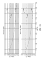
- FIG. 7A is diagrams of the first and second input signals of the capacitance to voltage amplifier 100 described with reference to FIG. 1 under common mode leakage.
- the leakage current is 0 A
- the voltage levels of the first input signal and the second input signal (represented by lines 702 a , 702 b ) is not affected as observed by lines 702 a , 702 b , which are flat.
- the leakage current 1 nano Amperes (nA)
- the voltages of the first input signal and the second input signal represented by lines 706 a , 706 b
- the voltages of the first input signal and the second input signal continue decreasing.
- the voltages of the first input signal and the second input signal (represented by lines 704 a , 704 b ) also decrease over time thereby degrading the first input bias value and the second input bias value.
- FIG. 7B is diagrams of the first and second input signals of the capacitance to voltage amplifier 200 described with reference to FIG. 4 under common mode leakage.
- the voltage of the first input signal (represented by line 712 a for a current level of 0 A, line 714 a for a current level between 0 A and 1 nA and line 716 a for a current level of 1 nA) is not affected.
- the voltage of the second input signal (represented by line 712 b for a leakage current of 0 A, line 714 b for a leakage current between 0 A and 1 nA and line 716 b for a leakage current of 1 nA) is also not affected. That is due to the fact that the leakage currents are compensated by the feedback loops 215 a , 215 b.
- FIG. 8A is diagrams of the first and second output signals of the capacitance to voltage amplifier 100 described with reference to FIG. 1 under differential mode leakage.
- the leakage current is 100 pico Ampere (pA)
- the voltages of the first output signal and the second output signal (represented by lines 730 a , 730 b ) diverge from 0.9V.
- the leakage current in differential mode is below 100 pA
- the voltages of the first output signal and the second output signal represented by four overlapping lines 722 - 728 a , 728 b ) is not affected.
- FIG. 8B is diagrams of the first and second output signals of the capacitance to voltage amplifier 200 described with reference to FIG. 4 under differential mode leakage.
- Lines 740 a , 740 b respectively represent the voltages of the first and second output signals of the capacitance to voltage amplifier 200 when the differential mode current leakage is 100 pA.
- the voltages initially diverge from a desired value of 0.9V.
- the feedback loops 215 a , 215 b compensate for the leakage current, the voltage converges to 0.9V over time.
- lines 732 - 738 a , 738 b show the voltages of the first and second output signals when the differential leakage current is varied from 0 A to a current below 100 pA.
- the feedback loops 215 a , 215 b compensate for the leakage current and over time the effect of the feedback loops 215 a , 215 b can be seen in FIG. 8B as the voltages of the first and second output signals converge over time to 0.9V.
Landscapes
- Engineering & Computer Science (AREA)
- Power Engineering (AREA)
- Amplifiers (AREA)
Abstract
Description
-
- i1=i1, i2=i2
icm=(i1+i2)/2, id=(i1−i2)
i1=icm+id/2, i2=icm−id/2
- i1=i1, i2=i2
and the second variable capacitor may vary according to
where C0 is a constant capacitor, Ω is an angular velocity associated with the first variable capacitor and the second variable capacitor and ωd is a drive oscillation frequency. The first operational amplifier may be configured to output a first voltage signal to compensate for a first current leakage at the first input terminal and the second operational amplifier may be configured to output a second voltage signal to compensate for a second current leakage at the second input terminal. The differential amplifier may be configured to receive a first input signal at the first input terminal and a second input signal at the second input terminal and output a first output signal at the first output terminal and a second output signal at the second output terminal. A difference between a voltage of the second output signal and a voltage of the first output signal may be proportional to a difference between a voltage of the first input signal and a voltage of the second input signal. The first low-pass filter may be configured to receive the first output signal and output a first filtered signal that is a direct current (DC) component of the first output signal. The first operational amplifier may be configured to receive the first input signal at the inverting input and the first filtered signal at the non-inverting input and output a first compensation signal that compensates for a first current leakage in the first input signal. The second low-pass filter may be configured to receive the second output signal and output a second filtered signal that may be a direct current (DC) component of the second output signal. The second operational amplifier may be configured to receive the second input signal at the inverting input and the second filtered signal at the non-inverting input and output a second compensation signal that compensates for a second current leakage affecting the second input signal.
where C0 is a constant capacitance, Ω is an angular velocity (for example, of a gyroscope driving the stage 110), ωd is a modulating frequency (for example, the driving frequency of the gyroscope) and sin is the sine operator. The second
where RF is the resistance of the
Claims (20)
Priority Applications (1)
| Application Number | Priority Date | Filing Date | Title |
|---|---|---|---|
| US14/947,908 US9455668B1 (en) | 2015-11-20 | 2015-11-20 | Capacitance to voltage converter with a leakage compensation loop |
Applications Claiming Priority (1)
| Application Number | Priority Date | Filing Date | Title |
|---|---|---|---|
| US14/947,908 US9455668B1 (en) | 2015-11-20 | 2015-11-20 | Capacitance to voltage converter with a leakage compensation loop |
Publications (1)
| Publication Number | Publication Date |
|---|---|
| US9455668B1 true US9455668B1 (en) | 2016-09-27 |
Family
ID=56939695
Family Applications (1)
| Application Number | Title | Priority Date | Filing Date |
|---|---|---|---|
| US14/947,908 Active US9455668B1 (en) | 2015-11-20 | 2015-11-20 | Capacitance to voltage converter with a leakage compensation loop |
Country Status (1)
| Country | Link |
|---|---|
| US (1) | US9455668B1 (en) |
Cited By (4)
| Publication number | Priority date | Publication date | Assignee | Title |
|---|---|---|---|---|
| US10141964B1 (en) * | 2017-10-02 | 2018-11-27 | King Fahd University Of Petroleum And Minerals | Low-power channel select filter using transresistance amplifier for DVB-H receivers |
| KR20200011877A (en) * | 2018-07-25 | 2020-02-04 | 쟈인 에레쿠토로닉스 가부시키가이샤 | Voltage-controlled oscillator, pll circuit, and cdr device |
| CN111937284A (en) * | 2018-02-15 | 2020-11-13 | Tdk电子股份有限公司 | Compensation filter and method for initiating compensation filter |
| CN115942191A (en) * | 2021-10-04 | 2023-04-07 | 茂达电子股份有限公司 | MEMS thin film speaker device |
Citations (7)
| Publication number | Priority date | Publication date | Assignee | Title |
|---|---|---|---|---|
| US5334952A (en) * | 1993-03-29 | 1994-08-02 | Spectralink Corporation | Fast settling phase locked loop |
| US5990751A (en) * | 1997-10-16 | 1999-11-23 | Nikon Corporation | Method and apparatus for improving power transfer efficiency of an amplifier system |
| US20030174023A1 (en) * | 2002-03-12 | 2003-09-18 | Tokio Miyasita | Analog summing and differencing circuit, optical receiving circuit, optical transmitting circuit, automatic gain control amplifier, automatic frequency compensation amplifier, and limiting amplifier |
| US20080030184A1 (en) * | 2006-08-07 | 2008-02-07 | Denso Corporation | System for smoothing output voltage or power generator |
| US20080106330A1 (en) * | 2006-09-07 | 2008-05-08 | Takeshi Yoshida | Feedback amplifier circuit operable at low voltage by utilizing switched operational amplifier and chopper modulator |
| US20140065979A1 (en) | 2012-08-31 | 2014-03-06 | Broadcom Corporation | Dc offset cancellation |
| US20160091525A1 (en) * | 2014-09-30 | 2016-03-31 | Hitachi, Ltd. | Acceleration sensor |
-
2015
- 2015-11-20 US US14/947,908 patent/US9455668B1/en active Active
Patent Citations (7)
| Publication number | Priority date | Publication date | Assignee | Title |
|---|---|---|---|---|
| US5334952A (en) * | 1993-03-29 | 1994-08-02 | Spectralink Corporation | Fast settling phase locked loop |
| US5990751A (en) * | 1997-10-16 | 1999-11-23 | Nikon Corporation | Method and apparatus for improving power transfer efficiency of an amplifier system |
| US20030174023A1 (en) * | 2002-03-12 | 2003-09-18 | Tokio Miyasita | Analog summing and differencing circuit, optical receiving circuit, optical transmitting circuit, automatic gain control amplifier, automatic frequency compensation amplifier, and limiting amplifier |
| US20080030184A1 (en) * | 2006-08-07 | 2008-02-07 | Denso Corporation | System for smoothing output voltage or power generator |
| US20080106330A1 (en) * | 2006-09-07 | 2008-05-08 | Takeshi Yoshida | Feedback amplifier circuit operable at low voltage by utilizing switched operational amplifier and chopper modulator |
| US20140065979A1 (en) | 2012-08-31 | 2014-03-06 | Broadcom Corporation | Dc offset cancellation |
| US20160091525A1 (en) * | 2014-09-30 | 2016-03-31 | Hitachi, Ltd. | Acceleration sensor |
Cited By (4)
| Publication number | Priority date | Publication date | Assignee | Title |
|---|---|---|---|---|
| US10141964B1 (en) * | 2017-10-02 | 2018-11-27 | King Fahd University Of Petroleum And Minerals | Low-power channel select filter using transresistance amplifier for DVB-H receivers |
| CN111937284A (en) * | 2018-02-15 | 2020-11-13 | Tdk电子股份有限公司 | Compensation filter and method for initiating compensation filter |
| KR20200011877A (en) * | 2018-07-25 | 2020-02-04 | 쟈인 에레쿠토로닉스 가부시키가이샤 | Voltage-controlled oscillator, pll circuit, and cdr device |
| CN115942191A (en) * | 2021-10-04 | 2023-04-07 | 茂达电子股份有限公司 | MEMS thin film speaker device |
Similar Documents
| Publication | Publication Date | Title |
|---|---|---|
| US7616078B2 (en) | Device for controlling the frequency of resonance of an oscillating micro-electromechanical system | |
| EP2430751B1 (en) | Transimpedance amplifier with distributed control of feedback line | |
| US9455668B1 (en) | Capacitance to voltage converter with a leakage compensation loop | |
| KR100733439B1 (en) | A constant-voltage circuit | |
| CN105278602B (en) | system and method for linear voltage regulator | |
| US20130147548A1 (en) | Linear amplifier that perform level shift and method of level shifting | |
| US20120013351A1 (en) | Method for converting a sensor capacitance under parasitic capacitance conditions and a capacitance-to-voltage converter circuit | |
| JP4515241B2 (en) | Output amplifier circuit and sensor device using the same | |
| US6795752B1 (en) | Thermal convection accelerometer with closed-loop heater control | |
| US10797664B2 (en) | Apparatuses and methods for a chopper instrumentation amplifier | |
| CN113922776A (en) | C/V conversion circuit based on switch capacitor type common mode feedback charge amplifier | |
| EP4080761A1 (en) | Analog front-end circuit for bioelectric sensor | |
| US7061309B2 (en) | Transconductance-adjusting circuit | |
| CN105788559A (en) | Voltage stabilizing device | |
| CN103048922B (en) | Based on the simulation pi controller circuit of transconductance-capacitor structure | |
| JP2008009968A (en) | Voltage generating apparatus, current generating apparatus, and test apparatus | |
| US10126769B2 (en) | Class-D driven low-drop-output (LDO) regulator | |
| Saukoski et al. | Integrated readout and control electronics for a microelectromechanical angular velocity sensor | |
| US7812685B2 (en) | Automatic regulator of filter | |
| US8653858B2 (en) | Signal operating circuit | |
| US8878636B2 (en) | Techniques for developing a negative impedance | |
| JP5559733B2 (en) | Physical quantity sensor | |
| US20120268218A1 (en) | Vibration circuit | |
| JP2008205561A (en) | Source follower circuit and semiconductor device | |
| TWI650937B (en) | Drive circuit |
Legal Events
| Date | Code | Title | Description |
|---|---|---|---|
| AS | Assignment |
Owner name: STMICROELECTRONICS S.R.L., ITALY Free format text: ASSIGNMENT OF ASSIGNORS INTEREST;ASSIGNORS:GARBARINO, MARCO;DONADEL, ANDREA;REEL/FRAME:037130/0602 Effective date: 20151120 |
|
| STCF | Information on status: patent grant |
Free format text: PATENTED CASE |
|
| MAFP | Maintenance fee payment |
Free format text: PAYMENT OF MAINTENANCE FEE, 4TH YEAR, LARGE ENTITY (ORIGINAL EVENT CODE: M1551); ENTITY STATUS OF PATENT OWNER: LARGE ENTITY Year of fee payment: 4 |
|
| MAFP | Maintenance fee payment |
Free format text: PAYMENT OF MAINTENANCE FEE, 8TH YEAR, LARGE ENTITY (ORIGINAL EVENT CODE: M1552); ENTITY STATUS OF PATENT OWNER: LARGE ENTITY Year of fee payment: 8 |