US9449636B2 - Optical disc actuator and optical disc drive device - Google Patents
Optical disc actuator and optical disc drive device Download PDFInfo
- Publication number
- US9449636B2 US9449636B2 US14/507,830 US201414507830A US9449636B2 US 9449636 B2 US9449636 B2 US 9449636B2 US 201414507830 A US201414507830 A US 201414507830A US 9449636 B2 US9449636 B2 US 9449636B2
- Authority
- US
- United States
- Prior art keywords
- coil
- optical disc
- movable portion
- magnet
- coil patterns
- Prior art date
- Legal status (The legal status is an assumption and is not a legal conclusion. Google has not performed a legal analysis and makes no representation as to the accuracy of the status listed.)
- Expired - Fee Related
Links
Images


Classifications
-
- G—PHYSICS
- G11—INFORMATION STORAGE
- G11B—INFORMATION STORAGE BASED ON RELATIVE MOVEMENT BETWEEN RECORD CARRIER AND TRANSDUCER
- G11B7/00—Recording or reproducing by optical means, e.g. recording using a thermal beam of optical radiation by modifying optical properties or the physical structure, reproducing using an optical beam at lower power by sensing optical properties; Record carriers therefor
- G11B7/08—Disposition or mounting of heads or light sources relatively to record carriers
- G11B7/09—Disposition or mounting of heads or light sources relatively to record carriers with provision for moving the light beam or focus plane for the purpose of maintaining alignment of the light beam relative to the record carrier during transducing operation, e.g. to compensate for surface irregularities of the latter or for track following
- G11B7/0925—Electromechanical actuators for lens positioning
- G11B7/0935—Details of the moving parts
-
- G—PHYSICS
- G11—INFORMATION STORAGE
- G11B—INFORMATION STORAGE BASED ON RELATIVE MOVEMENT BETWEEN RECORD CARRIER AND TRANSDUCER
- G11B7/00—Recording or reproducing by optical means, e.g. recording using a thermal beam of optical radiation by modifying optical properties or the physical structure, reproducing using an optical beam at lower power by sensing optical properties; Record carriers therefor
- G11B7/08—Disposition or mounting of heads or light sources relatively to record carriers
- G11B7/09—Disposition or mounting of heads or light sources relatively to record carriers with provision for moving the light beam or focus plane for the purpose of maintaining alignment of the light beam relative to the record carrier during transducing operation, e.g. to compensate for surface irregularities of the latter or for track following
- G11B7/0925—Electromechanical actuators for lens positioning
- G11B7/093—Electromechanical actuators for lens positioning for focusing and tracking
-
- G—PHYSICS
- G11—INFORMATION STORAGE
- G11B—INFORMATION STORAGE BASED ON RELATIVE MOVEMENT BETWEEN RECORD CARRIER AND TRANSDUCER
- G11B7/00—Recording or reproducing by optical means, e.g. recording using a thermal beam of optical radiation by modifying optical properties or the physical structure, reproducing using an optical beam at lower power by sensing optical properties; Record carriers therefor
- G11B7/08—Disposition or mounting of heads or light sources relatively to record carriers
- G11B7/09—Disposition or mounting of heads or light sources relatively to record carriers with provision for moving the light beam or focus plane for the purpose of maintaining alignment of the light beam relative to the record carrier during transducing operation, e.g. to compensate for surface irregularities of the latter or for track following
- G11B7/0925—Electromechanical actuators for lens positioning
- G11B7/0933—Details of stationary parts
Definitions
- the present invention relates to a printed coil substrate for an optical disc actuator, an optical disc pickup, and an optical disc drive device.
- An optical disc pickup is equipped on an optical disc drive device, and an optical disc actuator is equipped on the optical disc pickup.
- the optical disc actuator in order to drive a movable portion having an objective lens relatively to a fixed portion, a magnet is equipped on one of the movable portion and the fixed portion, and an electromagnetic coil is equipped on the other. The electromagnetic coil is attracted and repelled by the magnet by magnetic flux generated when a current is made to flow, and the movable portion is driven relatively to the fixed portion.
- the fixed portion itself is linearly driven in a radial direction of an optical disc.
- a surface of the optical disc can be scanned because the fixed portion is linearly driven in the radial direction while the optical disc is rotary driven.
- the electromagnetic coil can be formed of a wire coil or a printed coil substrate, which is made by forming a coil pattern on a flexible substrate.
- the movable portion In the optical disc actuator, the movable portion is held at a neutral position in terms of design so that magnetic force from the magnet (permanent magnet) can be obtained the most.
- the movable portion When the movable portion is shifted (moved) in a focal direction or a tracking direction from the neutral position, an effective part of the coil, which generates a driving force, is also shifted. Therefore, sensitivity is deteriorated and recording and reproducing performance are negatively affected.
- the sensitivity is a general term of accuracy for moving the movable portion to an appropriate position based on attraction force and repulsive force generated when an electric current is applied to the coil of the movable portion in the magnetic flux of the magnet.
- Patent documents 1 to 5 are known.
- pattern width of a coil pattern formed in a layer near a magnet is made narrower than the pattern width of the coil pattern formed in a layer far from the magnet.
- Patent document 3 a plurality of printed substrates on which a focusing coil and a tracking coil are formed as a circuit pattern are laminated so that the focusing coil and the tracking coil are not overlapped in a thickness direction of the printed substrates.
- each of coil elements is composed of a circuit pattern formed on a printed substrate, shapes of the circuit pattern are different in each phase, and a length of an effective conductive part contributing to a driving force of the coil is set shorter in an effective coil close to the magnet than others.
- Patent document 1 Japanese Patent Application Laid-Open No. 2005-166219
- Patent document 2 Japanese Patent Application Laid-Open No. 2007-080305
- Patent document 3 Japanese Patent Application Laid-Open No. H07-093778
- Patent document 4 Japanese Patent Application Laid-Open No. H07-210884
- Patent document 5 Japanese Patent Application Laid-Open No. 2006-040415
- Patent document 1 although the influence of the land part can be reduced, sensitivity is largely changed when shifting in a focusing direction and in a tracking direction.
- Patent documents 2 and 4 although the difference caused by the change of distance from the magnet in a plurality of the printed coil substrates can be solved, the sensitivity is largely changed.
- the present invention provides a printed coil substrate for an optical disc actuator, an optical disc pickup, and an optical disc drive device so that the sensitivity will change as little as possible when shifting in a focal direction and a tracking direction.
- One aspect of the present invention provides a printed coil substrate for an optical disc actuator so as to drive a movable portion of the optical disc actuator relatively to a fixed portion, wherein the printed coil substrate is formed by a plurality of laminated substrate layers, coil patterns are formed on predetermined portions of each of the substrate layers, the coil patterns of the substrate layers having an approximately same shape are connected with each other between the coil patterns laminated at a corresponding position so that coils are formed at each of the predetermined portions, center locations in shape of the coil patterns, which are formed on the substrate layers to form the coils, are displaced between neighboring substrate layers, and the center locations are displaced by a predetermined distance toward a direction of driving the movable portion driven by each of the coils.
- the coil patterns are formed on predetermined portions of each of the substrate layers and the coil patterns having an approximately same shape are connected with each other between the coil patterns laminated at a corresponding position while the substrate layers are laminated, the coils are formed at each of the predetermined portions.
- the center locations in shape of the coil patterns, which are formed on the substrate layers to form the coils are matched with a center of the corresponding magnet.
- the center locations in shape of the coil patterns, which are formed on the substrate layers to form the coils are displaced between neighboring substrate layers, and the center locations are displaced by a predetermined distance toward a direction of driving the movable portion driven by each of the coils.
- a width of magnetic flux formed by two substrate layers becomes wide in a so-called shift direction.
- optical disc pickup or the optical disc drive device having the optical disc actuator of such configuration the same operations and effects are achieved.
- FIG. 1 is a schematic block diagram of an optical disc drive device.
- FIG. 2 is a perspective view of an optical disc pickup.
- FIG. 3 is a perspective view of a movable portion.
- FIG. 4 is a schematic diagram showing a laminated state of printed coil substrates.
- FIG. 5 is a schematic diagram showing an overlapped state of coil patterns.
- FIG. 6 is a schematic diagram showing magnetic flux of a magnet and a position of the coil patterns.
- FIG. 7 is a diagram showing an amount of change of sensitivity before and after countermeasure is applied to a focus coil.
- FIG. 8 is a diagram showing an amount of change of sensitivity before and after countermeasure is applied to a tracking coil.
- FIG. 9 is a schematic diagram showing an overlapped state of coil patterns when a substrate layer includes four layers.
- FIG. 10 is a schematic diagram showing a variation example of an overlapped state of coil patterns when a substrate layer includes four layers.
- FIG. 11 is a diagram showing a variation example of the coil patterns.
- FIG. 12 is a diagram showing the coil patterns with an enlarged view.
- FIG. 13 is a diagram showing a variation example of a distance of displacing center locations.
- FIG. 14 is a diagram showing a distance of displacing center locations.
- FIG. 15 is a diagram showing a variation example of a coil width.
- FIG. 1 is a schematic block diagram of an optical disc drive device.
- FIG. 2 is a perspective view of an optical disc pickup including a fixed portion.
- FIG. 3 is a perspective view of a movable portion.
- An optical disc pickup 11 is equipped on an optical disc drive device 10 .
- An optical disc actuator which will be explained later, is equipped on the optical disc pickup 11 .
- a magnet 13 a is equipped on one of the movable portion 12 and the fixed portion 13 , and an electromagnetic coil 12 a is equipped on the other.
- the electromagnetic coil 12 a is attracted and repelled by the magnet 13 a by magnetic flux generated when a current is made to flow, and the movable portion 12 is driven relatively to the fixed portion 13 .
- the fixed portion 13 itself is linearly driven in a radial direction of a not illustrated optical disc by a stepping motor 14 a .
- a surface of the optical disc can be scanned because the fixed portion 13 is linearly driven in the radial direction (capable of moving linearly) while the optical disc is rotary driven (capable of moving rotatively) by a DC motor 14 b .
- a control portion 15 is equipped so as to control the driving of the stepping motor 14 a and the DC motor 14 b and control recording and reproducing executed by the optical disc pickup 11 .
- the optical disc pickup 11 has the movable portion 12 and the fixed portion 13 , and the movable portion 12 is floatingly supported on the fixed portion 13 by wires 12 c , which are equipped three on the left and three on the right.
- the “floatingly supported” means, in general, the movable portion 12 is supported by the fixed portion 13 via an elastic body. Since the elastic body is deformed, a relative positional relation between the fixed portion 13 and the movable portion 12 can be changed by a minute distance. Therefore, the wires 12 c , three on the left and three on the right, are corresponding to the elastic body.
- the movable portion 12 can be moved by a minute distance at least in a focal direction (Z-axis direction), which is a direction of approaching to and separating from a surface of the optical disc, and in a tracking direction (X-axis direction), which is a radial direction of the optical disc.
- Z-axis direction a focal direction
- X-axis direction a tracking direction of the optical disc.
- the coil patterns have a focus coil 22 b to drive the movable portion 12 in the Z-axis direction and a tracking coil 22 a to drive the movable portion 12 in an XY plane (X-axis direction).
- An objective lens 12 b which is composed of a first objective lens 12 b 1 and a second objective lens 12 b 2 , is fixed on the movable portion 12 .
- the first objective lens 12 b 1 and the second objective lens 12 b 2 are corresponding respectively to Blu-ray disc and other optical discs.
- the objective lens 12 b is held by a lens holder 18 , and a lens protector 18 a is equipped on the lens holder 18 projecting between the first objective lens 12 b 1 and the second objective lens 12 b 2 so that the objective lenses are not interfere with the surface of the optical disc.
- the wires 12 c also have a function of supplying the power to the electromagnetic coil 12 a .
- Intermediate substrates 19 are provided on both an inner side and an outer side of the radial direction of the movable portion 12 so as to electrically connect the wires 12 c with the electromagnetic coil 12 a and to support the movable portion 12 itself.
- the magnet 13 a is a so-called bipolar magnet and the magnet 13 a is supported by a yoke base 13 b.
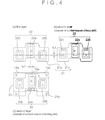
- FIG. 4 is a schematic diagram showing a laminated state of the printed coil substrates.
- the electromagnetic coil 12 a is composed of a printed coil substrate 20 .
- the printed coil substrate 20 is formed by a plurality of laminated substrate layers 21 , which are made by a flexible substrate. Each of the substrate layers 21 is formed by sandwiching both ends of a coil pattern 22 of a spiral shape, which is arranged at a predetermined position, between insulation boards.
- a plurality of the substrate layers 21 is defined as a substrate layer 21 a for the first layer and a substrate layer 21 b for the second layer, shapes of the coil patterns 22 of the substrate layer 21 a and the substrate layer 21 b are approximately same.
- positions of through holes, which are used for electrically connecting the coil patterns 22 , 22 to form the coil while two of the substrate layers 21 a , 21 b are laminated, are different.
- the coil pattern 22 is composed of a tracking coil 22 a arranged at the center, and focus coils 22 b , 22 b arranged at both sides of the tracking coil 22 a.
- the coil patterns which are overlapped at a corresponding position when laminated, are approximately same shape, center locations in shape of the tracking coil 22 a and the focus coils 22 b , 22 b are not matched between the neighboring substrate layers 21 a , 21 b.
- the center locations are specified to be displaced by a predetermined distance in a direction of driving the movable portion 12 by each of the coils.
- the centers of the tracking coil 22 a are displaced by a coil width (tc 1 ) in the width direction between the substrate layer 21 a of the first layer and the substrate layer 21 b of the second layer.
- the centers of the focus coil 22 b are displaced by a coil width (fc 1 ) in the vertical direction between the substrate layer 21 a of the first layer and the substrate layer 21 b of the second layer.
- the width direction is a tracking direction, which is a direction of driving the movable portion 12 by the tracking coil 22 a .
- the vertical direction is a focal direction which is a direction of driving the movable portion 12 by the focus coil 22 b.
- the shape center of the focus coil 22 b of the substrate layer 21 a of the first layer is offset upward from a position where magnetic force of the opposing magnet 13 a is strong, for example, the shape center of the focus coil 22 b of the substrate layer 21 b of the second layer is offset downward, contrary to the first layer.
- the shape center of the focus coil 22 b of the substrate layer 21 a of the first layer is offset downward from the position where magnetic force of the opposite magnet 13 a is strong, the shape center of the focus coil 22 b of the substrate layer 21 b of the second layer is offset upward, contrary to the first layer.
- Offset amounts of the first layer and the second layer are decided in the design stage so that difference of magnetic flux density distribution between the layers and change of the sensitivity within the necessary shift range become the least. Thus, change of the sensitivity during a focus shift can be suppressed.
- the center locations can be arranged in the same way although the direction of the offset is horizontal.
- the shape center of the tracking coil 22 a of the substrate layer 21 a of the first layer is offset leftward from the position where magnetic force of the magnet 13 a is strong, for example, the shape center of the tracking coil 22 a of the substrate layer 21 b of the second layer is offset rightward, contrary to the first layer.
- the shape center of the tracking coil 22 a of the substrate layer 21 a of the first layer is offset rightward from the position where magnetic force of the magnet 13 a is strong, the tracking coil 22 a of the substrate layer 21 b of the second layer is offset leftward, contrary to the first layer.
- the predetermined distance to be displaced is approximately corresponding to the coil width in this example.
- the coil width is 0.1 mm in the tracking coil 22 a and 0.5 mm in the focus coil 22 b . Therefore, the coil pattern of the focus coil 22 b is displaced longer distance than the coil pattern of the tracking coil 22 a.
- a distance of driving the movable portion 12 by the focus coil 22 b is longer than a distance of driving the movable portion 12 by the tracking coil 22 a . Therefore, the distance to be displaced varies according to the direction of driving the movable portion 12 by each of the coils, and the distance to be displaced is longer in a direction toward which a drive distance of the movable portion 12 is longer than a direction toward which the drive distance is shorter.
- FIG. 5 is a schematic diagram showing an overlapped state of coil patterns.
- the figure shows a state that two focus coils 22 b , one is for the substrate layer 21 a of the first layer and the other is for the substrate layer 21 b , are laminated while being relatively displaced vertically.
- the figure shows the focus coils 22 b , the tracking coils 22 a are laminated while being relatively displaced horizontally in the same way.
- FIG. 6 is a schematic diagram showing magnetic flux of the magnet and a position of the coil patterns. Note that the magnet 13 a is roughly illustrated.
- magnetic flux density of the magnet 13 a reached to the substrate layer 21 a of the first layer is not same as magnetic flux density of the magnet 13 a reached to the substrate layer 21 b of the second layer. This is because the magnetic flux is stronger at the nearer side of the magnet 13 a and weaker at the farther side.
- the center locations in shape of the coil pattern are displaced between the substrate layer 21 a of the first layer and the substrate layer 21 b of the second layer. If the center locations are displaced, when the movable portion 12 is driven along the tracking direction or the focal direction, the magnetic flux density of the magnet 13 a does not suddenly decrease by the extent of increase of the width of the coil pattern.
- the coil pattern of the first layer is moved in a direction of leaving from the position where magnetic force of the magnet 13 a is strong
- the coil pattern of the second layer is simultaneously moved into the position where magnetic force of the magnet 13 a is strong. Therefore, the change of the sensitivity can be relatively compensated. Of course, the reverse also occurs.
- FIG. 7 is a diagram showing an amount of the change of the sensitivity before and after countermeasure is applied to the focus coil.
- FIG. 8 is a diagram showing an amount of the change of the sensitivity before and after countermeasure is applied to the tracking coil.
- the amount of change of sensitivity is different more than 1.0 dB at a position where the amount of the focus shift is about 0.4 mm.
- the amount of tracking shift almost same result is obtained.
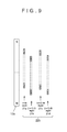
- FIG. 9 is a schematic diagram showing an overlapped state of the coil patterns when the substrate layer includes four layers.
- a direction of displacing the focus coil 22 b and the tracking coil 22 a is along a direction of driving the movable portion 12 , and is alternately changed between the neighboring layers.
- the substrate layers 21 include more than 3 layers and are formed by n-th layer (n: an integral equal to or more than 1), (n+1)-th layer, (n+2)-th layer, (n+3)-th layer - - - - , the direction (offset direction) of the coil patterns of the substrate layer 21 are same between n-th layer and (n+2)-th layer and different between n-th layer and (n+1)-th layer.
- the direction of displacing fluctuation of the magnetic flux is reduced and the magnetic flux can be generated more evenly. Consequently, the amount of change of sensitivity can be more flat.
- the offset directions are same between n-th layer and (n+2)-th layer.
- An offset amount is decided in the design stage considering the magnetic flux density of each layer so that the desired sensitivity is obtained in the same way as the case of two layers.
- FIG. 10 is a schematic diagram showing a variation example of an overlapped state of coil patterns when a substrate layer includes four layers.
- the direction of displacing is changed in every two layers. If a plurality of the coil patterns is laminated, performance as an electromagnetic coil is improved. Therefore, the performance as an electromagnetic coil can be improved by laminating the layers at the same position while the centers are matched, and at the same time, the amount of change of sensitivity can be flat by laminating a pair of the layers in which the centers are not matched.
- FIG. 11 is a diagram showing a variation example of the coil patterns.
- FIG. 12 is a diagram showing the coil patterns with an enlarged view.
- the coil patterns of this example is formed to be an approximately rectangular shape, the coil widths are almost same in three sides, and the coil width of the other side is specified to be wide portion (wide side).
- the wide portion is formed in a direction toward which the center locations of the coil patterns are displaced from the center of the magnet.
- the coil widths of the coil patterns are wide at a predetermined direction in the whole circumference, and the wide portion is formed in a direction toward which the center locations of the coil patterns are displaced from the center of the magnet
- the wide portion (wide side) is formed at a left side of the tracking coil 22 a in the substrate layer 21 a of the first layer, and the wide portion is formed at a right side of the tracking coil 22 a in the substrate layer 21 b of the second layer.
- the tracking coil 22 a is displaced to the left side in the substrate layer 21 a of the first layer, and the tracking coil 22 a is displaced to the right side in the substrate layer 21 b of the second layer.
- the above explanation is also applied to the focus coil 22 b .
- the wide portion is formed at a lower side of the focus coil 22 b in the substrate layer 21 a of the first layer, and the wide portion is formed at an upper side of the focus coil 22 b in the substrate layer 21 b of the second layer.
- the focus coil 22 b is displaced to the lower side in the substrate layer 21 a of the first layer, and the focus coil 22 b is displaced to the upper side in the substrate layer 21 b of the second layer.
- the coil width of the wide portion is 2 W, while the coil widths are W at other portions.
- the wide portion is arranged at a side of the direction of displacing a center location CC of the coil pattern from a center location MC of the magnet 13 a.
- the product can be designed enabling to prevent the sensitivity from being deteriorated against the shift by changing the coil width of the first layer and the second layer taking advantage of the printed coil, in addition to the offset of the center locations in shape of each layer.
- FIG. 13 and FIG. 14 are diagrams showing a variation example of a distance of displacing the center locations.
- the shape center of the coil pattern formed on the substrate layer 21 a of the first layer, which is nearer to the magnet 13 a , is CC 1 .
- a distance between CC 2 and MC, which is the center of the magnet 13 a is LC 2 .
- the following relation is satisfied. LC1 ⁇ LC2
- the distance between the center location in shape of the coil patterns and the center of the magnet becomes longer as substrate layer 21 is more distant from the magnet.
- the magnetic flux generated by the magnet 13 a varies in density according to the distance to each of the substrate layers 21 a , 21 b . Therefore, the sensitivity is influenced by the change of the density. In addition, if the density is low, it also means that magnetic flux is widely distributed. Considering the above, as an example to flatten the amount of change of sensitivity, the distance from the center of the magnet is specified to be longer at the farther side where the magnetic flux should be widely distributed.
- the relation is LC 1 ⁇ LC 2 in the example of FIG. 13 and FIG. 14 , the relation is not limited to this example.
- FIG. 15 is a diagram showing a variation example of the coil width.
- the coil width of the substrate layer 21 a of the first layer is narrower than the coil width of the substrate layer 21 a of the second layer.
- the coil width is wider in the substrate layer 21 a of the second layer.
- the coil width of the coil pattern is wider at nearer side to the magnet 13 a than the farther side.
- the difference of the coil width explained above is specified because distribution of the magnetic flux varies according to the distance from the magnet 13 a .
- the amount of change of sensitivity is flattened by widening the coil width at the farther side where the magnetic flux should be widely distributed.
Landscapes
- Optical Recording Or Reproduction (AREA)
- Optical Head (AREA)
Abstract
Description
LC1<LC2
-
- Mutually substitutable members, configurations, etc. disclosed in the embodiment can be used with their combination altered appropriately.
- Although not disclosed in the embodiment, members, configurations, etc. that belong to the known technology and can be substituted with the members, the configurations, etc. disclosed in the embodiment can be appropriately substituted or are used by altering their combination.
- Although not disclosed in the embodiment, members, configurations, etc. that those skilled in the art can consider as substitutions of the members, the configurations, etc. disclosed in the embodiment are substituted with the above mentioned appropriately or are used by altering its combination.
Claims (11)
Applications Claiming Priority (2)
| Application Number | Priority Date | Filing Date | Title |
|---|---|---|---|
| JP2013226648A JP6191399B2 (en) | 2013-10-31 | 2013-10-31 | Printed coil substrate for optical disk actuator, optical disk pickup, optical disk drive device |
| JP2013-226648 | 2013-10-31 |
Publications (2)
| Publication Number | Publication Date |
|---|---|
| US20150121403A1 US20150121403A1 (en) | 2015-04-30 |
| US9449636B2 true US9449636B2 (en) | 2016-09-20 |
Family
ID=52997013
Family Applications (1)
| Application Number | Title | Priority Date | Filing Date |
|---|---|---|---|
| US14/507,830 Expired - Fee Related US9449636B2 (en) | 2013-10-31 | 2014-10-07 | Optical disc actuator and optical disc drive device |
Country Status (2)
| Country | Link |
|---|---|
| US (1) | US9449636B2 (en) |
| JP (1) | JP6191399B2 (en) |
Citations (6)
| Publication number | Priority date | Publication date | Assignee | Title |
|---|---|---|---|---|
| JPH0793778A (en) | 1993-09-21 | 1995-04-07 | Sony Corp | Biaxial actuator for optical pickup device |
| JPH07210884A (en) | 1994-01-21 | 1995-08-11 | Sony Corp | Biaxial actuator for optical pickup device |
| US20040252596A1 (en) * | 2003-06-13 | 2004-12-16 | Cho Won-Ik | Molded coil device for actuator of disc drive |
| JP2005166219A (en) | 2003-12-05 | 2005-06-23 | Ricoh Co Ltd | Printed coil substrate, objective lens driving device, optical pickup and optical disk device |
| JP2006040415A (en) | 2004-07-27 | 2006-02-09 | Ricoh Co Ltd | Objective lens driving device, optical pickup, and optical disk drive |
| JP2007080305A (en) | 2005-09-09 | 2007-03-29 | Ricoh Co Ltd | Objective lens drive, optical pickup, optical disk drive |
Family Cites Families (1)
| Publication number | Priority date | Publication date | Assignee | Title |
|---|---|---|---|---|
| JPS61150139A (en) * | 1984-12-25 | 1986-07-08 | Toshiba Corp | Objective lens driving device of optical information processor |
-
2013
- 2013-10-31 JP JP2013226648A patent/JP6191399B2/en not_active Expired - Fee Related
-
2014
- 2014-10-07 US US14/507,830 patent/US9449636B2/en not_active Expired - Fee Related
Patent Citations (6)
| Publication number | Priority date | Publication date | Assignee | Title |
|---|---|---|---|---|
| JPH0793778A (en) | 1993-09-21 | 1995-04-07 | Sony Corp | Biaxial actuator for optical pickup device |
| JPH07210884A (en) | 1994-01-21 | 1995-08-11 | Sony Corp | Biaxial actuator for optical pickup device |
| US20040252596A1 (en) * | 2003-06-13 | 2004-12-16 | Cho Won-Ik | Molded coil device for actuator of disc drive |
| JP2005166219A (en) | 2003-12-05 | 2005-06-23 | Ricoh Co Ltd | Printed coil substrate, objective lens driving device, optical pickup and optical disk device |
| JP2006040415A (en) | 2004-07-27 | 2006-02-09 | Ricoh Co Ltd | Objective lens driving device, optical pickup, and optical disk drive |
| JP2007080305A (en) | 2005-09-09 | 2007-03-29 | Ricoh Co Ltd | Objective lens drive, optical pickup, optical disk drive |
Also Published As
| Publication number | Publication date |
|---|---|
| JP2015088206A (en) | 2015-05-07 |
| JP6191399B2 (en) | 2017-09-06 |
| US20150121403A1 (en) | 2015-04-30 |
Similar Documents
| Publication | Publication Date | Title |
|---|---|---|
| KR101494823B1 (en) | Camera module | |
| US10423005B2 (en) | Electromagnetic driving module and lens driving device using the same | |
| US5949590A (en) | Actuator for optical pickup apparatus | |
| JP2017068267A (en) | Electromagnetic drive module and lens driving device using the same | |
| US12449715B2 (en) | Shape memory alloy actuator | |
| EP1486992B1 (en) | Actuator with molded coil device for disc drive | |
| US9449636B2 (en) | Optical disc actuator and optical disc drive device | |
| JP2008146819A (en) | Printed circuit board for an optical pickup with interleaved tilt and focus windings printed thereon | |
| CN110959250B (en) | Actuator | |
| CN213213591U (en) | Optical element driving mechanism | |
| JP4751678B2 (en) | Objective lens drive, optical pickup, optical disk drive | |
| US7663984B2 (en) | Optical pickup actuator for driving an objective lens | |
| US8004937B2 (en) | Optical pickup and optical disk apparatus | |
| US20250271729A1 (en) | Lens drive device and camera module | |
| JP2009158071A (en) | Actuator and optical pickup device including actuator | |
| KR100791837B1 (en) | Hard disk drive | |
| CN111077631A (en) | Lens driving device and base | |
| EP1914763B1 (en) | Printed circuit board having printed coils thereon | |
| JP4484615B2 (en) | Objective lens driving device, optical pickup, and optical disk drive | |
| JP5389862B2 (en) | Objective lens driving device and optical pickup using the same | |
| KR101275318B1 (en) | lens actuating unit of optical pickup and disc drive adopting the actuator | |
| JP2010233277A (en) | Electromagnetic transducer | |
| JP2005310237A (en) | Objective lens drive | |
| JP2007164879A (en) | Objective lens driving device | |
| JP2007200551A (en) | Lens driving device |
Legal Events
| Date | Code | Title | Description |
|---|---|---|---|
| AS | Assignment |
Owner name: FUNAI ELECTRIC CO., LTD., JAPAN Free format text: ASSIGNMENT OF ASSIGNORS INTEREST;ASSIGNOR:HOSODA, RYOZO;REEL/FRAME:033897/0013 Effective date: 20141002 |
|
| STCF | Information on status: patent grant |
Free format text: PATENTED CASE |
|
| MAFP | Maintenance fee payment |
Free format text: PAYMENT OF MAINTENANCE FEE, 4TH YEAR, LARGE ENTITY (ORIGINAL EVENT CODE: M1551); ENTITY STATUS OF PATENT OWNER: LARGE ENTITY Year of fee payment: 4 |
|
| FEPP | Fee payment procedure |
Free format text: MAINTENANCE FEE REMINDER MAILED (ORIGINAL EVENT CODE: REM.); ENTITY STATUS OF PATENT OWNER: LARGE ENTITY |
|
| LAPS | Lapse for failure to pay maintenance fees |
Free format text: PATENT EXPIRED FOR FAILURE TO PAY MAINTENANCE FEES (ORIGINAL EVENT CODE: EXP.); ENTITY STATUS OF PATENT OWNER: LARGE ENTITY |
|
| STCH | Information on status: patent discontinuation |
Free format text: PATENT EXPIRED DUE TO NONPAYMENT OF MAINTENANCE FEES UNDER 37 CFR 1.362 |
|
| STCH | Information on status: patent discontinuation |
Free format text: PATENT EXPIRED DUE TO NONPAYMENT OF MAINTENANCE FEES UNDER 37 CFR 1.362 |
|
| FP | Lapsed due to failure to pay maintenance fee |
Effective date: 20240920 |