US9448472B2 - Optical pattern transfer mask and method of fabricating the same - Google Patents
Optical pattern transfer mask and method of fabricating the same Download PDFInfo
- Publication number
- US9448472B2 US9448472B2 US14/640,512 US201514640512A US9448472B2 US 9448472 B2 US9448472 B2 US 9448472B2 US 201514640512 A US201514640512 A US 201514640512A US 9448472 B2 US9448472 B2 US 9448472B2
- Authority
- US
- United States
- Prior art keywords
- layer
- light
- polymer
- diels
- alder
- Prior art date
- Legal status (The legal status is an assumption and is not a legal conclusion. Google has not performed a legal analysis and makes no representation as to the accuracy of the status listed.)
- Expired - Fee Related, expires
Links
Images


Classifications
-
- H—ELECTRICITY
- H10—SEMICONDUCTOR DEVICES; ELECTRIC SOLID-STATE DEVICES NOT OTHERWISE PROVIDED FOR
- H10K—ORGANIC ELECTRIC SOLID-STATE DEVICES
- H10K71/00—Manufacture or treatment specially adapted for the organic devices covered by this subclass
-
- G—PHYSICS
- G03—PHOTOGRAPHY; CINEMATOGRAPHY; ANALOGOUS TECHNIQUES USING WAVES OTHER THAN OPTICAL WAVES; ELECTROGRAPHY; HOLOGRAPHY
- G03F—PHOTOMECHANICAL PRODUCTION OF TEXTURED OR PATTERNED SURFACES, e.g. FOR PRINTING, FOR PROCESSING OF SEMICONDUCTOR DEVICES; MATERIALS THEREFOR; ORIGINALS THEREFOR; APPARATUS SPECIALLY ADAPTED THEREFOR
- G03F7/00—Photomechanical, e.g. photolithographic, production of textured or patterned surfaces, e.g. printing surfaces; Materials therefor, e.g. comprising photoresists; Apparatus specially adapted therefor
- G03F7/004—Photosensitive materials
- G03F7/039—Macromolecular compounds which are photodegradable, e.g. positive electron resists
-
- B—PERFORMING OPERATIONS; TRANSPORTING
- B41—PRINTING; LINING MACHINES; TYPEWRITERS; STAMPS
- B41M—PRINTING, DUPLICATING, MARKING, OR COPYING PROCESSES; COLOUR PRINTING
- B41M5/00—Duplicating or marking methods; Sheet materials for use therein
- B41M5/26—Thermography ; Marking by high energetic means, e.g. laser otherwise than by burning, and characterised by the material used
- B41M5/40—Thermography ; Marking by high energetic means, e.g. laser otherwise than by burning, and characterised by the material used characterised by the base backcoat, intermediate, or covering layers, e.g. for thermal transfer dye-donor or dye-receiver sheets; Heat, radiation filtering or absorbing means or layers; combined with other image registration layers or compositions; Special originals for reproduction by thermography
- B41M5/42—Intermediate, backcoat, or covering layers
- B41M5/44—Intermediate, backcoat, or covering layers characterised by the macromolecular compounds
- B41M5/443—Silicon-containing polymers, e.g. silicones, siloxanes
-
- G—PHYSICS
- G03—PHOTOGRAPHY; CINEMATOGRAPHY; ANALOGOUS TECHNIQUES USING WAVES OTHER THAN OPTICAL WAVES; ELECTROGRAPHY; HOLOGRAPHY
- G03F—PHOTOMECHANICAL PRODUCTION OF TEXTURED OR PATTERNED SURFACES, e.g. FOR PRINTING, FOR PROCESSING OF SEMICONDUCTOR DEVICES; MATERIALS THEREFOR; ORIGINALS THEREFOR; APPARATUS SPECIALLY ADAPTED THEREFOR
- G03F1/00—Originals for photomechanical production of textured or patterned surfaces, e.g., masks, photo-masks, reticles; Mask blanks or pellicles therefor; Containers specially adapted therefor; Preparation thereof
- G03F1/38—Masks having auxiliary features, e.g. special coatings or marks for alignment or testing; Preparation thereof
-
- G—PHYSICS
- G03—PHOTOGRAPHY; CINEMATOGRAPHY; ANALOGOUS TECHNIQUES USING WAVES OTHER THAN OPTICAL WAVES; ELECTROGRAPHY; HOLOGRAPHY
- G03F—PHOTOMECHANICAL PRODUCTION OF TEXTURED OR PATTERNED SURFACES, e.g. FOR PRINTING, FOR PROCESSING OF SEMICONDUCTOR DEVICES; MATERIALS THEREFOR; ORIGINALS THEREFOR; APPARATUS SPECIALLY ADAPTED THEREFOR
- G03F7/00—Photomechanical, e.g. photolithographic, production of textured or patterned surfaces, e.g. printing surfaces; Materials therefor, e.g. comprising photoresists; Apparatus specially adapted therefor
- G03F7/004—Photosensitive materials
- G03F7/075—Silicon-containing compounds
- G03F7/0757—Macromolecular compounds containing Si-O, Si-C or Si-N bonds
-
- G—PHYSICS
- G03—PHOTOGRAPHY; CINEMATOGRAPHY; ANALOGOUS TECHNIQUES USING WAVES OTHER THAN OPTICAL WAVES; ELECTROGRAPHY; HOLOGRAPHY
- G03F—PHOTOMECHANICAL PRODUCTION OF TEXTURED OR PATTERNED SURFACES, e.g. FOR PRINTING, FOR PROCESSING OF SEMICONDUCTOR DEVICES; MATERIALS THEREFOR; ORIGINALS THEREFOR; APPARATUS SPECIALLY ADAPTED THEREFOR
- G03F7/00—Photomechanical, e.g. photolithographic, production of textured or patterned surfaces, e.g. printing surfaces; Materials therefor, e.g. comprising photoresists; Apparatus specially adapted therefor
- G03F7/16—Coating processes; Apparatus therefor
- G03F7/168—Finishing the coated layer, e.g. drying, baking, soaking
-
- H—ELECTRICITY
- H10—SEMICONDUCTOR DEVICES; ELECTRIC SOLID-STATE DEVICES NOT OTHERWISE PROVIDED FOR
- H10K—ORGANIC ELECTRIC SOLID-STATE DEVICES
- H10K59/00—Integrated devices, or assemblies of multiple devices, comprising at least one organic light-emitting element covered by group H10K50/00
- H10K59/10—OLED displays
- H10K59/12—Active-matrix OLED [AMOLED] displays
- H10K59/122—Pixel-defining structures or layers, e.g. banks
-
- H—ELECTRICITY
- H10—SEMICONDUCTOR DEVICES; ELECTRIC SOLID-STATE DEVICES NOT OTHERWISE PROVIDED FOR
- H10K—ORGANIC ELECTRIC SOLID-STATE DEVICES
- H10K71/00—Manufacture or treatment specially adapted for the organic devices covered by this subclass
- H10K71/10—Deposition of organic active material
- H10K71/18—Deposition of organic active material using non-liquid printing techniques, e.g. thermal transfer printing from a donor sheet
-
- H—ELECTRICITY
- H10—SEMICONDUCTOR DEVICES; ELECTRIC SOLID-STATE DEVICES NOT OTHERWISE PROVIDED FOR
- H10K—ORGANIC ELECTRIC SOLID-STATE DEVICES
- H10K71/00—Manufacture or treatment specially adapted for the organic devices covered by this subclass
- H10K71/80—Manufacture or treatment specially adapted for the organic devices covered by this subclass using temporary substrates
-
- H01L51/0013—
Definitions
- Embodiments relate to optical pattern transfer masks and methods of fabricating the same, and more particularly, to optical pattern transfer masks including a barrier wall and methods of fabricating the same.
- Organic light-emitting display apparatuses are display apparatuses including organic light-emitting devices in display regions.
- An organic light-emitting device includes a pixel electrode and an opposite electrode facing each other.
- An intermediate layer that includes an emission layer is interposed between the pixel electrode and the opposite electrode.
- Embodiments are directed to an optical pattern transfer mask including a light transmissive substrate, a reflection layer pattern on a plurality of first regions of the light transmissive substrate, a light absorbing layer on the light transmissive substrate and the reflection layer pattern, and a bank layer pattern on the light absorbing layer corresponding to the plurality of first regions of the light transmissive substrate, the bank layer pattern being vertically aligned with the reflection layer pattern.
- the bank layer pattern includes a Diels-Alder polymer that is polymerizable and depolymerizable by a reversible Diels-Alder reaction.
- the Diels-Alder polymer may include a polyphthalaldehyde (PPA) polymer, or a polymer of a bis(maleimide) derivative cross-linked by trioxysilane.
- PPA polyphthalaldehyde
- a polymer of a bis(maleimide) derivative cross-linked by trioxysilane may include a polyphthalaldehyde (PPA) polymer, or a polymer of a bis(maleimide) derivative cross-linked by trioxysilane.
- the Diels-Alder polymer may include a polymer represented by Formula 1 or 2 below:
- R 1 is a hydrogen atom, a C 1 -C 10 alkyl group, or a C 6 -C 20 aryl group
- R 2 to R 4 are each independently a hydrogen atom, a halogen atom, or a C 1 -C 10 alkyl group
- n is an integer equal to or greater than 10 and equal to or less than 1,000.
- the optical pattern transfer mask may further include a transfer layer on the bank layer pattern.
- the optical pattern transfer mask may further include a heat insulation layer between the reflection layer pattern and the light absorbing layer.
- Embodiments are also directed to a method of fabricating an optical pattern transfer mask including providing a light transmissive substrate, forming a reflection layer pattern on t a plurality of first regions of the light transmissive substrate, the reflection layer pattern defining openings at second regions between the first regions, forming a light absorbing layer on the light transmissive substrate and the reflection layer pattern, forming a bank layer on the light absorbing layer, the bank layer including a Diels-Alder polymer that is polymerizable and depolymerizable by a reversible Diels-Alder reaction, and removing the Diels-Alder polymer of the bank layer in the second regions via depolymerization by projecting light onto the bottom surface of the light transmissive substrate.
- Forming the bank layer may include applying, on the light absorbing layer, a composition in which monomers polymerizable to form the Diels-Alder polymer are mixed, and preparing the Diels-Alder polymer from the monomers via the Diels-Alder reaction by heating the applied composition.
- the monomers may include phthalate.
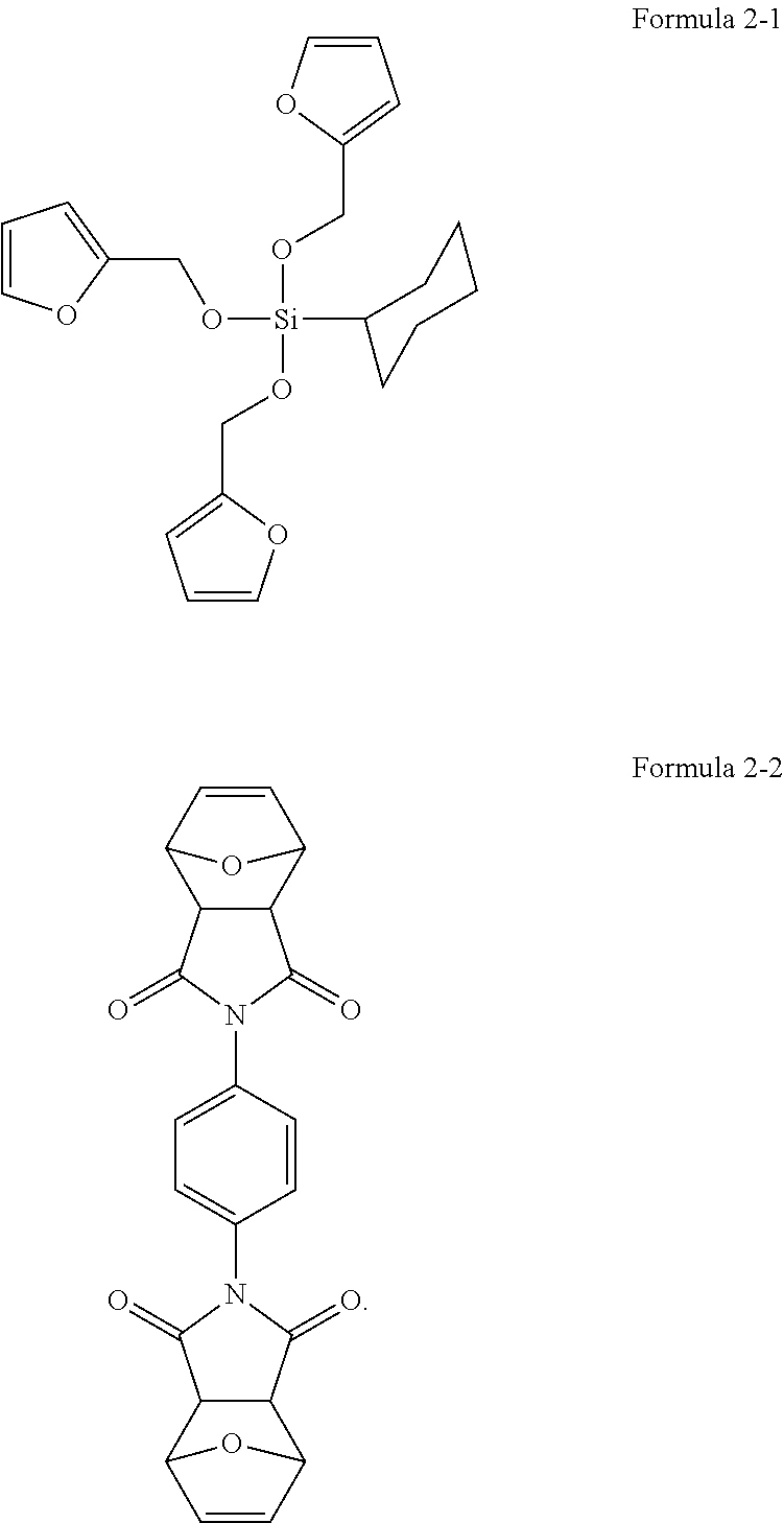
- the monomers may include compounds represented by Formulae 2-1 and 2-2 below:
- the Diels-Alder polymer may include a polyphthalaldehyde (PPA) polymer, or a polymer of a bis(maleimide) derivative cross-linked by trioxysilane.
- PPA polyphthalaldehyde
- a polymer of a bis(maleimide) derivative cross-linked by trioxysilane may include a polyphthalaldehyde (PPA) polymer, or a polymer of a bis(maleimide) derivative cross-linked by trioxysilane.
- the Diels-Alder polymer may include a polymer represented by Formula 1 below:
- R 1 is a hydrogen atom, a C 1 -C 10 alkyl group, or a C 6 -C 20 aryl group
- R 2 to R 4 are each independently a hydrogen atom, a halogen atom, or a C 1 -C 10 alkyl group
- n is an integer equal to or greater than 10 and equal to or less than 1,000.
- the Diels-Alder polymer may include a polymer represented by Formula 2 below:
- the method may further include forming a transfer layer on the bank layer pattern.
- the method may further include forming a heat insulating layer between the reflection layer pattern and the light absorbing layer.
- the light absorbing layer may include a metal layer or a stack structure in which metal layers and metal oxide layers are alternately stacked.
- the light absorbing layer may absorb the light and convert the light into heat.
- the light may be a flash lamp light, laser light, or light-emitting diode (LED) light.
- LED light-emitting diode
- the light may be projected to increase a temperature of the bank layer in the second regions to be greater than a depolymerization temperature of the Diels-Alder polymer.
- FIG. 1 illustrates a schematic cross-sectional view of an optical pattern transfer mask according to an exemplary embodiment
- FIGS. 2 and 3 illustrate schematic cross-sectional views illustrating stages of a method of forming a patterned transfer layer on a device substrate by using the optical pattern transfer mask of FIG. 1 ;
- FIG. 4 illustrates a schematic cross-sectional view of an optical pattern transfer mask according to another exemplary embodiment
- FIGS. 5 and 6 illustrate schematic cross-sectional views for describing stages of a method of forming a patterned transfer layer on the device substrate by using the optical pattern transfer mask of FIG. 4 ;
- FIGS. 7A to 7D illustrate cross-sectional views for sequentially describing stages of a method of fabricating the optical pattern transfer mask of FIG. 1 ;
- FIGS. 8A to 8D illustrate cross-sectional views for sequentially describing stages of a method of fabricating the optical pattern transfer mask of FIG. 4 ;
- FIG. 9 illustrates a schematic cross-sectional view of an organic light-emitting display apparatus fabricated using any one of the optical pattern transfer masks of FIGS. 1 and 4 .
- FIG. 1 illustrates a schematic cross-sectional view of an optical pattern transfer mask 100 according to an exemplary embodiment.
- the optical pattern transfer mask 100 may include a light transmissive substrate 101 , a reflection layer pattern 110 , a heat insulation layer 120 , a light absorbing layer 130 , and a bank layer pattern 140 .
- the light transmissive substrate 101 may be formed of a suitable light transmittable material.
- the light transmissive substrate 101 may be formed of a glass material or a heat resistant plastic material.
- the light transmissive substrate 101 has a plurality of first regions A 1 and a plurality of second regions A 2 .
- One second region A 2 may be formed between every two adjacent first regions A 1 .
- the reflection layer pattern 110 may be disposed on the light transmissive substrate 101 to correspond to the plurality of first regions A 1 .
- the reflection layer pattern 110 may reflect light incident on the reflection layer pattern 110 .
- the reflection layer pattern may include a metal having a high reflectance, such as Ag, Al, Pt, Pd, Au, Ni, Nd, or Ir.
- the reflection layer pattern 110 disposed in the first regions A 1 may reflect light incident from the bottom surface of the light transmissive substrate 101 . Accordingly, light may not be incident on layers in the first regions A 1 beyond the reflection layer pattern 110 in a direction away from the bottom surface of the light transmissive substrate 101 , and light may be incident only on such layers in the second regions A 2 .
- the heat insulation layer 120 may be in contact with the light absorbing layer 130 to prevent heat generated by the light absorbing layer 130 after absorbing the light from being transferred to the light transmissive substrate 101 instead being transferred to a transfer layer. Thereby, the heat insulation layer 120 may inhibit heat loss or deterioration of the light transmissive substrate 101 .
- the heat insulation layer 120 may be formed of a material having a lower thermal conductivity than that of the light absorbing layer 130 and having a high light transmittance.
- the heat insulation layer 120 may be formed of a heat resistant polymer or an inorganic material.
- the heat resistant polymer may include: a high temperature polyimide; a thermosetting heat resistant polymer formed of benzocyclobutene, trifluorovinyltether, chlorosilane, or an ethynyl group containing compound; a photocrosslinkable heat resistant polymer formed of an oxetane compound or a cinnamate compound; or an organic siloxane-based heat resistant polymer.
- the inorganic material may be titanium oxide, silicon oxide, silicon nitroxide, zirconium oxide, silicon carbide, or the like.
- the light absorbing layer 130 may be formed on the heat insulation layer 120 to cover the entire surface of the light transmissive substrate 101 .
- the light absorbing layer 130 absorbs light, thereby generating heat such that a transfer layer (e.g., 150 in FIG. 2 ) formed thereon is transferred to a device substrate.
- a transfer layer e.g., 150 in FIG. 2
- portions of the light absorbing layer 130 corresponding to the first regions A 1 are screened by the reflection layer 110 so as not to absorb light and generate heat.
- other portions of the light absorbing layer 130 corresponding to the second regions A 2 are not screened by the reflection layer pattern 110 so as to absorb light and generate heat.
- the transfer layer 150 corresponding to the second regions A 2 may be transferred onto the device substrate.
- the light absorbing layer 130 may have a single-layered structure including carbon or metal, or a multi-layered structure in which metal layers and metal oxide layers are alternately stacked.
- the metal may include Mo, Cr, Ti, or W.
- the metal oxide may include, for example, ITO or SiO 2 .
- the light absorbing layer 130 may have a metal/metal oxide/metal stack structure.
- the bank layer pattern 140 may be disposed on the light absorbing layer 130 in the first regions A 1 .
- the bank layer pattern 140 may serve as a screen to prevent spreading of the transfer layer 150 into other regions when the transfer layer 150 in the second regions A 2 is separated from the optical pattern transfer mask by thermal energy and transferred to the device substrate. The transfer may be performed while the optical pattern transfer mask is spaced apart from the device substrate by a predetermined distance. If the bank layer pattern 140 were not present, a material constituting the transfer layer 150 might not be moved vertically but could instead spread in other directions. The bank layer pattern 140 may prevent the spread of the materials constituting the transfer layer 150 in other directions.
- the bank layer pattern 140 may be formed of a Diels-Alder polymer that may be polymerized or depolymerized by reversible Diels-Alder reaction.
- the Diels-Alder polymer according to an exemplary embodiment may be polymerized by a forward Diels-Alder reaction and may be depolymerized by a reverse Diels-Alder reaction.
- the Diels-Alder polymer may include a polyphthalaldehyde (PPA) polymer, or a bis(maleimide) derivative polymer cross-linked by trioxysilane.
- PPA polyphthalaldehyde
- PDA bis(maleimide) derivative polymer cross-linked by trioxysilane.
- the Diels-Alder polymer may include a polymer represented by Formula 1 or 2 below.
- R 1 is a hydrogen atom, a C 1 -C 10 alkyl group, or a C 6 -C 20 aryl group
- R 2 to R 4 are each independently a hydrogen atom, a halogen atom, or a C 1 -C 10 alkyl group.
- n may be is an integer equal to or greater than 10 and equal to or less than 1,000.
- the polymer represented by Formula 1 and the polymer represented by Formula 2 may have a molecular weight (number average molecular weight) of about 2,000 to about 4,000.
- a transfer layer 150 may be disposed on the light absorbing layer 130 and the bank layer pattern 140 of the optical pattern transfer mask.
- the transfer layer 150 is a layer including a material to be transferred to a device substrate later.
- the transfer layer 150 may include an organic material or an inorganic material.
- the transfer layer 150 may be a buffer layer used to form an emission layer or a resonance structure.
- FIGS. 2 and 3 illustrate schematic cross-sectional views of stages of a method of forming a patterned transfer layer on a device substrate 10 by using the optical pattern transfer mask 100 of FIG. 1 .
- the optical pattern transfer mask 100 and the device substrate 10 onto which the transfer layer 150 is transferred may be aligned as illustrated in FIG. 2 .
- the optical pattern transfer mask 100 and the device substrate 10 may be spaced apart from each other at a predetermined distance.
- the optical pattern transfer mask 100 and the device substrate 10 may be aligned to be in a close contact with each other, if desired.
- light may be projected onto one surface of the light transmissive substrate 101 of the optical pattern transfer mask 100 opposite to the device substrate 10 , as illustrated in FIG. 2 . While light projected onto the first regions A 1 is reflected by the reflection layer pattern 110 and fails to reach the light absorbing layer 130 in the first regions A 1 , light projected onto the second regions A 2 between the first regions A 1 passes through the heat insulation layer 120 to reach the light absorbing layer 130 in the second regions A 2 . Thus, light may be converted into heat in the light absorbing layer 130 in the second regions A 2 between the first regions A 1 .
- Heat generated in the light absorbing layer 130 is transferred to the transfer layer 150 .
- heat is not transferred to the entire transfer layer 150 .
- heat is transferred to portions of the transfer layer 150 corresponding to the second regions A 2 between the first regions A 1 .
- Heat may not be generated in portions of the light absorbing layer 130 corresponding to the first regions A 1 due to the reflection layer pattern 110 disposed in the plurality of the first regions A 1 .
- Portions of the transfer layer 150 corresponding to the second regions A 2 between the first regions A 1 may be transferred to the device substrate 10 as illustrated in FIG. 3 , so that a transfer layer pattern 20 may be formed on the device substrate 10 .
- the transfer layer 150 of the optical pattern transfer mask 100 may be transferred to the device substrate 10 by aligning the optical pattern transfer mask 100 and the device substrate 10 and projecting light onto the back surface of the optical pattern transfer mask 100 , thereby forming the transfer layer pattern 20 .
- the bank layer pattern 140 may serve as a screen to prevent spreading of the transfer layer in directions other than the vertical direction when the transfer layer 150 of the second regions A 2 is separated from the optical pattern transfer mask 100 and transferred to the device substrate 10 .
- the bank layer pattern 140 may prevent a material constituting the transfer layer 150 from being transferred to unintended regions on the device substrate 10 . Thus, the material may be transferred only to an intended region.
- FIG. 4 illustrates a schematic cross-sectional view of an optical pattern transfer mask 200 according to another exemplary embodiment.
- the optical pattern transfer mask 200 differs from the optical pattern transfer mask 100 described above with reference to FIG. 1 , in that the optical pattern transfer mask 200 does not include a heat insulation layer 120 .
- the heat insulation layer 120 may prevent heat generated by the light absorbing layer 130 from being transferred to the light transmissive substrate 101 instead of to the transfer layer 150 . Thereby, the heat insulation layer 120 may inhibit heat loss or deterioration of the light transmissive substrate 101 . However, the heat insulation layer 120 may be omitted, and the bank layer pattern 140 may be formed on the light absorbing layer 230 according to the present embodiment.
- FIGS. 5 and 6 illustrate schematic cross-sectional views for describing stages of a method of forming a patterned transfer layer on the device substrate 10 by using the optical pattern transfer mask 200 of FIG. 4 .
- the transfer layer 150 of the optical pattern transfer mask 200 may be transferred to the device substrate 10 by aligning the optical pattern transfer mask 200 and the device substrate 10 and projecting light onto the back surface of the optical pattern transfer mask 200 , thereby forming the transfer layer pattern 20 as described above with reference to FIGS. 2 and 3 .
- FIGS. 7A to 7D illustrate cross-sectional views for sequentially describing stages of a method of fabricating the optical pattern transfer mask 100 of FIG. 1 .
- the reflection layer pattern 110 may be formed on the light transmissive substrate 101 .
- the light transmissive substrate 101 may be formed of a suitable light transmittable material.
- the light transmissive substrate 101 may be formed of a glass material or a heat resistant plastic material.
- the light transmissive substrate 101 has a plurality of first regions A 1 and a second region A 2 between the first regions A 1 .
- the reflection layer pattern 110 may be formed on the light transmissive substrate 101 to correspond to the plurality of first regions A 1 .
- the reflection layer pattern 110 may be formed of a metal having a high reflectance, such as Ag, Al, Pt, Pd, Au, Ni, Nd, or Ir.
- the reflection layer pattern 110 may be formed by forming a layer by sputtering, vacuum deposition, or the like, and forming a pattern by lithography, or the like.
- the reflection layer pattern 110 may have a thickness of, for example, about 50 nm to about 500 nm.
- the heat insulation layer 120 may be formed on the light transmissive substrate 101 and the reflection layer pattern 110 .
- the heat insulation layer 120 may be formed of a heat resistant polymer or an inorganic material, as described above with reference to FIG. 1 .
- the heat insulation layer 120 may be formed by a general solution coating method such as spin coating and bar coating or deposition.
- the heat insulation layer 120 may have a thickness of about 500 nm to about 3 ⁇ m.
- the light absorbing layer 130 may be formed on the heat insulation layer 120 to cover the entire surface of the light transmissive substrate 101 .
- the light absorbing layer 130 may have a single-layered structure including carbon or metal or a multi-layered structure in which metal layers and metal oxide layers are alternately stacked.
- the metal may include Mo, Cr, Ti, or W.
- the metal oxide may include ITO and SiO 2 .
- the light absorbing layer 130 may have a metal/metal oxide/metal stack structure.
- a bank layer 140 ′ may be formed on the light absorbing layer 130 .
- the bank layer 140 ′ may be formed of a Diels-Alder polymer that may be polymerizable or depolymerizable by reversible Diels-Alder reaction.
- the bank layer 140 ′ may be formed of a polyphthalaldehyde (PPA) polymer, or a polymer of a bis(maleimide) derivative cross-linked by trioxysilane.
- PPA polyphthalaldehyde
- the bank layer 140 ′ may be formed of a polyphthalaldehyde (PPA) polymer, or a polymer of a bis(maleimide) derivative cross-linked by trioxysilane.
- the PPA polymer may be represented by Formula 1 below.
- R 1 is a hydrogen atom, a C 1 -C 10 alkyl group, or a C 6 -C 20 aryl group
- R 2 to R 4 are each independently a hydrogen atom, a halogen atom, or a C 1 -C 10 alkyl group.
- n may be an integer equal to or greater than 10.
- the polymer represented by Formula 1 may have a molecular weight (number average molecular weight) of about 2,000 to about 4,000.
- the polymer of a bis(maleimide) derivative cross-linked by trioxysilane may be represented by Formula 2 below.
- the polymer represented by Formula 2 may have a molecular weight of about 2,000 to about 4,000.
- the bank layer 140 ′ may be formed, for example, by applying a coating on the light absorbing layer 130 including a composition in which monomers capable of forming the Diels-Alder polymer are dissolved or dispersed, and polymerizing the monomers by the Diels-Alder reaction while heating the applied composition.
- a Diels-Alder polymer represented by Formula 1a below may be formed through a reaction scheme below.
- a heating temperature may be in a range of about 100° C. to about 250° C.
- TCAI is trichloroacetyl isocyanate.
- a Diels-Alder polymer represented by Formula 2 may be formed through a reaction scheme shown below.
- a heating temperature may be in a range of about 100° C. to about 250° C.
- the light may be flash lamp light, laser light, or LED light.
- the light may be projected such that a temperature of the bank layer 140 ′ is greater than a depolymerization temperature of the Diels-Alder polymer.
- portions of the light absorbing layer 130 corresponding to the second regions A 2 exposed through the reflection layer pattern 110 may absorb the light, thereby generating heat.
- the bank layer 140 ′ may be heated by the generated heat in the second regions A 2 , and thus a reverse Diels-Alder reaction may occur.
- the polymer in the second regions A 2 may be removed by depolymerization and decomposition into small molecules.
- the decomposed small molecules in a gas state may be removed by a vacuum pump or the like.
- the polymer of the bank layer 140 ′ in the first regions A 1 is not heated. Accordingly, the reverse Diels-Alder reaction does not occur in the first regions A 1 , and thus the polymer in the first regions A 1 may not be depolymerized but may remain thereon.
- the polymer of the bank layer 140 ′ remains in the first regions A 1 and is removed from the second regions A 2 where the bank layer pattern 140 is formed.
- FIGS. 8A to 8D illustrate cross-sectional views for sequentially describing a method of fabricating the optical pattern transfer mask 200 of FIG. 4 .
- the method of fabricating the optical pattern transfer mask 200 may be the same as that of fabricating the optical pattern transfer mask 100 described above with reference to FIGS. 7A to 7D , except that the heat insulation layer 120 is not formed.
- the present embodiment will be described based on differences from the method of fabricating the optical pattern transfer mask described above with reference to FIGS. 7A to 7D .
- the reflection layer pattern 110 may be formed on the light transmissive substrate 101 . Formation of the light transmissive substrate 101 and the reflection layer pattern 110 is described above with reference to FIG. 7A .
- a light absorbing layer 230 may be formed on the light transmissive substrate 101 and the reflection layer pattern 110 .
- the light absorbing layer 230 may have a single-layered structure including carbon or metal or a multi-layered structure in which metal layers and metal oxide layers are alternately stacked in the same manner as in the light absorbing layer 130 described above with reference to FIG. 7B .
- the light absorbing layer 230 may have a thickness of about 100 ⁇ m to about 500 ⁇ m.
- the bank layer 140 ′ may be formed on the light absorbing layer 230 . Formation of the bank layer 140 ′ is described above with reference to FIG. 7C .
- the polymer of the bank layer 140 ′ remains in the first regions A 1 and is removed in the second regions A 2 , thereby forming the bank layer pattern 140 .
- FIG. 9 illustrates a schematic cross-sectional view of an organic light-emitting display apparatus fabricated using any one of the optical pattern transfer masks of FIGS. 1 and 4 .
- various constituent elements of the organic light-emitting display apparatus may be formed on a substrate 50 .
- the substrate 50 may be the device substrate 10 described above with reference to FIG. 2 or a cut portion of the device substrate 10 .
- the substrate 50 may be formed of a transparent material such as a glass material, a plastic material, or a metallic material.
- a common layer such as a buffer layer 51 , a gate insulating layer 53 , or an interlayer insulating layer 55 , may be formed on the entire surface of the substrate 50 .
- a patterned semiconductor layer 52 including a channel region 52 a , a source contact region 52 b , and a drain contact region 52 c may be formed, and a gate electrode 54 , a source electrode 56 , and a drain electrode 57 constituting a thin film transistor (TFT) may be formed together with the patterned semiconductor layer 52 .
- TFT thin film transistor
- a passivation layer 58 to cover the TFT and a planarization layer 59 disposed on the passivation layer 58 and having a planar upper surface may be formed on the entire surface of the substrate 50 .
- An organic light-emitting device (OLED) which includes a patterned pixel electrode 61 , an opposite electrode 63 corresponding to almost the entire surface of the substrate 50 , and a multi-layered intermediate layer 62 interposed between the pixel electrode 61 and the opposite electrode 63 and including an emission layer, may be formed on the planarization layer 59 .
- the intermediate layer 62 may include a common layer corresponding to almost the entire surface of the substrate and a pattern layer patterned to corresponding to the pixel electrode 61 .
- the pixel electrode 61 may be electrically connected to the TFT.
- a pixel defining layer 60 that covers edges of the pixel electrode 62 and includes openings defining each pixel region, may be formed to correspond to almost the entire surface of the substrate 50 .
- the constituent elements may be formed using the optical pattern transfer mask according to exemplary embodiments.
- the intermediate layer 62 may be formed using the optical pattern transfer mask according to exemplary embodiments.
- a hole injection layer (HIL), a hole transport layer (HTL), an emission layer (EML), an electron transport layer (ETL), an electron injection layer (EIL), or the like included in the intermediate layer 62 may be formed according to the method according to exemplary embodiments.
- the optical pattern transfer mask according to exemplary embodiments may also be used to form another pattern layer.
- An optical pattern transfer mask has been described above.
- other transfer methods such as one using a photo-thermal conversion transfer mask may be used.
- Such transfer methods include aligning an optical pattern transfer mask and a substrate onto which a layer is transferred, and forming a transfer layer patterned to correspond to regions between a plurality of first regions of the optical pattern transfer mask on the substrate by projecting light onto the optical pattern transfer mask as described above.
- the bank layer pattern may be formed by back exposure by using the reflection layer pattern as an exposure mask.
- the bank layer pattern may be formed by a simple process with low manufacturing costs without performing photolithography.
- the emission layer may be manufactured using various methods, such as a transfer printing process or inkjet printing.
- a bank pattern may be used to prevent an undesired transfer of a pattern, which is used for transferring a transfer material from the optical pattern transfer mask, onto an unintended transfer region of a device substrate.
- the bank pattern may be formed by photolithography after forming an inorganic layer, photolithography is a complicated and expensive process.
- Embodiments provide an optical pattern transfer mask including a bank pattern formed by using a simple process with low manufacturing costs and methods of fabricating the optical pattern transfer masks.
Landscapes
- Physics & Mathematics (AREA)
- General Physics & Mathematics (AREA)
- Engineering & Computer Science (AREA)
- Manufacturing & Machinery (AREA)
- Spectroscopy & Molecular Physics (AREA)
- Optics & Photonics (AREA)
- Microelectronics & Electronic Packaging (AREA)
- Electroluminescent Light Sources (AREA)
Abstract
Description

wherein, in

wherein R1 is a hydrogen atom, a C1-C10 alkyl group, or a C6-C20 aryl group, R2 to R4 are each independently a hydrogen atom, a halogen atom, or a C1-C10 alkyl group, and n is an integer equal to or greater than 10 and equal to or less than 1,000.


Claims (18)


Applications Claiming Priority (2)
| Application Number | Priority Date | Filing Date | Title |
|---|---|---|---|
| KR1020140125248A KR20160034529A (en) | 2014-09-19 | 2014-09-19 | Optical pattern transfer mask and method for fabricating the same |
| KR10-2014-0125248 | 2014-09-19 |
Publications (2)
| Publication Number | Publication Date |
|---|---|
| US20160085146A1 US20160085146A1 (en) | 2016-03-24 |
| US9448472B2 true US9448472B2 (en) | 2016-09-20 |
Family
ID=55525638
Family Applications (1)
| Application Number | Title | Priority Date | Filing Date |
|---|---|---|---|
| US14/640,512 Expired - Fee Related US9448472B2 (en) | 2014-09-19 | 2015-03-06 | Optical pattern transfer mask and method of fabricating the same |
Country Status (2)
| Country | Link |
|---|---|
| US (1) | US9448472B2 (en) |
| KR (1) | KR20160034529A (en) |
Families Citing this family (3)
| Publication number | Priority date | Publication date | Assignee | Title |
|---|---|---|---|---|
| EP3724369A4 (en) * | 2017-12-14 | 2021-12-22 | Boe Technology Group Co., Ltd. | DONOR SUBSTRATE FOR DEPOSITING A DEPOSITORY MATERIAL ON ACCEPTOR SUBSTRATE, METHOD FOR DEPOSITING A DEPOSITIVE MATERIAL AND METHOD FOR MANUFACTURING A DONOR SUBSTRATE |
| CN108598132A (en) * | 2018-05-23 | 2018-09-28 | 京东方科技集团股份有限公司 | The production method of display base plate, the production method of mask plate, display device |
| CN110667277A (en) * | 2019-10-11 | 2020-01-10 | 厦门市三升标饰印刷有限公司 | Manufacturing process and using method of label roll |
Citations (10)
| Publication number | Priority date | Publication date | Assignee | Title |
|---|---|---|---|---|
| JP2008106213A (en) | 2006-09-25 | 2008-05-08 | Fujifilm Corp | Laser decomposable resin composition and pattern forming material using the same |
| US20090104835A1 (en) | 2007-10-23 | 2009-04-23 | Semiconductor Energy Laboratory Co., Ltd. | Method of Manufacturing Light-Emitting Device, and Evaporation Donor Substrate |
| US20090197017A1 (en) * | 2008-02-04 | 2009-08-06 | Semiconductor Energy Laboratory Co., Ltd. | Deposition Method and Method for Manufacturing Light-Emitting Device |
| US20090220706A1 (en) * | 2008-02-29 | 2009-09-03 | Semiconductor Energy Laboratory Co., Ltd. | Film-Formation Method and Manufacturing Method of Light-Emitting Device |
| US20090325451A1 (en) | 2008-06-25 | 2009-12-31 | Sony Corporation | Donor substrate and method of manufacturing display |
| US20100015424A1 (en) * | 2008-07-21 | 2010-01-21 | Semiconductor Energy Laboratory Co., Ltd. | Deposition Donor Substrate and Method for Manufacturing Light-Emitting Device |
| US20100084676A1 (en) | 2008-10-08 | 2010-04-08 | Hitachi Displays, Ltd. | Organic el display device and manufacturing method thereof |
| WO2011125570A1 (en) | 2010-03-31 | 2011-10-13 | 東レ株式会社 | Donor substrate for transfer, device manufacturing method and organic el element |
| US20120301672A1 (en) | 2010-09-30 | 2012-11-29 | International Business Machines Corporation | Patterning nano-scale patterns on a film comprising unzipping copolymers |
| KR20130098655A (en) | 2012-02-28 | 2013-09-05 | 엘지디스플레이 주식회사 | Thin film transistor substrate and method of fabricating the same |
-
2014
- 2014-09-19 KR KR1020140125248A patent/KR20160034529A/en not_active Withdrawn
-
2015
- 2015-03-06 US US14/640,512 patent/US9448472B2/en not_active Expired - Fee Related
Patent Citations (12)
| Publication number | Priority date | Publication date | Assignee | Title |
|---|---|---|---|---|
| JP2008106213A (en) | 2006-09-25 | 2008-05-08 | Fujifilm Corp | Laser decomposable resin composition and pattern forming material using the same |
| US20090104835A1 (en) | 2007-10-23 | 2009-04-23 | Semiconductor Energy Laboratory Co., Ltd. | Method of Manufacturing Light-Emitting Device, and Evaporation Donor Substrate |
| US20090197017A1 (en) * | 2008-02-04 | 2009-08-06 | Semiconductor Energy Laboratory Co., Ltd. | Deposition Method and Method for Manufacturing Light-Emitting Device |
| US20090220706A1 (en) * | 2008-02-29 | 2009-09-03 | Semiconductor Energy Laboratory Co., Ltd. | Film-Formation Method and Manufacturing Method of Light-Emitting Device |
| US20090325451A1 (en) | 2008-06-25 | 2009-12-31 | Sony Corporation | Donor substrate and method of manufacturing display |
| JP2010034022A (en) | 2008-06-25 | 2010-02-12 | Sony Corp | Donor substrate, and manufacturing method of display |
| US20100015424A1 (en) * | 2008-07-21 | 2010-01-21 | Semiconductor Energy Laboratory Co., Ltd. | Deposition Donor Substrate and Method for Manufacturing Light-Emitting Device |
| US20100084676A1 (en) | 2008-10-08 | 2010-04-08 | Hitachi Displays, Ltd. | Organic el display device and manufacturing method thereof |
| WO2011125570A1 (en) | 2010-03-31 | 2011-10-13 | 東レ株式会社 | Donor substrate for transfer, device manufacturing method and organic el element |
| KR20120112585A (en) | 2010-03-31 | 2012-10-11 | 도레이 카부시키가이샤 | Donor substrate for transfer, device manufacturing method and organic el element |
| US20120301672A1 (en) | 2010-09-30 | 2012-11-29 | International Business Machines Corporation | Patterning nano-scale patterns on a film comprising unzipping copolymers |
| KR20130098655A (en) | 2012-02-28 | 2013-09-05 | 엘지디스플레이 주식회사 | Thin film transistor substrate and method of fabricating the same |
Non-Patent Citations (3)
| Title |
|---|
| Coulembier et al., Probe-Based Nanolithography: Self-Amplified Depolymerization Media for Dry Lithography, Macromolecules 2010, 43, Dec. 11, 2009; pp. 572-574. |
| Gotsmann et al., Exploiting Chemical Switching in a Diels-Alder Polymer for nanoscale Probe Lithography and Data Storage, Adv. Funct. Mater, 2006, 16, pp. 1499-1505. |
| Knoll et al. Probe-Based 3-D Nanolithograpy Using Self-Amplified Depolymerization Polymers, Adv. Mater, 2010, 22, pp. 3361-3365. |
Also Published As
| Publication number | Publication date |
|---|---|
| US20160085146A1 (en) | 2016-03-24 |
| KR20160034529A (en) | 2016-03-30 |
Similar Documents
| Publication | Publication Date | Title |
|---|---|---|
| Xie et al. | Inkjet‐printed high‐efficiency multilayer QLEDs based on a novel crosslinkable small‐molecule hole transport material | |
| USRE50670E1 (en) | Electroluminescence display device | |
| JP5417854B2 (en) | Photosensitive composition for partition walls of active drive type organic electroluminescent device and active drive type organic electroluminescent display device | |
| US8174179B2 (en) | Organic light emitting display apparatus | |
| KR101570899B1 (en) | Method for manufacturing device having hole injection/transport layer | |
| TWI321822B (en) | Transfer substrate, transfer method, and method of manufacturing display device | |
| KR101011428B1 (en) | Buffer layer for organic electroluminescent device, manufacturing method and use thereof | |
| JP5428910B2 (en) | Photosensitive composition for partition walls of active drive type organic electroluminescent device and active drive type organic electroluminescent display device | |
| US9093397B2 (en) | Flexible device manufacturing method and flexible device | |
| KR101156436B1 (en) | Optical film and organic light emitting display apparatus having the same | |
| EP3021374B1 (en) | Transparent display devices and methods of manufacturing the same | |
| CN110649071A (en) | Organic light emitting diode display, electronic device including the same, and manufacturing method thereof | |
| US20170352837A1 (en) | Display apparatus and method of manufacturing the same | |
| CN104183783A (en) | Organic light emitting display device with flexible substrate | |
| JP2014120218A (en) | Method for manufacturing organic el display device | |
| TW201308705A (en) | Organic light emitting device and method of manufacturing same | |
| KR20130043482A (en) | Organic light emitting display device | |
| US9448472B2 (en) | Optical pattern transfer mask and method of fabricating the same | |
| KR102442188B1 (en) | Organic luminescence emitting display device and the method of manufacturing the same | |
| KR101803724B1 (en) | Organic light emitting structure, method of manufacturing an organic light emitting structure, organic light emitting display device and method of manufacturing an organic light emitting display device | |
| Jang et al. | Tetrabranched photo-crosslinker enables micrometer-scale patterning of light-emitting super yellow for high-resolution OLEDs | |
| JP2012089474A (en) | Display device | |
| KR20060111672A (en) | Thermal Transfer Method of Luminescent Dendrimer | |
| JP5244378B2 (en) | Organic light emitting display | |
| WO2013104202A1 (en) | Amoled device and manufacturing method |
Legal Events
| Date | Code | Title | Description |
|---|---|---|---|
| AS | Assignment |
Owner name: SAMSUNG DISPLAY CO., LTD., KOREA, REPUBLIC OF Free format text: ASSIGNMENT OF ASSIGNORS INTEREST;ASSIGNOR:KWON, YOUNGGIL;REEL/FRAME:035103/0207 Effective date: 20150227 |
|
| FEPP | Fee payment procedure |
Free format text: PAYOR NUMBER ASSIGNED (ORIGINAL EVENT CODE: ASPN); ENTITY STATUS OF PATENT OWNER: LARGE ENTITY |
|
| STCF | Information on status: patent grant |
Free format text: PATENTED CASE |
|
| FEPP | Fee payment procedure |
Free format text: MAINTENANCE FEE REMINDER MAILED (ORIGINAL EVENT CODE: REM.); ENTITY STATUS OF PATENT OWNER: LARGE ENTITY |
|
| LAPS | Lapse for failure to pay maintenance fees |
Free format text: PATENT EXPIRED FOR FAILURE TO PAY MAINTENANCE FEES (ORIGINAL EVENT CODE: EXP.); ENTITY STATUS OF PATENT OWNER: LARGE ENTITY |
|
| STCH | Information on status: patent discontinuation |
Free format text: PATENT EXPIRED DUE TO NONPAYMENT OF MAINTENANCE FEES UNDER 37 CFR 1.362 |
|
| FP | Lapsed due to failure to pay maintenance fee |
Effective date: 20200920 |