US9437537B2 - Semiconductor device and method of manufacturing the same - Google Patents
Semiconductor device and method of manufacturing the same Download PDFInfo
- Publication number
- US9437537B2 US9437537B2 US13/571,524 US201213571524A US9437537B2 US 9437537 B2 US9437537 B2 US 9437537B2 US 201213571524 A US201213571524 A US 201213571524A US 9437537 B2 US9437537 B2 US 9437537B2
- Authority
- US
- United States
- Prior art keywords
- lines
- semiconductor device
- patterns
- line
- dummy
- Prior art date
- Legal status (The legal status is an assumption and is not a legal conclusion. Google has not performed a legal analysis and makes no representation as to the accuracy of the status listed.)
- Active, expires
Links
Images


Classifications
-
- H—ELECTRICITY
- H10—SEMICONDUCTOR DEVICES; ELECTRIC SOLID-STATE DEVICES NOT OTHERWISE PROVIDED FOR
- H10P—GENERIC PROCESSES OR APPARATUS FOR THE MANUFACTURE OR TREATMENT OF DEVICES COVERED BY CLASS H10
- H10P76/00—Manufacture or treatment of masks on semiconductor bodies, e.g. by lithography or photolithography
- H10P76/20—Manufacture or treatment of masks on semiconductor bodies, e.g. by lithography or photolithography of masks comprising organic materials
- H10P76/204—Manufacture or treatment of masks on semiconductor bodies, e.g. by lithography or photolithography of masks comprising organic materials of organic photoresist masks
-
- H01L23/522—
-
- H—ELECTRICITY
- H10—SEMICONDUCTOR DEVICES; ELECTRIC SOLID-STATE DEVICES NOT OTHERWISE PROVIDED FOR
- H10W—GENERIC PACKAGES, INTERCONNECTIONS, CONNECTORS OR OTHER CONSTRUCTIONAL DETAILS OF DEVICES COVERED BY CLASS H10
- H10W20/00—Interconnections in chips, wafers or substrates
- H10W20/40—Interconnections external to wafers or substrates, e.g. back-end-of-line [BEOL] metallisations or vias connecting to gate electrodes
-
- H01L21/0337—
-
- H01L21/32139—
-
- H—ELECTRICITY
- H10—SEMICONDUCTOR DEVICES; ELECTRIC SOLID-STATE DEVICES NOT OTHERWISE PROVIDED FOR
- H10P—GENERIC PROCESSES OR APPARATUS FOR THE MANUFACTURE OR TREATMENT OF DEVICES COVERED BY CLASS H10
- H10P50/00—Etching of wafers, substrates or parts of devices
- H10P50/71—Etching of wafers, substrates or parts of devices using masks for conductive or resistive materials
-
- H—ELECTRICITY
- H10—SEMICONDUCTOR DEVICES; ELECTRIC SOLID-STATE DEVICES NOT OTHERWISE PROVIDED FOR
- H10P—GENERIC PROCESSES OR APPARATUS FOR THE MANUFACTURE OR TREATMENT OF DEVICES COVERED BY CLASS H10
- H10P76/00—Manufacture or treatment of masks on semiconductor bodies, e.g. by lithography or photolithography
- H10P76/40—Manufacture or treatment of masks on semiconductor bodies, e.g. by lithography or photolithography of masks comprising inorganic materials
- H10P76/408—Manufacture or treatment of masks on semiconductor bodies, e.g. by lithography or photolithography of masks comprising inorganic materials characterised by their sizes, orientations, dispositions, behaviours or shapes
- H10P76/4085—Manufacture or treatment of masks on semiconductor bodies, e.g. by lithography or photolithography of masks comprising inorganic materials characterised by their sizes, orientations, dispositions, behaviours or shapes characterised by the processes involved to create the masks
-
- H—ELECTRICITY
- H10—SEMICONDUCTOR DEVICES; ELECTRIC SOLID-STATE DEVICES NOT OTHERWISE PROVIDED FOR
- H10W—GENERIC PACKAGES, INTERCONNECTIONS, CONNECTORS OR OTHER CONSTRUCTIONAL DETAILS OF DEVICES COVERED BY CLASS H10
- H10W20/00—Interconnections in chips, wafers or substrates
- H10W20/40—Interconnections external to wafers or substrates, e.g. back-end-of-line [BEOL] metallisations or vias connecting to gate electrodes
- H10W20/41—Interconnections external to wafers or substrates, e.g. back-end-of-line [BEOL] metallisations or vias connecting to gate electrodes characterised by their conductive parts
- H10W20/43—Layouts of interconnections
-
- H01L2924/00—
-
- H01L2924/0002—
Definitions
- Embodiments of this disclosure relate to semiconductor devices and methods of manufacturing the same. Additionally, an embodiment of this disclosure relates to a semiconductor device including dummy patterns and a method of manufacturing the same.
- a semiconductor device requires wires for coupling elements. That is, wires for coupling gate lines (for example, word lines) and a peripheral circuit (for example, a row decoder) are formed through a process.
- gate lines for example, word lines
- peripheral circuit for example, a row decoder
- the gate lines are formed in parallel in one direction and are coupled to the decoder through contact plugs and the wires at the ends of the gate lines.
- the width of the gate line is gradually narrowed in order to increase the degree of integration.
- contact pads are formed at respective parts where the gate lines and the contact plugs are coupled. As the contact pads are formed, a coupling margin between the gate lines and the contact plugs are improved, and an increase in resistance or the occurrence of failure, resulting from an alignment error, can be prevented.
- a semiconductor device includes: conductive lines configured to include first lines extending generally in parallel in a first direction and second lines extending generally in parallel in a second direction to intersect the first direction from respective ends of the first lines and each second line having a width wider than the first line; and dummy patterns formed generally between the second lines.
- a method of manufacturing a semiconductor device includes: forming a target etch layer, a first hard mask layer, and a second hard mask layer over a semiconductor substrate; forming generally L-shaped auxiliary patterns and dummy auxiliary patterns, placed between second lines in a second direction and each formed to have an opening at a center of the dummy auxiliary pattern, on the second hard mask layer, wherein a first line in a first direction is coupled to the second line in the second direction at the generally L-shaped auxiliary pattern; forming first spacers on sidewalls of the auxiliary patterns and the dummy auxiliary patterns and removing the auxiliary patterns and the dummy auxiliary patterns; forming second hard mask patterns by etching the second hard mask layer by a first etch process employing the first spacers as an etch mask; forming second spacers on sidewalls of the second hard mask patterns and removing the second hard mask patterns; forming first hard mask patterns by etching the first hard mask layer by a second etch process employing
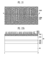
- FIG. 1 is a plan view illustrating a semiconductor device according to an embodiment of the present invention
- FIGS. 2A to 2J are diagrams illustrating a method of manufacturing the semiconductor device according to an example of an embodiment of the present invention.
- FIGS. 2Ab to 2Jb are cross sectional views, taken at points A to A′, of FIGS. 2A to 2J , respectively, and
- FIG. 3 is a diagram illustrating another example of a semiconductor device compared with the semiconductor device of FIG. 1 .
- ‘and/or’ represents that one or more of components arranged before and after ‘and/or’ is included.
- ‘connected/coupled’ represents that one component is directly coupled to another component or indirectly coupled through another component.
- a singular form may include a plural form as long as it is not specifically mentioned in a sentence.
- ‘include/comprise’ or ‘including/comprising’ used in the specification represents that one or more components, steps, operations, and elements exists or are added.
- FIG. 1 is a plane view illustrating a semiconductor device according to an embodiment of this invention.
- the semiconductor device may include a plurality of memory blocks, memory block one MB 1 and memory block 2 MB 2 .
- Each of the memory blocks MB 1 and MB 2 may include a plurality of conductive lines WL 0 to WL 31 which may be substantially bent into an L shape form, as shown in FIG. 1 .
- the conductive lines WL 0 to WL 31 may become gate lines or word lines.
- Each of the memory blocks MB 1 and MB 2 may further include conductive lines SSL and DSL formed on substantially the upper and lower sides of the plurality of conductive lines WL 0 to WL 31 and each may be formed to have a wider width than each of the lines WL 0 to WL 31 .
- the conductive lines SSL and DSL may become a source select lines and drain select lines, respectively.
- Each of the conductive lines WL 0 to WL 31 may include a first line L 1 extended in a first direction and a second line L 2 extended from the end of the first line L 1 in a second direction to substantially cross the first direction and may be formed to have a wider width than the first line L 1 .
- the conductive lines WL 0 to WL 31 of the memory block MB 1 and the conductive lines WL 0 to WL 31 of the memory block MB 2 may be rotated by 180 degrees and arranged so that they substantially overlap with each other in order to improve the degree of integration.
- dummy patterns DL may be formed between the conductive lines WL 0 to WL 31 in the second direction. This is also described in detail below.
- the conductive lines WL 0 to WL 31 may include the first lines L 1 extended in parallel in the first direction and the second lines L 2 extended from the respective ends of the first lines L 1 in parallel in the second direction to substantially cross the first direction.
- the first lines L 1 may have to have different lengths. That is, the ends of the first lines L 1 on one side may be aligned on the same line, and the ends of the first lines L 1 on the other side, coupled to the second lines L 2 , may be diagonally aligned. It is preferred that the ends of the second lines L 2 also be aligned on substantially the same line. Thus, the second lines L 2 may have different lengths. As a result, the substantially L-shaped conductive lines WL 0 to WL 31 may be gradually increased in length and arranged so that they substantially surround adjacent short conductive lines.
- each of the second lines L 2 may be wider than that of the first line L 1 and may be about twice the width of the first line L 1 .
- the second lines L 2 may include first patterns LP 1 extended in the second direction from the ends of the first lines L 1 and second patterns LP 2 formed substantially on the sidewalls of the first patterns LP 1 on one side or the other side.
- the first pattern LP 1 and the second pattern LP 2 each may have the same width as the first line L 1 . Accordingly, the width of the second line L 2 including the first and the second patterns LP 1 and LP 2 may be twice the width of the first line L 1 .
- the dummy patterns DL may be disposed substantially between the second lines L 2 and may be extended in the second direction. Also, the dummy patterns DL may not just be disposed between the second lines L 2 , but may be irregularly disposed between some of the second lines L 2 according to an example of a manufacturing method. For example, the dummy patterns DL may be disposed on one side and the other side of a line group LG including four of the second lines L 2 . That is, the dummy patterns DL may not be disposed between the second lines L 2 within the line group LG. Therefore, the dummy patterns DL may be disposed outside or on each side of the line group, before the first outer line of the line group and after a last outer line of the line group.
- the second pattern LP 2 may be a part of the dummy pattern DL, but the sidewall of the second pattern LP 2 may come in contact with the sidewall of the second line L 2 , thus becoming a part of the conductive line.
- the first lines L 1 may be arranged at substantially the same intervals and the second lines L 2 may be arranged at irregular intervals depending on the arrangement of the dummy patterns DL. That is, an interval between the second lines L 2 may be substantially identical to an interval between the first lines L 1 , and an interval between the second lines L 2 in areas where the dummy patterns DL are disposed are wider than an interval between the first lines L 1 .
- the second lines L 2 of the conductive lines WL 0 to WL 31 may be formed to have a wider width than the first lines L 1 as described above, and a contact plug may be formed on the second lines L 2 having a wider width without forming contact pads on the second lines L 2 .
- FIG. 3 is a diagram illustrating another example of a semiconductor device compared to the semiconductor device of FIG. 1 .
- an overall area may be increased and the number of process steps for forming the contact pads CPAD may be increased in order to maintain an interval between the contact pads CPAD. Furthermore, since patterns may not be formed in some areas, pattern density may become irregular. Consequently, process characteristics may deteriorate and there may be a high possibility that failure may occur.
- the occurrence of failure may be prevented because a manufacturing process may be uniformly applied to substantially all areas.
- the contact plug may be formed on the second lines L 2 without contact pads. Accordingly, a manufacturing process may be simplified because a process of forming the contact pads may be obviated. Furthermore, process reappearance may be secured, and reliability due to reduced failure may be improved.
- FIGS. 2A to 2J and 2Ab to 2Jb are diagrams illustrating the method of manufacturing the semiconductor device according to an embodiment of this invention.
- a target etch layer 203 , a first hard mask layer 205 , and a second hard mask layer 207 may be formed over a semiconductor substrate 201 .
- the target etch layer 203 may include a tunnel insulating layer 203 A, a first silicon layer 203 B, a dielectric layer 203 C, a second silicon layer 203 D, and a third hard mask layer 203 E.
- the first and the second hard mask layers 205 and 207 preferably are made of different materials so that they are not substantially etched by the same etchant.
- the first and the third hard mask layers 205 and 203 E preferably are made of different materials so that they are not substantially etched by the same etchant.
- the second and the third hard mask layers 207 and 203 E, respectively, may be made of the same material.
- Auxiliary patterns 209 M and dummy auxiliary patterns 209 D may be formed on the second hard mask layer 207 .
- Each of the auxiliary patterns 209 M may include a first line L 1 extended in a first direction and a second line L 2 extended in a second direction forming substantially an L shape form.
- An opening 209 H may be formed at the center of the second line L 2 and may be formed in a line form in the second direction.
- the dummy auxiliary patterns 209 D may be formed substantially between the second lines L 2 of the auxiliary patterns 209 M. Two dummy auxiliary patterns 209 D may be regularly formed between the second lines L 2 in parallel or substantially in parallel, but they may have different lengths.
- first spacers 211 M may be formed on the sidewalls of the auxiliary patterns 209 M and the dummy auxiliary patterns 209 D. Additionally, after forming an insulating layer substantially over the entire surface, a blanket etch process may be performed so that the insulating layer remains only on the sidewalls of the auxiliary patterns 209 M and the dummy auxiliary patterns 209 D. It may be preferred that the insulating layer be made of a different material from the first hard mask layer 205 or the second hard mask layer 207 so that the insulating layer, together with the first hard mask layer 205 or the second hard mask layer 207 , is not substantially etched by the same etchant.
- the first spacers 211 M are formed not only on the outer sidewalls of the auxiliary patterns 209 M, but may also be formed on the inner sidewalls of the openings 209 H.
- the thickness of the first spacer 211 M may determine a final shape (or an interval) of the target patterns (for example, conductive lines) or the shape (or an interval) of the dummy patterns. Thus, the thickness of the first spacer 211 M may preferably be controlled by taking the shape of the target patterns and the dummy patterns into consideration.
- the first spacers 211 M may be divided into first main spacers 211 M formed on the sidewalls of the auxiliary patterns 209 M and first dummy spacers 211 D formed on the sidewalls of the dummy auxiliary patterns 209 D.
- the auxiliary patterns 209 M and the dummy auxiliary patterns 209 D of FIGS. 2A and 2Ab are removed.
- the first main spacers 211 M and the second hard mask layer 207 remain substantially intact without being substantially etched because they may be made of different materials from the auxiliary patterns 209 M and the dummy auxiliary patterns 209 D.
- second hard mask patterns may be formed by etching the second hard mask layer 207 by a first etch process employing the first spacers 211 M as an etch mask.
- the second hard mask patterns ( 207 PM, 207 PD) have substantially the same shape as the first spacers 211 M and may include second main hard mask patterns 207 M and second dummy hard mask patterns 207 D.
- the second main hard mask pattern 207 M may have substantially the same shape as the first main spacer
- the second dummy hard mask pattern 207 D may have substantially the same shape as the first dummy spacer.
- a process of forming mask pads may be performed prior to the first etch process for forming the second hard mask patterns ( 207 PM, 207 PD) in order to substantially secure an interval substantially between the contact pads.
- the process of forming the mask pads may be omitted because the contact pads are not formed.
- second spacers ( 213 M, 213 D) may be formed on the sidewalls of the second hard mask patterns ( 207 PM, 207 PD).
- the second spacers ( 213 M, 213 D) may include second main spacers 213 M formed on the sidewalls of the second main hard mask patterns 207 PM and second dummy spacers 213 D formed on the sidewalls of the second dummy hard mask patterns 207 PD.
- the sidewall of the second main spacer 213 M may extend in the second direction coming in contact with the sidewall of the second dummy spacer 213 D adjacent to the second main spacer 213 M.
- the second hard mask patterns ( 207 PM, 207 PD of FIGS. 2E and 2Eb ) may be removed, leaving the second spacers ( 213 M, 213 D) remaining substantially on the first hard mask layer 205 .
- the first hard mask patterns ( 205 PM, 205 PD) may be formed by etching the first hard mask layer 205 (see FIG. 2Fb ) by a second etch process employing the second spacers ( 213 M, 213 D) (see FIGS. 2F and 2Fb ) as an etch mask.
- the first hard mask patterns ( 205 PM, 205 PD) may include first main hard mask patterns 205 PM having substantially the same shape as the second main spacers 213 M and first dummy hard mask patterns 205 PD having substantially the same shape as the second dummy spacers 213 D.
- a third etch process for removing parts coupled in the first direction, at the ends of the first hard mask patterns ( 205 PM, 205 PD) extended in the second direction may be performed. Accordingly, each of the first main hard mask patterns 205 PM may be disconnected, and each of the first dummy hard mask patterns 205 PD may remain, substantially, in a U shape.
- a process of forming the contact pads may then be performed. In this disclosure, however, the process of the contact pads may be omitted because the contact pads are not formed.
- the third hard mask patterns 203 EP may be formed by performing a fourth etch process employing the first hard mask patterns ( 205 PM, 205 PD) (of FIGS. 2H and 2Hb ) as an etch mask.
- the remaining layers 203 A to 203 D (see FIGS. 2I and 2Ib ) of the target etch layers may be removed by a fifth etch process employing the third hard mask patterns of 203 EP (see FIGS. 2I and 2Ib ) as an etch mask.
- substantially L-shaped target patterns 203 P and dummy patterns 203 PD placed substantially between and the target patterns 203 P in the second direction may be formed in the form of the conductive lines and the dummy patterns described with reference to FIG. 1 . That is, the target patterns 203 P become the conductive lines.
- An interlayer insulating layer 215 may be formed over the entire surface, and a contact plug 217 may be formed substantially on the target patterns 203 P.
- the contact plug 217 may be easily aligned substantially on the target pattern 203 P even without forming contact pads. Furthermore, pattern density may become regular in most areas adjacent the several dummy patterns 205 PD, 207 PD, 209 D, 211 D, and 213 D in each of the etch processes. Accordingly, the etch process may be prevented from being excessively performed in a specific area. Thus, due to the process described above, process characteristics may be improved.
- the area can be reduced, and the process can be simplified. Accordingly, process reappearance can be secured, and improved reliability resulting from reduced failure can be achieved.
Landscapes
- Semiconductor Memories (AREA)
- Internal Circuitry In Semiconductor Integrated Circuit Devices (AREA)
Abstract
Description
Claims (13)
Applications Claiming Priority (2)
| Application Number | Priority Date | Filing Date | Title |
|---|---|---|---|
| KR10-2012-0039712 | 2012-04-17 | ||
| KR1020120039712A KR20130117410A (en) | 2012-04-17 | 2012-04-17 | Semiconductor apparatus and method of manufacturing the same |
Publications (2)
| Publication Number | Publication Date |
|---|---|
| US20130270716A1 US20130270716A1 (en) | 2013-10-17 |
| US9437537B2 true US9437537B2 (en) | 2016-09-06 |
Family
ID=49324365
Family Applications (1)
| Application Number | Title | Priority Date | Filing Date |
|---|---|---|---|
| US13/571,524 Active 2034-08-12 US9437537B2 (en) | 2012-04-17 | 2012-08-10 | Semiconductor device and method of manufacturing the same |
Country Status (2)
| Country | Link |
|---|---|
| US (1) | US9437537B2 (en) |
| KR (1) | KR20130117410A (en) |
Families Citing this family (7)
| Publication number | Priority date | Publication date | Assignee | Title |
|---|---|---|---|---|
| KR101435520B1 (en) * | 2008-08-11 | 2014-09-01 | 삼성전자주식회사 | Semiconductor device and pattern forming method of semiconductor device |
| KR101540083B1 (en) | 2008-10-22 | 2015-07-30 | 삼성전자주식회사 | Method for pattern formation of semiconductor device |
| US8993430B2 (en) * | 2011-09-30 | 2015-03-31 | Kabushiki Kaisha Toshiba | Manufacturing method of semiconductor device and semiconductor device |
| US9153478B2 (en) | 2013-03-15 | 2015-10-06 | Taiwan Semiconductor Manufacturing Company, Ltd. | Spacer etching process for integrated circuit design |
| KR102326376B1 (en) * | 2014-11-28 | 2021-11-17 | 삼성전자주식회사 | Method for forming key patterns and method for manufacturing a semiconductor device using the same |
| TWI704647B (en) * | 2015-10-22 | 2020-09-11 | 聯華電子股份有限公司 | Integrated circuit and process thereof |
| TWI703619B (en) * | 2020-01-22 | 2020-09-01 | 華邦電子股份有限公司 | Semiconductor device and manufacturing method of the same |
Citations (5)
| Publication number | Priority date | Publication date | Assignee | Title |
|---|---|---|---|---|
| US20080142977A1 (en) * | 2006-12-19 | 2008-06-19 | Fujitsu Limited | Semiconductor device having a multilayer interconnection structure |
| US20090154240A1 (en) * | 2007-12-17 | 2009-06-18 | Samsung Electronics Co., Ltd. | Nand flash memory devices having wiring with integrally-formed contact pads and dummy lines and methods of manufacturing the same |
| US20100293515A1 (en) * | 2009-05-18 | 2010-11-18 | Elpida Memory, Inc. | Method of layout of pattern |
| US20110241126A1 (en) * | 2008-12-22 | 2011-10-06 | Cambridge Silicon Radio Ltd. | Rf cmos transistor design |
| US20130175589A1 (en) * | 2012-01-05 | 2013-07-11 | Taiwan Semiconductor Manufacturing Co., Ltd. | Decoupling capacitor and method of making same |
-
2012
- 2012-04-17 KR KR1020120039712A patent/KR20130117410A/en not_active Withdrawn
- 2012-08-10 US US13/571,524 patent/US9437537B2/en active Active
Patent Citations (5)
| Publication number | Priority date | Publication date | Assignee | Title |
|---|---|---|---|---|
| US20080142977A1 (en) * | 2006-12-19 | 2008-06-19 | Fujitsu Limited | Semiconductor device having a multilayer interconnection structure |
| US20090154240A1 (en) * | 2007-12-17 | 2009-06-18 | Samsung Electronics Co., Ltd. | Nand flash memory devices having wiring with integrally-formed contact pads and dummy lines and methods of manufacturing the same |
| US20110241126A1 (en) * | 2008-12-22 | 2011-10-06 | Cambridge Silicon Radio Ltd. | Rf cmos transistor design |
| US20100293515A1 (en) * | 2009-05-18 | 2010-11-18 | Elpida Memory, Inc. | Method of layout of pattern |
| US20130175589A1 (en) * | 2012-01-05 | 2013-07-11 | Taiwan Semiconductor Manufacturing Co., Ltd. | Decoupling capacitor and method of making same |
Also Published As
| Publication number | Publication date |
|---|---|
| US20130270716A1 (en) | 2013-10-17 |
| KR20130117410A (en) | 2013-10-28 |
Similar Documents
| Publication | Publication Date | Title |
|---|---|---|
| US9437537B2 (en) | Semiconductor device and method of manufacturing the same | |
| KR100993405B1 (en) | Manufacturing Method of Semiconductor Device | |
| CN100483691C (en) | Flash memory device and a method of fabricating the same | |
| US20120049267A1 (en) | Semiconductor devices and method of manufacturing the same | |
| KR100939775B1 (en) | Semiconductor device and manufacturing method | |
| CN108666311B (en) | Semiconductor device and method of making the same | |
| KR20120134216A (en) | Method for fabricating metal contact using dpt(double patterning technology) | |
| JP2014229694A (en) | Semiconductor device and manufacturing method of the same | |
| JP4901898B2 (en) | Manufacturing method of semiconductor device | |
| US9343467B2 (en) | Semiconductor device | |
| KR20070055729A (en) | Structure of Semiconductor Device Having Dummy Gate and Manufacturing Method Thereof | |
| US8298961B2 (en) | Patterns of semiconductor device and method of forming the same | |
| US8698223B2 (en) | Semiconductor device and forming method of the same | |
| JP2012038848A (en) | Semiconductor device and manufacturing method thereof | |
| US20140001556A1 (en) | Semiconductor device and method for manufacturing semiconductor device | |
| US20090004810A1 (en) | Method of Fabricating Memory Device | |
| CN102468242A (en) | Semiconductor devices and method of manufacturing the same | |
| US9111796B2 (en) | Semiconductor structure and layout structure for memory devices | |
| KR20070003338A (en) | Semiconductor device | |
| JP2015060873A (en) | Semiconductor device and manufacturing method thereof | |
| US11690230B2 (en) | Non-volatile memory device and manufacturing method thereof | |
| KR100744659B1 (en) | Method for manufacturing bit line pattern of semiconductor device | |
| US8252660B2 (en) | Flash memory device and method of manufacturing the same | |
| KR101076796B1 (en) | Method of fabricating semiconductor apparatus | |
| WO2024001689A1 (en) | Chip and manufacturing method therefor, and electronic device |
Legal Events
| Date | Code | Title | Description |
|---|---|---|---|
| AS | Assignment |
Owner name: SK HYNIX INC., KOREA, REPUBLIC OF Free format text: ASSIGNMENT OF ASSIGNORS INTEREST;ASSIGNORS:KIM, HYUN SUB;SHIM, SUNG BO;REEL/FRAME:028763/0184 Effective date: 20120716 |
|
| FEPP | Fee payment procedure |
Free format text: PAYOR NUMBER ASSIGNED (ORIGINAL EVENT CODE: ASPN); ENTITY STATUS OF PATENT OWNER: LARGE ENTITY |
|
| STCF | Information on status: patent grant |
Free format text: PATENTED CASE |
|
| MAFP | Maintenance fee payment |
Free format text: PAYMENT OF MAINTENANCE FEE, 4TH YEAR, LARGE ENTITY (ORIGINAL EVENT CODE: M1551); ENTITY STATUS OF PATENT OWNER: LARGE ENTITY Year of fee payment: 4 |
|
| MAFP | Maintenance fee payment |
Free format text: PAYMENT OF MAINTENANCE FEE, 8TH YEAR, LARGE ENTITY (ORIGINAL EVENT CODE: M1552); ENTITY STATUS OF PATENT OWNER: LARGE ENTITY Year of fee payment: 8 |
|
| AS | Assignment |
Owner name: MIMIRIP LLC, TEXAS Free format text: ASSIGNMENT OF ASSIGNORS INTEREST;ASSIGNOR:SK HYNIX INC.;REEL/FRAME:067335/0246 Effective date: 20240311 |