US9429620B2 - Signal processing system with BIST function, testing method thereof and testing signal generator - Google Patents
Signal processing system with BIST function, testing method thereof and testing signal generator Download PDFInfo
- Publication number
- US9429620B2 US9429620B2 US14/273,985 US201414273985A US9429620B2 US 9429620 B2 US9429620 B2 US 9429620B2 US 201414273985 A US201414273985 A US 201414273985A US 9429620 B2 US9429620 B2 US 9429620B2
- Authority
- US
- United States
- Prior art keywords
- signal
- testing
- frequency
- frequency side
- mixer
- Prior art date
- Legal status (The legal status is an assumption and is not a legal conclusion. Google has not performed a legal analysis and makes no representation as to the accuracy of the status listed.)
- Active, expires
Links
Images


Classifications
-
- G—PHYSICS
- G01—MEASURING; TESTING
- G01R—MEASURING ELECTRIC VARIABLES; MEASURING MAGNETIC VARIABLES
- G01R31/00—Arrangements for testing electric properties; Arrangements for locating electric faults; Arrangements for electrical testing characterised by what is being tested not provided for elsewhere
- G01R31/28—Testing of electronic circuits, e.g. by signal tracer
- G01R31/317—Testing of digital circuits
- G01R31/31712—Input or output aspects
- G01R31/31715—Testing of input or output circuits; test of circuitry between the I/C pins and the functional core, e.g. testing of input or output driver, receiver, buffer
-
- G—PHYSICS
- G01—MEASURING; TESTING
- G01R—MEASURING ELECTRIC VARIABLES; MEASURING MAGNETIC VARIABLES
- G01R31/00—Arrangements for testing electric properties; Arrangements for locating electric faults; Arrangements for electrical testing characterised by what is being tested not provided for elsewhere
- G01R31/28—Testing of electronic circuits, e.g. by signal tracer
- G01R31/282—Testing of electronic circuits specially adapted for particular applications not provided for elsewhere
- G01R31/2822—Testing of electronic circuits specially adapted for particular applications not provided for elsewhere of microwave or radiofrequency circuits
-
- H—ELECTRICITY
- H04—ELECTRIC COMMUNICATION TECHNIQUE
- H04B—TRANSMISSION
- H04B17/00—Monitoring; Testing
- H04B17/0082—Monitoring; Testing using service channels; using auxiliary channels
- H04B17/0085—Monitoring; Testing using service channels; using auxiliary channels using test signal generators
Definitions
- the invention relates in general to a testing technology for a computer system, and more particularly, to a signal processing system with a built-in self-test (BIST) function.
- BIST built-in self-test
- a most common test item is inputting a simulation signal at an input end of a circuit and monitoring whether a processed result outputted at a rear-end is correspondingly a correct output signal.
- a current testing method is establishing a loopback path 16 between the transmitting circuit 12 and the receiving circuit 14 .
- the loopback path 16 is set as open circuit, so that the transmitting circuit 12 and the receiving circuit 14 operate independently.
- the loopback path 16 is set as close circuit, such that the signal processing module 18 controls the transmitting circuit 12 to provide a testing signal 13 via the loopback path 16 to the receiving circuit 14 .
- the signal processing module 18 determines whether the transmitting circuit 12 and the receiving circuit 14 are functional.
- An advantage of the architecture shown in FIG. 1 is that no additional signal source for providing the testing signal is involved, and thus costs of testing apparatuses can be reduced.
- the testing architecture in FIG. 1 is unsuitable for applications of several signal processing systems below: 1) a signal processing system in which a dynamic output range of a transmitting circuit is different from that of a receiving circuit; 2) a signal processing system that does not allow simultaneous operations of a transmitting circuit and a receiving circuit; 3) a signal processing system in which a coupling path between a transmitting circuit and a receiving circuit is strictly prohibited; and 4) a signal processing system that includes only a receiving circuit but not a transmitting circuit.
- a simulation input signal usually needs to be externally provided from a testing machine to test whether a receiving circuit is normal.
- signal frequencies to be processed by front-end circuits in many signal processing systems are quite high.
- costs of testing apparatuses that can generate high-frequency testing signals are very high, overall testing costs are inevitably increased by considerable amounts.
- the invention is directed to a signal processing system with a built-in self-test (BIST) function and a testing method thereof.
- BIST built-in self-test
- a translational filter that generates a testing signal in a chip overall testing costs can be significantly lowered.
- the testing method of the present invention is also applicable to a signal processing system that does not include a transmitting circuit.
- a signal processing system includes a module under test, an oscillation signal generator, a translational filter and a testing module.
- the module under test has a signal input end.
- the oscillation signal generator generates an oscillation signal.
- the translational filter includes a mixer controlled by the oscillation signal.
- the mixer has a high-frequency side and a low-frequency side. The high-frequency side is coupled to the signal input end of the module under test.
- the testing module provides a testing signal to the low-frequency side, so as to generate a high-frequency testing signal at the high-frequency side of the mixer.
- a testing method that generates a high-frequency testing signal by a translational filter.
- the translational filter includes a mixer, which has a high-frequency side and a low-frequency side.
- a testing signal is provided to the low-frequency side, so as to generate a high-frequency testing signal at the high-frequency side of the mixer.
- the high-frequency testing signal is provided to a signal input end of a module under test.
- the translational filter provides the module under test with a filtering function.
- a testing signal generator providing a high-frequency testing signal to a signal input end of a module under test, includes an oscillation signal generator, a translational filter and a testing module.
- the oscillation signal generator generates an oscillation signal.
- the translational filter includes a mixer controlled by the oscillation signal.
- the mixer has a high-frequency side and a low-frequency side. The high-frequency side is coupled to the signal input end of the module under test.
- the testing module provides a testing signal to the low-frequency side, so as to generate the high-frequency testing signal at the high-frequency side of the mixer.
- FIG. 1 is a functional block diagram of a communication system that includes a transmitting circuit, a receiving circuit, and a loopback path for testing purposes;
- FIG. 2 is a functional block diagram of a signal processing system according to an embodiment of the present invention.
- FIG. 3(A) is a detailed example of a translational filter
- FIG. 3(B) is a exemplary timing diagram of local oscillation signals utilized by a translational filter
- FIG. 4 are detailed examples of a translational filter and a testing module according to an embodiment of the present invention.
- FIG. 5 is a detailed example of a signal processing system according to an embodiment of the present invention.
- FIG. 6(A) and FIG. 6(B) are two examples of a signal processing system further including a correction module according to alternative embodiments of the present invention.
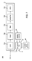
- FIG. 7 is a schematic diagram of applying the concept of the present invention to a device under test that has one single input end
- FIG. 8 is a flowchart of a correcting method according to an embodiment of the present invention.
- FIG. 2 shows a functional block diagram of a signal processing system with a built-in self-test (GIST) function according to an embodiment of the present invention.
- a signal processing system 200 includes a module under test 21 , an oscillation signal generator 22 , a translational filter 23 , and a testing module 24 .
- the signal processing system 200 may be integrated in various electronic devices, e.g., desktop computers, laptop computers, smart phones and LAN access points, or may be an independent device.
- the module under test 21 may be a signal receiving circuit.
- FIG. 3(A) shows a detailed example of a translational filter according to an embodiment of the present invention.
- the translational filter includes a mixer formed by eight metal-oxide semiconductor field-effect transistors (MOSFETs), and capacitor elements C I and C Q .
- the mixer is controlled by local oscillation signals LO IP , LO IN , LO QP and LO QN .
- the four local oscillation signals have the same frequency but different phases.
- FIG. 3(B) shows an exemplary timing diagram of the local oscillation signals.
- the capacitor elements C I and C Q located at a low-frequency side of the mixer are low-pass filters. Through effects of the mixer, the low-pass frequency resonance is translated to a bandpass frequency resonance.
- the translational filter is in overall equivalent to a bandpass filter, whose central frequency is the frequencies of the local oscillation signals LO IP , LO IN , LO QP and LO QN .
- the central frequency of the bandpass filter can be changed.
- translational filters are extensively applied in wireless communication systems and are utilized to filter and obtaining signals within a predetermined target frequency band for front-end receiving circuits.
- FIG. 4 shows a detailed example of the translational filter 23 and the testing module 24 according to an embodiment of the present invention.
- the translational filter 23 includes a mixer 23 A, and a baseband filtering circuit 23 B coupled to the low-frequency side of the mixer 23 A;
- the testing module 24 includes digital-to-analog converters (DACs) 24 A and 24 B and a controller 24 C.
- the oscillation signals LO IP , LO IN , LO QP and LO QN for controlling the mixer 23 A may be provided by the oscillation signal generator 22 .
- the controller 24 C provides a set of digital testing signal for the DACs 24 A and 24 B to correspondingly generate a set of analog testing signals. As shown in FIG.
- the DACs 24 A and 24 B are coupled to the low-frequency side of the mixer 23 A. Based on characteristics of the mixer 23 A, when the DACs 24 A and 24 B provide low-frequency analog signals at the low-frequency side of the mixer 23 A, corresponding high-frequency analog signals are generated at the high-frequency side of the mixer 23 A.
- the process is in equivalence up-converting the set of low-frequency analog signals according to the frequencies of the oscillation signals LO IP , LO IN , LO QP and LO QN .
- FIG. 5 shows a detailed example of the signal processing system 200 according to an embodiment of the present invention.
- the module under test 21 is a signal receiving circuit, has a set of differential signal input ends RFIN P and RFIN N , and includes a low-noise amplifier (LNA) 21 A, a mixer 21 B, a filter 21 C, an amplifier 21 A, and an analog-to-digital converter (ADC) 21 E.
- LNA low-noise amplifier
- ADC analog-to-digital converter
- nodes IN P and IN N at a high-frequency side of the mixer 23 A are respectively coupled to the input ends RFIN P and RFIN N of the LNA 21 A.
- the translational filter 23 plays different roles.
- the translational filter 23 When the signal processing system 200 is in a normal operation mode, the translational filter 23 provides a bandpass filtering function with the LNA 21 A to assist in filtering signals within a specific target frequency band. In contrast, when the signal processing system 200 is in a testing mode, the translational filter 23 is utilized to up-convert a testing signal generated by the testing module 24 and to thus provide the high-frequency testing signal to the input ends RFIN P and RFIN N of the LNA 21 A. That is to say, when the signal processing system 200 is in the testing mode, the oscillation signal generator 22 , the translational filter 23 , and the testing module 24 may be regarded as a testing signal generator that generates a high-frequency testing signal to a signal input end of a module under test.
- the frequency and contents of the testing signal generated by the testing module 24 may be determined according to actual requirements, and are not limited to specific patterns.
- the set of testing signals may also be DC signals.
- circuits in the testing module 24 may be adjusted according to desired testing signals, and need not necessarily include the foregoing DACs.
- the oscillation signal generator 22 may be designed in a way that the oscillation signals LO IP , LO IN , LO QP and LO QN are adjustable.
- the frequency of the testing signal provided to the module under test 21 is also adjustable.
- the oscillation signal generator 22 is an inherent element in the module under test 21 instead of being independently located outside the module under test 21 .
- the oscillation signal generator 22 may be a local oscillation signal generator in the module under test 21 .
- the oscillation signal generator 22 may not be adjustable, the frequency of the high-frequency testing signal provided by the translational filter 23 may still be adjustable through adjusting the frequency of the testing signal generated by the testing module 24 .
- the oscillation signal generator 22 and the translational filter 23 are elements originally required in the signal processing system 200 , overall costs for realizing the concept of the present invention may be far lower than those of an external testing machine capable of providing high-frequency signals.
- the concept of the present invention may be applied to various types of signal processing systems.
- the concept of the present invention is not limited to the application of a transmitting circuit in a same signal processing system, and may be further applied to a signal processing system that does not include a transmitting circuit.
- connection between the translational filter 23 and the module under test 21 may be different from that shown in FIG. 5 to perform different tests.
- the nodes IN P and IN N at the high-frequency side of the mixer 23 A may be respectively coupled to two output ends of the LNA 21 A.
- the nodes IN P and IN N at the high-frequency side of the mixer 23 A may be respectively coupled to two output ends of the amplifier 21 D.
- the connection between the baseband filtering circuit 23 B and the low-frequency side of the mixer 23 A is disconnected.
- the capacitor elements C I and C Q may be selectively separated from the connection path between the mixer 23 A and the testing module 24 , so as to prevent from affecting the testing signal transmitted from the testing module 24 to the mixer 23 A.
- the signal processing system 200 further includes a correction module 24 .
- the correction module 25 determines a correction setting for the module under test 21 .
- non-ideal factors e.g., mismatch between elements
- the above correction setting may be utilized to adjust a DC offset in the ADC 21 E.
- the correction setting generated by the correction module 25 is utilized to control the testing module 24 .
- the correction module 25 determines a correction setting for the module under test 21 .
- the correction module 25 controls the testing module 24 to provide a set of non-converted correction signals to the low-frequency side of the mixer 23 A according to the correction setting, so as to generate a set of correction signals at the high-frequency side of the mixer 23 A.
- the set of correction signals and common externally inputted signals simultaneously enter the module under test 21 .
- the set of non-converted correction signals may include a DC signal, such that the set of correction signals forwarded into the module under test 21 may compensate the non-ideal factors in the module under test 21 , e.g. eliminating the DC offset or carrier leakage.
- the correction signals that the translational filter 23 sends from the two nodes IN P and IN N may be different.
- the set correction signals may provide different correction amounts for the two differential paths. Details of the correction setting and designs of the correction signals are known to one skilled person in the art, and shall be omitted herein.
- a module under test 71 in the signal processing system 700 is similar to the module under test 21 .
- a main difference of the module under test 71 from the module under test 21 is that, a signal to be processed by an LNA 71 A, a mixer 71 B, a filter 71 C, an amplifier 71 D and an ADC 71 E is a single-ended signal instead of differential signals.
- one of the two differential input ends IN P and IN N (the input end IN N in this example) of the translational filter 23 is connected to an input end RFIN of the LNA 71 A, and the other input end (the input end IN P in this example) of the translational filter 23 is connected to ground.
- the signal provided by the testing module 24 may be up-converted by the translational filter 23 and then transmitted to the module under test 71 to be utilized for testing or correction.
- FIG. 8 shows a flowchart of the testing method.
- the translational filter includes a mixer, which has a high-frequency side and a low-frequency side.
- a testing signal is provided to the low-frequency side, so as to generate a high-frequency testing signal at the high-frequency side of the mixer.
- the high-frequency testing signal is provided to a signal input end of a module under test.
- the translational filter provides the module under test with a filtering function.
- a signal processing system with a BIST function and a testing method thereof are disclosed by the present invention.
- a translational filter that generates a testing signal in a chip overall testing costs can be significantly lowered.
- the testing method of the present invention is also applicable to a signal processing system that does not include a transmitting circuit.
Landscapes
- Physics & Mathematics (AREA)
- Engineering & Computer Science (AREA)
- General Engineering & Computer Science (AREA)
- General Physics & Mathematics (AREA)
- Electromagnetism (AREA)
- Computer Networks & Wireless Communication (AREA)
- Signal Processing (AREA)
- Tests Of Electronic Circuits (AREA)
- Monitoring And Testing Of Transmission In General (AREA)
Abstract
Description
Claims (19)
Applications Claiming Priority (3)
| Application Number | Priority Date | Filing Date | Title |
|---|---|---|---|
| TW102120298A TWI517605B (en) | 2013-06-07 | 2013-06-07 | Signal processing system with built-in self-test function, test method thereof and test signal generator |
| TW102120298 | 2013-06-07 | ||
| TW102120298A | 2013-06-07 |
Publications (2)
| Publication Number | Publication Date |
|---|---|
| US20140365841A1 US20140365841A1 (en) | 2014-12-11 |
| US9429620B2 true US9429620B2 (en) | 2016-08-30 |
Family
ID=52006550
Family Applications (1)
| Application Number | Title | Priority Date | Filing Date |
|---|---|---|---|
| US14/273,985 Active 2034-09-23 US9429620B2 (en) | 2013-06-07 | 2014-05-09 | Signal processing system with BIST function, testing method thereof and testing signal generator |
Country Status (2)
| Country | Link |
|---|---|
| US (1) | US9429620B2 (en) |
| TW (1) | TWI517605B (en) |
Families Citing this family (2)
| Publication number | Priority date | Publication date | Assignee | Title |
|---|---|---|---|---|
| EP3286833B1 (en) * | 2015-04-24 | 2020-11-18 | u-blox AG | Method and apparatus for mixing signals using charge canceller circuit |
| US10284236B1 (en) * | 2018-05-03 | 2019-05-07 | Infineon Technologies Ag | Multi channel self-test for RF devices |
Citations (11)
| Publication number | Priority date | Publication date | Assignee | Title |
|---|---|---|---|---|
| US6449307B1 (en) * | 1998-06-05 | 2002-09-10 | Murata Manufacturing Co., Ltd. | Apparatus for measuring electrical characteristics of circuit |
| US6498929B1 (en) * | 1996-06-21 | 2002-12-24 | Kabushiki Kaisha Toshiba | Receiver having DC offset decreasing function and communication system using the same |
| US20040148580A1 (en) * | 2003-01-17 | 2004-07-29 | Texas Instruments Incorporated | On-chip receiver sensitivity test mechanism |
| US20050107059A1 (en) * | 2001-06-20 | 2005-05-19 | Heinz Lehning | Compensation of mismatch between quadrature paths |
| US20060026476A1 (en) * | 2004-07-29 | 2006-02-02 | Nec Electronics Corporation | Integrated circuit device and testing device |
| US20070060069A1 (en) * | 2005-09-15 | 2007-03-15 | Silicon Laboratories Inc. | System and method for reducing spurious emissions in a wireless communication device including a testing apparatus |
| US20080103719A1 (en) * | 2006-10-26 | 2008-05-01 | Samsung Electronics Co., Ltd | Method of generating test clock signal and test clock signal generator for testing semiconductor devices |
| US20100177811A1 (en) * | 2009-01-13 | 2010-07-15 | Infineon Technologies Ag | Integrated Transceiver Loop Back Self Test by Amplitude Modulation |
| US20120126821A1 (en) * | 2010-11-23 | 2012-05-24 | Hans-Peter Forstner | System and Method for Testing a Radio Frequency Integrated Circuit |
| US20130107918A1 (en) * | 2011-11-01 | 2013-05-02 | Renesas Electronics Corporation | High-frequency signal processor and wireless communication system |
| US20140355655A1 (en) * | 2013-06-03 | 2014-12-04 | Texas Instruments Incorporated | Built in self test and method for rf transceiver systems |
-
2013
- 2013-06-07 TW TW102120298A patent/TWI517605B/en not_active IP Right Cessation
-
2014
- 2014-05-09 US US14/273,985 patent/US9429620B2/en active Active
Patent Citations (12)
| Publication number | Priority date | Publication date | Assignee | Title |
|---|---|---|---|---|
| US6498929B1 (en) * | 1996-06-21 | 2002-12-24 | Kabushiki Kaisha Toshiba | Receiver having DC offset decreasing function and communication system using the same |
| US6449307B1 (en) * | 1998-06-05 | 2002-09-10 | Murata Manufacturing Co., Ltd. | Apparatus for measuring electrical characteristics of circuit |
| US20050107059A1 (en) * | 2001-06-20 | 2005-05-19 | Heinz Lehning | Compensation of mismatch between quadrature paths |
| US20040148580A1 (en) * | 2003-01-17 | 2004-07-29 | Texas Instruments Incorporated | On-chip receiver sensitivity test mechanism |
| US20060026476A1 (en) * | 2004-07-29 | 2006-02-02 | Nec Electronics Corporation | Integrated circuit device and testing device |
| US20070060069A1 (en) * | 2005-09-15 | 2007-03-15 | Silicon Laboratories Inc. | System and method for reducing spurious emissions in a wireless communication device including a testing apparatus |
| US20080103719A1 (en) * | 2006-10-26 | 2008-05-01 | Samsung Electronics Co., Ltd | Method of generating test clock signal and test clock signal generator for testing semiconductor devices |
| US20100177811A1 (en) * | 2009-01-13 | 2010-07-15 | Infineon Technologies Ag | Integrated Transceiver Loop Back Self Test by Amplitude Modulation |
| US20120126821A1 (en) * | 2010-11-23 | 2012-05-24 | Hans-Peter Forstner | System and Method for Testing a Radio Frequency Integrated Circuit |
| US20130107918A1 (en) * | 2011-11-01 | 2013-05-02 | Renesas Electronics Corporation | High-frequency signal processor and wireless communication system |
| US20140355655A1 (en) * | 2013-06-03 | 2014-12-04 | Texas Instruments Incorporated | Built in self test and method for rf transceiver systems |
| US9136899B2 (en) * | 2013-06-03 | 2015-09-15 | Texas Instruments Incorporated | Built in self test and method for RF transceiver systems |
Also Published As
| Publication number | Publication date |
|---|---|
| TW201448498A (en) | 2014-12-16 |
| TWI517605B (en) | 2016-01-11 |
| US20140365841A1 (en) | 2014-12-11 |
Similar Documents
| Publication | Publication Date | Title |
|---|---|---|
| KR101739921B1 (en) | Offset compensation in a receiver | |
| US9300444B2 (en) | Wideband quadrature error correction | |
| US11012104B2 (en) | Apparatus and methods for calibrating radio frequency transmitters to compensate for common mode local oscillator leakage | |
| KR102492442B1 (en) | Method and apparatus to detect lo leakage and image rejection using a single transistor | |
| US9871504B2 (en) | Differential phase adjustment of clock input signals | |
| US20140162568A1 (en) | On-chip calibration and built-in-self-test for soc millimeter-wave integrated digital radio and modem | |
| RU2450421C2 (en) | Correction of shift for passive mixers | |
| US8744385B2 (en) | Efficient reduction of local oscillator leakage | |
| US8718576B2 (en) | Radio frequency modulator and method thereof | |
| CN107257947B (en) | Transmit digital-to-analog converter (DAC) spurious attenuation | |
| KR20110091027A (en) | Duty Cycle Adjustment for Local Oscillator Signals | |
| US8112055B2 (en) | Calibrating receive chain to reduce second order intermodulation distortion | |
| TWI811577B (en) | Detector circuit and method for detecting local oscillator leakage and image tone | |
| US9509419B2 (en) | Communication circuit and associated calibration method | |
| CN111480300A (en) | Local oscillator leakage detection and cancellation | |
| TWI813032B (en) | Bias arrangements | |
| US9429620B2 (en) | Signal processing system with BIST function, testing method thereof and testing signal generator | |
| CN112825487A (en) | Radio frequency receiving link and radio frequency transmitting and receiving device | |
| CN104242969B (en) | Signal processing system, its test method and test signal generator | |
| US12355474B2 (en) | Enhanced DPD method to correct gain flatness for wireless communications systems | |
| CN113839622A (en) | Transconductance circuit with programmable trade-off between bandwidth and flicker noise | |
| US20250096839A1 (en) | Oscillator Leakage Calibration | |
| US11588612B2 (en) | Communication chip | |
| US12015417B2 (en) | Input buffer circuit, analog-to-digital converter system, receiver, base station, mobile device and method for operating an input buffer circuit | |
| CN120226261A (en) | Oscillator feedthrough calibration |
Legal Events
| Date | Code | Title | Description |
|---|---|---|---|
| AS | Assignment |
Owner name: MSTAR SEMICONDUCTOR, INC., TAIWAN Free format text: ASSIGNMENT OF ASSIGNORS INTEREST;ASSIGNORS:YEN, SHIH-CHIEH;HUNG, CHIH-MING;SIGNING DATES FROM 20140428 TO 20140429;REEL/FRAME:032867/0341 |
|
| STCF | Information on status: patent grant |
Free format text: PATENTED CASE |
|
| FEPP | Fee payment procedure |
Free format text: MAINTENANCE FEE REMINDER MAILED (ORIGINAL EVENT CODE: REM.); ENTITY STATUS OF PATENT OWNER: LARGE ENTITY |
|
| AS | Assignment |
Owner name: MEDIATEK INC., TAIWAN Free format text: MERGER;ASSIGNOR:MSTAR SEMICONDUCTOR, INC.;REEL/FRAME:052931/0468 Effective date: 20190115 |
|
| FEPP | Fee payment procedure |
Free format text: SURCHARGE FOR LATE PAYMENT, LARGE ENTITY (ORIGINAL EVENT CODE: M1554); ENTITY STATUS OF PATENT OWNER: LARGE ENTITY |
|
| MAFP | Maintenance fee payment |
Free format text: PAYMENT OF MAINTENANCE FEE, 4TH YEAR, LARGE ENTITY (ORIGINAL EVENT CODE: M1551); ENTITY STATUS OF PATENT OWNER: LARGE ENTITY Year of fee payment: 4 |
|
| MAFP | Maintenance fee payment |
Free format text: PAYMENT OF MAINTENANCE FEE, 8TH YEAR, LARGE ENTITY (ORIGINAL EVENT CODE: M1552); ENTITY STATUS OF PATENT OWNER: LARGE ENTITY Year of fee payment: 8 |