US9417517B2 - Photomask having a blind region including periodical clear portions - Google Patents
Photomask having a blind region including periodical clear portions Download PDFInfo
- Publication number
- US9417517B2 US9417517B2 US14/300,416 US201414300416A US9417517B2 US 9417517 B2 US9417517 B2 US 9417517B2 US 201414300416 A US201414300416 A US 201414300416A US 9417517 B2 US9417517 B2 US 9417517B2
- Authority
- US
- United States
- Prior art keywords
- region
- dark
- photo mask
- reticle
- mask according
- Prior art date
- Legal status (The legal status is an assumption and is not a legal conclusion. Google has not performed a legal analysis and makes no representation as to the accuracy of the status listed.)
- Active, expires
Links
Images


Classifications
-
- G—PHYSICS
- G03—PHOTOGRAPHY; CINEMATOGRAPHY; ANALOGOUS TECHNIQUES USING WAVES OTHER THAN OPTICAL WAVES; ELECTROGRAPHY; HOLOGRAPHY
- G03F—PHOTOMECHANICAL PRODUCTION OF TEXTURED OR PATTERNED SURFACES, e.g. FOR PRINTING, FOR PROCESSING OF SEMICONDUCTOR DEVICES; MATERIALS THEREFOR; ORIGINALS THEREFOR; APPARATUS SPECIALLY ADAPTED THEREFOR
- G03F1/00—Originals for photomechanical production of textured or patterned surfaces, e.g., masks, photo-masks, reticles; Mask blanks or pellicles therefor; Containers specially adapted therefor; Preparation thereof
- G03F1/38—Masks having auxiliary features, e.g. special coatings or marks for alignment or testing; Preparation thereof
-
- G—PHYSICS
- G03—PHOTOGRAPHY; CINEMATOGRAPHY; ANALOGOUS TECHNIQUES USING WAVES OTHER THAN OPTICAL WAVES; ELECTROGRAPHY; HOLOGRAPHY
- G03F—PHOTOMECHANICAL PRODUCTION OF TEXTURED OR PATTERNED SURFACES, e.g. FOR PRINTING, FOR PROCESSING OF SEMICONDUCTOR DEVICES; MATERIALS THEREFOR; ORIGINALS THEREFOR; APPARATUS SPECIALLY ADAPTED THEREFOR
- G03F1/00—Originals for photomechanical production of textured or patterned surfaces, e.g., masks, photo-masks, reticles; Mask blanks or pellicles therefor; Containers specially adapted therefor; Preparation thereof
- G03F1/50—Mask blanks not covered by G03F1/20 - G03F1/34; Preparation thereof
Definitions
- the present invention relates to a lithography photo mask for use in manufacturing a semiconductor device.
- the photo mask (the reticle) comprises a mask substrate (a reticle substrate) composed of a transparent substrate, and a dark film (a dark portion) which is provided on the mask substrate (the reticle substrate) and which has either a function for shielding light or a function for passing through the light partially.
- Absorption energy from a radiation beam during exposure heats the photo mask (the reticle) to make the photo mask (the reticle) expand.
- Patent Literature 1 discloses a correction method comprising: calculating thermal expansion of a photo mask (a reticle) using a model calculation; and correcting it using a high-order correction technique.
- Patent Literature 1 corrects the thermal expansion of the reticle using the high-order correction technique
- the correction method merely corrects fluctuations of the shape of a complicated reticle due to the thermal expansion approximately using a different overlap correction technique such as a scanning rate adjustment. Therefore, the correction method disclosed in Patent Literature 1 cannot perfectly correct the thermal expansion of the reticle (residues persist).
- Non Patent Literature 1 temperature control technology of a photo mask (a reticle) is disclosed in article which is contributed by J. Mulkens et al. to Proc. of SPIE Vol. 8326 (2012), pages 12-14, and which has a title of “Driving Imaging and Overlay Performance to the Limits with Advanced Lithography Optimization” (which will later be called “Non Patent Literature 1”).
- Non Patent Literature 1 merely discloses the temperature control technology of the photo mask (the reticle).
- JP-A-2012-22036 (which corresponds to US 2012/0009510 A1 and which will later be called “Patent Literature 2”) discloses a lithography mask.
- the lithography mask disclosed in Patent Literature 2 is composed of a transparent substrate and a light blocking film or a dark film.
- the light blocking film (the dark film) includes a first patterning region and a second patterning region located adjacent to the first patterning region.
- the first patterning region corresponds to a sizable unpatterned region of a resist film
- the second patterning region corresponds to a patterned region of the resist film.
- the present invention seeks to solve one or more of the above problems, or to improve upon those problems at least in part.
- a photo mask comprising: a plurality of dark patterns disposed on a transparent substrate; a first region including the dark patterns that are disposed with a wider space than a first distance; a shield region, adjacent to the first region on the transparent substrate, being filled with the dark pattern; and a second region, faced to the first region across the shield region, including the dark patterns that are disposed with a narrow space than a second distance, wherein the second distance is narrower than ninety percent of the first distance.
- a photo mask comprising: a transparent substrate including first, second, and third regions, the third region adjacent to the first region, the first and the second regions facing each other across the third region; first dark patterns that are arranged with a first pitch in the first region; second dark patterns that are arranged with a second pitch in the second region; and a third dark pattern filling in the third region, wherein the second pitch is narrower than ninety percent of the first pitch.
- a photo mask comprising: a first region including a plurality of first clear portions having a minimum size; a dark region surrounding the first region; and a second region surrounding the dark region and including a plurality of second clear portions having a maximum size that is smaller than ninety percent of at least the minimum size.
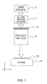
- FIG. 1 is a schematic construction view illustrating an exposure apparatus in which a photo mask (a reticle) to which the present invention is applied is mounted;
- FIG. 2 is a plan view illustrating the photo mask (the reticle) shown in FIG. 1 ;
- FIG. 3 is an enlarged plan view illustrating a detailed configuration of a reticle in a first related art
- FIG. 4 is an enlarged plan view illustrating a detailed configuration of a reticle in a second related art
- FIG. 5 is an enlarged plan view illustrating by enlarging a part of a reticle in a third related art
- FIG. 6 is an enlarged plan view illustrating by enlarging a part of a reticle in a fourth related art
- FIG. 7 is an enlarged plan view illustrating a detailed configuration of a reticle according to a first exemplary embodiment of this invention.
- FIG. 8 is an enlarged plan view illustrating a detailed configuration of a reticle according to a second exemplary embodiment of this invention.
- FIG. 9 is an enlarged plan view illustrating a reticle according to a first example of this invention, by enlarging a region 48 circled in FIG. 7 ;
- FIG. 10 is a graph for use in describing an effect of the reticle according to the first example illustrated in FIG. 9 , in contradistinction to the reticle in the fourth related art illustrated in FIG. 6 ;
- FIG. 11 is an enlarged plan view illustrating a reticle according to a second example of this invention, by enlarging a region 48 circled in FIG. 7 ;
- FIG. 12 is an enlarged plan view illustrating a reticle according to a third example of this invention, by enlarging a region 48 circled in FIG. 7 ;
- FIG. 13 is a block diagram illustrating a configuration of a mask data preparing apparatus according to an exemplary embodiment of this invention.
- the description will proceed to a layout of respective components by setting a coordinate system of xyz.
- the z direction is a direction orthogonal to a surface of a wafer
- the x direction is a direction orthogonal to the z direction in a plane parallel to the surface of the wafer
- the y direction is a direction orthogonal to the x direction in the plane parallel to the surface of the wafer.
- the y direction is referred to as a first direction
- the x direction is referred to as a second direction
- the z direction is referred to as a third direction.
- FIG. 1 is a schematic construction view illustrating an exposure apparatus in which a photo mask (a reticle) to which the present invention is applied is mounted.
- the exposure apparatus comprises a light source 2 , an illumination system 4 , a projecting lens 6 , and a stage 8 .
- a photo mask 10 is disposed between the illumination system 4 and the projecting lens 6 .
- a wafer 20 to which a photoresist (a photosensitive organic film) is applied is disposed on an upper surface of the stage 8 .
- the light source 2 comprises an ArF excimer laser (a designed wavelength of light: 193 nm).
- the illumination system 4 comprises, as an aperture plate (not shown), an aperture portion for a cross-pole illumination.
- the exposure apparatus may comprise a limmersion exposure apparatus (numerical aperture NA: 0.92) including the ArF excimer laser.
- the photo mask 10 is called as a “reticle” used in a reduced projection exposure.
- a size (a dimension) of a pattern formed in the photo mask (the reticle) 10 is reduced to a quarter or (1 ⁇ 4) and is transferred to the photoresist (the photosensitive organic film) on the wafer 20 . That is, a transferring factor is equal to a quarter or (1 ⁇ 4).
- a desired dark pattern is disposed in the photo mask (the reticle) 10 .
- the wafer 20 is also called a semiconductor substrate.
- a semiconductor device is generally manufactured in the manner as follows.
- a work layer (not shown) is formed on the semiconductor substrate 20 .
- a photoresist (a photosensitive organic film) is formed on the work layer.
- the photosensitive organic film on the semiconductor substrate 20 is exposed by using, as a mask, a photo mask 10 in which a desired dark pattern is disposed.
- the exposed photosensitive organic film is developed to form a first pattern where a part of the photosensitive organic film is selectively removed.
- the above-mentioned work layer is selectively removed by using the first pattern as a mask.
- FIG. 2 is a plan view illustrating the reticle 10 inserted on exposure.
- the description will proceed on the assumption that the illustrated reticule 10 comprises a binary mask and the photoresist (the photosensitive organic film) applied to the wafer 20 ( FIG. 1 ) is a positive type.
- the reticle 10 comprises a reticle substrate 30 , a rectangular ring-shaped dark band 32 , and a rectangular exposure region 34 .
- the reticle substrate 30 comprises a transparent substrate such as a glass or the like.
- the dark band 32 is provided on a lower surface of the reticle substrate 30 and is made of, for example, chrome (Cr).
- the rectangular exposure region 34 is formed in the dark band 32 . In other words, the rectangular exposure region 34 is enclosed with the dark band 32 .
- the exposure region 34 has a rectangular shape which is long in the y direction (the first direction).
- the reticle substrate 30 is also called a mask substrate.
- FIG. 3 is an enlarged plan view illustrating a detailed configuration of the photo mask (the reticle) 10 (the rectangular exposure region 34 enclosed with the dark band 32 ) in a first related art.
- the exposure region 34 comprises a plurality of circuit formation regions 40 and a dark region 42 .
- the plurality of circuit formation regions 40 are disposed at regular intervals in length and width directions (in the y direction and the x direction) in a matrix fashion.
- the dark region 42 is disposed around each of the plurality of circuit formation region 40 . That is, each circuit formation region 40 is enclosed with the dark region 42 .
- the plurality of circuit formation regions 40 are disposed so as to be symmetric with respect to a central point O of the reticle substrate 30 ( FIG. 2 ).
- each circuit formation region 40 has a rectangular shape.
- Each circuit formation region 40 is also called a first region while the dark region is also called a second region.
- a radiation beam is irradiated to the reticle (the photo mask) 10 including the exposure region 34 according to the first related art during exposure.
- the dark band 32 and the rectangular exposure region 34 enclosed therewith expand uniformly in the length and width directions (the y direction and the x direction) up to a rectangular region 44 depicted at a broken line of FIG. 3 .
- the rectangular region 44 depicted at the broken line is an enlarged amount of the reticle substrate.
- the reason why the reticle substrate 30 expands uniformly in the length and width directions is that the plurality of circuit formation regions 40 are disposed so as to be symmetric with respect to the central point O.
- FIG. 4 is an enlarged plan view illustrating a detailed configuration of the photo mask (the reticle) 10 (the rectangular exposure region 34 enclosed with the dark band 32 ) in a second related art.
- the photo mask (the reticle) 10 of the second related art is similar in structure to the photo mask (the reticle) 10 of the first related art illustrated in FIG. 3 except that the exposure region 34 is modified from that illustrated in FIG. 3 as will later become clear.
- the exposure region 34 in the photo mask (the reticle) 10 of the second related art includes a dark portion 42 a having a large area at a lower portion thereof.
- a radiation beam is irradiated to the reticle (the photo mask) 10 including the exposure region 34 according to the second related art during exposure.
- the dark band 32 and the rectangular exposure region 34 enclosed therewith expand up to a rectangular region 44 depicted at a broken line of FIG. 4 .
- the lower portion of the exposure region 34 expands by a larger amount in comparison with other portions. This is because, inasmuch as the exposure region 34 includes the dark portion 42 a having the large area at the lower portion thereof, the radiation beam is absorbed in the dark portion 42 a having the large area to generate heat more than the other portions. Accordingly, the reticule substrate 30 ( FIG. 2 ) expands at a lower portion thereof up to a maximum portion 44 a of the enlarged amount of the reticle substrate.
- the amount of absorption heating is biased and the alignment accuracy becomes worse due to a biased expansion of the reticle substrate 30 ( FIG. 2 ).
- FIG. 5 is an enlarged plan view illustrating by enlarging a part (a boundary portion between a circuit formation region (a first region) 41 and a dark region (a second region) 43 ) of a photo mask (a reticle) in a third related art.
- a plurality of first dark patterns 60 are arranged in the circuit formation region (the first region) 41 at a first distance 50 .
- the whole area of the dark region (the second region) 42 is covered with a second dark pattern 64 .
- FIG. 6 is an enlarged plan view illustrating by enlarging a part (a boundary portion between a circuit formation region (a first region) 41 and a dark region (a second region) 43 ) of a photo mask (a reticle) in a fourth related art.
- the photo mask (the reticle) of the fourth related art corresponds to the lithography mask disposed in the above-mentioned Patent Literature 2.
- a plurality of first dark patterns 60 are arranged in the circuit formation region (the first region) 41 at a first distance 50 (at a first pitch dc) in the manner as the photo mask (the reticle) of the above-mentioned third related art.
- a plurality of second dark patterns 64 are arranged in the dark region (the second region) 43 at a second distance (at a second pitch dn).
- the second distance 55 (the second pitch dn) is narrower than the first distance 50 (the first pitch dc).
- each of the plurality of second dark patterns 64 has a line shape of a first width w extending in the y direction (the first direction) and the plurality of second dark patterns 64 are periodically arranged at the second distance 55 (the second pitch dn) in the x direction (the second direction) intersecting the y direction (the first direction).
- the pattern formed in the dark region (the second region) 43 is called a “non-resolution dummy pattern”.
- the pattern formed in the circuit formation region (the first region) 41 is called a “resolution pattern”.
- circuit formation region (the first region) 41 corresponds to “the second patterning region” of the above-mentioned Patent Literature 2 while the dark region (the second region) 43 corresponds to “the first patterning region” of the above-mentioned Patent Literature 2.
- FIG. 7 is an enlarged plan view illustrating a detailed configuration of a photo mask (a reticle) (a rectangular exposure region 34 enclosed with a dark band 32 ) according to a first exemplary embodiment of this invention.
- the exposure region 34 of the photo mask (the reticle) comprises a plurality of circuit formation regions 41 , a dark region 43 , and a plurality of dark portions 46 .
- the plurality of circuit formation regions 41 are disposed at regular intervals in length and width directions (the y direction and the x direction) in a matrix fashion.
- the dark portion region 43 is disposed apart from the plurality of circuit formation regions 41 .
- the plurality of dark portions 46 are disposed between the plurality of circuit formation regions 41 and the dark region 43 so as to enclose each circuit formation region 41 . That is, each circuit formation region 41 is enclosed with the dark portion 46 . In other words, the dark portion 46 is adjacent to the circuit formation region 41 .
- each circuit formation region 41 has a rectangular shape.
- Each dark portion 46 enclosing the circuit formation region 41 has a rectangular ring shape.
- the circuit formation region 41 is also called a first region
- the dark region 43 is also called a second region
- the dark portion 46 is also called a shield region.
- the dark portion (the shield region) 46 is also called a third region or a dark region.
- the exposure region 34 of the photo mask (the reticle) of the first related art illustrated in FIG. 3 differs from it in a way where the dark portions (the shield regions) 46 are provided at boundaries between the circuit formation regions (the first regions) 41 and the dark region (the second region) 43 .
- FIG. 9 is an enlarged plan view of a portion of a region 48 circled in FIG. 7 , by enlarging it.
- a plurality of dark patterns 60 , 62 , and 64 are disposed on the transparent substrate 30 .
- the dark patterns 60 are disposed with a wider space than the first distance 50 .
- the whole area of the dark portion (the shield region) 46 is covered with the dark pattern 62 .
- the dark patterns 64 are disposed with a narrower space than the second distance 55 .
- the dark region (the second region) 43 is opposed to the circuit formation region (the first region) 41 with the dark portion (the shield region) 46 sandwiched therebetween.
- the second distance 55 is narrower than ninety present of the first distance 50 .
- the photo mask ( 10 ) comprises: the plurality of dark patterns ( 60 , 62 , 64 ) disposed on the transparent substrate ( 30 ), the first, the shield, and the second regions ( 41 , 46 , 43 ) disposed on the transparent substrate ( 30 ), wherein the first region ( 41 ) includes the dark patterns ( 60 ) that are disposed with the wider space than the first distance ( 50 ), the shield region ( 46 ) is adjacent to the first region ( 41 ) and is filled with the dark pattern ( 62 ), the second region ( 43 ) is faced to the first region ( 41 ) across the shield region ( 46 ) and includes the dark patterns ( 64 ) that are disposed with the narrower space than the second distance ( 55 ), and wherein the second distance ( 55 ) is narrower than ninety percent of the first distance ( 50 ).
- the pattern formed in the circuit formation region (the first region) 41 is called the “resolution pattern” while the pattern formed in the dark region (the second region) 43 is called the “non-resolution dummy pattern.”
- the pattern formed in the dark portion (the shield region) 46 is called a “dark pattern.”
- a radiation beam is irradiated to the reticle (the photo mask) 10 including the exposure region 34 according to the first exemplary embodiment during exposure.
- the dark band 32 and the rectangular exposure region 34 enclosed therewith expand uniformly in the length and width directions (the y direction and the x direction) up to a rectangular region 45 depicted at a broken line of FIG. 7 .
- the rectangular region 45 depicted at the broken line is an enlarged amount of the reticle substrate.
- the reason why the reticle substrate 30 expands uniformly in the length and width directions is that the plurality of circuit formation regions 41 are disposed so as to be symmetric with respect to the central point O.
- the enlarged amount 45 of the reticle substrate is remarkably less than the enlarged amount 44 of the reticle substrate. This is because, inasmuch as the non-resolution dummy pattern is formed in the dark region (the second region) 43 , it is possible to suppress the thermal expansion of the reticle substrate 30 due to the above-mentioned absorption heating of the radiation beam.
- the photo mask 10 it is possible to prevent a detrimental effect due to the above-mentioned optical proximity in the photo mask (the reticle) 10 .
- FIG. 8 is an enlarged plan view illustrating a detailed configuration of a photo mask (a reticle) 10 (a rectangular exposure region 34 enclosed with a dark band 32 ) according to a second exemplary embodiment of this invention.
- the photo mask (the reticle) 10 of the second exemplary embodiment is similar in structure to the photo mask (the reticle) 10 of the first exemplary embodiment illustrated in FIG. 7 except that the exposure region 34 is modified from that illustrated in FIG. 7 as will later become clear.
- the exposure region 43 in the photo mask (the reticle) 10 of the second exemplary embodiment includes a dark portion 43 a having a large area at a lower portion thereof.
- a radiation beam is irradiated to the reticle (the photo mask) 10 including the exposure region 34 according to the second exemplary embodiment during exposure.
- the dark band 32 and the rectangular exposure region 34 enclosed therewith expand uniformly in the length and width directions (the y direction and the x direction) up to a rectangular region 45 depicted at a broken line of FIG. 8 .
- the photo mask 10 according to the second exemplary embodiment also, it is possible to prevent a detrimental effect due to the above-mentioned optical proximity.
- FIG. 9 is the enlarged plan view illustrating the reticle according to the first example of this invention, by enlarging the region 48 (i.e. a boundary portion of the first region, the second region, and the third region) circled in FIG. 7
- the reticle according to the first example comprises a transparent substrate 30 which includes a circuit formation region (a first region) 41 , a dark region (a second region) 43 , and a dark portion (a third region) 46 surrounding the circuit formation region (the first region) 41 .
- the dark portion (the third region) 46 is adjacent to the circuit formation region (the first region) 41 .
- the dark region (the second region) 43 is faced to the circuit formation region (the first region) 41 across the dark portion (the third region) 46 .
- the dark portion (the third region) 46 is also called a dark region.
- the reticle according to the first example comprises first dark patterns 60 each having a line shape, second dark patterns 64 each having a line shape, and a third dark pattern 62 .
- the first dark patterns are arranged with a first pitch dc in the circuit formation region (the first region) 41 .
- the second dark patterns 64 are arranged with a second pitch dn in the dark region (the second region) 43 .
- the third dark pattern 62 fills in the dark portion (the third region) 46 as a whole.
- the second pitch dn is narrower the ninety percent of the first pitch dc.
- the reticle or the photo mask ( 10 ) comprises: the transparent substrate ( 30 ) including the first, the second and the third regions ( 41 , 43 , 46 ), the third region ( 46 ) adjacent to the first region ( 41 ), the first and the second regions ( 41 , 43 ) facing each other across the third region ( 46 ); the first dark patterns ( 60 ) having the line shape that are arranged with the first pitch (dc) in the first region ( 41 ); the second dark patterns ( 64 ) having the line shape that arranged with the second pitch (dn) in the second region ( 43 ); and the third dark pattern ( 62 ) filling in the third region ( 46 ), wherein the second pitch (dn) is narrower than ninety percent of the first pitch (dc).
- the photo mask ( 10 ) comprises: the first region ( 41 ) including first cleat portions having a minimum size; the dark region ( 46 ) surrounding the first region ( 41 ); and the second region ( 43 ) surrounding the dark region ( 46 ) and including second clear portions having a maximum size that is smaller than ninety present of at least the minimum size.
- each of the first dark patterns 60 , the second dark patterns 64 , and the third dark pattern 62 has an equal transmittance for an designed wavelength ⁇ of light that is less than ten percent.
- each second dark pattern 64 has a line shape extending in the y direction (the first direction) with the first width w, and the second dark patterns 64 are arranged periodically at the second distance 55 (the second pitch dn) in the x direction (the second direction) that intersects the y direction (the first direction).
- a non-resolution dummy pattern with the second pitch dn exceeding resolution limitations of lithography is arranged as the non-resolution dummy pattern formed in the dark region (the second region) 43 , and it is therefore possible to put a larger non-resolution dummy pattern in the dark region (the second region) 43 without causing the photoresist (the photosensitive organic film) on the wafer 20 ( FIG. 1 ) to resolve an unnecessary pattern.
- exposure condition has the designed wavelength ⁇ of light in the light source 2 ( FIG. 1 ), a numerical aperture NA of the wafer 20 ( FIG. 1 ) side, a coherent factor ⁇ ( ⁇ out , ⁇ in ) of illumination, and a transferred factor M.
- the second pitch dn of the 424 nm in the dark region (the second region) 42 corresponds to a pitch of 106 nm on the wafer 20 ( FIG. 1 ) because the pitch is reduced to (1 ⁇ 4).
- the first pitch dc of the resolution pattern formed in the circuit formation region (the first region) 41 is set to 498 nm.
- the first pitch dc corresponds to a pitch of 124.5 nm on the wafer 20 ( FIG. 1 ).
- the pitch ratio of (the non-resolution dummy pattern)/(the resolution pattern) is equal to 0.85-fold.
- the second pitch dn calculated by the above-mentioned Rayleigh's equation has a lower limit equal to 441.6 nm
- the above-mentioned pitch ratio is actually less than 0.887. Therefore, in the first example, due to rounding, the second pitch dn is set to be narrower than ninety percent of the first pitch dc.
- a method of manufacturing a semiconductor device comprises: forming a work layer on the semiconductor substrate ( 20 ); forming the photosensitive organic film on the work layer; exposing the photosensitive organic film on the semiconductor substrate ( 20 ) using, as a mask, the photo mask ( 10 ) in which the desired dark patterns ( 60 , 62 , 64 ) are arranged; developing the exposed photosensitive organic film to form a first pattern in which part of the photosensitive organic film is selectively removed; and selectively removing the work layer using the first pattern as a mask, wherein the photo mask ( 10 ) comprises the first through the third regions ( 41 , 43 , 46 ), the dark patterns ( 60 ) are arranged in the first region ( 41 ) with a wider distance ( 50 ) where the pattern is transferred to the photosensitive organic film, the third region ( 46 ) surrounds the first region ( 41 ) and is covered with the dark pattern ( 62 ) as a whole, the dark patterns ( 64 ) are arranged in the second region ( 46 ) with
- the ratio of a width dimension of a line to a width dimension of a space is equal to 1:1.
- the first distance 50 is equal to 249 nm while the second distance 55 is equal to 212 nm. Accordingly, the second distance 55 is narrower than ninety percent of the first distance 50 .
- the second distance 55 is 0.5-fold of the second pitch dn in the first example.
- the first width (size) w of each second dark pattern 64 is calculated by changing the second distance (slit size) 55 of the reticle 10 with the second pitch dn calculated by the above-mentioned Rayleigh's equation, and making the second distance (the slit size) 55 of the largest slit size within a range where decline does not occur in the photoresist (the photosensitive organic film) a manufacturing condition of the non-resolution dummy pattern.
- the first width (the size) of each second dark pattern 64 was determined to 188 nm.
- the second distance (the slit size) 55 may range from forty present to sixty percent of the pitch (the second pitch dn) of the second dark pattern 64 which is defined as the sum of the first width w and the second distance 55 .
- a distance D is calculated as follows.
- the distance D is a distance between the circuit formation region (the first region) 41 and the dark region (the second region) 43 which face each other across the dark portion (the shield region) 46 .
- the distance D is changed to calculate a distance so as to have little effect on the circuit formation region (the first region) 41 and so that the non-resolution dummy pattern is not arranged within this region.
- This distance D was calculated using a lithography simulator under the above-mentioned exposure condition and the condition of the above-mentioned Rayleigh's equation. As a result, four micrometers was obtained as the distance D.
- the distance D may be not less than four micrometers.
- the distance D was set so as to range from four micrometers to twenty micrometer.
- the reticle substrate (the mask substrate) 30 ( FIG. 2 ) is made of a material of quartz which has a transmittance to the designed wavelength ⁇ of light more than eighty-five percent.
- the reticle having structure of FIG. 9 that is formed in the manner as described above was made a product and twenty-five wafers was continuously exposed by using the exposure apparatus illustrated in FIG. 1 .
- the present inventor confirmed that the non-resolution dummy pattern arranged in the dark region (the second region) 43 does not form unnecessary resist pattern to the semiconductor manufacture.
- the reticle having structure of FIG. 6 also was made a product and twenty-five wafers were continuously exposed.
- FIG. 10 is a graph showing those results.
- the abscissa represents number of wafers 20 and the ordinate represents reticle magnification [ppm].
- a solid line represents the results (after measures) in a case of using the reticle having the structure of FIG. 9 while a broken line represents the results (before measures) in a case of using the reticle having the structure of FIG. 6 .
- FIG. 11 is the enlarged plan view illustrating the reticle according to the second example of this invention, by enlarging the region 48 (i.e. a boundary portion of the first region, the second region, and the third region) circled in FIG. 7 .
- region 48 i.e. a boundary portion of the first region, the second region, and the third region
- the reticle according to the second example comprises a transparent substrate 30 which includes a circuit formation region (a first region) 41 , a dark region (a second region) 43 , and a dark portion (a shied region or a third region) 46 surrounding the circuit formation region (the first region) 41 .
- the dark portion (the shield region or the third region) 46 is adjacent to the circuit formation region (the first region) 41 .
- the dark region (the second region) 43 is faced to the circuit formation region (the first region) 41 across the dark portion (the shield region or the third region) 46 .
- the reticle according to the second example is similar in structure to the reticle according to the first example illustrated in FIG. 9 except that the resolution pattern formed in the circuit formation region (the first region) 41 is modified from that illustrated in FIG. 9 as will later become clear.
- the reticle according to the second example comprises first dark patterns 61 , second dark patterns 64 each having a line shape, and a third dark pattern 63 .
- the first dark patterns 61 are arranged with a first pitch dc in the circuit formation region (the first region) 41 in the manner which will later become clear.
- the second dark patterns 64 are arranged with a second pitch dn in the dark region (the second region) 43 .
- the third dark pattern 63 fills in the dark portion (the shield region or the third region) 46 as a whole.
- the second pitch dn is narrower the ninety percent of the first pitch dc.
- a plurality of clear rectangle patterns are arrayed periodically in the circuit formation region (the first region) 41 .
- the first circuit formation region (the first region) 41 has a first distance 51 which is defined by a short side length of the clear rectangle pattern enclosed with the first dark pattern 61 at periphery thereof.
- the reticle ( 10 ) comprises: the transparent substrate ( 30 ) including the first, the second and the third regions ( 41 , 43 , 46 ), the third region ( 46 ) adjacent to the first region ( 41 ), the first and the second regions ( 41 , 43 ) facing each other across the third region ( 46 ); the first dark patterns ( 61 ) that are arranged with the first pitch (dc) in the first region ( 41 ); the second dark patterns ( 64 ) having the line shape that arranged with the second pitch (dn) in the second region ( 43 ); and the third dark pattern ( 63 ) filling in the third region ( 46 ), wherein the second pitch (dn) is narrower than ninety percent of the first pitch (dc).
- each of the first dark patterns 61 , the second dark patterns 64 , and the third dark pattern 63 has an equal transmittance for an designed wavelength ⁇ of light that is less than ten percent.
- the present inventor confirmed that improvement as shown in FIG. 10 is made in the reticle according to the second example also as in the case of the reticle according to the above-mentioned first example.
- FIG. 12 is the enlarged plan view illustrating the reticle according to the third example of this invention, by enlarging the region 48 (i.e. a boundary portion of the first region, the second region, and the third region) circled in FIG. 7 .
- region 48 i.e. a boundary portion of the first region, the second region, and the third region
- the reticle according to the third example comprises a transparent substrate 30 which includes a circuit formation region (a first region) 41 , a dark region (a second region) 43 , and a dark portion (a shied region or a third region) 46 surrounding the circuit formation region (the first region) 41 .
- the dark portion (the shield region or the third region) 46 is adjacent to the circuit formation region (the first region) 41 .
- the dark region (the second region) 43 is faced to the circuit formation region (the first region) 41 across the dark portion (the shield region or the third region) 46 .
- the reticle according to the second example is similar in structure to the reticle according to the second example illustrated in FIG. 11 except that the non-resolution dummy pattern formed in the dark region (the second region) 43 is modified from that illustrated in FIG. 11 as will later become clear.
- the reticle according to the third example comprises first dark patterns 61 , second dark patterns 65 , and a third dark pattern 63 .
- the first dark patterns 61 are arranged with a first pitch dc in the circuit formation region (the first region) 41 .
- the second dark patterns 65 are arranged with a second pitch dn in the dark region (the second region) 43 in the manner which will later become clear.
- the third dark pattern 63 fills in the dark portion (the shield region or the third region) 46 as a whole.
- the second pitch dn is narrower the ninety percent of the first pitch dc.
- a plurality of clear rectangle patterns are arrayed periodically in the dark region (the second region) 43 .
- the dark region (the second region) 43 has a second distance 55 a which is defined by a short side length of the clear rectangle pattern enclosed with the second dark pattern 65 at periphery thereof.
- the reticle ( 10 ) comprises: the transparent substrate ( 30 ) including the first, the second and the third regions ( 41 , 43 , 46 ), the third region ( 46 ) adjacent to the first region ( 41 ), the first and the second regions ( 41 , 43 ) facing each other across the third region ( 46 ); the first dark patterns ( 61 ) that are arranged with the first pitch (dc) in the first region ( 41 ); the second dark patterns ( 65 ) that arranged with the second pitch (dn) in the second region ( 43 ); and the third dark pattern ( 63 ) filling in the third region ( 46 ), wherein the second pitch (dn) is narrower than ninety percent of the first pitch (dc).
- each of the first dark patterns 61 , the second dark patterns 65 , and the third dark pattern 63 has an equal transmittance for an designed wavelength ⁇ of light that is less than ten percent.
- the present inventor confirmed that improvement as shown in FIG. 10 is made in the reticle according to the third example also as in the case of the reticle according to the above-mentioned first example.
- the mask data preparing apparatus prepares mask data.
- the illustrated mask data preparing apparatus comprises an input/output unit 70 such as a keyboard, a display unit, and so on, and a processing portion (that is, a computer) 80 .
- the processing portion 80 is composed of a communication interface 81 , a central processing unit (CPU) 83 , and a memory 85 .
- the memory 85 includes an OS storing portion 851 for storing an operating system (OS), a program storing portion 852 for storing a program executing a predetermined operation, and a data storing portion 853 .
- the data storing portion 835 stores various kinds of data supplied from the input/output unit 70 .
- the illustrated data storing portion 853 comprises a resolution pattern data storage portion 854 , a dark pattern data storage portion 855 , a non-resolution dummy pattern data storage portion 856 , and a mask data storage portion 857 .
- the CPU 83 processes, in a predetermined procedure, the resolution pattern data, the dark pattern data, and the non-resolution dummy pattern data from the data storing portion 835 in accordance with the program stored in the program storing portion 852 , and stores the mask data obtained by a result of the processing in the mask data storage portion 857 .
- the mask data stored in the mask data storage portion 857 is appropriately read to the outside via the communication interface 81 in accordance with a command from the input/output unit 70 .
- the program storing portion 852 comprises a computer readable recording medium for storing the program executing the predetermined operation. Furthermore, this invention covers the reticle made by using the mask data prepared by the above-mentioned method and a semiconductor device manufactured by using the mask in question.
- This invention can be applied not only to the formation of a semiconductor integrated circuit but also to the formation of other devices such as a display element, for example, a liquid crystal panel, or the like.
Landscapes
- Physics & Mathematics (AREA)
- General Physics & Mathematics (AREA)
- Preparing Plates And Mask In Photomechanical Process (AREA)
- Exposure And Positioning Against Photoresist Photosensitive Materials (AREA)
Abstract
Description
dn<0.5λ/M(NA×σout)
Claims (20)
Applications Claiming Priority (2)
| Application Number | Priority Date | Filing Date | Title |
|---|---|---|---|
| JP2013-135194 | 2013-06-27 | ||
| JP2013135194A JP2015011115A (en) | 2013-06-27 | 2013-06-27 | Photomask and production method of semiconductor device |
Publications (2)
| Publication Number | Publication Date |
|---|---|
| US20150004532A1 US20150004532A1 (en) | 2015-01-01 |
| US9417517B2 true US9417517B2 (en) | 2016-08-16 |
Family
ID=52115907
Family Applications (1)
| Application Number | Title | Priority Date | Filing Date |
|---|---|---|---|
| US14/300,416 Active 2034-12-18 US9417517B2 (en) | 2013-06-27 | 2014-06-10 | Photomask having a blind region including periodical clear portions |
Country Status (2)
| Country | Link |
|---|---|
| US (1) | US9417517B2 (en) |
| JP (1) | JP2015011115A (en) |
Cited By (1)
| Publication number | Priority date | Publication date | Assignee | Title |
|---|---|---|---|---|
| US12374550B2 (en) | 2021-03-19 | 2025-07-29 | Changxin Memory Technologies, Inc. | Photomask assembly, patterned mask and method for forming the same, and method for forming active region |
Families Citing this family (1)
| Publication number | Priority date | Publication date | Assignee | Title |
|---|---|---|---|---|
| CN113066715B (en) * | 2021-03-19 | 2022-07-05 | 长鑫存储技术有限公司 | Photomask component, patterned mask and forming method thereof, and forming method of active region |
Citations (2)
| Publication number | Priority date | Publication date | Assignee | Title |
|---|---|---|---|---|
| US20090323039A1 (en) | 2008-06-27 | 2009-12-31 | Asml Netherlands B.V. | Correction Method for Non-Uniform Reticle Heating in a Lithographic Apparatus |
| US20120009510A1 (en) | 2010-07-12 | 2012-01-12 | Kabushiki Kaisha Toshiba | Lithography mask and method of manufacturing semiconductor device |
-
2013
- 2013-06-27 JP JP2013135194A patent/JP2015011115A/en active Pending
-
2014
- 2014-06-10 US US14/300,416 patent/US9417517B2/en active Active
Patent Citations (3)
| Publication number | Priority date | Publication date | Assignee | Title |
|---|---|---|---|---|
| US20090323039A1 (en) | 2008-06-27 | 2009-12-31 | Asml Netherlands B.V. | Correction Method for Non-Uniform Reticle Heating in a Lithographic Apparatus |
| US20120009510A1 (en) | 2010-07-12 | 2012-01-12 | Kabushiki Kaisha Toshiba | Lithography mask and method of manufacturing semiconductor device |
| JP2012022036A (en) | 2010-07-12 | 2012-02-02 | Toshiba Corp | Exposure mask and method for manufacturing semiconductor device |
Non-Patent Citations (1)
| Title |
|---|
| Driving Imaging and Overlay Performance to the Limits with Advanced Lithography Optimization; Mulkens et al.; Proc. of SPIE, vol. 8326; 2012 SPIE; pp. 832611-1-832611-15. |
Cited By (1)
| Publication number | Priority date | Publication date | Assignee | Title |
|---|---|---|---|---|
| US12374550B2 (en) | 2021-03-19 | 2025-07-29 | Changxin Memory Technologies, Inc. | Photomask assembly, patterned mask and method for forming the same, and method for forming active region |
Also Published As
| Publication number | Publication date |
|---|---|
| US20150004532A1 (en) | 2015-01-01 |
| JP2015011115A (en) | 2015-01-19 |
Similar Documents
| Publication | Publication Date | Title |
|---|---|---|
| EP1094366B1 (en) | Method and system for optical proximity correction | |
| KR100714480B1 (en) | systems and methods for detecting focus variation in photolithograph process using test features printed from photomask test pattern images | |
| US7569310B2 (en) | Sub-resolution assist features for photolithography with trim ends | |
| KR101544274B1 (en) | Photomask for manufacturing a display device and pattern transfer method | |
| KR20190013409A (en) | Multiple-mask multiple-exposure lithography and masks | |
| US8039177B2 (en) | Method of correcting a flare and computer program product | |
| US9268209B2 (en) | Mask and method of forming pattern by using the same | |
| US7855776B2 (en) | Methods of compensating lens heating, lithographic projection system and photo mask | |
| US20050275820A1 (en) | Method for evaluating a local flare, correction method for a mask pattern, manufacturing method for a semiconductor device and a computer program product | |
| US6472108B1 (en) | Optical proximity correction method | |
| KR101437575B1 (en) | Substrate-topography-aware lithography modeling | |
| JP2006527398A (en) | Method of designing a reticle and manufacturing a semiconductor element with a reticle | |
| KR100763222B1 (en) | Photomask structures providing improved photolithographic process windows and methods of manufacturing the same | |
| US8003301B2 (en) | Manufacturing method for semiconductor device | |
| US8765328B2 (en) | Exposure mask and method for manufacturing same and method for manufacturing semiconductor device | |
| KR101962492B1 (en) | Pattern generation method, program, information processing apparatus, and mask fabrication method | |
| US9417517B2 (en) | Photomask having a blind region including periodical clear portions | |
| US11900040B2 (en) | Method and system for reducing layout distortion due to exposure non-uniformity | |
| US20070264585A1 (en) | Photomask having half-tone phase shift portion | |
| US6492078B1 (en) | Correcting method of exposure pattern, exposure method, exposure system, photomask and semiconductor device | |
| TWI518444B (en) | Method of forming assist feature patterns | |
| US8845908B2 (en) | Reticles, and methods of mitigating asymmetric lens heating in photolithography | |
| US20130309869A1 (en) | Lithography mask and method of manufacturing semiconductor device | |
| JP2000206674A (en) | Mask and production of semiconductor device | |
| US20050287446A1 (en) | Method for the photolithographic projection of a pattern onto a semiconductor wafer with an alternating phase mask |
Legal Events
| Date | Code | Title | Description |
|---|---|---|---|
| AS | Assignment |
Owner name: MICRON TECHNOLOGY, INC., IDAHO Free format text: ASSIGNMENT OF ASSIGNORS INTEREST;ASSIGNOR:KATO, KATSUYA;REEL/FRAME:033064/0723 Effective date: 20140513 |
|
| FEPP | Fee payment procedure |
Free format text: PAYOR NUMBER ASSIGNED (ORIGINAL EVENT CODE: ASPN); ENTITY STATUS OF PATENT OWNER: LARGE ENTITY |
|
| AS | Assignment |
Owner name: U.S. BANK NATIONAL ASSOCIATION, AS COLLATERAL AGENT, CALIFORNIA Free format text: SECURITY INTEREST;ASSIGNOR:MICRON TECHNOLOGY, INC.;REEL/FRAME:038669/0001 Effective date: 20160426 Owner name: U.S. BANK NATIONAL ASSOCIATION, AS COLLATERAL AGEN Free format text: SECURITY INTEREST;ASSIGNOR:MICRON TECHNOLOGY, INC.;REEL/FRAME:038669/0001 Effective date: 20160426 |
|
| AS | Assignment |
Owner name: MORGAN STANLEY SENIOR FUNDING, INC., AS COLLATERAL AGENT, MARYLAND Free format text: PATENT SECURITY AGREEMENT;ASSIGNOR:MICRON TECHNOLOGY, INC.;REEL/FRAME:038954/0001 Effective date: 20160426 Owner name: MORGAN STANLEY SENIOR FUNDING, INC., AS COLLATERAL Free format text: PATENT SECURITY AGREEMENT;ASSIGNOR:MICRON TECHNOLOGY, INC.;REEL/FRAME:038954/0001 Effective date: 20160426 |
|
| STCF | Information on status: patent grant |
Free format text: PATENTED CASE |
|
| CC | Certificate of correction | ||
| AS | Assignment |
Owner name: U.S. BANK NATIONAL ASSOCIATION, AS COLLATERAL AGENT, CALIFORNIA Free format text: CORRECTIVE ASSIGNMENT TO CORRECT THE REPLACE ERRONEOUSLY FILED PATENT #7358718 WITH THE CORRECT PATENT #7358178 PREVIOUSLY RECORDED ON REEL 038669 FRAME 0001. ASSIGNOR(S) HEREBY CONFIRMS THE SECURITY INTEREST;ASSIGNOR:MICRON TECHNOLOGY, INC.;REEL/FRAME:043079/0001 Effective date: 20160426 Owner name: U.S. BANK NATIONAL ASSOCIATION, AS COLLATERAL AGEN Free format text: CORRECTIVE ASSIGNMENT TO CORRECT THE REPLACE ERRONEOUSLY FILED PATENT #7358718 WITH THE CORRECT PATENT #7358178 PREVIOUSLY RECORDED ON REEL 038669 FRAME 0001. ASSIGNOR(S) HEREBY CONFIRMS THE SECURITY INTEREST;ASSIGNOR:MICRON TECHNOLOGY, INC.;REEL/FRAME:043079/0001 Effective date: 20160426 |
|
| AS | Assignment |
Owner name: JPMORGAN CHASE BANK, N.A., AS COLLATERAL AGENT, ILLINOIS Free format text: SECURITY INTEREST;ASSIGNORS:MICRON TECHNOLOGY, INC.;MICRON SEMICONDUCTOR PRODUCTS, INC.;REEL/FRAME:047540/0001 Effective date: 20180703 Owner name: JPMORGAN CHASE BANK, N.A., AS COLLATERAL AGENT, IL Free format text: SECURITY INTEREST;ASSIGNORS:MICRON TECHNOLOGY, INC.;MICRON SEMICONDUCTOR PRODUCTS, INC.;REEL/FRAME:047540/0001 Effective date: 20180703 |
|
| AS | Assignment |
Owner name: MICRON TECHNOLOGY, INC., IDAHO Free format text: RELEASE BY SECURED PARTY;ASSIGNOR:U.S. BANK NATIONAL ASSOCIATION, AS COLLATERAL AGENT;REEL/FRAME:047243/0001 Effective date: 20180629 |
|
| AS | Assignment |
Owner name: MICRON TECHNOLOGY, INC., IDAHO Free format text: RELEASE BY SECURED PARTY;ASSIGNOR:MORGAN STANLEY SENIOR FUNDING, INC., AS COLLATERAL AGENT;REEL/FRAME:050937/0001 Effective date: 20190731 |
|
| AS | Assignment |
Owner name: MICRON SEMICONDUCTOR PRODUCTS, INC., IDAHO Free format text: RELEASE BY SECURED PARTY;ASSIGNOR:JPMORGAN CHASE BANK, N.A., AS COLLATERAL AGENT;REEL/FRAME:051028/0001 Effective date: 20190731 Owner name: MICRON TECHNOLOGY, INC., IDAHO Free format text: RELEASE BY SECURED PARTY;ASSIGNOR:JPMORGAN CHASE BANK, N.A., AS COLLATERAL AGENT;REEL/FRAME:051028/0001 Effective date: 20190731 |
|
| MAFP | Maintenance fee payment |
Free format text: PAYMENT OF MAINTENANCE FEE, 4TH YEAR, LARGE ENTITY (ORIGINAL EVENT CODE: M1551); ENTITY STATUS OF PATENT OWNER: LARGE ENTITY Year of fee payment: 4 |
|
| MAFP | Maintenance fee payment |
Free format text: PAYMENT OF MAINTENANCE FEE, 8TH YEAR, LARGE ENTITY (ORIGINAL EVENT CODE: M1552); ENTITY STATUS OF PATENT OWNER: LARGE ENTITY Year of fee payment: 8 |