US9412899B2 - Method of stress induced cleaving of semiconductor devices - Google Patents
Method of stress induced cleaving of semiconductor devices Download PDFInfo
- Publication number
- US9412899B2 US9412899B2 US14/550,121 US201414550121A US9412899B2 US 9412899 B2 US9412899 B2 US 9412899B2 US 201414550121 A US201414550121 A US 201414550121A US 9412899 B2 US9412899 B2 US 9412899B2
- Authority
- US
- United States
- Prior art keywords
- substrate
- grooves
- layer
- defects
- led
- Prior art date
- Legal status (The legal status is an assumption and is not a legal conclusion. Google has not performed a legal analysis and makes no representation as to the accuracy of the status listed.)
- Active
Links
Images


Classifications
-
- H01L33/0095—
-
- H—ELECTRICITY
- H10—SEMICONDUCTOR DEVICES; ELECTRIC SOLID-STATE DEVICES NOT OTHERWISE PROVIDED FOR
- H10H—INORGANIC LIGHT-EMITTING SEMICONDUCTOR DEVICES HAVING POTENTIAL BARRIERS
- H10H20/00—Individual inorganic light-emitting semiconductor devices having potential barriers, e.g. light-emitting diodes [LED]
- H10H20/01—Manufacture or treatment
-
- B—PERFORMING OPERATIONS; TRANSPORTING
- B23—MACHINE TOOLS; METAL-WORKING NOT OTHERWISE PROVIDED FOR
- B23K—SOLDERING OR UNSOLDERING; WELDING; CLADDING OR PLATING BY SOLDERING OR WELDING; CUTTING BY APPLYING HEAT LOCALLY, e.g. FLAME CUTTING; WORKING BY LASER BEAM
- B23K26/00—Working by laser beam, e.g. welding, cutting or boring
- B23K26/36—Removing material
- B23K26/40—Removing material taking account of the properties of the material involved
- B23K26/402—Removing material taking account of the properties of the material involved involving non-metallic material, e.g. isolators
-
- B—PERFORMING OPERATIONS; TRANSPORTING
- B23—MACHINE TOOLS; METAL-WORKING NOT OTHERWISE PROVIDED FOR
- B23K—SOLDERING OR UNSOLDERING; WELDING; CLADDING OR PLATING BY SOLDERING OR WELDING; CUTTING BY APPLYING HEAT LOCALLY, e.g. FLAME CUTTING; WORKING BY LASER BEAM
- B23K26/00—Working by laser beam, e.g. welding, cutting or boring
- B23K26/50—Working by transmitting the laser beam through or within the workpiece
- B23K26/53—Working by transmitting the laser beam through or within the workpiece for modifying or reforming the material inside the workpiece, e.g. for producing break initiation cracks
-
- H01L33/20—
-
- H—ELECTRICITY
- H10—SEMICONDUCTOR DEVICES; ELECTRIC SOLID-STATE DEVICES NOT OTHERWISE PROVIDED FOR
- H10H—INORGANIC LIGHT-EMITTING SEMICONDUCTOR DEVICES HAVING POTENTIAL BARRIERS
- H10H20/00—Individual inorganic light-emitting semiconductor devices having potential barriers, e.g. light-emitting diodes [LED]
- H10H20/80—Constructional details
- H10H20/81—Bodies
- H10H20/819—Bodies characterised by their shape, e.g. curved or truncated substrates
Definitions
- the embodiments of the invention are directed generally to separating or dicing semiconductor devices, such as light emitting diodes (LED), and specifically cleaving LEDs from a substrate using a combination of stress and laser induced defects.
- LED light emitting diodes
- LEDs are used in electronic displays, such as liquid crystal displays in laptops or LED televisions.
- Conventional LED units are fabricated by mounting LEDs to a substrate, encapsulating the mounted LEDs and then optically coupling the encapsulated LEDs to an optical waveguide.
- the wafer is diced to form individual LEDs.
- the sapphire substrate is thinned to approximately 100 um and then etched or mechanically scratched to create scribe marks for a subsequent break step using an anvil.
- the scribe marks may be formed with a laser.
- fabricating individual LEDs using the conventional dicing methods may result in damage to the wafer and the LEDs.
- a continuous GaN layer on a sapphire substrate imparts a compressive stress on the underlying sapphire substrate which can affect the curvature of the substrate and may lead to undesired breakage of the substrate and destruction of the LEDs on the substrate.
- One embodiment provides a method of dicing semiconductor devices which includes depositing a continuous first layer over the substrate, such that the first layer imparts a compressive stress to the substrate, and etching grooves in the first layer to increase local stress at the grooves compared to stress at the remainder of the first layer located over the substrate.
- the method also includes generating a pattern of defects in the substrate with a laser beam, such that a location of the defects in the pattern of defects substantially corresponds to a location of at least some of the grooves in the in the first layer, and applying pressure to the substrate to dice the substrate along the grooves.
- FIGS. 1A and 1B are schematic illustrations of a plan view and a side cross-sectional view, respectively, of a LED device with a square planar cross section.
- FIGS. 1C and 1D are schematic illustrations of a plan view and a side cross-sectional view, respectively, of a LED device with a hexagonal planar cross section.
- FIG. 2 is a plot of the reflection coefficient as a function of the angle of incidence for the LEDs of FIGS. 1A-1D .
- FIG. 3A is a schematic illustration of a top view of a rectangular shaped LED die with symmetry about the x and y axis;
- FIG. 3B is a schematic illustration of a top view of an asymmetrically shaped die according to an embodiment.
- FIGS. 4A-4D are a schematic illustration of a plan view of steps in a method of singulating LED dies.
- FIGS. 5A-5E are schematic illustrations showing the steps in methods of singulating LED dies according to an embodiment of the invention.
- FIG. 6 is a photograph of a singulated LED die.
- FIG. 7 is a perspective illustration of a submount according an embodiment.
- FIG. 8 is a plan view of a submount according to another embodiment.
- FIG. 9 is schematic illustration of a cross-sectional view of the submount of FIG. 8 through line AA.
- FIG. 10 is schematic illustration of a cross-sectional view of the submount of FIG. 9 through line BB.
- FIG. 11 is a three dimensional cut away view illustrating a portion of the submount of FIG. 8 .
- the present inventors realized that prior art methods of singulating or dicing semiconductor devices, such as LED dies from substrates, such as wafers, may result in damage to the wafer and the singulated LEDs.
- the present inventors have also realized that LED devices may be advantageously fabricated with the use of a semiconductor submount, such as a silicon submount with integrated interconnects in the submount.
- the present inventors have further realized that the fabrication of LED devices having large numbers of LEDs, such as thousands, such as tens of thousands, such as hundreds of thousands, such as millions, such as tens of millions, may be efficiently and inexpensively fabricated with the use of asymmetrically shaped LED dies.
- the first color (e.g., red) LED dies have a first asymmetrical shape
- the second color (e.g., green) LED dies have a second asymmetrical shape
- the third color (e.g., blue) LED dies have a third asymmetrical shape, where the first, second and third shapes are different from each other.
- the submount comprises asymmetrical tubs which correspond to the asymmetrical LED dies.
- the submount may be vibrated to aid in locating the asymmetrical LED dies into the asymmetrical tubs in the submount.
- the amount of stress in the underlying GaN film can affect the curvature of the wafer and in some cases lead to wafer breakage.
- wafer breakage should be carefully managed.
- the sapphire substrate is thinned to approximately 100 um and mechanically scratched or etched to create scribe marks for the subsequent break step using an anvil.
- Another advantage of a laser is that the power and focus can be controlled to manage the depth of the scribe.
- the inventors have realized that is property of the laser can be combined with the compressive stress in the GaN films on the sapphire nanowires to create alternative device geometries that would be difficult to achieve by conventional laser scribe/break methods.
- the anvil breakage step may be replaced with a more economical roller process. This embodiment results in a less expensive die separation process. It also results in the ability to grow dies on larger area sapphire substrates.
- streets are patterned through the LED device layers on a completed wafer of dies and etched from the top side of the wafer to the sapphire substrate.
- Device geometries can include conventional shapes, such as squares or low-aspect ratio rectangles, as well as high-aspect ratio geometries, non-rectangular shapes, or shapes for which the convex hull of perimeter points is larger than the total shape area.
- High-aspect-ratio geometries are suitable for extremely compact packages and are desirable, for example, for backlighting applications.
- non-rectangular shapes include shapes which may be more circular than rectangular in character, e.g. hexagons, which in a package (device) 100 having a dome lens 104 yields improved package-level extraction efficiency compared to a square die with the equivalent area as illustrated in FIGS. 1A-1D and 2 .
- FIGS. 1A and 1B are schematic illustrations of a plan view and a side cross-sectional view, respectively, of a LED device 100 S which includes a LED die 102 S with a square planar cross section.
- FIGS. 1C and 1D are schematic illustrations of a plan view and a side cross-sectional view, respectively, of a LED device 100 H which includes a LED die 102 H with a hexagonal planar cross section. In both cases, the LED dies 102 S, 102 H are located on a substrate 101 and covered with a transparent, dome shaped lens 104 .
- the surface areas of the top surfaces of the LED dies 102 S, 102 H are the same.
- the minimum distance d min from the hexagonal LED die 102 H to the edge of the lens 104 is less than the minimum distance d min from the square LED die 102 S to the edge of the lens 104 .
- the incident angles ⁇ 2 for light emitted from edges of the hexagonal LED die 102 H tend to be smaller than the incident angles ⁇ 1 for light emitted from edges of the square LED die 102 S. This results is a smaller reflection coefficient. Therefore, light extraction efficiency will be greater for a LED device 100 H with a hexagonal LED versus a LED device 100 S with a square LED die 102 S with the same light emitting surface area.
- FIG. 2 compares the reflection coefficient as a function of the angle of incidence for the LED devices 100 S, 100 H illustrated in FIGS. 1A-1D .
- the reflection coefficient R P for the LED device 100 H with the hexagonal LED die 102 H is lower than the reflection coefficient R S for the LED device 100 S with the square LED die 102 S for all angles between 10° and 90°.
- the improved package-level extraction efficiency is due to the reduction of emission into low-extraction modes approaching whispering gallery modes, e.g., light emitted from the corners of a square die.
- the projected beam from such a die has a more circular character, which is beneficial for lighting applications.
- alternative geometries, e.g. triangles improve die-level extraction efficiency due to the reduction of whispering gallery modes.
- Other sophisticated shapes may also be beneficial for forming tightly-packed LED arrays incorporating different die types.
- pulsed laser methods are used to form a defect pattern under the bottom side of the wafer which mimics the top surface street pattern.
- the laser damage is limited to a few microns (e.g., less than 10 microns, such as 1-10 microns) below the surface of the wafer to create minimal damage in the wafer and weaken the wafer without shattering the wafer.
- a roller is then used to separate the damaged wafers.
- FIG. 3A illustrates a top view of a rectangular shaped die with symmetry about the x and y axis.
- Standard singulation techniques involving thinning and then mechanically sawing wafers results in dies 102 that are symmetric about the x and y axes as shown in FIG. 3 .
- Symmetry of an object is defined as the object having a mirror image across the line of the axis.
- FIG. 3B illustrates an asymmetrically shaped die which may be fabricated according to the methods described below. As described in more detail below, asymmetrically shaped dies may be located in corresponding asymmetrically shaped tubs on a submount. In this manner, LEDs that emit light at of preselected wavelength/color may be uniquely located or arranged in a preselected pattern in a submount.
- a laser defect generation and dicing technique known as Stealth ScribingTM enables the singulation of die shapes without symmetry as illustrated in FIG. 3B .
- the Stealth ScribingTM processes is illustrated in FIGS. 4A-D .
- the semiconductor device layers 103 such as LED layers, are formed on the front side 110 F of a wafer 110 , as shown in FIG. 4A .
- the wafer is thinned and then mounted on a tape 112 , front side (device side) 110 F down.
- the smooth back side 110 B of the wafer 110 is exposed.
- Stealth ScribingTM involves a laser focused to an interior point in a wafer 110 , resulting in a pattern defects 120 at the point of focus of the laser, as shown in FIG. 4A .
- two lasers a guide laser 114 G and a scribe laser 114 S are typically used.
- the guide laser 114 G measures the vertical height of the wafer 110 by reflecting light 116 off the smooth back surface 110 B of the wafer 110 . This measurement is fed back to the scribing laser 114 S, which follows the guide laser 114 G and focuses its energy at a consistent plane 118 inside the wafer 110 .
- the substrate is transparent to the scribing laser 114 G.
- the substrate is sapphire and the scribing laser 114 S operates at a wavelength of approximately 532 nm.
- the scribe laser 114 S is rastered around the wafer 110 in x-y locations, writing the shape of the LED dies 102 shown in FIG. 4C by placing defects 120 along the lines where the dies 102 will be broken.
- laser “scribing” i.e., writing
- a pattern of defects 120 into the wafer 110 there is a pattern 122 of defects 120 within the wafer 110 , but the wafer 110 is still whole.
- the defects 120 are typically not be visible to naked eye on the wafer 110 .
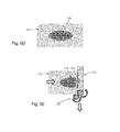
- the LED dies 102 are singulated from the wafer by pressing on the back of the wafer 110 with an anvil 123 .
- the wafer is located on a table 127 or other suitable surface having a gap 129 opposite the anvil 123 .
- FIG. 6 is a photograph of a singulated die made according to the above method. The plane 118 of defects 120 is clearly visible in the photograph.
- Stealth ScribingTM involves the application of internal defects to a wafer by laser focusing, and then anvil breaking the wafer along the lines of defects.
- Stealth ScribingTM uses preferred crystalline orientations for cleaving as there is still a minimum force needed for anvil breaking to break the wafer. “Preferred crystalline orientations” means there are certain orientations that will cleave preferential to other non-preferred orientations.
- the present inventors realized that etching of the continuous compressive stress layer which is uniformly compressively stressing the substrate, raises the local stress at etched grooves, which aids the dicing process after generating a defect pattern in the substrate using a laser.
- a III-nitride buffer layer such as a GaN buffer layer
- a sapphire substrate may be selectively etched to form street grooves which expose the substrate, creating local areas of increasing stress. Increasing the local stress decreases the force needed to break the substrate. Internal defects are then applied using the laser, as described above. Because of the increased local stress, the substrate can be broken with less force (e.g. roll breaking instead of anvil breaking), and can theoretically break in patterns inconsistent with the sapphire crystal preferred cleaving orientation.
- the method of dicing the substrate shown in FIGS. 5A-5E includes depositing a continuous first layer 105 , such as a GaN buffer layer, over the substrate 110 , such as a sapphire wafer.
- the first layer 105 imparts a compressive stress to the substrate.
- the method also includes etching grooves 109 in the first layer 105 to increase local stress at the grooves compared to stress at the remainder of the first layer located over the substrate, as shown in FIG. 5B .
- the step of etching grooves 109 comprises etching street grooves in inactive regions through the LEDs (i.e., LED layers) 103 and through the first layer 105 to expose the substrate and to define a pattern of individual LED dies on a first side of the substrate.
- the method also includes generating a pattern 122 of defects 120 in the substrate with a laser beam, as shown in FIGS. 5C and 5D .
- the location of the defects 120 in the pattern 122 of defects substantially corresponds to a location of at least some of the grooves 109 , and preferably all of the grooves, in the in the first layer 105 .
- the street grooves 109 and the pattern 122 of defects 120 mimic a pattern of individual LED dies 102 .
- the method includes applying pressure to the substrate to dice the substrate along the grooves, as shown in FIG. 5E .
- the pressure may be applied by roll breaking using roller(s) 125 rolled on the substrate 110 to form LED dies 102 .
- street grooves 109 are etched through the LED layers 103 and the buffer layer 105 down the surface 109 of the wafer 110 (the front 110 F or device side of the wafer 110 ).
- the compressive stress due to the continuous layer on the substrate results in peak stress concentrated in the streets 109 in the GaN buffer layer 105 .
- This concentrated stress in the streets 109 aids in singulating the LED dies 102 in a controlled manner and reduces loss caused by cracks that might otherwise meander away from the streets 109 and damage adjacent dies 102 .
- the wafer 110 is then thinned and mounted front side 110 F onto a tape 112 or another support, as shown in FIG. 5C , which keeps the singulated dies 102 from scattering once they are singulated.
- laser damaged regions (i.e., defects) 120 may be introduced into the wafer 110 with a laser as described above. Damaged regions 120 may be introduced with the laser either through the top (device) side 110 F or the bottom (back) side 110 B of the wafer 110 .
- the pattern 122 of defects 120 preferably comprises a region of defects located less than 10 microns below a surface of the substrate 110 .
- the patterns 122 of defects shown in FIG. 5D are for illustration purposes only. Other patterns may be produced as desired.
- the pattern 122 illustrated in FIG. 5D results in asymmetrically shaped LED dies 102 while the pattern 122 illustrated in FIG. 4C results in symmetrically shaped LED dies 102 .
- the wafer 110 is weakened in the locations that define the shape of the LED dies 102 .
- the wafer 110 is then subjected to roll breaking with rollers 125 , as shown in FIG. 5E .
- rollers 125 In an embodiment, two counter rotating rollers are used to singulate the LED dies 102 .
- the substrate 110 may cleaved along a non-preferred crystalline cleaving orientation during the step of applying pressure to the substrate to dice the substrate along the grooves 109 .
- LED dies 102 with symmetric and asymmetric die shapes can be made as shown in FIGS. 4D and 5E .
- FIGS. 7-11 illustrate submounts 124 according to other embodiments.
- the submount 124 is fabricated with standard metal interconnects, described in more detail below, prior to attaching the dies 102 .
- the submount 124 includes symmetrical tubs 126 in which the LED dies 102 are located.
- the submount 124 includes asymmetrical tubs 126 A with the same asymmetric shape as the asymmetrical LED dies 102 A.
- Several different asymmetric tub 126 A shapes can be etched into the submount 124 which allows for several different LED dies 102 A to be integrated into the submount 124 , as illustrated in FIG. 8 .
- the submount 124 is made of silicon.
- Another embodiment is drawn to a method of integrating asymmetrical LED dies 102 A into a submount 124 having asymmetrical tubs 126 A as illustrated in FIG. 7 .
- the individual asymmetrical LED dies 102 A are dispensed onto the submount 124 while the submount is vibrated. This agitation aids in the placement of the correct asymmetrical LED dies 102 A fitting into the corresponding asymmetrical tub 126 A.
- Preferably, only one combination of die and tub is possible.
- the x-y asymmetry assures the correct side of the asymmetrical LED die 126 A is “face up” (else the asymmetrical LED die 126 A does not fall into the asymmetrical tub 126 A).
- Eutectic bonding is a metallurgical reaction between two different metals with heating in which the metal form an alloy at a temperature below the melting temperature of either of the metals.
- a film of one metal is deposited on the bottoms of the asymmetrical LED dies 126 A and a film of the other metal is deposited in the asymmetrical tubs 126 A.
- An example of a suitable eutectic reaction for die attachment is Au—Sn. Gold and tin form an alloy upon heating to approximately 280° C.
- the metal interconnects are fabricated in the submount 124 before integrating the asymmetrical LED dies 102 A.
- the asymmetrical LED dies 102 A can be wire bonded to the pad on the metal interconnects, as described in more details below.
- Wire interconnects on the submount 124 may be fabricated by standard silicon processing techniques prior to assembly of the LED device 100 .
- the front side of the dies 124 may be electrically connected to the metal interconnects in the submount 124 by a direct write process, such as ink jet deposition of metal interconnects.
- an encapsulant may be deposited over the LED dies 102 A.
- the interconnects may be deposited from the asymmetrical LEDs 102 A to the submount 124 by direct write via inkjet printing of metal and deposition and patterning of a photoactive polyimide material. That is, in this embodiment, all of the metal interconnects are fabricated after the LED dies 102 A are assembled into the submount 124 . Multiple layers of metal interconnects may be made by a direct write process using ink jet deposition of metal connects and deposition and patterning of a photoactive polyimide that acts as an insulator between the layers of metal interconnects.
- encapsulant can be deposited over the asymmetrical LED dies 102 A with standard encapsulant techniques.
- FIGS. 8-11 illustrate a silicon submount 124 suitable for use with an integrated back light unit according to another embodiment.
- the submount 124 include integrated multilevel interconnect fabrication with the submount, selective Ni/Ag plating of the tubs onto highly doped Si, and deep Si etch of tubs over existing multilevel interconnect stacks.
- FIG. 8 is a plan view of the submount 124 while FIGS. 9 and 10 are cross-sectional views of the submount 124 through lines AA and BB, respectively.
- the cross section illustrated in FIG. 9 is through one of the tubs 126 prior to attachment of an LED die 102 .
- the cross section illustrated in FIG. 10 is through a pad area between tubs 102 .
- FIG. 11 is a three dimensional cut away view illustrating a portion of the submount of FIG. 8 .
- Each symmetric tub 126 is configured to hold an LED die 102 .
- the tubs 126 are preferably tapered. That is, the bottom of the tub 124 in which each LED die 102 is located has a width w b equal to or slightly larger than the width of the LED die 102 while the top of the tub 126 has a width w t larger than w b .
- the top width w t is larger than w b to aid in locating the LED dies 102 into the tubs 126 .
- the submount 124 includes three symmetric tubs 126 .
- a first tub 126 includes a red LED die 102 R
- a second tub 126 includes a green LED die 102 G
- the third tub includes a blue LED die 102 B.
- all of the tubs 126 may include LED dies that emit the same color of light.
- the submount 124 is not limited to three tubs 126 .
- the submount 124 may have any number of tubs 126 , such as 2-72, such as 3-60 tubs, such as 6-48 tubs.
- a segment is defined as three tubs 126 , typically including one red LED die 102 R, one green LED die 102 G and one blue LED die 102 B.
- the submount may include 1-24 segments, such as 2-20 segments, such as 3-16 segments.
- the submount 124 includes metal pads 128 between the tubs 126 for wire bonding. By placing the metal pads 128 between the tubs 126 rather than along the sides as in conventional submounts, the width of the submount can be reduced.
- Each LED die 102 includes corresponding bond pads 130 .
- Wire bonds 136 connect the metal pads 128 on the submount 124 to the corresponding bond pads 130 on the LED dies 102 .
- metal lines M1-M4 which are used to supply current to the LED dies 102 . While four lines are shown, other number of lines may be used. As illustrated in FIGS. 10 and 11 , the metal lines M may be located in different levels within the submount 124 such that there are four levels M1, M2, M3, M4.
- the submount 124 also includes metal landing pads 134 with vias on top to bring power to the metal lines M1, M2, M3, M4.
- lines M4 may be bus lines which provide current to electrode lines M1, M2, M3 which connect to the LED die. As illustrated, the metal landing pads 134 are square. However, the metal landing pads 134 may be circular, rectangular, hexagonal or any other suitable shape. Also illustrated in FIG.
- the metal film 138 material e.g., Au—Sn or Ni—Al
- the metal film 138 material is selected to react with a second metal film (not shown) on the bottom of the LED dies 102 to form a eutectic bond as discussed above.
- the submount is made of silicon and includes integrated interconnects for an integrated back light unit. In an embodiment:
- the submount 124 may be 530 ⁇ m wide and 33,120 ⁇ m long, not including pads to contact to the outside for power. Add 300 ⁇ m to the length for the 6 pads that will attach to the outside world and the submount 124 length is 33,420 ⁇ m. On a 200 mm Si wafer with 3 mm edge exclusion, this enables 1355 submounts 124 per wafer.
- An embodiment is drawn to a method of making the above submount 124 .
- One aspect of the embodiment of the method includes the following process flow:
- Both Al and SiO 2 have excellent resistance erosion during silicon etch. When these materials are combined with a thick photoresist and time multiplexed deep silicon etch techniques, there is sufficient margin to etch 300 ⁇ m of silicon without significant erosion of features that are masked from the etch. Electroless nickel plating of silicon is an established technique to metallize silicon. Subsequent silver plating the nickel is also an established technique, and allows for the selective plating of the tubs while not plating the SiO 2 -covered areas. Silicon submounts have advantages in wafer level packaging (high productivity fabrication), superior heat sink capability of silicon compared to more standard composite packages, and better thermal expansion match between silicon and sapphire compared to sapphire and composite packages.
Landscapes
- Engineering & Computer Science (AREA)
- Physics & Mathematics (AREA)
- Optics & Photonics (AREA)
- Plasma & Fusion (AREA)
- Mechanical Engineering (AREA)
- Chemical & Material Sciences (AREA)
- Chemical Kinetics & Catalysis (AREA)
- General Chemical & Material Sciences (AREA)
- Oil, Petroleum & Natural Gas (AREA)
- Led Devices (AREA)
- Microelectronics & Electronic Packaging (AREA)
Abstract
Description
-
- 1. Red, green, and blue LED dies 102R, 102G, 102B are 6-12, such as 8-10 mils square, e.g., a maximum of 210 μm. However, in alternative embodiments, other size LED dies 102 may be used;
- 2. A 365 nm contact lithography stepper may be used to produce line/spaces of 5 μm/5 μm;
- 3. The
tubs 126 may be 200-400 μm deep, such as 300 μm deep with 65-85 degree sloped sidewalls, such as 80 degree sidewalls; - 4. The
tubs 126 preferably have reflectors (i.e., film 138) on the bottom and sidewalls; - 5. The street widths are less than 150 μm, such as 100 μm, if conventionally scribed and may be less if stealth scribed;
- 6. Al may be used as a hard mask when deep etching a Si submount. In alternative embodiments, a more refractory metal than Si, such as Cr, Ti, TiN, TiW, or W may be used on top of Al to resist the Si etch.
-
- 1. Starting material: mechanical grade highly doped 200 mm Si wafers;
- 2. Deposit or grow 1000 Å SiO2 film on the Si wafer; thickness can be anywhere from 200 Å to 10 μm. Alternately, photoactive polyimide can be used in place of the SiO2, or other dielectrics, such as low-k SiCOH, SiN, Al2O3, etc dielectrics.
- 3. Pattern 300 Å Ti/1 μm Al (thin Ti for adhesion) lines on the SiO2 by a lift off technique or mask and etch (
metal 1, or M1); thicknesses can be anywhere from 50 Å to 1 μm of Ti and 2000 Å to 3 μm Al. Alternately there can be an antireflective coating on top of Al, typically Ti, TiN, WN, or Cr; - 4. Deposit a second SiO2 film 1 micron thick on top of M1; thickness can be anywhere from 200 Å to 10 μm, although in general, it should scale with the thickness of the metal;
- 5. Deposit a second Ti/Al line, or M2, on top of the second SiO2 film;
- 6. Deposit a third SiO2 film on top of M2;
- 7. Deposit a third Ti/Al film M3 on top of the third SiO2 film;
- 8. Deposit a fourth SiO2 film on top of M3;
- 9. Pattern the fourth oxide film and dry etch SiO2 to open the vias and pads to M1, M2, & M3;
- 10. Deposit, pattern, and etch Ti/Al film M4 on top of the fourth SiO2 film; with the pads to M1, M2, and M3 open, M4 will now connect to the lower metal layers. M4 is called the bus line(s). In an embodiment, there are 6 discrete interconnects in M4, allowing n and p connections to the red, green, and blue LED. The LED can be connected in series or parallel at the designer's discretion. If a via connects each die to the bus line, then all LED are connected in parallel. If there are only vias at the first and last (e.g., 72nd) LED, then the LED are connected in series. Any other combination is also possible (e.g. connect every 3rd red LED, so that there are 3 in series, and that group of 3 is connected in parallel to 8 other groups of 3);
- 11. Deposit a fifth SiO2 film on top of M4; This final SiO2 film forms the passivation;
- 12. Pattern the tubs, and proceed to dry etch the SiO2;
- 13. Dry etch 300 μm deep tubs into the Si wafer. The tubs can be skipped (0 um deep, or can be anywhere from 100 to 500 μm deep);
- 14. After Si etch, electroplate Ni/Ag into the exposed conductive Si. Typical Ni/Ag thicknesses are 300 Å Ni/2000 Å Ag. Nickel thickness can range from 50 Å to 5000 Å, and silver thickness can range from 500 Å to 5 μm;
- 15. Singulate LED die using sawing or any of the other singulation methods described herein;
- 16. Die attach by eutectic bonding or by epoxy or silicone adhesive, followed by curing of same;
- 17. Wire bond, e.g. with Au wire bonds;
- 18. Encapsulate, e.g. using silicone, which can alternately have a phosphor powder embedded in it, converting the LED's light from one wavelength to another.
Claims (9)
Priority Applications (1)
| Application Number | Priority Date | Filing Date | Title |
|---|---|---|---|
| US14/550,121 US9412899B2 (en) | 2013-11-22 | 2014-11-21 | Method of stress induced cleaving of semiconductor devices |
Applications Claiming Priority (2)
| Application Number | Priority Date | Filing Date | Title |
|---|---|---|---|
| US201361907487P | 2013-11-22 | 2013-11-22 | |
| US14/550,121 US9412899B2 (en) | 2013-11-22 | 2014-11-21 | Method of stress induced cleaving of semiconductor devices |
Publications (2)
| Publication Number | Publication Date |
|---|---|
| US20150144968A1 US20150144968A1 (en) | 2015-05-28 |
| US9412899B2 true US9412899B2 (en) | 2016-08-09 |
Family
ID=53180207
Family Applications (1)
| Application Number | Title | Priority Date | Filing Date |
|---|---|---|---|
| US14/550,121 Active US9412899B2 (en) | 2013-11-22 | 2014-11-21 | Method of stress induced cleaving of semiconductor devices |
Country Status (3)
| Country | Link |
|---|---|
| US (1) | US9412899B2 (en) |
| TW (1) | TW201532303A (en) |
| WO (1) | WO2015077612A1 (en) |
Cited By (2)
| Publication number | Priority date | Publication date | Assignee | Title |
|---|---|---|---|---|
| US11637219B2 (en) | 2019-04-12 | 2023-04-25 | Google Llc | Monolithic integration of different light emitting structures on a same substrate |
| US11784160B2 (en) | 2020-09-23 | 2023-10-10 | International Business Machines Corporation | Asymmetric die bonding |
Families Citing this family (3)
| Publication number | Priority date | Publication date | Assignee | Title |
|---|---|---|---|---|
| CN111183514B (en) * | 2017-10-30 | 2022-12-27 | 华为技术有限公司 | Device and method for cutting display panel from mother substrate |
| US11137356B2 (en) * | 2017-11-03 | 2021-10-05 | Sela Semiconductor Engineering Laboratories Ltd. | System and method of cleaving of buried defects |
| CN111725360B (en) * | 2019-03-22 | 2023-04-07 | 安徽三安光电有限公司 | Composite substrate, preparation method thereof and method for preparing light-emitting element by using composite substrate |
Citations (5)
| Publication number | Priority date | Publication date | Assignee | Title |
|---|---|---|---|---|
| JP2006245062A (en) | 2005-02-28 | 2006-09-14 | Toyoda Gosei Co Ltd | Method of manufacturing group iii nitride-based compound semiconductor element, and light emitting element |
| WO2007046656A1 (en) | 2005-10-20 | 2007-04-26 | Bnp Science | Method of producing light emitting diode having vertical structure |
| US20110159615A1 (en) | 2009-12-28 | 2011-06-30 | Hon Hai Precision Industry Co., Ltd. | Led units fabrication method |
| US20120083059A1 (en) | 2010-09-30 | 2012-04-05 | Disco Corporation | Sapphire wafer dividing method |
| US20130095260A1 (en) | 2005-09-08 | 2013-04-18 | Imra America, Inc. | Transparent material processing with an ultrashort pulse laser |
-
2014
- 2014-11-21 WO PCT/US2014/066899 patent/WO2015077612A1/en not_active Ceased
- 2014-11-21 US US14/550,121 patent/US9412899B2/en active Active
- 2014-11-24 TW TW103140695A patent/TW201532303A/en unknown
Patent Citations (6)
| Publication number | Priority date | Publication date | Assignee | Title |
|---|---|---|---|---|
| JP2006245062A (en) | 2005-02-28 | 2006-09-14 | Toyoda Gosei Co Ltd | Method of manufacturing group iii nitride-based compound semiconductor element, and light emitting element |
| US20130095260A1 (en) | 2005-09-08 | 2013-04-18 | Imra America, Inc. | Transparent material processing with an ultrashort pulse laser |
| WO2007046656A1 (en) | 2005-10-20 | 2007-04-26 | Bnp Science | Method of producing light emitting diode having vertical structure |
| US20110159615A1 (en) | 2009-12-28 | 2011-06-30 | Hon Hai Precision Industry Co., Ltd. | Led units fabrication method |
| US20120083059A1 (en) | 2010-09-30 | 2012-04-05 | Disco Corporation | Sapphire wafer dividing method |
| KR20120033962A (en) | 2010-09-30 | 2012-04-09 | 가부시기가이샤 디스코 | Method for dividing sapphire wafer |
Non-Patent Citations (2)
| Title |
|---|
| International Preliminary Report on Patentability for International Application No. PCT/US2014/066899, 9 pages, dated Jun. 2, 2016. |
| International Search Report and Written Opinion recevied in connection with international application No. PCT/US2014/066899; mailed Mar. 27, 2015. |
Cited By (3)
| Publication number | Priority date | Publication date | Assignee | Title |
|---|---|---|---|---|
| US11637219B2 (en) | 2019-04-12 | 2023-04-25 | Google Llc | Monolithic integration of different light emitting structures on a same substrate |
| US12191418B2 (en) | 2019-04-12 | 2025-01-07 | Google Llc | Monolithic integration of different light emitting structures on a same substrate |
| US11784160B2 (en) | 2020-09-23 | 2023-10-10 | International Business Machines Corporation | Asymmetric die bonding |
Also Published As
| Publication number | Publication date |
|---|---|
| US20150144968A1 (en) | 2015-05-28 |
| WO2015077612A1 (en) | 2015-05-28 |
| TW201532303A (en) | 2015-08-16 |
Similar Documents
| Publication | Publication Date | Title |
|---|---|---|
| US9287468B2 (en) | LED submount with integrated interconnects | |
| US12132155B2 (en) | Etched trenches in bond materials for die singulation, and associated systems and methods | |
| US9478722B2 (en) | Light emitting device and method for manufacturing same | |
| CN106537616B (en) | light-emitting device | |
| JP3904585B2 (en) | Manufacturing method of semiconductor device | |
| JP3959988B2 (en) | Element transfer method | |
| US20060214173A1 (en) | Light emitting diodes and methods of fabrication | |
| JP2011253925A (en) | Method of manufacturing light-emitting device | |
| US9412899B2 (en) | Method of stress induced cleaving of semiconductor devices | |
| JP6555335B2 (en) | LIGHT EMITTING DEVICE AND LIGHT EMITTING DEVICE MANUFACTURING METHOD | |
| US20190189597A1 (en) | Discontinuous patterned bonds for semiconductor devices and associated systems and methods | |
| KR20110031999A (en) | Semiconductor light emitting device comprising a window layer and a light directing structure | |
| CN101183701A (en) | A kind of LED chip and preparation method thereof | |
| CN112768484A (en) | Light emitting diode and manufacturing method thereof | |
| US20150179894A1 (en) | Methods of locating differently shaped or differently sized led die in a submount | |
| TW201351730A (en) | Device module | |
| JP6269753B2 (en) | Light emitting device | |
| JP2001274458A (en) | Semiconductor light emitting device and method of manufacturing the same | |
| JP2006203251A (en) | Production method for semiconductor device | |
| KR100762093B1 (en) | Vertical light emitting device and package manufacturing method | |
| KR100820822B1 (en) | Vertical light emitting device and package manufacturing method | |
| KR20250018104A (en) | Semiconductor device arrangement structure and method of manufacturing the same | |
| CN121843311A (en) | Micro-light-emitting structures and their fabrication methods, as well as micro-light-emitting devices |
Legal Events
| Date | Code | Title | Description |
|---|---|---|---|
| AS | Assignment |
Owner name: GLO AB, SWEDEN Free format text: ASSIGNMENT OF ASSIGNORS INTEREST;ASSIGNORS:HERNER, SCOTT BRAD;ROMANO, LINDA;THOMPSON, DANIEL BRYCE;AND OTHERS;SIGNING DATES FROM 20150121 TO 20150129;REEL/FRAME:037882/0691 |
|
| STCF | Information on status: patent grant |
Free format text: PATENTED CASE |
|
| AS | Assignment |
Owner name: HERCULES CAPITAL, INC., AS ADMINISTRATIVE AGENT, M Free format text: ASSIGNMENT OF IP SECURITY AGREEMENT;ASSIGNOR:GLO AB;REEL/FRAME:049042/0527 Effective date: 20180108 Owner name: HERCULES CAPITAL, INC., AS ADMINISTRATIVE AGENT, MASSACHUSETTS Free format text: ASSIGNMENT OF IP SECURITY AGREEMENT;ASSIGNOR:GLO AB;REEL/FRAME:049042/0527 Effective date: 20180108 |
|
| AS | Assignment |
Owner name: HERCULES CAPITAL INC., CALIFORNIA Free format text: SECURITY INTEREST;ASSIGNOR:GLO AB;REEL/FRAME:048110/0063 Effective date: 20180108 |
|
| FEPP | Fee payment procedure |
Free format text: MAINTENANCE FEE REMINDER MAILED (ORIGINAL EVENT CODE: REM.); ENTITY STATUS OF PATENT OWNER: SMALL ENTITY |
|
| FEPP | Fee payment procedure |
Free format text: SURCHARGE FOR LATE PAYMENT, SMALL ENTITY (ORIGINAL EVENT CODE: M2554); ENTITY STATUS OF PATENT OWNER: SMALL ENTITY |
|
| MAFP | Maintenance fee payment |
Free format text: PAYMENT OF MAINTENANCE FEE, 4TH YR, SMALL ENTITY (ORIGINAL EVENT CODE: M2551); ENTITY STATUS OF PATENT OWNER: SMALL ENTITY Year of fee payment: 4 |
|
| AS | Assignment |
Owner name: GLO AB, SWEDEN Free format text: RELEASE BY SECURED PARTY;ASSIGNOR:HERCULES CAPITAL, INC.;REEL/FRAME:057210/0690 Effective date: 20210329 Owner name: GLO AB, SWEDEN Free format text: RELEASE OF SECURITY INTEREST;ASSIGNOR:HERCULES CAPITAL, INC.;REEL/FRAME:057210/0690 Effective date: 20210329 |
|
| AS | Assignment |
Owner name: NANOSYS, INC., CALIFORNIA Free format text: NUNC PRO TUNC ASSIGNMENT;ASSIGNOR:GLO AB;REEL/FRAME:057184/0564 Effective date: 20210809 |
|
| AS | Assignment |
Owner name: FORTRESS CREDIT CORP., AS AGENT, NEW YORK Free format text: SECURITY INTEREST;ASSIGNOR:NANOSYS, INC.;REEL/FRAME:059569/0840 Effective date: 20220401 |
|
| AS | Assignment |
Owner name: NANOSYS, INC., CALIFORNIA Free format text: TERMINATION AND RELEASE OF PATENT SECURITY AGREEMENT RECORDED AT REEL 059569 / FRAME 0840;ASSIGNOR:FORTRESS CREDIT CORP.,;REEL/FRAME:064836/0263 Effective date: 20230906 |
|
| AS | Assignment |
Owner name: SYSONAN, INC., CALIFORNIA Free format text: CHANGE OF NAME;ASSIGNOR:NANOSYS, INC.;REEL/FRAME:065156/0416 Effective date: 20230911 |
|
| AS | Assignment |
Owner name: GLO TECHNOLOGIES LLC, CALIFORNIA Free format text: ASSIGNMENT OF ASSIGNORS INTEREST;ASSIGNOR:SYSONAN, INC.;REEL/FRAME:065178/0210 Effective date: 20231004 |
|
| FEPP | Fee payment procedure |
Free format text: MAINTENANCE FEE REMINDER MAILED (ORIGINAL EVENT CODE: REM.); ENTITY STATUS OF PATENT OWNER: SMALL ENTITY |
|
| AS | Assignment |
Owner name: SAMSUNG ELECTRONICS CO., LTD., KOREA, REPUBLIC OF Free format text: ASSIGNMENT OF ASSIGNORS INTEREST;ASSIGNOR:GLO TECHNOLOGIES LLC;REEL/FRAME:068297/0220 Effective date: 20240611 |
|
| FEPP | Fee payment procedure |
Free format text: 7.5 YR SURCHARGE - LATE PMT W/IN 6 MO, SMALL ENTITY (ORIGINAL EVENT CODE: M2555); ENTITY STATUS OF PATENT OWNER: SMALL ENTITY |
|
| MAFP | Maintenance fee payment |
Free format text: PAYMENT OF MAINTENANCE FEE, 8TH YR, SMALL ENTITY (ORIGINAL EVENT CODE: M2552); ENTITY STATUS OF PATENT OWNER: SMALL ENTITY Year of fee payment: 8 |