US9412784B1 - Pre-flash time adjusting circuit and image sensor using the same - Google Patents

Pre-flash time adjusting circuit and image sensor using the same Download PDF

Info

Publication number
US9412784B1
US9412784B1 US14/873,607 US201514873607A US9412784B1 US 9412784 B1 US9412784 B1 US 9412784B1 US 201514873607 A US201514873607 A US 201514873607A US 9412784 B1 US9412784 B1 US 9412784B1
Authority
US
United States
Prior art keywords
storage capacitor
flash time
pixel units
time adjusting
sensing array
Prior art date
Legal status (The legal status is an assumption and is not a legal conclusion. Google has not performed a legal analysis and makes no representation as to the accuracy of the status listed.)
Active
Application number
US14/873,607
Inventor
Wooi-Kip Lim
Current Assignee (The listed assignees may be inaccurate. Google has not performed a legal analysis and makes no representation or warranty as to the accuracy of the list.)
Pixart Imaging Penang Sdn Bhd
Original Assignee
Pixart Imaging Penang Sdn Bhd
Priority date (The priority date is an assumption and is not a legal conclusion. Google has not performed a legal analysis and makes no representation as to the accuracy of the date listed.)
Filing date
Publication date
Application filed by Pixart Imaging Penang Sdn Bhd filed Critical Pixart Imaging Penang Sdn Bhd
Priority to US14/873,607 priority Critical patent/US9412784B1/en
Assigned to PIXART IMAGING (PENANG) SDN. BHD. reassignment PIXART IMAGING (PENANG) SDN. BHD. ASSIGNMENT OF ASSIGNORS INTEREST (SEE DOCUMENT FOR DETAILS). Assignors: LIM, WOOI-KIP
Priority to TW104144448A priority patent/TWI544746B/en
Priority to CN201610028513.2A priority patent/CN106561048B/en
Application granted granted Critical
Publication of US9412784B1 publication Critical patent/US9412784B1/en
Active legal-status Critical Current
Anticipated expiration legal-status Critical

Links

Images

Classifications

    • H01L27/14681
    • HELECTRICITY
    • H10SEMICONDUCTOR DEVICES; ELECTRIC SOLID-STATE DEVICES NOT OTHERWISE PROVIDED FOR
    • H10FINORGANIC SEMICONDUCTOR DEVICES SENSITIVE TO INFRARED RADIATION, LIGHT, ELECTROMAGNETIC RADIATION OF SHORTER WAVELENGTH OR CORPUSCULAR RADIATION
    • H10F39/00Integrated devices, or assemblies of multiple devices, comprising at least one element covered by group H10F30/00, e.g. radiation detectors comprising photodiode arrays
    • H10F39/10Integrated devices
    • H10F39/12Image sensors
    • H10F39/197Bipolar transistor image sensors
    • GPHYSICS
    • G06COMPUTING OR CALCULATING; COUNTING
    • G06FELECTRIC DIGITAL DATA PROCESSING
    • G06F3/00Input arrangements for transferring data to be processed into a form capable of being handled by the computer; Output arrangements for transferring data from processing unit to output unit, e.g. interface arrangements
    • G06F3/01Input arrangements or combined input and output arrangements for interaction between user and computer
    • G06F3/03Arrangements for converting the position or the displacement of a member into a coded form
    • G06F3/0304Detection arrangements using opto-electronic means
    • G06F3/0317Detection arrangements using opto-electronic means in co-operation with a patterned surface, e.g. absolute position or relative movement detection for an optical mouse or pen positioned with respect to a coded surface
    • HELECTRICITY
    • H04ELECTRIC COMMUNICATION TECHNIQUE
    • H04NPICTORIAL COMMUNICATION, e.g. TELEVISION
    • H04N25/00Circuitry of solid-state image sensors [SSIS]; Control thereof
    • H04N25/70SSIS architectures; Circuits associated therewith
    • GPHYSICS
    • G06COMPUTING OR CALCULATING; COUNTING
    • G06FELECTRIC DIGITAL DATA PROCESSING
    • G06F3/00Input arrangements for transferring data to be processed into a form capable of being handled by the computer; Output arrangements for transferring data from processing unit to output unit, e.g. interface arrangements
    • G06F3/01Input arrangements or combined input and output arrangements for interaction between user and computer
    • G06F3/03Arrangements for converting the position or the displacement of a member into a coded form
    • G06F3/033Pointing devices displaced or positioned by the user, e.g. mice, trackballs, pens or joysticks; Accessories therefor
    • G06F3/038Control and interface arrangements therefor, e.g. drivers or device-embedded control circuitry
    • HELECTRICITY
    • H04ELECTRIC COMMUNICATION TECHNIQUE
    • H04NPICTORIAL COMMUNICATION, e.g. TELEVISION
    • H04N25/00Circuitry of solid-state image sensors [SSIS]; Control thereof
    • H04N25/50Control of the SSIS exposure
    • GPHYSICS
    • G06COMPUTING OR CALCULATING; COUNTING
    • G06FELECTRIC DIGITAL DATA PROCESSING
    • G06F3/00Input arrangements for transferring data to be processed into a form capable of being handled by the computer; Output arrangements for transferring data from processing unit to output unit, e.g. interface arrangements
    • G06F3/01Input arrangements or combined input and output arrangements for interaction between user and computer
    • G06F3/03Arrangements for converting the position or the displacement of a member into a coded form
    • G06F3/033Pointing devices displaced or positioned by the user, e.g. mice, trackballs, pens or joysticks; Accessories therefor
    • G06F3/0354Pointing devices displaced or positioned by the user, e.g. mice, trackballs, pens or joysticks; Accessories therefor with detection of 2D relative movements between the device, or an operating part thereof, and a plane or surface, e.g. 2D mice, trackballs, pens or pucks
    • G06F3/03543Mice or pucks

Definitions

  • the present disclosure relates to a pre-flash time adjusting circuit, in particular, to a pre-flash time adjusting circuit which can adaptively adjust a pre-flash time of the image sensing array and image sensor thereof.
  • An optical mouse typically includes a light source (such as a light-emitting diode) to illuminate a working surface and an image sensor that functions as a miniature digital camera to continually capture images of the illuminated working surface and to determine the speed and direction that the optical mouse is being moved across the surface by comparing sequentially captured frames of image information so as to control the movement of a cursor displayed on a monitor.
  • a light source such as a light-emitting diode
  • an image sensor that functions as a miniature digital camera to continually capture images of the illuminated working surface and to determine the speed and direction that the optical mouse is being moved across the surface by comparing sequentially captured frames of image information so as to control the movement of a cursor displayed on a monitor.
  • the image sensor includes an image sensing array.
  • the image sensing array includes a plurality of pixel units for capturing image of the illuminated working surface. Please refer to FIG. 1 and FIG. 2 .
  • FIG. 1 is schematic diagram illustrating a conventional pixel unit.
  • FIG. 2 is a timing waveform diagram illustrating the operation of the conventional pixel unit.
  • the pixel unit 15 includes a PMOS transistor MP 1 , a NMOS transistor MN 1 , a NMOS transistor MN 2 , a NMOS transistor MN 3 , a PMOS transistor MP 2 , a bipolar junction transistor (hereinafter BJT transistor) Q, a photodetector PD and a capacitor C.
  • the PMOS transistor MP 1 , the NMOS transistor MN 1 and the NMOS transistor MN 2 compose a feedback amplifier circuit 150 .
  • the NMOS transistor MN 3 and the PMOS transistor MP 2 compose a shutter circuit 151 .
  • the feedback amplifier circuit 150 , the shutter circuit 151 and the photodetector PD are respectively coupled to the BJT transistor Q.
  • the capacitor C is coupled to the shutter circuit 151 and the ground.
  • the capacitor C is configured for operatively storing the image data captured by the photodetector PD.
  • a light-emitting diode (not shown in FIG. 1 ) provides a light beam to illuminate the working surface, and the working surface reflects the light beam and generates a reflected light beam.
  • the photodetector PD operatively generates a base current IB in responsive to a light intensity of the reflected light.
  • the feedback amplifier circuit 150 begins to build up a base-emitter voltage V BE of the BJT transistor Q to increase the beta of the BJT transistor Q to a stable state e.g., ⁇ 30.
  • the beta herein is the ratio between the collector current IC and the base current IB of the BJT transistor Q.
  • the BJT transistor Q When the BJT transistor Q reaches the stable state, the BJT transistor Q operates with a stable beta and generates a stable emitter current IE.
  • the shutter circuit 151 is triggered on by a shutter signal such that the storage capacitor C can be discharged with a stable emitter current IE to capture the image data. Accordingly, when the shutter circuit 151 is triggered on, the voltage across the capacitor C decreases as the capacitor C discharges through BJT transistor Q with the emitter current IE.
  • the time required from the light-emitting diode turning on (the base-emitter voltage V BE of the BJT transistor Q starts to increase) to the time the BJT transistor Q reaching the stable state is defined as the pre-flash time of the BJT pixel circuit Q.
  • the time required from the shutter circuit being triggered on until the completion of image capturing is defined as an exposure time.
  • the pre-flash time is set to about 220 microseconds (us), and the exposure time is set to about 10 us.
  • the pre-flash time required by the pixel unit 15 will be different.
  • the darker image data needs enough pre-flash time.
  • the brighter image does not need too long pre-flash time. Because the conventional image sensor fixes the pre-flash time, when the pixel unit 15 captures the brighter image data, the pre-flash time does not end as soon as the base-emitter voltage V BE of the BJT transistor Q reaches the stable state. The light-emitting unit will waste power if the image sensor operates with the fixed pre-flash time.
  • An exemplary embodiment of the present disclosure provides a pre-flash time adjusting circuit which comprises a first pre-flash time adjusting unit coupled to an image sensing array.
  • the image sensing array comprises a plurality of pixel units.
  • the first pre-flash time adjusting unit comprises a switching module and a storage capacitor.
  • a first switch of the switching module is coupled to a first pixel group of the image sensing array, and a second switch of the switching module is coupled to a voltage source.
  • a first end of the storage capacitor is coupled to the switching module, and a second end of the storage capacitor is coupled to ground.
  • the first pixel group comprises a plurality of first pixel units of the pixel units.
  • the switching module selectively connects the first switch and the storage capacitor, such that the storage capacitor starts to charge the first pixel units of the first pixel group, until base-emitter voltages of a plurality of bipolar junction transistors disposed in the first pixel units reaches a stable state.
  • An exemplary embodiment of the present disclosure provides an image sensor.
  • the image sensor comprises an image sensing array and a pre-flash time adjusting circuit.
  • the image sensing array comprises a plurality of pixel units.
  • the pre-flash time adjusting circuit comprises a first pre-flash time adjusting unit coupled to the image sensing array.
  • the first pre-flash time adjusting unit comprises a switching module and a storage capacitor.
  • a first switch of the switching module is coupled to a first pixel group of the image sensing array, and a second switch of the switching module is coupled to a voltage source.
  • a first end of the storage capacitor is coupled to a third end of the switching module, and a second end of the storage capacitor is coupled to ground.
  • the first pixel group comprises a plurality of first pixel units of the pixel units.
  • the switching module selectively connects the first switch and the storage capacitor, such that the storage capacitor starts to charge the first pixel units of the first pixel group, until base-emitter voltages of a plurality of bipolar junction transistors disposed in the first pixel units reach a stable state.
  • the pre-flash time adjusting circuit and the image sensor provided by the present disclosure can adaptively adjust the pre-flash time of the pixel units of the image sensing array in response to the brightness of the image data associated with the working surface, and adjust working duration of the light-emitting unit disposed in the image sensor.
  • the pre-flash time adjusting circuit and the image sensor provided by the present disclosure reduces power consumption of the light-emitting unit effectively.
  • FIG. 1 is schematic diagram illustrating a conventional pixel unit.
  • FIG. 2 is a timing waveform diagram illustrating the operation of the conventional pixel unit.
  • FIG. 3 is a schematic diagram illustrating an image sensor provided in accordance to an exemplary embodiment of the present disclosure.
  • FIG. 6 is a schematic diagram illustrating an image sensor provided in accordance to another exemplary embodiment of the present disclosure.
  • first, second, third, etc. may be used herein to describe various elements or signals, but these signals should not be affected by such elements or terms. Such terminology is used to distinguish one element from another or a signal with another signal. Further, the term “or” as used herein in the case may include any one or combinations of the associated listed items.
  • the image sensing array 30 is a complementary metal-oxide semiconductor (CMOS) image sensing array, or a charge-coupled device (CCD) image sensing array.
  • CMOS complementary metal-oxide semiconductor
  • CCD charge-coupled device
  • the pre-flash time adjusting circuit 31 includes at least one pre-flash time adjusting unit 310 .
  • the pre-flash time adjusting unit 310 includes a switching module SW and a storage capacitor C S .
  • a first switch SW_ 1 of the switching module SW is coupled to the image sensing array 30 .
  • a second switch SW_ 2 of the switching module SW is coupled to a voltage source to receive a supply voltage VDD.
  • the switching module SW is coupled to a first end of the storage capacitor C S .
  • a second end of the storage capacitor C S is coupled to a ground.
  • the switching module SW is configured for selectively connecting the first switch SW_ 1 and the storage capacitor C S , or selectively connecting the second switch SW_ 2 and the storage capacitor C S .
  • the pre-flash time adjusting circuit 31 adaptively adjusts a pre-flash time of the image sensing array 30 , such that the image sensing array 30 captures the corresponding image data. By disposing the pre-flash time adjusting circuit 31 in the image sensing array 30 , the light-emitting unit LED can reduce power consumption.
  • a source of the PMOS transistor MP 1 _ 1 is coupled to the voltage source to receive the supply voltage VDD.
  • a gate of the PMOS transistor MP 1 _ 1 is coupled to a bias end to receive a bias voltage VBIAS.
  • a drain of the PMOS transistor MP 1 _ 1 is coupled to a drain of the NMOS transistor MN 2 _ 1 .
  • a gate of the NMOS transistor MN 2 _ 1 is coupled to a base of the BJT transistor Q 1 .
  • a source of the NMOS transistor MN 2 _ 1 is coupled to the ground.
  • a gate of the NMOS transistor MN 1 _ 1 is coupled to a drain of the PMOS transistor MP 1 _ 1 .
  • a drain of the NMOS transistor MN 3 _ 1 is coupled to a control end to receive a control voltage VRST 1 . Moreover, the drain of the NMOS transistor MN 3 _ 1 is further coupled to the first switch SW_ 1 of the switching module SW. A gate of the NMOS transistor MN 3 _ 1 is coupled to a gate of the PMOS transistor MP 2 _ 1 . The drain of the PMOS transistor MP 2 _ 1 is coupled to a source of the NMOS transistor MN 3 _ 1 . A gate of the PMOS transistor MP 2 _ 1 is coupled to a shutter end to receive a shutter signal SHUTTER. A source of the PMOS transistor MP 2 _ 1 is coupled to a first end of the first capacitor C 1 .
  • a collector of the BJT transistor Q 1 and a second end of the first capacitor C 1 are coupled to the ground. Additionally, a control circuit (not shown in FIG. 4 ) is respectively coupled to the bias end, the control end, and the shutter end to control the operation of the image sensing array 30 .
  • a cathode of the photodetector PD 1 is coupled to a base of the BJT transistor Q 1 .
  • An anode of the photodetector PD 1 is coupled to the ground.
  • the cathode of the photodetector PD 1 is further coupled to the base of the BJT transistor Q 1 .
  • the photodetector PD 1 is coupled between the base of the BJT transistor Q 1 and the ground.
  • the photodetector PD 1 may be implemented by a photodiode, however in practice, the photodetector PD 1 may be any light sensing element or circuit that transforms light intensity into a voltage value and the present disclosure is not limited thereto.
  • Structures of other pixel units included in the pixel group 300 are similar to the first pixel unit, thus their description is omitted. Incidentally, the structures of the pixel units described above are not limited to the examples provided by the instant embodiment.
  • the pixel units may be any circuits that can capture the image data and the present disclosure is not limited thereto.
  • the pre-flash time adjusting circuit 31 comprises a pre-flash time adjusting unit 310 and a comparator 311 .
  • the structure and the connection of the pre-flash time adjusting unit 310 are as described previously.
  • a non-inverting input end of the comparator 311 is coupled to the first end of the storage capacitor C S , and an inverting input end of the comparator 311 receives a threshold voltage V TH .
  • FIG. 5 shows a timing waveform diagram illustrating the operation of the image sensor.
  • the control circuit turns on the light-emitting unit LED to illuminate the working surface of the optical navigation device.
  • the photodetector PD 1 operatively generates a base current IB 1 based on the light intensity of a reflected light beam incident on the photodetector PD 1 , wherein the reflected light beam is the light reflected from the working surface illuminated by the light-emitting unit LED.
  • the control circuit outputs a first switching signal S 1 with a logic high level to the switching module SW, such that the switching module SW connects the first switch SW_ 1 and the storage capacitor C S .
  • the second switch SW_ 2 and storage capacitor C S are electrically isolated.
  • the storage capacitor C S starts providing the charge current IE TOL to charge the pixel units.
  • the PMOS transistor MP 1 _ 1 , the NMOS transistor MN 1 _ 1 and the NMOS transistor MN 2 _ 1 of the first pixel unit continues to operatively increase the base-emitter voltage V BE of the BJT transistor Q 1 so as to increase the beta of the BJT transistor Q 1 to a stable state (e.g., ⁇ 30) after the first pixel unit receives the charge current IE TOL through the NMOS transistor MN 3 _ 1 .
  • the beta herein is the ratio between the collector current IC 1 and the base current IB 1 of the BJT transistor Q 1 .
  • the BJT transistor Q 1 When the BJT transistor Q 1 reaches the stable state, the BJT transistor Q 1 operates with a stable base-emitter voltage V BE and generates a stable emitter current IE 1 .
  • the pre-flash time is defined as a period from when the base-emitter voltages V BE of the BJT transistors disposed in the pixel units begin to rise until the stable state.
  • Electric charge quantity stored in the storage capacitor C S decreases along with time because the storage capacitor C S continues to operatively provide the charge current IE TOL to the pixel units, which means that a voltage level V C of the first end of the storage capacitor C S will decrease along with time.
  • the voltage level V C of the first end of the storage capacitor C S is associated with the base-emitter voltages V BE of the pixel units.
  • the comparator 311 Before the voltage level V C of the first end of the storage capacitor C S is less than a threshold voltage V TH , the comparator 311 outputs a comparative signal V o with a logic high level to the control circuit.
  • the comparator 311 outputs the comparative signal V o with a logic low level to the control circuit.
  • the control circuit After sensing the logic level of the comparative signal V o changes from high to low, the control circuit outputs the first switching signal S 1 with a logic low level to the switching module SW.
  • the switching module SW electrically isolates the first switch SW_ 1 and the storage capacitor C S to finish the pre-flash time of the pixel units.
  • the control circuit outputs a second switching signal S 2 with a logic high level to the switching module SW.
  • the switching module SW connects the second switch SW_ 2 and the storage capacitor C S , and then the voltage level V C of the first end of the storage capacitor C S is reset to an initial voltage.
  • the control circuit outputs shutter signals SHUTTER with logic low level to the shutter ends of each pixel unit to begin the exposure time of the photodetectors PD 1 . . . PD n .
  • the PMOS transistors MP 2 _ 1 . . . MP 2 _ n are turning on and the NMOS transistors MN 3 _ 1 . . . MN 3 _ n are turning off During the exposure time, the first capacitor C 1 to the n-th capacitor C n of the pixel units stably discharge through the BJT transistor Q 1 . . . Q n with the emitter current IE 1 . . . IE n . Then, the pixel units capture the image data associated with the working surface.
  • the control circuit receives the comparative signal V o outputted by the comparator 311 , and then outputs the first switching signal S 1 , the second switching signal S 2 and the shutter signal SHUTTER in response to the comparative signal V o .
  • the present disclosure does not limit the duration of the gap time. In the current exemplary embodiment, the gap time is close to zero.
  • the pre-flash time adjusting circuit 31 provided by the present disclosure can adaptively adjust the pre-flash time of the pixel units based upon the brightness of the image data.
  • the light-emitting unit LED stops providing the light beam after the base-emitter voltages V BE of the BJT transistors Q 1 . . . Q n reach the stable state to save power.
  • the BJT transistors Q 1 . . . Q n may need only 30 us to reach the stable state. Then, the light-emitting unit LED turns on for 30 us to provide the light beam.
  • the image sensor 3 provided by the present disclosure can save 86% of the power consumed by the light-emitting unit LED.
  • duration of the exposure time is associated with duration of the pre-flash time, which means that the duration of the exposure time will vary in response to the brightness of the image data.
  • the control circuit stops providing current to the N-th pixel unit to save power.
  • FIG. 6 shows a schematic diagram illustrating an image sensor provided in accordance to another exemplary embodiment of the present disclosure.
  • a structure of the image sensor 6 shown in FIG. 6 is similar to the image sensor 3 shown in FIG. 3 , and therefore only differences between them will be described below.
  • the image sensor 6 also comprises an image sensing array 60 and a pre-flash time adjusting circuit 61 . Differences between the image sensor 3 and the image sensor 6 are that, a switching module SW′ of a pre-flash time adjusting unit 610 of the pre-flash time adjusting circuit 61 further comprises a third switch SW_ 3 ′ besides a first switch SW_ 1 ′ and a second switch SW_ 2 ′. Furthermore, the image sensing array 60 is divided into a first pixel group 600 and a second pixel group 601 . The first pixel group 600 and the second pixel group 601 respectively include a plurality of pixel units.
  • the first switch SW_ 1 ′ of the switching module SW′ is coupled to the first pixel group 600 .
  • the second switch SW_ 2 ′ of the switching module SW′ is coupled to a voltage source to receive a supply voltage VDD.
  • the switching module SW′ is coupled to a first end of the storage capacitor C S ′.
  • a second end of the storage capacitor C S ′ is coupled to a ground.
  • the third switch SW_ 3 ′ of the switching module SW′ is coupled to the second pixel group 601 .
  • Operation of the pre-flash time adjusting circuit 61 is similar to the pre-flash time adjusting circuit 31 described above.
  • a control circuit (not shown in FIG. 6 ) outputs a first switching signal S 1 ′, such that the switching module SW′ connects the first switch SW_ 1 ′ and the storage capacitor C S ′.
  • the storage capacitor C S ′ starts providing a charge current to charge the pixel units of the first pixel group 600 .
  • the pre-flash time adjusting unit 610 correspondingly adjusts a first pre-flash time of the first pixel group 600 in response to brightness of the image data.
  • the switching module SW′ connects the second switch SW_ 2 ′ and the storage capacitor C S ′, and the first switch SW_ 1 ′ and the storage capacitor C S ′ is electrically isolated. Electric charge quantity stored in the storage capacitor C S ′ is reset. Then, the first pixel group 600 begins an exposure time to capture the image data.
  • the control circuit when the image sensor 6 wants to capture the image data through the second pixel group 601 , the control circuit outputs a third switching signal S 3 ′, such that the switching module SW′ connects the third switch SW_ 3 ′ and the storage capacitor C S ′.
  • the storage capacitor C S ′ starts providing the charge current to charge the pixel units of the second pixel group 601 .
  • the pre-flash time adjusting unit 610 correspondingly adjusts a second pre-flash time of the second pixel group 601 in response to brightness of the image data.
  • the pixel units of the first pixel group 600 are controlled by the first switch SW_ 1 ′ of the switching module SW′, and the pixel units of the second pixel group 601 are controlled by the third switch SW_ 3 ′ of the switching module SW′.
  • the pixel units of the first pixel group 600 have the same first pre-flash time
  • the pixel units of the second pixel group 601 have the same second pre-flash time.
  • the first pre-flash time may equal to the second pre-flash time, or the first pre-flash time may different to the second pre-flash time.
  • the pre-flash time adjusting circuit 61 can simultaneously provide the charge current to the first pixel group 600 and the second pixel group 601 , or the pre-flash time adjusting circuit 61 can alternately provide the charge current to the first pixel group 600 and the second pixel group 601 .
  • the image sensing array 60 is divided into two pixel groups.
  • the present disclosure is not limited thereto.
  • the image sensing array 60 can be divided into M pixel groups, wherein M is a positive integer greater than 1.
  • the switching module SW′ increases the number of pins according to the number of the pixel groups to adaptively adjust the pre-flash time of the pixel groups.
  • FIG. 7 shows a schematic diagram illustrating an image sensor provided in accordance to another exemplary embodiment of the present disclosure.
  • a structure of the image sensor 7 shown in FIG. 7 is similar to the image sensor 3 shown in FIG. 3 and the image sensor 6 shown in FIG. 6 , and therefore only differences between them will be described below.
  • the image sensor 7 also comprises an image sensing array 70 and a pre-flash time adjusting circuit 71 .
  • the pre-flash time adjusting circuit 71 includes a first pre-flash time adjusting unit 710 _ 1 and a second pre-flash time adjusting unit 710 _ 2 .
  • the image sensing array 70 is divided into a first pixel group 700 and a second pixel group 701 .
  • the first pixel group 700 and the second pixel group 701 respectively include a plurality of pixel units.
  • the first pre-flash time adjusting unit 710 _ 1 includes a switching module SW 1 comprising a first switch SW 1 _ 1 and second switch SW 1 _ 2 .
  • the first switch SW 1 _ 1 of the switching module SW 1 is coupled to the first pixel group 700 .
  • the second switch SW 1 _ 2 of the switching module SW 1 is coupled to a voltage source to receive a supply voltage VDD.
  • the switching module SW 1 is coupled to a first end of the storage capacitor C S1 .
  • a second end of the storage capacitor C S1 is coupled to a ground.
  • the second pre-flash time adjusting unit 710 _ 2 includes a switching module SW 2 comprising a first switch SW 2 _ 1 and second switch SW 2 _ 2 .
  • the first switch SW 2 _ 1 of the switching module SW 2 is coupled to the second pixel group 701 .
  • the second switch SW 2 _ 2 of the switching module SW 2 is coupled to a voltage source to receive a supply voltage VDD.
  • the switching module SW 2 is coupled to a first end of the storage capacitor C S2 .
  • a second end of the storage capacitor C S2 is coupled to the ground.
  • the pre-flash time adjusting circuit 71 correspondingly adjusts a second pre-flash time of the second pixel group 701 through the second pre-flash time adjusting unit 710 _ 2 .
  • the first pre-flash time adjusting unit 710 _ 1 and the second pre-flash time adjusting unit 710 _ 2 are each independent from each other.
  • the pre-flash time adjusting circuit 71 can simultaneously provide a charge current to the first pixel group 700 and the second pixel group 701 , or the pre-flash time adjusting circuit 71 can alternately provide the charge current to the first pixel group 700 and the second pixel group 701 .
  • the first pre-flash time of the first pixel group 700 may be different from the second pre-flash time of the second pixel group 701 , or the first pre-flash time of the first pixel group 700 may equal to the second pre-flash time of the second pixel group 701 .
  • the pre-flash time adjusting circuit 71 only includes the first pre-flash time adjusting unit 710 _ 1 and the second pre-flash time adjusting unit 710 _ 2 .
  • the pre-flash time adjusting circuit 71 can include X pre-flash time adjusting units, wherein X is a positive integer greater than 1.
  • the image sensing array 70 is divided into X pixel groups according to a number of the pre-flash time adjusting units.
  • the pre-flash time adjusting circuit 71 can adaptively adjust the pre-flash time of the pixel groups.
  • the pre-flash time adjusting circuit and the image sensor provided by the present disclosure can adaptively adjust the pre-flash time of the pixel units of the image sensing array in response to the brightness of the image data associated with the working surface, and adjust working duration of the light-emitting unit disposed in the image sensor.
  • the pre-flash time adjusting circuit and the image sensor provided by the present disclosure reduces power consumption of the light-emitting unit effectively.

Landscapes

  • Engineering & Computer Science (AREA)
  • General Engineering & Computer Science (AREA)
  • Theoretical Computer Science (AREA)
  • Human Computer Interaction (AREA)
  • Physics & Mathematics (AREA)
  • General Physics & Mathematics (AREA)
  • Multimedia (AREA)
  • Signal Processing (AREA)
  • Transforming Light Signals Into Electric Signals (AREA)
  • Solid State Image Pick-Up Elements (AREA)

Abstract

The present disclosure illustrates a pre-flash time adjusting circuit. The pre-flash time adjusting circuit comprises a first pre-flash time adjusting unit coupled to an image sensing array. The image sensing array comprises a plurality of pixel units. The first pre-flash time adjusting unit comprises a switching module and a storage capacitor. When the image sensing array senses a light beam, the switching module selectively connects a first switch and the storage capacitor, such that the storage capacitor starts to charge the first pixel units of the first pixel group, until base-emitter voltages of a plurality of bipolar junction transistors disposed in the first pixel units reaches a stable state.

Description

BACKGROUND
1. Technical Field
The present disclosure relates to a pre-flash time adjusting circuit, in particular, to a pre-flash time adjusting circuit which can adaptively adjust a pre-flash time of the image sensing array and image sensor thereof.
2. Description of Related Art
An optical mouse, typically includes a light source (such as a light-emitting diode) to illuminate a working surface and an image sensor that functions as a miniature digital camera to continually capture images of the illuminated working surface and to determine the speed and direction that the optical mouse is being moved across the surface by comparing sequentially captured frames of image information so as to control the movement of a cursor displayed on a monitor.
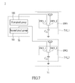
The image sensor includes an image sensing array. The image sensing array includes a plurality of pixel units for capturing image of the illuminated working surface. Please refer to FIG. 1 and FIG. 2. FIG. 1 is schematic diagram illustrating a conventional pixel unit. FIG. 2 is a timing waveform diagram illustrating the operation of the conventional pixel unit.
The pixel unit 15 includes a PMOS transistor MP1, a NMOS transistor MN1, a NMOS transistor MN2, a NMOS transistor MN3, a PMOS transistor MP2, a bipolar junction transistor (hereinafter BJT transistor) Q, a photodetector PD and a capacitor C. The PMOS transistor MP1, the NMOS transistor MN1 and the NMOS transistor MN2 compose a feedback amplifier circuit 150. The NMOS transistor MN3 and the PMOS transistor MP2 compose a shutter circuit 151. The feedback amplifier circuit 150, the shutter circuit 151 and the photodetector PD are respectively coupled to the BJT transistor Q. The capacitor C is coupled to the shutter circuit 151 and the ground. The capacitor C is configured for operatively storing the image data captured by the photodetector PD.
The operation of the pixel unit 15 can be briefly described as follow. At start of each frame, a light-emitting diode (not shown in FIG. 1) provides a light beam to illuminate the working surface, and the working surface reflects the light beam and generates a reflected light beam. The photodetector PD operatively generates a base current IB in responsive to a light intensity of the reflected light. The feedback amplifier circuit 150 begins to build up a base-emitter voltage VBE of the BJT transistor Q to increase the beta of the BJT transistor Q to a stable state e.g., ˜30. The beta herein is the ratio between the collector current IC and the base current IB of the BJT transistor Q. When the BJT transistor Q reaches the stable state, the BJT transistor Q operates with a stable beta and generates a stable emitter current IE. Next, the shutter circuit 151 is triggered on by a shutter signal such that the storage capacitor C can be discharged with a stable emitter current IE to capture the image data. Accordingly, when the shutter circuit 151 is triggered on, the voltage across the capacitor C decreases as the capacitor C discharges through BJT transistor Q with the emitter current IE.
The time required from the light-emitting diode turning on (the base-emitter voltage VBE of the BJT transistor Q starts to increase) to the time the BJT transistor Q reaching the stable state is defined as the pre-flash time of the BJT pixel circuit Q. The time required from the shutter circuit being triggered on until the completion of image capturing is defined as an exposure time. In a conventional image sensor, the pre-flash time is set to about 220 microseconds (us), and the exposure time is set to about 10 us.
However, there is a problem in the conventional image sensor. According to brightness of the image data, the pre-flash time required by the pixel unit 15 will be different. In order to achieve high image quality, the darker image data needs enough pre-flash time. In other words, the darker the image data is, the longer the pre-flash time is required. However, the brighter image does not need too long pre-flash time. Because the conventional image sensor fixes the pre-flash time, when the pixel unit 15 captures the brighter image data, the pre-flash time does not end as soon as the base-emitter voltage VBE of the BJT transistor Q reaches the stable state. The light-emitting unit will waste power if the image sensor operates with the fixed pre-flash time.
SUMMARY
An exemplary embodiment of the present disclosure provides a pre-flash time adjusting circuit which comprises a first pre-flash time adjusting unit coupled to an image sensing array. The image sensing array comprises a plurality of pixel units. The first pre-flash time adjusting unit comprises a switching module and a storage capacitor. A first switch of the switching module is coupled to a first pixel group of the image sensing array, and a second switch of the switching module is coupled to a voltage source. A first end of the storage capacitor is coupled to the switching module, and a second end of the storage capacitor is coupled to ground. The first pixel group comprises a plurality of first pixel units of the pixel units. When the image sensing array senses a light beam, the switching module selectively connects the first switch and the storage capacitor, such that the storage capacitor starts to charge the first pixel units of the first pixel group, until base-emitter voltages of a plurality of bipolar junction transistors disposed in the first pixel units reaches a stable state.
An exemplary embodiment of the present disclosure provides an image sensor. The image sensor comprises an image sensing array and a pre-flash time adjusting circuit. The image sensing array comprises a plurality of pixel units. The pre-flash time adjusting circuit comprises a first pre-flash time adjusting unit coupled to the image sensing array. The first pre-flash time adjusting unit comprises a switching module and a storage capacitor. A first switch of the switching module is coupled to a first pixel group of the image sensing array, and a second switch of the switching module is coupled to a voltage source. A first end of the storage capacitor is coupled to a third end of the switching module, and a second end of the storage capacitor is coupled to ground. The first pixel group comprises a plurality of first pixel units of the pixel units. When the image sensing array senses a light beam, the switching module selectively connects the first switch and the storage capacitor, such that the storage capacitor starts to charge the first pixel units of the first pixel group, until base-emitter voltages of a plurality of bipolar junction transistors disposed in the first pixel units reach a stable state.
To sum up, the pre-flash time adjusting circuit and the image sensor provided by the present disclosure can adaptively adjust the pre-flash time of the pixel units of the image sensing array in response to the brightness of the image data associated with the working surface, and adjust working duration of the light-emitting unit disposed in the image sensor. Compared with the conventional image sensor which fixes the pre-flash time, the pre-flash time adjusting circuit and the image sensor provided by the present disclosure reduces power consumption of the light-emitting unit effectively.
In order to further understand the techniques, means and effects of the present disclosure, the following detailed descriptions and appended drawings are hereby referred to, such that, and through which, the purposes, features and aspects of the present disclosure can be thoroughly and concretely appreciated; however, the appended drawings are merely provided for reference and illustration, without any intention to be used for limiting the present disclosure.
BRIEF DESCRIPTION OF THE DRAWINGS
The accompanying drawings are included to provide a further understanding of the present disclosure, and are incorporated in and constitute a part of this specification. The drawings illustrate exemplary embodiments of the present disclosure and, together with the description, serve to explain the principles of the present disclosure.
FIG. 1 is schematic diagram illustrating a conventional pixel unit.
FIG. 2 is a timing waveform diagram illustrating the operation of the conventional pixel unit.
FIG. 3 is a schematic diagram illustrating an image sensor provided in accordance to an exemplary embodiment of the present disclosure.
FIG. 4 is a circuit diagram illustrating the image sensor provided in accordance to an exemplary embodiment of the present disclosure.
FIG. 5 is a timing waveform diagram illustrating the operation of the image sensor.
FIG. 6 is a schematic diagram illustrating an image sensor provided in accordance to another exemplary embodiment of the present disclosure.
FIG. 7 is a schematic diagram illustrating an image sensor provided in accordance to another exemplary embodiment of the present disclosure.
DESCRIPTION OF THE EXEMPLARY EMBODIMENTS
Reference will now be made in detail to the exemplary embodiments of the present disclosure, examples of which are illustrated in the accompanying drawings. Wherever possible, the same reference numbers are used in the drawings and the description to refer to the same or like parts.
Notably, the terms first, second, third, etc., may be used herein to describe various elements or signals, but these signals should not be affected by such elements or terms. Such terminology is used to distinguish one element from another or a signal with another signal. Further, the term “or” as used herein in the case may include any one or combinations of the associated listed items.
Please refer to FIG. 3, which shows a schematic diagram illustrating an image sensor provided in accordance to an exemplary embodiment of the present disclosure. The image sensor 3 is used in an optical navigation device (not shown in FIG. 3) which operates on a working surface. The optical navigation device comprises a light-emitting unit LED (not shown in FIG. 3), such as a light-emitting unit diode or a laser diode. The light-emitting unit LED is configured for operatively providing a light beam illuminating the working surface, such that the image sensor 3 can capture image data of the illuminated working surface. In the instant embodiment, the optical navigation device may include but is not limited to an optical mouse, a track pad, or a joystick. The image sensor 3 includes an image sensing array 30 and a pre-flash time adjusting circuit 31. The image sensing array 30 is coupled to the pre-flash time adjusting circuit 31.
The image sensing array 30 includes suitable logic, circuit and/or coding, configured for operatively capturing the image data of the working surface. To put it concretely, the image sensing array 30 includes a plurality of pixel units (not shown in FIG. 3) forming at least one pixel group. The pixel units are configured for operatively receiving a light beam and capturing the image data associated with the working surface. In the exemplary embodiment, the image sensing array 30 includes only one pixel group.
The image sensing array 30 is a complementary metal-oxide semiconductor (CMOS) image sensing array, or a charge-coupled device (CCD) image sensing array. However, the present disclosure is not limited thereto.
The pre-flash time adjusting circuit 31 includes at least one pre-flash time adjusting unit 310. The pre-flash time adjusting unit 310 includes a switching module SW and a storage capacitor CS. A first switch SW_1 of the switching module SW is coupled to the image sensing array 30. A second switch SW_2 of the switching module SW is coupled to a voltage source to receive a supply voltage VDD. The switching module SW is coupled to a first end of the storage capacitor CS. A second end of the storage capacitor CS is coupled to a ground. The switching module SW is configured for selectively connecting the first switch SW_1 and the storage capacitor CS, or selectively connecting the second switch SW_2 and the storage capacitor CS.
The pre-flash time adjusting circuit 31 adaptively adjusts a pre-flash time of the image sensing array 30, such that the image sensing array 30 captures the corresponding image data. By disposing the pre-flash time adjusting circuit 31 in the image sensing array 30, the light-emitting unit LED can reduce power consumption.
To explain a structure and an operation of the image sensor 3, please refer to FIG. 4, which shows a circuit diagram illustrating the image sensor provided in accordance to an exemplary embodiment of the present disclosure. As described above, the image sensor 3 comprises an image sensing array 30 and a pre-flash time adjusting circuit 31. The image sensing array 30 comprises a pixel group 300 which includes N pixel units connected in parallel, wherein N is a positive integer greater than 1.
A first pixel unit of the pixel units includes a PMOS transistor MP1_1, a NMOS transistor MN1_1, a NMOS transistor MN2_1, a NMOS transistor MN3_1, a PMOS transistor MP2_1, a BJT transistor Q1, a photodetector PD1 and a first capacitor C1. The BJT transistor Q1 in the instant embodiment is a PNP bipolar junction transistor. The PMOS transistor MP1_1, the NMOS transistor MN1_1 and the NMOS transistor MN2_1 compose a feedback amplifier circuit. The NMOS transistor MN3_1 and PMOS transistor MP2_1 compose a shutter circuit.
A source of the PMOS transistor MP1_1 is coupled to the voltage source to receive the supply voltage VDD. A gate of the PMOS transistor MP1_1 is coupled to a bias end to receive a bias voltage VBIAS. A drain of the PMOS transistor MP1_1 is coupled to a drain of the NMOS transistor MN2_1. A gate of the NMOS transistor MN2_1 is coupled to a base of the BJT transistor Q1. A source of the NMOS transistor MN2_1 is coupled to the ground. A gate of the NMOS transistor MN1_1 is coupled to a drain of the PMOS transistor MP1_1. A drain of the NMOS transistor MN1_1 is coupled to a source of the NMOS transistor MN3_1. A source of the NMOS transistor MN1_1 is coupled to an emitter of the BJT transistor Q1.
A drain of the NMOS transistor MN3_1 is coupled to a control end to receive a control voltage VRST1. Moreover, the drain of the NMOS transistor MN3_1 is further coupled to the first switch SW_1 of the switching module SW. A gate of the NMOS transistor MN3_1 is coupled to a gate of the PMOS transistor MP2_1. The drain of the PMOS transistor MP2_1 is coupled to a source of the NMOS transistor MN3_1. A gate of the PMOS transistor MP2_1 is coupled to a shutter end to receive a shutter signal SHUTTER. A source of the PMOS transistor MP2_1 is coupled to a first end of the first capacitor C1. A collector of the BJT transistor Q1 and a second end of the first capacitor C1 are coupled to the ground. Additionally, a control circuit (not shown in FIG. 4) is respectively coupled to the bias end, the control end, and the shutter end to control the operation of the image sensing array 30.
A cathode of the photodetector PD1 is coupled to a base of the BJT transistor Q1. An anode of the photodetector PD1 is coupled to the ground. The cathode of the photodetector PD1 is further coupled to the base of the BJT transistor Q1. In other words, the photodetector PD1 is coupled between the base of the BJT transistor Q1 and the ground. The photodetector PD1 may be implemented by a photodiode, however in practice, the photodetector PD1 may be any light sensing element or circuit that transforms light intensity into a voltage value and the present disclosure is not limited thereto.
Structures of other pixel units included in the pixel group 300 are similar to the first pixel unit, thus their description is omitted. Incidentally, the structures of the pixel units described above are not limited to the examples provided by the instant embodiment. The pixel units may be any circuits that can capture the image data and the present disclosure is not limited thereto.
The pre-flash time adjusting circuit 31 comprises a pre-flash time adjusting unit 310 and a comparator 311. The structure and the connection of the pre-flash time adjusting unit 310 are as described previously. A non-inverting input end of the comparator 311 is coupled to the first end of the storage capacitor CS, and an inverting input end of the comparator 311 receives a threshold voltage VTH.
At the start of each frame, the first switch SW_1 of the switching module SW connects to the storage capacitor CS, and the storage capacitor CS starts providing a charge current IETOL to the pixel units. A current value of the charge current IETOL is associated with emitter currents of the BJT transistors Q1 . . . Qn of the pixel units. In a mathematical formula, the charge current IETOL=IE1+IE2+ . . . IEn, wherein IE1 is the emitter current of the BJT transistors Q1, IE2 is the emitter current of the BJT transistors Q2, and IEn is the emitter current of the BJT transistors Qn.
To explain the operation of the image sensor 3, please refer to FIG. 5, which shows a timing waveform diagram illustrating the operation of the image sensor. At the start of each frame, the control circuit turns on the light-emitting unit LED to illuminate the working surface of the optical navigation device. Meanwhile, the photodetector PD1 operatively generates a base current IB1 based on the light intensity of a reflected light beam incident on the photodetector PD1, wherein the reflected light beam is the light reflected from the working surface illuminated by the light-emitting unit LED.
The control circuit outputs a first switching signal S1 with a logic high level to the switching module SW, such that the switching module SW connects the first switch SW_1 and the storage capacitor CS. At this time, the second switch SW_2 and storage capacitor CS are electrically isolated.
Next, the storage capacitor CS starts providing the charge current IETOL to charge the pixel units. For the first pixel unit, the PMOS transistor MP1_1, the NMOS transistor MN1_1 and the NMOS transistor MN2_1 of the first pixel unit continues to operatively increase the base-emitter voltage VBE of the BJT transistor Q1 so as to increase the beta of the BJT transistor Q1 to a stable state (e.g., ˜30) after the first pixel unit receives the charge current IETOL through the NMOS transistor MN3_1. The beta herein is the ratio between the collector current IC1 and the base current IB1 of the BJT transistor Q1. When the BJT transistor Q1 reaches the stable state, the BJT transistor Q1 operates with a stable base-emitter voltage VBE and generates a stable emitter current IE1.
Similarly, the base-emitter voltages VBE of the BJT transistor Q2-Qn disposed in the second pixel unit to the N-th pixel unit respectively increase to reach the stable state. The pre-flash time is defined as a period from when the base-emitter voltages VBE of the BJT transistors disposed in the pixel units begin to rise until the stable state.
Electric charge quantity stored in the storage capacitor CS decreases along with time because the storage capacitor CS continues to operatively provide the charge current IETOL to the pixel units, which means that a voltage level VC of the first end of the storage capacitor CS will decrease along with time. In other words, the voltage level VC of the first end of the storage capacitor CS is associated with the base-emitter voltages VBE of the pixel units. Before the voltage level VC of the first end of the storage capacitor CS is less than a threshold voltage VTH, the comparator 311 outputs a comparative signal Vo with a logic high level to the control circuit.
Until all of the base-emitter voltages VBE of the pixel units reach the stable state, the voltage level VC of the first end of the storage capacitor CS is less than a threshold voltage VTH. Then, the comparator 311 outputs the comparative signal Vo with a logic low level to the control circuit.
After sensing the logic level of the comparative signal Vo changes from high to low, the control circuit outputs the first switching signal S1 with a logic low level to the switching module SW. The switching module SW electrically isolates the first switch SW_1 and the storage capacitor CS to finish the pre-flash time of the pixel units. Moreover, the control circuit outputs a second switching signal S2 with a logic high level to the switching module SW. The switching module SW connects the second switch SW_2 and the storage capacitor CS, and then the voltage level VC of the first end of the storage capacitor CS is reset to an initial voltage.
On the other hand, the control circuit outputs shutter signals SHUTTER with logic low level to the shutter ends of each pixel unit to begin the exposure time of the photodetectors PD1 . . . PDn. The PMOS transistors MP2_1 . . . MP2_n are turning on and the NMOS transistors MN3_1 . . . MN3_n are turning off During the exposure time, the first capacitor C1 to the n-th capacitor Cn of the pixel units stably discharge through the BJT transistor Q1 . . . Qn with the emitter current IE1 . . . IEn. Then, the pixel units capture the image data associated with the working surface.
In FIG. 5, there is a gap time between the pre-flash time and the exposure time. During the gap time, the control circuit receives the comparative signal Vo outputted by the comparator 311, and then outputs the first switching signal S1, the second switching signal S2 and the shutter signal SHUTTER in response to the comparative signal Vo. The present disclosure does not limit the duration of the gap time. In the current exemplary embodiment, the gap time is close to zero.
In summary, the pre-flash time adjusting circuit 31 provided by the present disclosure can adaptively adjust the pre-flash time of the pixel units based upon the brightness of the image data. The darker the image data is, the more the pre-flash time adjusting circuit 31 increases the pre-flash time through the switching module SW. On the contrary, The brighter the image data is, the more the pre-flash time adjusting circuit 31 decreases the pre-flash time through the switching module SW. Accordingly, the light-emitting unit LED stops providing the light beam after the base-emitter voltages VBE of the BJT transistors Q1 . . . Qn reach the stable state to save power.
For instance, when the image sensing array 30 captures the brighter image data, the BJT transistors Q1 . . . Qn may need only 30 us to reach the stable state. Then, the light-emitting unit LED turns on for 30 us to provide the light beam. Compared with the conventional image sensor which sets a fixed pre-flash time (e.g., 220 us), the image sensor 3 provided by the present disclosure can save 86% of the power consumed by the light-emitting unit LED.
Incidentally, duration of the exposure time is associated with duration of the pre-flash time, which means that the duration of the exposure time will vary in response to the brightness of the image data. The longer the pre-flash time is, the longer the exposure time needed for the pixel units to capture the image data.
When one of the pixel units (such as the N-th pixel unit) is damaged and unable to accurately capture the image data, the control circuit stops providing current to the N-th pixel unit to save power.
Please refer to FIG. 6, which shows a schematic diagram illustrating an image sensor provided in accordance to another exemplary embodiment of the present disclosure. A structure of the image sensor 6 shown in FIG. 6 is similar to the image sensor 3 shown in FIG. 3, and therefore only differences between them will be described below.
The image sensor 6 also comprises an image sensing array 60 and a pre-flash time adjusting circuit 61. Differences between the image sensor 3 and the image sensor 6 are that, a switching module SW′ of a pre-flash time adjusting unit 610 of the pre-flash time adjusting circuit 61 further comprises a third switch SW_3′ besides a first switch SW_1′ and a second switch SW_2′. Furthermore, the image sensing array 60 is divided into a first pixel group 600 and a second pixel group 601. The first pixel group 600 and the second pixel group 601 respectively include a plurality of pixel units.
The first switch SW_1′ of the switching module SW′ is coupled to the first pixel group 600. The second switch SW_2′ of the switching module SW′ is coupled to a voltage source to receive a supply voltage VDD. The switching module SW′ is coupled to a first end of the storage capacitor CS′. A second end of the storage capacitor CS′ is coupled to a ground. The third switch SW_3′ of the switching module SW′ is coupled to the second pixel group 601.
Operation of the pre-flash time adjusting circuit 61 is similar to the pre-flash time adjusting circuit 31 described above. When the image sensor 6 wants to capture an image data through the first pixel group 600, a control circuit (not shown in FIG. 6) outputs a first switching signal S1′, such that the switching module SW′ connects the first switch SW_1′ and the storage capacitor CS′. The storage capacitor CS′ starts providing a charge current to charge the pixel units of the first pixel group 600. The pre-flash time adjusting unit 610 correspondingly adjusts a first pre-flash time of the first pixel group 600 in response to brightness of the image data.
When all of the BJT transistors (not shown in FIG. 6) disposed in the first pixel group 600 reach a stable state, the switching module SW′ connects the second switch SW_2′ and the storage capacitor CS′, and the first switch SW_1′ and the storage capacitor CS′ is electrically isolated. Electric charge quantity stored in the storage capacitor CS′ is reset. Then, the first pixel group 600 begins an exposure time to capture the image data.
Or, when the image sensor 6 wants to capture the image data through the second pixel group 601, the control circuit outputs a third switching signal S3′, such that the switching module SW′ connects the third switch SW_3′ and the storage capacitor CS′. The storage capacitor CS′ starts providing the charge current to charge the pixel units of the second pixel group 601. The pre-flash time adjusting unit 610 correspondingly adjusts a second pre-flash time of the second pixel group 601 in response to brightness of the image data.
The pixel units of the first pixel group 600 are controlled by the first switch SW_1′ of the switching module SW′, and the pixel units of the second pixel group 601 are controlled by the third switch SW_3′ of the switching module SW′. In terms of the switching module SW′, the pixel units of the first pixel group 600 have the same first pre-flash time, and the pixel units of the second pixel group 601 have the same second pre-flash time. According to the brightness of the image data, the first pre-flash time may equal to the second pre-flash time, or the first pre-flash time may different to the second pre-flash time.
Depending on the application of the image sensor 6, the pre-flash time adjusting circuit 61 can simultaneously provide the charge current to the first pixel group 600 and the second pixel group 601, or the pre-flash time adjusting circuit 61 can alternately provide the charge current to the first pixel group 600 and the second pixel group 601.
Notably, in the current exemplary embodiment, the image sensing array 60 is divided into two pixel groups. However, the present disclosure is not limited thereto. In another exemplary embodiment, the image sensing array 60 can be divided into M pixel groups, wherein M is a positive integer greater than 1. The switching module SW′ increases the number of pins according to the number of the pixel groups to adaptively adjust the pre-flash time of the pixel groups.
Please refer to FIG. 7, which shows a schematic diagram illustrating an image sensor provided in accordance to another exemplary embodiment of the present disclosure. A structure of the image sensor 7 shown in FIG. 7 is similar to the image sensor 3 shown in FIG. 3 and the image sensor 6 shown in FIG. 6, and therefore only differences between them will be described below.
The image sensor 7 also comprises an image sensing array 70 and a pre-flash time adjusting circuit 71. The difference between the image sensors 3 and 6 and the image sensor 7 is that, the pre-flash time adjusting circuit 71 includes a first pre-flash time adjusting unit 710_1 and a second pre-flash time adjusting unit 710_2. Furthermore, the image sensing array 70 is divided into a first pixel group 700 and a second pixel group 701. The first pixel group 700 and the second pixel group 701 respectively include a plurality of pixel units.
The first pre-flash time adjusting unit 710_1 includes a switching module SW1 comprising a first switch SW1_1 and second switch SW1_2. The first switch SW1_1 of the switching module SW1 is coupled to the first pixel group 700. The second switch SW1_2 of the switching module SW1 is coupled to a voltage source to receive a supply voltage VDD. The switching module SW1 is coupled to a first end of the storage capacitor CS1. A second end of the storage capacitor CS1 is coupled to a ground.
Operation of the first pre-flash time adjusting unit 710_1 is similar to the pre-flash time adjusting unit 310 described above, further descriptions are hereby omitted. The pre-flash time adjusting circuit 71 correspondingly adjusts a first pre-flash time of the first pixel group 700 through the first pre-flash time adjusting unit 710_1.
On the other hand, the second pre-flash time adjusting unit 710_2 includes a switching module SW2 comprising a first switch SW2_1 and second switch SW2_2. The first switch SW2_1 of the switching module SW2 is coupled to the second pixel group 701. The second switch SW2_2 of the switching module SW2 is coupled to a voltage source to receive a supply voltage VDD. The switching module SW2 is coupled to a first end of the storage capacitor CS2. A second end of the storage capacitor CS2 is coupled to the ground.
Operation of the second pre-flash time adjusting unit 710_2 is similar to the pre-flash time adjusting unit 310 described above, further descriptions are hereby omitted. The pre-flash time adjusting circuit 71 correspondingly adjusts a second pre-flash time of the second pixel group 701 through the second pre-flash time adjusting unit 710_2.
The first pre-flash time adjusting unit 710_1 and the second pre-flash time adjusting unit 710_2 are each independent from each other. Depending on the application of the image sensor 7, the pre-flash time adjusting circuit 71 can simultaneously provide a charge current to the first pixel group 700 and the second pixel group 701, or the pre-flash time adjusting circuit 71 can alternately provide the charge current to the first pixel group 700 and the second pixel group 701. Moreover, depending on brightness of an image data captured by the image sensing array 70, the first pre-flash time of the first pixel group 700 may be different from the second pre-flash time of the second pixel group 701, or the first pre-flash time of the first pixel group 700 may equal to the second pre-flash time of the second pixel group 701.
Notably, in the current exemplary embodiment, the pre-flash time adjusting circuit 71 only includes the first pre-flash time adjusting unit 710_1 and the second pre-flash time adjusting unit 710_2. However, the present disclosure is not limited thereto. In another exemplary embodiment, the pre-flash time adjusting circuit 71 can include X pre-flash time adjusting units, wherein X is a positive integer greater than 1. The image sensing array 70 is divided into X pixel groups according to a number of the pre-flash time adjusting units. Hence, the pre-flash time adjusting circuit 71 can adaptively adjust the pre-flash time of the pixel groups.
In summary, the pre-flash time adjusting circuit and the image sensor provided by the present disclosure can adaptively adjust the pre-flash time of the pixel units of the image sensing array in response to the brightness of the image data associated with the working surface, and adjust working duration of the light-emitting unit disposed in the image sensor. Compared with the conventional image sensor which fixes the pre-flash time, the pre-flash time adjusting circuit and the image sensor provided by the present disclosure reduces power consumption of the light-emitting unit effectively.
The above-mentioned descriptions represent merely the exemplary embodiment of the present disclosure, without any intention to limit the scope of the present disclosure thereto. Various equivalent changes, alterations or modifications based on the claims of present disclosure are all consequently viewed as being embraced by the scope of the present disclosure.

Claims (20)

What is claimed is:
1. A pre-flash time adjusting circuit which comprises a first pre-flash time adjusting unit coupled to an image sensing array, wherein the image sensing array comprises a plurality of pixel units, and the first pre-flash time adjusting unit comprises:
a switching module, wherein a first switch of the switching module is coupled to a first pixel group of the image sensing array, and a second switch of the switching module is coupled to a voltage source, wherein the first pixel group comprises a plurality of first pixel units of the pixel units; and
a storage capacitor, wherein a first end of the storage capacitor is coupled to the switching module, and a second end of the storage capacitor is coupled to a ground;
wherein when the image sensing array senses a light beam, the switching module selectively connects the first switch and the storage capacitor, such that the storage capacitor starts to charge the first pixel units of the first pixel group, until base-emitter voltages of a plurality of bipolar junction transistors disposed in the first pixel units reaches a stable state.
2. The pre-flash time adjusting circuit according to claim 1, wherein a first pre-flash time is defined as a period from when the base-emitter voltages of the bipolar junction transistors disposed in the first pixel units begin to rise until the stable state.
3. The pre-flash time adjusting circuit according to claim 1, wherein when the switching module selectively connects the first switch and the storage capacitor, the second switch and the storage capacitor is electrically isolated.
4. The pre-flash time adjusting circuit according to claim 1, wherein the first end of the storage capacitor is further coupled to a non-inverting input end of a comparator, and an inverting input end of the comparator receives a threshold voltage, when a voltage level of the first end of the storage capacitor is higher than the threshold voltage, the comparator outputs a comparative signal with a logic high level; wherein the voltage level of the first end of the storage capacitor is associated with the base-emitter voltages of the first pixel units of the first pixel group.
5. The pre-flash time adjusting circuit according to claim 4, wherein electric charge quantity stored in the storage capacitor decreases along with time, such that the voltage level of the first end of the storage capacitor decreases, and then the base-emitter voltages of the first pixel units of the first pixel group increases, until the voltage level of the first end of the storage capacitor is less than the threshold voltage, the comparator outputs the comparative signal with a logic low level to finish the pre-flash time of the first pixel units.
6. The pre-flash time adjusting circuit according to claim 5, wherein when the comparator outputs the comparative signal with the logic low level, a control circuit outputs a switching signal to the pre-flash time adjusting unit, such that the first switch and the storage capacitor is electrically isolated, and the second switch and the storage capacitor is electrically connected, and then the voltage level of the first end of the storage capacitor is reset to an initial voltage.
7. The pre-flash time adjusting circuit according to claim 5, wherein when the comparator outputs the comparative signal with the logic low level, a control circuit outputs a shutter signal to the image sensing array, such that the pixel units captures an image data.
8. The pre-flash time adjusting circuit according to claim 1, wherein the switching module further comprises:
a third switch, coupled to a second pixel group of the image sensing array, wherein the second pixel group comprises a plurality of second pixel units of the pixel units;
wherein the pre-flash time adjusting unit selectively connects the storage capacitor and the third switch based upon a switching signal, such that the storage capacitor starts to charge the second pixel units of the second pixel group, until base-emitter voltages of a plurality of bipolar junction transistors disposed in the second pixel units reaches the stable state.
9. The pre-flash time adjusting circuit according to claim 1, further comprising:
a second pre-flash time adjusting unit, coupled to a second pixel group of the image sensing array, wherein the second pixel group comprises a plurality of second pixel units of the pixel units;
wherein the first pixel units of the first pixel group have the same first pre-flash time, and the second pixel units of the second pixel group have the same second pre-flash time.
10. The pre-flash time adjusting circuit according to claim 1, wherein the image sensing array is a complementary metal-oxide semiconductor (CMOS) image sensing array, or a charge-coupled device (CCD) image sensing array.
11. An image sensor, comprising:
an image sensing array, comprising a plurality of pixel units; and
a pre-flash time adjusting circuit, comprising a first pre-flash time adjusting unit coupled to the image sensing array, wherein the first pre-flash time adjusting unit comprises:
a switching module, wherein a first switch of the switching module is coupled to a first pixel group of the image sensing array, and a second switch of the switching module is coupled to a voltage source, wherein the first pixel group comprises a plurality of first pixel units of the pixel units; and
a storage capacitor, wherein a first end of the storage capacitor is coupled to the switching module, and a second end of the storage capacitor is coupled to a ground;
wherein when the image sensing array senses a light beam, the switching module selectively connects the first switch and the storage capacitor, such that the storage capacitor starts to charge the first pixel units of the first pixel group, until base-emitter voltages of a plurality of bipolar junction transistors disposed in the first pixel units reaches a stable state.
12. The image sensor according to claim 11, wherein a first pre-flash time is defined as a period from when the base-emitter voltages of the bipolar junction transistors disposed in the first pixel units begin to rise until the stable state.
13. The image sensor according to claim 11, wherein when switching module selectively connects the first switch and the storage capacitor, the second switch and the storage capacitor is electrically isolated.
14. The image sensor according to claim 11, wherein the first end of the storage capacitor is further coupled to a non-inverting input end of a comparator, and an inverting input end of the comparator receives a threshold voltage, when a voltage level of the first end of the storage capacitor is higher than the threshold voltage, the comparator outputs a comparative signal with a logic high level; wherein the voltage level of the first end of the storage capacitor is associated with the base-emitter voltages of the first pixel units of the first pixel group.
15. The image sensor according to claim 14, wherein electric charge quantity stored in the storage capacitor decreases along with time, such that the voltage level of the first end of the storage capacitor decreases, and then the base-emitter voltages of the first pixel units of the first pixel group increases, until the voltage level of the first end of the storage capacitor is less than the threshold voltage, the comparator outputs the comparative signal with a logic low level to finish pre-flash of the first pixel units.
16. The image sensor according to claim 15, wherein when the comparator outputs the comparative signal with the logic low level, a control circuit outputs a switching signal to the pre-flash time adjusting unit, such that the first switch and the storage capacitor is electrically isolated, and the second switch and the storage capacitor is connected, and then the voltage level of the first end of the storage capacitor is reset to an initial voltage.
17. The image sensor according to claim 15, wherein when the comparator outputs the comparative signal with the logic low level, a control circuit outputs a shutter signal to the image sensing array, such that the pixel units captures an image data.
18. The image sensor according to claim 11, wherein the switching module further comprises:
a third switch, coupled to a second pixel group of the image sensing array, wherein the second pixel group comprises a plurality of second pixel units of the pixel units;
wherein the pre-flash time adjusting unit selectively connects the storage capacitor and the third switch based upon a switching signal, such that the storage capacitor starts to charge the second pixel units of the second pixel group, until base-emitter voltages of a plurality of bipolar junction transistors disposed in the second pixel units reaches the stable state.
19. The image sensor according to claim 11, wherein the pre-flash time adjusting circuit further comprises:
a second pre-flash time adjusting unit, coupled to a second pixel group of the image sensing array, wherein the second pixel group comprises a plurality of second pixel units of the pixel units;
wherein the first pixel units of the first pixel group have the same first pre-flash time, and the second pixel units of the second pixel group have the same second pre-flash time.
20. The image sensor according to claim 11, wherein the image sensing array is a complementary metal-oxide semiconductor (CMOS) image sensing array, or a charge-coupled device (CCD) image sensing array.
US14/873,607 2015-10-02 2015-10-02 Pre-flash time adjusting circuit and image sensor using the same Active US9412784B1 (en)

Priority Applications (3)

Application Number Priority Date Filing Date Title
US14/873,607 US9412784B1 (en) 2015-10-02 2015-10-02 Pre-flash time adjusting circuit and image sensor using the same
TW104144448A TWI544746B (en) 2015-10-02 2015-12-30 Pre-flash time adjustment circuit and image sensor using the same
CN201610028513.2A CN106561048B (en) 2015-10-02 2016-01-15 Pre-flash time adjusting circuit and image sensor using same

Applications Claiming Priority (1)

Application Number Priority Date Filing Date Title
US14/873,607 US9412784B1 (en) 2015-10-02 2015-10-02 Pre-flash time adjusting circuit and image sensor using the same

Publications (1)

Publication Number Publication Date
US9412784B1 true US9412784B1 (en) 2016-08-09

Family

ID=56556454

Family Applications (1)

Application Number Title Priority Date Filing Date
US14/873,607 Active US9412784B1 (en) 2015-10-02 2015-10-02 Pre-flash time adjusting circuit and image sensor using the same

Country Status (3)

Country Link
US (1) US9412784B1 (en)
CN (1) CN106561048B (en)
TW (1) TWI544746B (en)

Cited By (3)

* Cited by examiner, † Cited by third party
Publication number Priority date Publication date Assignee Title
US20170277278A1 (en) * 2016-03-22 2017-09-28 Pixart Imaging (Penang) Sdn. Bhd. Circuit and method for detecting working and resting states for optical mouse
US10431623B2 (en) * 2017-10-22 2019-10-01 Pixart Imaging Inc. Method applied to BJT pixel of image sensor apparatus and image sensor apparatus
US12432470B2 (en) * 2023-12-14 2025-09-30 Pixart Imaging Inc. Mechanism of effectively shortening settling time of pixel circuit

Citations (5)

* Cited by examiner, † Cited by third party
Publication number Priority date Publication date Assignee Title
US20010054744A1 (en) * 2000-01-21 2001-12-27 John Scott-Thomas Analog storage for a CMOS array
US20050253812A1 (en) * 2004-05-12 2005-11-17 Sunplus Technology Co., Ltd. Optical mouse with shade compensation and its shade compensation method
US20110291924A1 (en) * 2010-05-25 2011-12-01 Jeffrey Raynor Optical navigation device and associated methods
US20130241442A1 (en) * 2010-09-30 2013-09-19 Ams Ag Method for current limitation of a load current and circuit having current limitation of a load current for a flash means
US20150042566A1 (en) * 2013-08-07 2015-02-12 Pixart Imaging Inc. Bipolar junction transistor pixel circuit, driving method thereof, and image sensor

Family Cites Families (1)

* Cited by examiner, † Cited by third party
Publication number Priority date Publication date Assignee Title
CN100365542C (en) * 2002-11-18 2008-01-30 英群企业股份有限公司 Power-saving method and circuit for converting non-power-saving processor electronic device into power-saving mode

Patent Citations (5)

* Cited by examiner, † Cited by third party
Publication number Priority date Publication date Assignee Title
US20010054744A1 (en) * 2000-01-21 2001-12-27 John Scott-Thomas Analog storage for a CMOS array
US20050253812A1 (en) * 2004-05-12 2005-11-17 Sunplus Technology Co., Ltd. Optical mouse with shade compensation and its shade compensation method
US20110291924A1 (en) * 2010-05-25 2011-12-01 Jeffrey Raynor Optical navigation device and associated methods
US20130241442A1 (en) * 2010-09-30 2013-09-19 Ams Ag Method for current limitation of a load current and circuit having current limitation of a load current for a flash means
US20150042566A1 (en) * 2013-08-07 2015-02-12 Pixart Imaging Inc. Bipolar junction transistor pixel circuit, driving method thereof, and image sensor

Cited By (4)

* Cited by examiner, † Cited by third party
Publication number Priority date Publication date Assignee Title
US20170277278A1 (en) * 2016-03-22 2017-09-28 Pixart Imaging (Penang) Sdn. Bhd. Circuit and method for detecting working and resting states for optical mouse
US9864437B2 (en) * 2016-03-22 2018-01-09 Pixart Imaging (Penang) Sdn. Bhd. Circuit and method for detecting working and resting states for optical mouse
US10431623B2 (en) * 2017-10-22 2019-10-01 Pixart Imaging Inc. Method applied to BJT pixel of image sensor apparatus and image sensor apparatus
US12432470B2 (en) * 2023-12-14 2025-09-30 Pixart Imaging Inc. Mechanism of effectively shortening settling time of pixel circuit

Also Published As

Publication number Publication date
TW201714408A (en) 2017-04-16
TWI544746B (en) 2016-08-01
CN106561048B (en) 2019-07-05
CN106561048A (en) 2017-04-12

Similar Documents

Publication Publication Date Title
US9509927B2 (en) Solid-state imaging device, method of driving the same, signal processing method for the same, and imaging apparatus
US8896733B2 (en) Imaging system with automatic conversion gain selection
KR102276536B1 (en) Light-emitting element drive circuit, display device, and a-d conversion circuit
KR101553427B1 (en) Solid-state imaging device and imaging device
TWI599226B (en) Solid-state image capturing device for signal processing method and electronic device of a solid-state image capturing device
US11240461B2 (en) Operating method of pixel circuit and image system
US9380237B2 (en) Semiconductor integrated circuit, current control method, ad converter, solid-state imaging device, and electronic system
JP5212022B2 (en) Solid-state imaging device, imaging device, pixel driving voltage optimization device, and pixel driving voltage optimization method
KR20160020402A (en) A comparator circuit, an A / D conversion circuit, and a display device
US9843752B2 (en) Solid-state image sensor, driving method thereof, and camera
US8379127B2 (en) Pixel sensor array including comparator and image sensor including the same
CN101102423A (en) Photoelectric conversion circuit and solid-state image sensing device using the same
CN108337457B (en) Image Sensor
JP2000162041A (en) Photo-detection device
US9412784B1 (en) Pre-flash time adjusting circuit and image sensor using the same
US20250260910A1 (en) Image sensor and image-capturing device
KR20060104197A (en) CMOS image sensor with dual interrelated sampling functions
US9774808B2 (en) Driving method for photoelectric conversion apparatus, photoelectric conversion apparatus, and imaging system
US11057579B2 (en) Anti-overexposure circuit structure and electronic device using the same
US20050285017A1 (en) Color sensing circuit employing charge storage device
JPS63272185A (en) Photoelectric converter for focus detection
US20230155596A1 (en) Analog-to-digital converting circuit using auto-zero period optimization and operation method thereof
KR20240169393A (en) Image sensor

Legal Events

Date Code Title Description
AS Assignment

Owner name: PIXART IMAGING (PENANG) SDN. BHD., MALAYSIA

Free format text: ASSIGNMENT OF ASSIGNORS INTEREST;ASSIGNOR:LIM, WOOI-KIP;REEL/FRAME:036716/0504

Effective date: 20150304

STCF Information on status: patent grant

Free format text: PATENTED CASE

FEPP Fee payment procedure

Free format text: ENTITY STATUS SET TO UNDISCOUNTED (ORIGINAL EVENT CODE: BIG.); ENTITY STATUS OF PATENT OWNER: LARGE ENTITY

MAFP Maintenance fee payment

Free format text: PAYMENT OF MAINTENANCE FEE, 4TH YEAR, LARGE ENTITY (ORIGINAL EVENT CODE: M1551); ENTITY STATUS OF PATENT OWNER: LARGE ENTITY

Year of fee payment: 4

MAFP Maintenance fee payment

Free format text: PAYMENT OF MAINTENANCE FEE, 8TH YEAR, LARGE ENTITY (ORIGINAL EVENT CODE: M1552); ENTITY STATUS OF PATENT OWNER: LARGE ENTITY

Year of fee payment: 8