US9401619B2 - Charging device - Google Patents
Charging device Download PDFInfo
- Publication number
- US9401619B2 US9401619B2 US14/151,726 US201414151726A US9401619B2 US 9401619 B2 US9401619 B2 US 9401619B2 US 201414151726 A US201414151726 A US 201414151726A US 9401619 B2 US9401619 B2 US 9401619B2
- Authority
- US
- United States
- Prior art keywords
- connection terminal
- electrically connected
- output unit
- power
- power output
- Prior art date
- Legal status (The legal status is an assumption and is not a legal conclusion. Google has not performed a legal analysis and makes no representation as to the accuracy of the status listed.)
- Expired - Fee Related, expires
Links
Images


Classifications
-
- H—ELECTRICITY
- H02—GENERATION; CONVERSION OR DISTRIBUTION OF ELECTRIC POWER
- H02J—ELECTRIC POWER NETWORKS; CIRCUIT ARRANGEMENTS OR SYSTEMS FOR SUPPLYING OR DISTRIBUTING ELECTRIC POWER; SYSTEMS FOR STORING ELECTRIC ENERGY
- H02J7/00—Circuit arrangements for charging or discharging batteries or for supplying loads from batteries
- H02J7/70—Circuit arrangements for charging or discharging batteries or for supplying loads from batteries characterised by the mechanical construction
-
- H02J7/0042—
-
- H—ELECTRICITY
- H02—GENERATION; CONVERSION OR DISTRIBUTION OF ELECTRIC POWER
- H02J—ELECTRIC POWER NETWORKS; CIRCUIT ARRANGEMENTS OR SYSTEMS FOR SUPPLYING OR DISTRIBUTING ELECTRIC POWER; SYSTEMS FOR STORING ELECTRIC ENERGY
- H02J7/00—Circuit arrangements for charging or discharging batteries or for supplying loads from batteries
- H02J7/02—Circuit arrangements for charging or discharging batteries or for supplying loads from batteries for charging batteries from AC mains by converters
-
- H02J7/0031—
-
- H—ELECTRICITY
- H02—GENERATION; CONVERSION OR DISTRIBUTION OF ELECTRIC POWER
- H02J—ELECTRIC POWER NETWORKS; CIRCUIT ARRANGEMENTS OR SYSTEMS FOR SUPPLYING OR DISTRIBUTING ELECTRIC POWER; SYSTEMS FOR STORING ELECTRIC ENERGY
- H02J7/00—Circuit arrangements for charging or discharging batteries or for supplying loads from batteries
- H02J7/60—Circuit arrangements for charging or discharging batteries or for supplying loads from batteries including safety or protection arrangements
- H02J7/663—Circuit arrangements for charging or discharging batteries or for supplying loads from batteries including safety or protection arrangements using battery or load disconnect circuits
-
- H—ELECTRICITY
- H02—GENERATION; CONVERSION OR DISTRIBUTION OF ELECTRIC POWER
- H02J—ELECTRIC POWER NETWORKS; CIRCUIT ARRANGEMENTS OR SYSTEMS FOR SUPPLYING OR DISTRIBUTING ELECTRIC POWER; SYSTEMS FOR STORING ELECTRIC ENERGY
- H02J9/00—Circuit arrangements for emergency or stand-by power supply, e.g. for emergency lighting
- H02J9/005—Circuit arrangements for emergency or stand-by power supply, e.g. for emergency lighting using a power saving mode
Definitions
- the present disclosure relates to a charging device.
- Portable electronic devices such as mobile phones, often have rechargeable batteries for providing operation voltages to the electrical components.
- a portable electronic device is connected to a charging device via a power line and a connector to charge the battery.
- the charging device may keep consuming power, which is wasteful.
- AC alternating current
- FIG. 1 is a schematic view of a first embodiment of a charging device having a power output unit.
- FIG. 2 is a schematic diagram of an internal structure of the power output unit of the charging device of FIG. 1 .
- FIG. 3 is a schematic diagram of the internal structure of the power output unit of FIG. 1 electrically connecting to an electronic device.
- FIG. 4 is a schematic diagram of the internal structure of the power output unit of FIG. 1 after being fully charged.
- FIG. 5 is a schematic diagram of a second embodiment of an internal structure of a power output unit of a charging device disconnected from an electronic device.
- FIG. 6 is a schematic diagram of the internal structure of the power output unit of the charging device of FIG. 5 in a state of being charged.
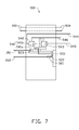
- FIG. 7 is a schematic diagram of a third embodiment of an internal structure of a power output unit of a charging device disconnected from an electronic device.
- FIG. 8 is a schematic diagram of the internal structure of the power output unit of the charging device of FIG. 7 in a state of being charged.
- FIG. 1 shows an embodiment of a charging device 10 .
- the charging device 10 includes a power converting unit 100 , a power output unit 300 , and a plurality of cables 200 connected between the power converting unit 100 and the power output unit 300 .
- the power converting unit 100 converts an alternating current (AC) power from an external power source to a direct current (DC) power, and outputs the DC power to the power output unit 300 via the plurality of cables 200 .
- the power output unit 300 is configured to electrically connect to an electronic device 20 .
- the power output unit 300 outputs the DC power to the electronic device 20 to charge the electronic device 20 .
- the electronic device 20 can be, but is not limited to, a smart phone, a mobile Internet device (MID), or other similar device.
- MID mobile Internet device
- the power converting unit 100 includes a first conductive pin 101 , a second conductive pin 102 , and a converter 110 .
- the first conductive pin 101 and the second conductive pin 102 are electrically connected to the AC power.
- the first conductive pin 101 is electrically connected to the converter 110 .
- the second conductive pin 102 is electrically connected to the power output unit 300 via a first cable 201 .
- the converter 110 includes a first input terminal 111 and a second input terminal 112 .
- the first input terminal 111 is electrically connected to the first conductive pin 101 .
- the second input terminal 112 is electrically connected to the power output unit 300 via a second cable 202 .
- the second input terminal 112 is selectively electrically connected to or disconnected from the second conductive pin 102 under control of the power output unit 300 .
- the converter 110 is electrically connected to the power output unit 300 via the plurality of cables 200 .
- FIG. 2 shows a schematic diagram of an internal structure of the power output unit 300 .
- the power output unit 300 includes a shell 310 , a plurality of electrical pins 330 , and a detection control portion 331 .
- the shell 310 defines a receiving space to receive the plurality of electrical pins 330 and the detection control portion 331 .
- the shell 310 includes a first side surface 311 , a second surface 312 opposite from the first side surface 311 , and a third side surface 313 located between the first side surface 311 and the second surface 312 .
- the plurality of electrical pins 330 and the detection control portion 331 protrude out of the first side surface 311 to connect to the electronic device 20 .
- the plurality of electrical pins 330 are electrically connected to the converter 110 via the plurality of cables 200 .
- the detection control portion 331 detects whether the power output unit 300 is electrically connected to or disconnected from the electronic device 20 and whether the electronic device 20 is fully charged.
- the power output unit 300 further includes a first switch 320 and a second switch 340 received in the receiving space of the shell 310 .
- the first switch 320 is turned on.
- the first switch 320 is turned off.
- the second switch 340 controls the first cable 201 to disconnect from the second cable 202 .
- the second switch 340 controls the first cable 201 to connect to the second cable 202 .
- the first switch 320 includes a first connection terminal 321 , a second connection terminal 322 , a third connection terminal 323 , a fourth connection terminal 324 , a detection bar 325 , a rotation bar 326 , an elastic member 327 , a supporting portion 328 , a pivot 329 , and a platform 350 .
- the platform 350 is located at a substantially middle portion of the third side surface 313 .
- the first connection terminal 321 is fixed on one end portion of the rotation bar 326 and electrically connected to the second conductive pin 102 via the first cable 201 .
- the second connection terminal 322 is aligned with the first connection terminal 321 and fixed on the first side surface 311 .
- the third connection terminal 323 is fixed on the platform 350 and adjacent to the second side surface 312 .
- the third connection terminal 323 is electrically connected to the second input terminal 112 via the second cable 202 .
- the fourth connection terminal 324 is fixed on the platform 350 and located adjacent to the third connection terminal 323 . In one embodiment, the third connection terminal 323 and the fourth connection terminal 324 are located on a same surface of the platform 350 , and the fourth connection terminal 324 is electrically connected to the second connection terminal 322 via the second cable 202 .
- the rotation bar 326 rotates about the pivot 329 .
- a first end of the rotation bar 326 is connected to the second side surface 312 via the elastic member 327 , and a second end of the rotation bar 326 extends toward the fourth connection terminal 324 .
- a first end of the detection bar 325 protrudes out of the first side surface 311 , and a second end of the detection bar 325 resists against the first end of the rotation bar 326 .
- the detection bar 325 and the elastic member 327 are located on two opposite sides of the rotation bar 326 , respectively, and are substantially perpendicular to the rotation bar 326 .
- the supporting portion 328 is located on the second side surface 312 to limit a rotation angle of the rotation bar 326 .
- the second switch 340 includes a substantially T-shaped portion 341 , a first electromagnetic portion 342 , and a second electromagnetic portion 343 .
- the first electromagnetic portion 342 and the second electromagnetic portion 343 are arranged in the shell 310 .
- the first electromagnetic portion 342 and the second electromagnetic portion 343 are magnetized and attract the T-shaped portion 341 .
- the T-shaped portion 341 includes a sliding member 341 a and an attracting member 341 b .
- the sliding member 341 a is slidably connected to the platform 350 .
- the attracting member 341 b is located between the first electromagnetic portion 342 and the second electromagnetic portion 343 .
- the attracting member 341 b is capable of sliding along with the sliding member 341 a .
- the sliding member 341 a is located on and electrically connected between the third connection terminal 323 and the fourth connection terminal 324 .
- the sliding portion 341 a is a conductive element.
- the sliding portion 341 a contacts both the third connection terminal 323 and the fourth connection terminal 324 , thereby electrically connecting the third connection terminal 323 to the fourth connection terminal 324 .
- the sliding portion 341 b slides past the third connection terminal 323 , thereby cutting off the electrical connection between the third connection terminal 323 and the fourth connection terminal 324 .
- the sliding member 341 a is directly fixed on the fourth connection terminal 324 , and the fourth connection terminal 324 is slidable along the platform 350 .
- the sliding member 341 a is electrically connected to the third connection terminal 323 or disconnected from the third connection terminal 323 when the fourth connection terminal 324 slides along the platform 350 .
- the detection control portion 331 includes a first control terminal 344 , a second control terminal 345 , and a third control terminal 346 .
- the first control terminal 344 and the second control terminal 345 are electrically connected to the first electromagnetic portion 342 and the second electromagnetic portion 343 , respectively.
- the third control terminal 346 is electrically connected to both the first electromagnetic portion 342 and the second electromagnetic portion 343 .
- FIGS. 2-4 show different states of the electronic device 20 .
- the rotation bar 326 is substantially perpendicular to the third side surface 313 , the elastic member 327 is not compressed, the first connection terminal 321 is disconnected from the second connection terminal 322 , and the sliding member 341 a is electrically connected between the third connection terminal 323 and the fourth connection terminal 324 .
- the second connection terminal 322 When the first connection terminal 321 is disconnected from the second connection terminal 322 , the second input terminal 112 is disconnected from the second conductive pin 102 . At this time, the second connection terminal 322 , the first connection terminal 321 , the first cable 201 , and the converter 110 stop working.
- the detection bar 325 is pushed into the shell 310 by the electronic device 20 .
- the detection bar 325 pushes the rotation bar 326 to rotate about the pivot 329 , and the elastic member 327 is compressed.
- the rotation bar 326 drives the first connection terminal 321 to electrically connect to the second connection terminal 322 .
- the first control terminal 344 receives a logic high signal (e.g. logic “1”), the second control terminal 345 receives a logic low signal (e.g. logic “0”), and a current flows through the first electromagnetic portion 342 .
- the first electromagnetic portion 342 attracts the T-shaped portion 341 , so the sliding member 341 a is electrically connected between the third connection terminal 323 and the fourth connection terminal 323 a .
- the AC power flows from the external power source to the second input terminal 112 of the converter 110 via the third connection terminal 323 .
- the converter 110 converts the AC power to the DC power.
- the logic high signal and the logic low signal are output by the electronic device 20 .
- the first control terminal 344 receives the logic low signal
- the second control terminal 345 receives the logic high signal
- the current flows through the second control terminal 345 and the third control terminal 346 .
- the second electromagnetic portion 343 attracts the sliding member 341 a , so the sliding member 341 is electrically disconnected from the third connection terminal 323 .
- the converter 110 stops receiving the AC power.
- the detection bar 325 is rebounded out of the shell 310 by the elastic member 327 , and the rotation bar 326 rotates about the pivot 329 .
- the first connection terminal 321 is moved away from the second connection terminal 322 , and the sliding member 341 a is slid toward the third connection terminal 323 .
- the power output unit 300 is reset to the state shown in FIG. 2 .
- FIGS. 5 and 6 show an internal structure of a second embodiment of a power output unit 400 .
- the power output unit 400 is substantially similar to the power output unit 300 , except that the power output unit 400 only includes a first switch 420 .
- a third connection terminal 423 is always electrically connected to a fourth connection terminal 424 .
- FIGS. 7 and 8 show an internal structure of a third embodiment of a power output unit 500 .
- the power output unit 500 is substantially similar to the power output unit 300 , except that the power output unit 500 includes a second switch 540 , a first connection terminal 521 , a second connection terminal 522 , a third connection terminal 523 , and a fourth connection terminal 524 .
- the second switch 540 is substantially the same as the second switch 340 .
- the first connection terminal 521 is fixed on the second connection terminal 522 .
- a first control terminal 544 receives a logic low signal or is floated
- a second control terminal 545 receives a logic high signal
- a current flows through the second control terminal 545 , a second electromagnetic portion 543 , and a third control terminal 546 .
- the second electromagnetic portion 543 attracts an attracting member 541 b .
- the third connection terminal 523 is disconnected from a sliding member 541 a , and the converter 110 stops working.
- the first control terminal 544 receives a logic high signal
- the second control terminal 545 receives a logic low signal.
- a current flows through the first electromagnetic portion 542 , so the first electromagnetic portion attracts the attracting member 541 b .
- the sliding member 541 a is electrically connected between the third connection terminal 523 and the fourth connection terminal 524 .
- the AC power flows to the second input terminal 112 of the converter 110 via the third connection terminal 523 , and the AC power is converted to the DC power.
- the charging device 300 stops receiving the AC power. Therefore, energy is prevented from being wasted.
Landscapes
- Engineering & Computer Science (AREA)
- Power Engineering (AREA)
- Charge And Discharge Circuits For Batteries Or The Like (AREA)
Abstract
Description
Claims (18)
Applications Claiming Priority (3)
| Application Number | Priority Date | Filing Date | Title |
|---|---|---|---|
| TW102200525U | 2013-01-10 | ||
| TW102200525 | 2013-01-10 | ||
| TW102200525U TWM458732U (en) | 2013-01-10 | 2013-01-10 | Charging equipment |
Publications (2)
| Publication Number | Publication Date |
|---|---|
| US20140191708A1 US20140191708A1 (en) | 2014-07-10 |
| US9401619B2 true US9401619B2 (en) | 2016-07-26 |
Family
ID=49480328
Family Applications (1)
| Application Number | Title | Priority Date | Filing Date |
|---|---|---|---|
| US14/151,726 Expired - Fee Related US9401619B2 (en) | 2013-01-10 | 2014-01-09 | Charging device |
Country Status (2)
| Country | Link |
|---|---|
| US (1) | US9401619B2 (en) |
| TW (1) | TWM458732U (en) |
Citations (2)
| Publication number | Priority date | Publication date | Assignee | Title |
|---|---|---|---|---|
| US20090295232A1 (en) * | 2008-05-27 | 2009-12-03 | Mcginley James W | Energy saving cable assemblies |
| US20130093381A1 (en) * | 2008-05-27 | 2013-04-18 | Voltstar Technologies, Inc. | Energy saving cable assembly |
-
2013
- 2013-01-10 TW TW102200525U patent/TWM458732U/en not_active IP Right Cessation
-
2014
- 2014-01-09 US US14/151,726 patent/US9401619B2/en not_active Expired - Fee Related
Patent Citations (2)
| Publication number | Priority date | Publication date | Assignee | Title |
|---|---|---|---|---|
| US20090295232A1 (en) * | 2008-05-27 | 2009-12-03 | Mcginley James W | Energy saving cable assemblies |
| US20130093381A1 (en) * | 2008-05-27 | 2013-04-18 | Voltstar Technologies, Inc. | Energy saving cable assembly |
Also Published As
| Publication number | Publication date |
|---|---|
| US20140191708A1 (en) | 2014-07-10 |
| TWM458732U (en) | 2013-08-01 |
Similar Documents
| Publication | Publication Date | Title |
|---|---|---|
| AU2017306457B2 (en) | Battery pack | |
| US9667076B2 (en) | Standby battery product and stackable charging system thereof | |
| EP2830188A1 (en) | Wireless charger equipped with auxiliary power supply and auxiliary power device | |
| CN105552978B (en) | Charging circuit, rechargeable battery and user terminal | |
| CN101714676A (en) | Charging unit | |
| CN105990885B (en) | Power input circuit | |
| CN110226258A (en) | Battery pack and power system including the same | |
| EP2899775B1 (en) | Battery pack and method for controlling charging of battery pack | |
| CN103840495A (en) | Mobile device contact type charger | |
| CN102214935A (en) | power supply unit | |
| US8463978B2 (en) | Computer with ability to charge electronic device in power off state and USB interface module thereof | |
| EP3171481A1 (en) | Power saving device with power supply | |
| CN201163689Y (en) | USB socket | |
| US8253381B2 (en) | Charging device | |
| US20100001691A1 (en) | Battery assembly | |
| US9401619B2 (en) | Charging device | |
| US20140361615A1 (en) | Electronic device with forced shutdown function | |
| US20140247015A1 (en) | Battery of portable electronic device and operating method thereof | |
| CN105518816A (en) | Key structure and terminal applying same | |
| US20070263366A1 (en) | Multipurpose input plug assembly and power adapter having the same | |
| CN205377439U (en) | Mobile charging device | |
| KR101516321B1 (en) | Power supply apparatus for smartphone | |
| CN102480139A (en) | Automatic power-off device of charger | |
| KR102162508B1 (en) | Electric circuit using reed switch for switch over and switching method using reed switch | |
| KR101828564B1 (en) | Battery back gender |
Legal Events
| Date | Code | Title | Description |
|---|---|---|---|
| AS | Assignment |
Owner name: HON HAI PRECISION INDUSTRY CO., LTD., TAIWAN Free format text: ASSIGNMENT OF ASSIGNORS INTEREST;ASSIGNORS:HUANG, JUNG-YU;SU, KUO-WEI;TENG, JIN-YUAN;REEL/FRAME:031945/0402 Effective date: 20140106 |
|
| STCF | Information on status: patent grant |
Free format text: PATENTED CASE |
|
| AS | Assignment |
Owner name: CLOUD NETWORK TECHNOLOGY SINGAPORE PTE. LTD., SING Free format text: ASSIGNMENT OF ASSIGNORS INTEREST;ASSIGNOR:HON HAI PRECISION INDUSTRY CO., LTD.;REEL/FRAME:045171/0306 Effective date: 20171229 |
|
| MAFP | Maintenance fee payment |
Free format text: PAYMENT OF MAINTENANCE FEE, 4TH YEAR, LARGE ENTITY (ORIGINAL EVENT CODE: M1551); ENTITY STATUS OF PATENT OWNER: LARGE ENTITY Year of fee payment: 4 |
|
| FEPP | Fee payment procedure |
Free format text: MAINTENANCE FEE REMINDER MAILED (ORIGINAL EVENT CODE: REM.); ENTITY STATUS OF PATENT OWNER: LARGE ENTITY |
|
| LAPS | Lapse for failure to pay maintenance fees |
Free format text: PATENT EXPIRED FOR FAILURE TO PAY MAINTENANCE FEES (ORIGINAL EVENT CODE: EXP.); ENTITY STATUS OF PATENT OWNER: LARGE ENTITY |
|
| STCH | Information on status: patent discontinuation |
Free format text: PATENT EXPIRED DUE TO NONPAYMENT OF MAINTENANCE FEES UNDER 37 CFR 1.362 |
|
| FP | Lapsed due to failure to pay maintenance fee |
Effective date: 20240726 |