US9397006B1 - Co-integration of different fin pitches for logic and analog devices - Google Patents
Co-integration of different fin pitches for logic and analog devices Download PDFInfo
- Publication number
- US9397006B1 US9397006B1 US14/959,407 US201514959407A US9397006B1 US 9397006 B1 US9397006 B1 US 9397006B1 US 201514959407 A US201514959407 A US 201514959407A US 9397006 B1 US9397006 B1 US 9397006B1
- Authority
- US
- United States
- Prior art keywords
- fins
- spacer
- substrate
- fin
- epitaxy
- Prior art date
- Legal status (The legal status is an assumption and is not a legal conclusion. Google has not performed a legal analysis and makes no representation as to the accuracy of the status listed.)
- Expired - Fee Related
Links
Images


Classifications
-
- H01L21/823431—
-
- H01L21/823412—
-
- H01L27/0886—
-
- H01L29/1083—
-
- H01L29/66545—
-
- H01L29/6656—
-
- H—ELECTRICITY
- H10—SEMICONDUCTOR DEVICES; ELECTRIC SOLID-STATE DEVICES NOT OTHERWISE PROVIDED FOR
- H10D—INORGANIC ELECTRIC SEMICONDUCTOR DEVICES
- H10D62/00—Semiconductor bodies, or regions thereof, of devices having potential barriers
- H10D62/10—Shapes, relative sizes or dispositions of the regions of the semiconductor bodies; Shapes of the semiconductor bodies
- H10D62/17—Semiconductor regions connected to electrodes not carrying current to be rectified, amplified or switched, e.g. channel regions
- H10D62/351—Substrate regions of field-effect devices
- H10D62/357—Substrate regions of field-effect devices of FETs
- H10D62/364—Substrate regions of field-effect devices of FETs of IGFETs
- H10D62/371—Inactive supplementary semiconductor regions, e.g. for preventing punch-through, improving capacity effect or leakage current
-
- H—ELECTRICITY
- H10—SEMICONDUCTOR DEVICES; ELECTRIC SOLID-STATE DEVICES NOT OTHERWISE PROVIDED FOR
- H10D—INORGANIC ELECTRIC SEMICONDUCTOR DEVICES
- H10D64/00—Electrodes of devices having potential barriers
- H10D64/01—Manufacture or treatment
- H10D64/017—Manufacture or treatment using dummy gates in processes wherein at least parts of the final gates are self-aligned to the dummy gates, i.e. replacement gate processes
-
- H—ELECTRICITY
- H10—SEMICONDUCTOR DEVICES; ELECTRIC SOLID-STATE DEVICES NOT OTHERWISE PROVIDED FOR
- H10D—INORGANIC ELECTRIC SEMICONDUCTOR DEVICES
- H10D64/00—Electrodes of devices having potential barriers
- H10D64/01—Manufacture or treatment
- H10D64/021—Manufacture or treatment using multiple gate spacer layers, e.g. bilayered sidewall spacers
-
- H—ELECTRICITY
- H10—SEMICONDUCTOR DEVICES; ELECTRIC SOLID-STATE DEVICES NOT OTHERWISE PROVIDED FOR
- H10D—INORGANIC ELECTRIC SEMICONDUCTOR DEVICES
- H10D84/00—Integrated devices formed in or on semiconductor substrates that comprise only semiconducting layers, e.g. on Si wafers or on GaAs-on-Si wafers
- H10D84/01—Manufacture or treatment
- H10D84/0123—Integrating together multiple components covered by H10D12/00 or H10D30/00, e.g. integrating multiple IGBTs
- H10D84/0126—Integrating together multiple components covered by H10D12/00 or H10D30/00, e.g. integrating multiple IGBTs the components including insulated gates, e.g. IGFETs
- H10D84/0128—Manufacturing their channels
-
- H—ELECTRICITY
- H10—SEMICONDUCTOR DEVICES; ELECTRIC SOLID-STATE DEVICES NOT OTHERWISE PROVIDED FOR
- H10D—INORGANIC ELECTRIC SEMICONDUCTOR DEVICES
- H10D84/00—Integrated devices formed in or on semiconductor substrates that comprise only semiconducting layers, e.g. on Si wafers or on GaAs-on-Si wafers
- H10D84/01—Manufacture or treatment
- H10D84/0123—Integrating together multiple components covered by H10D12/00 or H10D30/00, e.g. integrating multiple IGBTs
- H10D84/0126—Integrating together multiple components covered by H10D12/00 or H10D30/00, e.g. integrating multiple IGBTs the components including insulated gates, e.g. IGFETs
- H10D84/0158—Integrating together multiple components covered by H10D12/00 or H10D30/00, e.g. integrating multiple IGBTs the components including insulated gates, e.g. IGFETs the components including FinFETs
-
- H—ELECTRICITY
- H10—SEMICONDUCTOR DEVICES; ELECTRIC SOLID-STATE DEVICES NOT OTHERWISE PROVIDED FOR
- H10D—INORGANIC ELECTRIC SEMICONDUCTOR DEVICES
- H10D84/00—Integrated devices formed in or on semiconductor substrates that comprise only semiconducting layers, e.g. on Si wafers or on GaAs-on-Si wafers
- H10D84/01—Manufacture or treatment
- H10D84/02—Manufacture or treatment characterised by using material-based technologies
- H10D84/03—Manufacture or treatment characterised by using material-based technologies using Group IV technology, e.g. silicon technology or silicon-carbide [SiC] technology
- H10D84/038—Manufacture or treatment characterised by using material-based technologies using Group IV technology, e.g. silicon technology or silicon-carbide [SiC] technology using silicon technology, e.g. SiGe
-
- H—ELECTRICITY
- H10—SEMICONDUCTOR DEVICES; ELECTRIC SOLID-STATE DEVICES NOT OTHERWISE PROVIDED FOR
- H10D—INORGANIC ELECTRIC SEMICONDUCTOR DEVICES
- H10D84/00—Integrated devices formed in or on semiconductor substrates that comprise only semiconducting layers, e.g. on Si wafers or on GaAs-on-Si wafers
- H10D84/80—Integrated devices formed in or on semiconductor substrates that comprise only semiconducting layers, e.g. on Si wafers or on GaAs-on-Si wafers characterised by the integration of at least one component covered by groups H10D12/00 or H10D30/00, e.g. integration of IGFETs
- H10D84/82—Integrated devices formed in or on semiconductor substrates that comprise only semiconducting layers, e.g. on Si wafers or on GaAs-on-Si wafers characterised by the integration of at least one component covered by groups H10D12/00 or H10D30/00, e.g. integration of IGFETs of only field-effect components
- H10D84/83—Integrated devices formed in or on semiconductor substrates that comprise only semiconducting layers, e.g. on Si wafers or on GaAs-on-Si wafers characterised by the integration of at least one component covered by groups H10D12/00 or H10D30/00, e.g. integration of IGFETs of only field-effect components of only insulated-gate FETs [IGFET]
- H10D84/8311—Integrated devices formed in or on semiconductor substrates that comprise only semiconducting layers, e.g. on Si wafers or on GaAs-on-Si wafers characterised by the integration of at least one component covered by groups H10D12/00 or H10D30/00, e.g. integration of IGFETs of only field-effect components of only insulated-gate FETs [IGFET] the IGFETs characterised by having different channel structures
-
- H—ELECTRICITY
- H10—SEMICONDUCTOR DEVICES; ELECTRIC SOLID-STATE DEVICES NOT OTHERWISE PROVIDED FOR
- H10D—INORGANIC ELECTRIC SEMICONDUCTOR DEVICES
- H10D84/00—Integrated devices formed in or on semiconductor substrates that comprise only semiconducting layers, e.g. on Si wafers or on GaAs-on-Si wafers
- H10D84/80—Integrated devices formed in or on semiconductor substrates that comprise only semiconducting layers, e.g. on Si wafers or on GaAs-on-Si wafers characterised by the integration of at least one component covered by groups H10D12/00 or H10D30/00, e.g. integration of IGFETs
- H10D84/82—Integrated devices formed in or on semiconductor substrates that comprise only semiconducting layers, e.g. on Si wafers or on GaAs-on-Si wafers characterised by the integration of at least one component covered by groups H10D12/00 or H10D30/00, e.g. integration of IGFETs of only field-effect components
- H10D84/83—Integrated devices formed in or on semiconductor substrates that comprise only semiconducting layers, e.g. on Si wafers or on GaAs-on-Si wafers characterised by the integration of at least one component covered by groups H10D12/00 or H10D30/00, e.g. integration of IGFETs of only field-effect components of only insulated-gate FETs [IGFET]
- H10D84/834—Integrated devices formed in or on semiconductor substrates that comprise only semiconducting layers, e.g. on Si wafers or on GaAs-on-Si wafers characterised by the integration of at least one component covered by groups H10D12/00 or H10D30/00, e.g. integration of IGFETs of only field-effect components of only insulated-gate FETs [IGFET] comprising FinFETs
Definitions
- the present invention relates to metal-oxide-semiconductor field-effect transistors (MOSFET), and more specifically, to fin-type field-effect transistors (finFET).
- MOSFET metal-oxide-semiconductor field-effect transistors
- finFET fin-type field-effect transistors
- the MOSFET is a transistor used for amplifying or switching electronic signals.
- the MOSFET has a source, a drain, and a metal oxide gate electrode.
- the metal gate is electrically insulated from the main semiconductor n-channel or p-channel by a thin layer of insulating material, for example, silicon dioxide or glass, which makes the input resistance of the MOSFET relatively high.
- the gate voltage controls whether the path from drain to source is an open circuit (“off”) or a resistive path (“on”).
- the finFET is a type of MOSFET.
- the finFET is a double-gate or a tri-gate semiconductor on bulk Si or SOI (semiconductor on oxide, e.g., silicon-on-oxide) device that mitigates the effects of short channels and reduces drain-induced barrier lowering.
- SOI semiconductor on oxide, e.g., silicon-on-oxide
- the “fin” refers to the narrow channel between source and drain regions.
- a thin insulating oxide layer on either side of the fin separates the fin from the gate.
- Transistor designs utilizing raised source/drain regions having one or more raised channel regions (i.e., fins) interconnecting the source and drain regions.
- a gate is formed by depositing a conductive layer over and/or adjacent to the fins. FinFET designs provide better scalability as design requirements shrink and also provide better short-channel control.
- a method includes forming a first set of fins on a substrate; forming a second set of fins on the substrate; forming a gate stack over the fins and substrate; depositing a spacer layer around each fin in the first set of fins and in the second set of fins and the substrate; etching horizontal and vertical surfaces covered by the spacer layer to form spacers around the first set of fins and the second set of fins; blocking the first set of fins with a protective layer; etching horizontal and vertical surfaces of the spacer to pull down the spacer around the second set of fins; growing an epitaxy layer around the first set of fins and the second set of fins and growing epitaxy on the first set of fins and on the second set of fins; merging the epitaxy on the first set of fins; and merging the epitaxy on the second set of fins to form a semiconductor device with a first set of fins and a second set of fins adjacent to each other.
- the first set of fins is
- a semiconductor device includes a first set of fins patterned on a substrate; a second set of fins patterned on a substrate; and a gate stack arranged over the first set of fins, second set of fins, and the substrate; a spacer arranged around each fin in the first set of fins and around each fin in the second set of fins; a merged epitaxy layer deposited around the first set of fins; and a merged epitaxy layer deposited around the second set of fins.
- a punch through stopper layer is arranged between the second set of fins and the substrate.
- a punch through stopper layer is arranged between the second set of fins and the substrate.
- a height of the spacer in the first set of fins is 10-90% smaller as compared to a height of the spacer in the second set of fins after etching of the first set of fins and the second set of fins.
- a method includes forming a first set of fins on a substrate; forming a second set of fins on the substrate; forming a gate stack over the fins and substrate; depositing a spacer layer around each fin in the first set of fins and in the second set of fins and the substrate; etching horizontal and vertical surfaces covered by the spacer layer to form spacers around the first set of fins and the second set of fins; blocking the first set of fins with a protective layer; etching horizontal and vertical surfaces of the spacer to pull down the spacer around the second set of fins; growing an epitaxy layer around the first set of fins and the second set of fins and growing epitaxy on the first set of fins and on the second set of fins; merging the epitaxy on the first set of fins; merging the epitaxy on the second set of fins to form a semiconductor device with a first set of fins and a second set of fins adjacent to each other; and removing the dummy
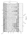
- FIG. 1 is a cross-sectional illustration of a finFET structure before formation of fins.
- FIG. 2 is a cross-sectional illustration of a finFET structure after formation of fins.
- FIG. 3 is a cross-sectional illustration of a finFET structure after formation of fins with the addition of a shallow trench isolation region.
- FIG. 4 is a cross-sectional illustration of a finFET structure after formation and reveal of fins by pulling down of the shallow trench isolation region.
- FIG. 5 is a cross-sectional illustration of a finFET structure after formation of fins and gate stack etching.
- FIG. 6 is a cross-sectional illustration of a finFET structure after spacer deposition.
- FIG. 7 is a cross-sectional illustration of a finFET structure after a first spacer etch pull down.
- FIG. 8 is a cross-sectional illustration of a finFET structure after blocking a first set of fins on the finFET structure.
- FIG. 9 is a cross-sectional illustration of a finFET structure after a second spacer etch pull down.
- FIG. 10 is a cross-sectional illustration of epitaxy growth on a first set of fins and on a second set of fins.
- FIG. 11 is a cross-sectional illustration of the finFET structure of FIG. 10 , taken across line A-A and line B-B in FIG. 10 .
- FinFET integration can be an issue for digital devices having a tight gate pitch (e.g., less than or equal to 90 nanometers (nm) for 14 nm technology node) and analog devices having a large gate pitch (e.g., greater than or equal to 90 nm for 14 nm node) with a thick gate oxide.
- Large gate pitch can leave little to no room for work function metal (WFM) deposition in devices with a tight fin pitch.
- WFM work function metal
- an analog device is often designed with a fin pitch that is at least two times the fin pitch compared to a logic device where the thick gate oxide coating is removed before formation and deposition of the gate (e.g., an active gate for a gate first scheme or a dummy gate for a replacement metal gate (RMG)).
- a fin pitch that is at least two times the fin pitch compared to a logic device where the thick gate oxide coating is removed before formation and deposition of the gate (e.g., an active gate for a gate first scheme or a dummy gate for a replacement metal gate (RMG)).
- RMG replacement metal gate
- fin pitch is large (e.g., greater than or equal to 40 nm)
- FIGS. 1-4 demonstrate how a bulk fin structure is formed.
- FIG. 1 is a cross-sectional view of a finFET structure before formation of fins.
- a substrate 14 is shown with a punch through stopper layer 18 present on the substrate.
- a fin hard mask layer 64 is disposed over the substrate 14 , punch through stopper layer 18 , and channel material 100 .
- Channel material 100 can be the same as or different from the substrate 14 .
- a first fin region 60 and a second fin region 62 are also shown in FIG. 1 .
- a punch through stopper layer 18 (e.g., isolation region) and channel can be grown sequentially from the substrate 14 by multiple epitaxial process with various dopants.
- the Punch through stopper layer 18 can be an in-situ doped epitaxial layer or an ex-situ doped epitaxial layer.
- Non-limiting examples of substrate 14 materials include Si (silicon), strained Si, SiC (silicon carbide), Ge (germanium), SiGe (silicon germanium), SiGeC (silicon-germanium-carbon), Si alloys, Ge alloys, GaAs (gallium arsenide), InAs (indium arsenide), InP (indium phosphide), or a combination comprising at least one of the foregoing.
- the thickness of the substrate 14 generally varies and is not intended to be limited.
- the thickness of the substrate 14 can be about 50 micrometers to about 2000 micrometers.
- FIG. 2 is a cross-sectional view of the finFET structure of FIG. 1 after formation of fins 12 .
- first fins 70 and second fins 72 can be formed by a lithographic patterning and etching process, by a sidewall imaging process, by an e-beam exposure process, or by an e-beam ultraviolet light exposure process.
- the first and second fins 70 , 72 can be formed by etching material from the first fin region 60 and the second fin region 62 using an etching process such as reactive ion etching (ME).
- ME reactive ion etching
- the first and second fins 70 , 72 can have different threshold voltages due to different elemental concentrations (e.g., different silicon germanium concentrations).
- a fin hard mask layer 64 can be disposed over the first and second active regions fins 70 , 72 .
- the first and second fins 70 , 72 can have different elemental concentrations, different heights, and different thicknesses for forming two different transistors as will be explained with respect to FIGS. 8-15 .
- shallow trench isolation (STI) regions 66 have been formed in a first fin pitch area 30 and a second fin pitch area 32 .
- the shallow trench isolation regions 66 are isolation regions that can be formed by etching trenches in the substrate 14 and then filling the trenches with, for example, silicon dioxide. Other oxide materials can be deposited to form the shallow trench isolation regions 66 .
- oxide materials for the shallow trench isolation regions 66 include silicon dioxide, tetraethylorthosilicate (TEOS) oxide, high aspect ratio plasma (HARP) oxide, silicon oxide, high temperature oxide (HTO), high density plasma (HDP) oxide, oxides formed by an atomic layer deposition (ALD) process, or a combination comprising at least one of the foregoing.
- FIG. 4 is a cross-sectional side view after recessing the shallow trench isolation regions 66 .
- the shallow trench isolation regions 66 can be recessed by different amounts (different depths) by removing different amounts of the substrate 14 .
- the shallow trench isolation regions 66 can be recessed such that the shallow trench isolation regions 66 have a thickness of about 4 to about 100 nm, for example, about 6 to about 30 nm.
- the etching process employed to recess the shallow trench isolation regions 66 can be any wet or dry etching process.
- first fins 70 and second fins 72 have been patterned onto a substrate 14 and then a gate stack 16 is formed over fins 70 , 72 .
- a gate stack 16 is formed over fins 70 , 72 .
- fins 70 and 72 are not connected, but rather are located at different areas of the structure.
- dummy gate 22 , first hard mask layer 24 , and second hard mask layer 26 constitute gate stack 16 .
- the first hard mask layer 24 and second hard mask layer 26 can provide protection to the other layers present in the semiconductor device 10 during formation.
- the gate stack 16 can be an active gate for a first scheme or a dummy gate for a replacement metal gate.
- a replacement metal gate can be formed over fins 70 , 72 after epitaxy growth.
- a replacement metal gate (RMG) can be formed over the fin 70 .
- the replacement metal gate can be formed by initially forming a “dummy” gate made of, for example, semiconductor material (e.g. silicon) or dielectric material. The dummy gate material is deposited and etched using known techniques. Then the dummy gate material is removed and replaced with a metal gate material to form the RMG 140 .
- the metal gate material depends on the type of transistor. Non-limiting examples of metal gate materials include titanium, tungsten, tantalum, tantalum nitride, ruthenium, rhenium, tungsten, or a combination comprising at least one of the foregoing.
- the first hard mask layer 24 , and/or second hard mask layer 26 , and/or fin hard mask 64 can comprise any dielectric material (e.g. silicon nitride, silicon dioxide) to assist patterning gates and/or fins.
- dielectric material e.g. silicon nitride, silicon dioxide
- Punch through stopper layer 18 can be etched onto substrate 14 and fins 70 , 72 , e.g., punch through stopper layer 18 can be etched onto protrusion 46 , part of substrate 14 and can extend vertically upward toward punch through stopper layer 18 .
- the punch through stopper layer 18 can be a doped region configured to prevent source to drain shorts acting similarly to buried oxide in a semiconductor on insulator.
- the punch through stopper layer 18 can be formed with a block resist pattern and ion implantation prior to fin formation or can be achieved after fin formation.
- the punch through stopper layer 18 can be formed by forming a spacer to protect the active fins and then the shallow trench isolation recess 66 can then be recessed further and a solid doping layer deposited and this layer then annealed. As previously described herein, a shallow trench isolation recess 66 can be formed within the substrate 14 . As can be seen in FIG. 4 , first fins 70 (e.g., tight fin pitch) and second fins 72 (e.g., loose fin pitch) can have different punch through stopper layer 18 depths and thickness, which can be achieved by blocking one set of fins while pulling down the shallow trench isolation recess 66 on the other set of fins. As illustrated in FIG.
- the fin pitch can vary between a first fin pitch area 30 and a second fin pitch area 32 such that fin pitch 48 , present in first fin pitch area 30 is smaller and fin pitch 38 , present in second fin pitch area 32 .
- a thickness of the punch through stopper layer 18 in second fin pitch area 32 can be smaller with a taller active fin 72 than that in first fin pitch area 30 .
- spacers 28 have been formed around fins 70 , 72 and punch through stopper layer 18 .
- the spacers 28 are created by forming a layer of spacer material 50 over substrate 14 and shallow trench region 66 .
- An anisotropic etch is then performed to pull (e.g., etch) horizontal surfaces of the spacer layer 50 to remove them using a reactive ion etching (ME) plasma process.
- ME reactive ion etching
- Deposition material 52 is covers the gate stack etch structure 16 .
- deposition material 52 is being pulled down over the gate stack etch 16 in a step for a first fin pitch area 30 epitaxy merge.
- spacer layer 50 has been pulled down over a portion of fin 70 from spacer layer 50 toward punch through stopper layer 18 to expose a portion of fin 70 .
- the first fin pitch area 30 is blocked by blocking layer 36 to protect the first fin pitch area 30
- deposition material 52 is being pulled down over gate stack etch 16 in a step to form a second fin pitch area 32 .
- spacer 28 has been pulled down over a portion of fin 70 toward punch through stopper layer 18 to expose a portion of fin 72 using the RIE process.
- the shallow trench isolation region 66 outside of the gate spacer and fin spacer can form recess 42 .
- epitaxy 40 growth is illustrated in first fin pitch area 30 and second fin pitch area 32 around fins 70 and 70 . As demonstrated in FIG. 10 , epitaxy 40 growth can occur on each of the fins 12 in first fin pitch area 30 and second fin pitch area 32 , even with the larger fin pitch 38 in second fin pitch area 32 .
- the epitaxy 40 growth can have a thickness of about 5 nm to about 80 nm. In another aspect, the epitaxy 40 growth has a thickness of about 10 nm to about 40 nm.
- An epitaxial growth process can be used to grow epitaxy 40 (e.g., silicon epitaxy) with various dopants over fins 12 .
- epitaxy 40 e.g., silicon epitaxy
- a non-limiting example of a material (element) for the epitaxial layers 401 includes silicon germanium doped with boron for PMOS and silicon carbon doped with phosphorous for NMOS.
- the epitaxy 40 can be grown using a growth process, for example, chemical vapor deposition (CVD) (liquid phase (LP) or reduced pressure chemical vapor deposition (RPCVD), vapor-phase epitaxy (VPE), molecular-beam epitaxy (MBE), liquid-phase epitaxy (LPE), metal organic chemical vapor deposition (MOCVD), or other processes.
- CVD chemical vapor deposition
- LP liquid phase
- RPCVD reduced pressure chemical vapor deposition
- VPE vapor-phase epitaxy
- MBE molecular-beam epitaxy
- LPE liquid-phase epitaxy
- MOCVD metal organic chemical vapor deposition
- the thickness of the epitaxy 40 in the first fin pitch area 30 and the second fin pitch area 32 can be substantially the same because they will be formed concomitantly through the patterned mask. Because the fin pitch in the first fin pitch area 30 and the second fin pitch area different, epitaxy 40 will protrude from fins 12 by different amounts.
- FIG. 11 is a cross-sectional detailed illustration of fin 70 in first fin pitch area 30 and fin 72 second fin pitch area 32 .
- Spacer 28 can be etched around fin 70 , 72 and punch through stopper layer 18 .
- Epitaxy 40 can be grown around fin channel 44 and dummy gate 22 . As can be seen, spacer 28 located in fin 70 has a higher depth than spacer 28 located in fin 72 .
- a method of forming a semiconductor can include forming a shallow trench isolation recess 66 on a substrate 14 .
- the shallow trench isolation recess 66 can have a depth of 50-200 nanometers (nm), for example, 50 nm, for example, 10 nm.
- a first set of fins 70 comprising fins 12 can be formed on the substrate 14 with a punch through stopper layer 18 disposed between the substrate 14 and the first set of fins 70 in first fin region 60 .
- the first set of fins 70 can have a fin pitch 48 of less than or equal to 35 nm, for example, less than or equal to 34 nm, for example, less than or equal to 27 nm and a height of 5-50 nm.
- a second set of fins 72 comprising fins 12 can be formed on the substrate 14 with a punch through stopper layer 18 disposed between the substrate 14 and the first set of fins 12 in second fin region 62 .
- the second set of fins 72 can have a fin pitch 38 of greater than 40 nm, for example, greater than or equal to 42 nm, for example, greater than or equal to 45 nm and a height of 5-50 nm.
- a spacer 28 can be placed around each fin 12 in the first set of fins 70 and in the second set of fins 72 .
- the spacer 28 can be vertically etched around the first set of fins 70 .
- the first set of fins 70 can be blocked and the spacer 28 can be vertically etched around the second set of fins 72 .
- Epitaxy 40 can be grown on the first set of fins 70 and the second set of fins 72 .
- the epitaxy 40 can be merged on the first set of fins 70 and on the second set of fins 72 to form a semiconductor device 10 with a first set of fins 70 and a second set of fins 72 .
- Each of fins 12 in the first set of fins 70 and the second set of fins 72 can have a height variation of less than or equal to 20 nm, for example, less than or equal to 15 nm, for example, less than or equal to 10 nm, for example, less than or equal to 5 nm.
- a gate stack 16 can be etched over a portion of the first set of fins 60 and the second set of fins 62 .
- the gate stack 16 can comprise a dummy gate 22 , a first hard mask layer (e.g., a gate oxide hard mask) 24 , and a second hard mask layer (e.g., a gate nitride hard mask) 26 disposed between the dummy gate 22 and the first hard mask layer 24 .
- the punch through stopper layer 18 can form a portion of the fins 70 , 72 having a doped layer to assist in preventing source to drain shorts.
- the punch through stopper layer 18 and fins 70 , 72 can be protected with a spacer after reactive ion etching to prevent epitaxy growth.
- the substrate 14 can comprise a semiconductor.
- the substrate 14 can comprise silicon in combination with a Group II to Group V metal, oxides thereof, or a combination comprising at least one of the foregoing.
- the spacer 28 can comprise a low- ⁇ dielectric material.
- the spacer can comprise silicon nitride, silicon boron carbon nitride, silicon oxygen carbon nitride, or a combination comprising at least one of the foregoing.
- a fin field effect transistor can be formed from the semiconductor device 10 .
- a semiconductor device 10 can include a shallow trench isolating recess 66 (e.g., a dielectric layer).
- the shallow trench isolation recess 66 can have a depth of 50-200 nm.
- a substrate 14 can be disposed adjacent to the shallow trench isolating recess 66 .
- the semiconductor device 10 can include a vertically etched first set of fins 70 comprising fins 12 , where a punch through stopper layer 18 can be disposed between the second set of fins 70 and the substrate 14 .
- the semiconductor device 10 can include a vertically etched second set of fins 72 , wherein a punch through stopper layer 18 is disposed between the second set of fins 72 and the substrate 14 .
- a spacer 28 can be disposed around each fin 12 in the first set of fins 70 and in the second set of fins 72 .
- a height of the spacer 28 can be 10-90% smaller as compared to a height of the spacer 28 in the second set of fins 72 after etching the first set of fins 70 and the second set of fins 72 .
- Epitaxy 40 can be grown on the first set of fins 70 and the second set of fins 72 . After growing, the epitaxy 40 on the first set of fins 70 can be merged and the epitaxy 40 on the second set of fins 72 can be merged.
- the STI regions 66 are recessed during fin formation. Etching processes can include wet or dry etching process using HF based chemistry to recess the STI regions 66 .
- compositions comprising, “comprising,” “includes,” “including,” “has,” “having,” “contains” or “containing,” or any other variation thereof, are intended to cover a non-exclusive inclusion.
- a composition, a mixture, process, method, article, or apparatus that comprises a list of elements is not necessarily limited to only those elements but can include other elements not expressly listed or inherent to such composition, mixture, process, method, article, or apparatus.
- invention or “present invention” are non-limiting terms and not intended to refer to any single aspect of the particular invention but encompass all possible aspects as described in the specification and the claims.
- the term “about” modifying the quantity of an ingredient, component, or reactant of the invention employed refers to variation in the numerical quantity that can occur, for example, through typical measuring and liquid handling procedures used for making concentrates or solutions. Furthermore, variation can occur from inadvertent error in measuring procedures, differences in the manufacture, source, or purity of the ingredients employed to make the compositions or carry out the methods, and the like.
- the term “about” means within 10% of the reported numerical value.
- the term “about” means within 5% of the reported numerical value.
- the term “about” means within 10, 9, 8, 7, 6, 5, 4, 3, 2, or 1% of the reported numerical value.
Landscapes
- Insulated Gate Type Field-Effect Transistor (AREA)
Abstract
Description
Claims (20)
Priority Applications (1)
| Application Number | Priority Date | Filing Date | Title |
|---|---|---|---|
| US14/959,407 US9397006B1 (en) | 2015-12-04 | 2015-12-04 | Co-integration of different fin pitches for logic and analog devices |
Applications Claiming Priority (1)
| Application Number | Priority Date | Filing Date | Title |
|---|---|---|---|
| US14/959,407 US9397006B1 (en) | 2015-12-04 | 2015-12-04 | Co-integration of different fin pitches for logic and analog devices |
Publications (1)
| Publication Number | Publication Date |
|---|---|
| US9397006B1 true US9397006B1 (en) | 2016-07-19 |
Family
ID=56381723
Family Applications (1)
| Application Number | Title | Priority Date | Filing Date |
|---|---|---|---|
| US14/959,407 Expired - Fee Related US9397006B1 (en) | 2015-12-04 | 2015-12-04 | Co-integration of different fin pitches for logic and analog devices |
Country Status (1)
| Country | Link |
|---|---|
| US (1) | US9397006B1 (en) |
Cited By (10)
| Publication number | Priority date | Publication date | Assignee | Title |
|---|---|---|---|---|
| US20190067484A1 (en) * | 2017-08-30 | 2019-02-28 | Samsung Electronics Co., Ltd. | Semiconductor device and method for fabricating the same |
| CN109427671A (en) * | 2017-08-30 | 2019-03-05 | 台湾积体电路制造股份有限公司 | Fin structure for semiconductor devices |
| CN110299409A (en) * | 2018-03-23 | 2019-10-01 | 中芯国际集成电路制造(上海)有限公司 | FinFET device and the method for forming epitaxial structure in its source-drain area |
| DE102018113843A1 (en) * | 2018-05-10 | 2019-11-14 | Taiwan Semiconductor Manufacturing Co., Ltd. | Fin and gate dimensions to optimize gate formation |
| CN110880535A (en) * | 2018-09-05 | 2020-03-13 | 三星电子株式会社 | Semiconductor device |
| US10991692B2 (en) * | 2017-04-03 | 2021-04-27 | Samsung Electronics Co., Ltd. | Semiconductor device having a plurality of fins and method of fabricating the same |
| US11127639B2 (en) * | 2019-08-22 | 2021-09-21 | Taiwan Semiconductor Manufacturing Co., Ltd. | Structure and formation method of semiconductor device with fin structures |
| US11177177B2 (en) * | 2018-11-30 | 2021-11-16 | Taiwan Semiconductor Manufacturing Company Limited | Semiconductor device and method of manufacture |
| US11217585B2 (en) * | 2018-09-25 | 2022-01-04 | Taiwan Semiconductor Manufacturing Co., Ltd. | Forming dielectric dummy fins with different heights in different regions of a semiconductor device |
| US12419092B2 (en) | 2017-08-30 | 2025-09-16 | Taiwan Semiconductor Manufacturing Company, Ltd. | Fin structures having varied fin heights for semiconductor device |
Citations (11)
| Publication number | Priority date | Publication date | Assignee | Title |
|---|---|---|---|---|
| US20120032267A1 (en) | 2010-08-06 | 2012-02-09 | International Business Machines Corporation | Device and method for uniform sti recess |
| US8669615B1 (en) * | 2012-08-28 | 2014-03-11 | International Business Machines Corporation | Techniques for metal gate workfunction engineering to enable multiple threshold voltage FINFET devices |
| US8673709B2 (en) | 2009-12-03 | 2014-03-18 | Taiwan Semiconductor Manufacturing Company, Ltd. | FinFETs with multiple fin heights |
| US20140227857A1 (en) | 2013-02-08 | 2014-08-14 | Samsung Electronics Co., Ltd. | Methods of Fabricating Semiconductor Devices Including Fin-Shaped Active Regions |
| US8890261B2 (en) | 2007-06-20 | 2014-11-18 | International Business Machines Corporation | Fin field effect transistor devices with self-aligned source and drain regions |
| US8946038B2 (en) * | 2012-06-12 | 2015-02-03 | Taiwan Semiconductor Manufacturing Company, Ltd. | Diode structures using fin field effect transistor processing and method of forming the same |
| US20150115418A1 (en) | 2013-10-28 | 2015-04-30 | Globalfoundries Inc. | Devices and methods of forming fins at tight fin pitches |
| US20150145070A1 (en) | 2013-11-22 | 2015-05-28 | Qualcomm Incorporated | Merging lithography processes for gate patterning |
| US20150170927A1 (en) | 2013-08-07 | 2015-06-18 | International Business Machines Corporation | Integration of dense and variable pitch fin structures |
| WO2015099691A1 (en) | 2013-12-23 | 2015-07-02 | Intel Corporation | Advanced etching techniques for straight, tall and uniform fins across multiple fin pitch structures |
| US9105510B2 (en) | 2012-12-10 | 2015-08-11 | Globalfoundries Inc. | Double sidewall image transfer process |
-
2015
- 2015-12-04 US US14/959,407 patent/US9397006B1/en not_active Expired - Fee Related
Patent Citations (11)
| Publication number | Priority date | Publication date | Assignee | Title |
|---|---|---|---|---|
| US8890261B2 (en) | 2007-06-20 | 2014-11-18 | International Business Machines Corporation | Fin field effect transistor devices with self-aligned source and drain regions |
| US8673709B2 (en) | 2009-12-03 | 2014-03-18 | Taiwan Semiconductor Manufacturing Company, Ltd. | FinFETs with multiple fin heights |
| US20120032267A1 (en) | 2010-08-06 | 2012-02-09 | International Business Machines Corporation | Device and method for uniform sti recess |
| US8946038B2 (en) * | 2012-06-12 | 2015-02-03 | Taiwan Semiconductor Manufacturing Company, Ltd. | Diode structures using fin field effect transistor processing and method of forming the same |
| US8669615B1 (en) * | 2012-08-28 | 2014-03-11 | International Business Machines Corporation | Techniques for metal gate workfunction engineering to enable multiple threshold voltage FINFET devices |
| US9105510B2 (en) | 2012-12-10 | 2015-08-11 | Globalfoundries Inc. | Double sidewall image transfer process |
| US20140227857A1 (en) | 2013-02-08 | 2014-08-14 | Samsung Electronics Co., Ltd. | Methods of Fabricating Semiconductor Devices Including Fin-Shaped Active Regions |
| US20150170927A1 (en) | 2013-08-07 | 2015-06-18 | International Business Machines Corporation | Integration of dense and variable pitch fin structures |
| US20150115418A1 (en) | 2013-10-28 | 2015-04-30 | Globalfoundries Inc. | Devices and methods of forming fins at tight fin pitches |
| US20150145070A1 (en) | 2013-11-22 | 2015-05-28 | Qualcomm Incorporated | Merging lithography processes for gate patterning |
| WO2015099691A1 (en) | 2013-12-23 | 2015-07-02 | Intel Corporation | Advanced etching techniques for straight, tall and uniform fins across multiple fin pitch structures |
Non-Patent Citations (2)
| Title |
|---|
| Disclosed Anonymously; "Improved FinFET spacer formation"; IPCOM000217324D; May 7, 2012; 6 pages. |
| Disclosed Anonymously; "Variable Fin Pitch Transistors having Wraparound Contact";IPCOM000242337D,Jul. 8, 2015; 4 pages. |
Cited By (25)
| Publication number | Priority date | Publication date | Assignee | Title |
|---|---|---|---|---|
| US10991692B2 (en) * | 2017-04-03 | 2021-04-27 | Samsung Electronics Co., Ltd. | Semiconductor device having a plurality of fins and method of fabricating the same |
| US10784379B2 (en) * | 2017-08-30 | 2020-09-22 | Samsung Electronics Co., Ltd. | Semiconductor device including a shared semiconductor pattern having faceted sidewalls and method for fabricating the same |
| CN109427671A (en) * | 2017-08-30 | 2019-03-05 | 台湾积体电路制造股份有限公司 | Fin structure for semiconductor devices |
| US12419092B2 (en) | 2017-08-30 | 2025-09-16 | Taiwan Semiconductor Manufacturing Company, Ltd. | Fin structures having varied fin heights for semiconductor device |
| US11728434B2 (en) | 2017-08-30 | 2023-08-15 | Samsung Electronics Co., Ltd. | Semiconductor device |
| US20190067484A1 (en) * | 2017-08-30 | 2019-02-28 | Samsung Electronics Co., Ltd. | Semiconductor device and method for fabricating the same |
| US10541319B2 (en) | 2017-08-30 | 2020-01-21 | Taiwan Semiconductor Manufacturing Co., Ltd. | Fin structures having varied fin heights for semiconductor device |
| US11387347B2 (en) | 2017-08-30 | 2022-07-12 | Taiwan Semiconductor Manufacturing Co., Ltd. | Fin structures having varied fin heights for semiconductor device |
| US11133401B2 (en) | 2017-08-30 | 2021-09-28 | Taiwan Semiconductor Manufacturing Co., Ltd. | Fin structures having varied fin heights for semiconductor device |
| CN110299409B (en) * | 2018-03-23 | 2023-02-28 | 中芯国际集成电路制造(上海)有限公司 | FinFET device and method for forming epitaxial structure in source-drain region of FinFET device |
| CN110299409A (en) * | 2018-03-23 | 2019-10-01 | 中芯国际集成电路制造(上海)有限公司 | FinFET device and the method for forming epitaxial structure in its source-drain area |
| DE102018113843A1 (en) * | 2018-05-10 | 2019-11-14 | Taiwan Semiconductor Manufacturing Co., Ltd. | Fin and gate dimensions to optimize gate formation |
| DE102018113843B4 (en) * | 2018-05-10 | 2020-12-31 | Taiwan Semiconductor Manufacturing Co., Ltd. | Fin and gate dimensions to optimize gate formation |
| US10629706B2 (en) * | 2018-05-10 | 2020-04-21 | Taiwan Semiconductor Manufacturing Co., Ltd. | Fin and gate dimensions for optimizing gate formation |
| US20200091320A1 (en) * | 2018-05-10 | 2020-03-19 | Taiwan Semiconductor Manufacturing Co., Ltd. | Fin and Gate Dimensions for Optimizing Gate Formation |
| TWI704691B (en) * | 2018-05-10 | 2020-09-11 | 台灣積體電路製造股份有限公司 | Integrated circuit device and manufacturing method thereof |
| CN110473833A (en) * | 2018-05-10 | 2019-11-19 | 台湾积体电路制造股份有限公司 | Integrated circuit device and method of forming the same |
| US11670703B2 (en) * | 2018-05-10 | 2023-06-06 | Taiwan Semiconductor Manufacturing Co., Ltd. | Fin and gate dimensions for optimizing gate formation |
| CN110880535B (en) * | 2018-09-05 | 2025-08-22 | 三星电子株式会社 | semiconductor devices |
| CN110880535A (en) * | 2018-09-05 | 2020-03-13 | 三星电子株式会社 | Semiconductor device |
| US11616144B2 (en) * | 2018-09-05 | 2023-03-28 | Samsung Electronics Co., Ltd. | Semiconductor device |
| US11217585B2 (en) * | 2018-09-25 | 2022-01-04 | Taiwan Semiconductor Manufacturing Co., Ltd. | Forming dielectric dummy fins with different heights in different regions of a semiconductor device |
| US11776961B2 (en) | 2018-09-25 | 2023-10-03 | Taiwan Semiconductor Manufacturing Co., Ltd. | Semiconductor device and manufacturing method thereof for selectively etching dummy fins |
| US11177177B2 (en) * | 2018-11-30 | 2021-11-16 | Taiwan Semiconductor Manufacturing Company Limited | Semiconductor device and method of manufacture |
| US11127639B2 (en) * | 2019-08-22 | 2021-09-21 | Taiwan Semiconductor Manufacturing Co., Ltd. | Structure and formation method of semiconductor device with fin structures |
Similar Documents
| Publication | Publication Date | Title |
|---|---|---|
| US9397006B1 (en) | Co-integration of different fin pitches for logic and analog devices | |
| US9947804B1 (en) | Methods of forming nanosheet transistor with dielectric isolation of source-drain regions and related structure | |
| US9362355B1 (en) | Nanosheet MOSFET with full-height air-gap spacer | |
| EP3770955B1 (en) | Method for forming a semiconductor device | |
| US9673197B2 (en) | FinFET with constrained source-drain epitaxial region | |
| US8722472B2 (en) | Hybrid CMOS nanowire mesh device and FINFET device | |
| KR101386684B1 (en) | FinFET Design with LDD Extensions | |
| US9761722B1 (en) | Isolation of bulk FET devices with embedded stressors | |
| US9368569B1 (en) | Punch through stopper for semiconductor device | |
| US20140217364A1 (en) | Diode Structure and Method for Wire-Last Nanomesh Technologies | |
| US9793114B2 (en) | Uniform height tall fins with varying silicon germanium concentrations | |
| US9576954B1 (en) | POC process flow for conformal recess fill | |
| US9385123B2 (en) | STI region for small fin pitch in FinFET devices | |
| KR20170026507A (en) | - a method of forming - channel | |
| US10872954B2 (en) | Sidewall image transfer nanosheet | |
| US20170236722A1 (en) | Fin formation for semiconductor device | |
| US20170047256A1 (en) | Forming a contact for a tall fin transistor | |
| US9530890B1 (en) | Parasitic capacitance reduction | |
| US8633077B2 (en) | Transistors with uniaxial stress channels | |
| US9793161B2 (en) | Methods for contact formation for 10 nanometers and beyond with minimal mask counts | |
| US9704994B1 (en) | Different shallow trench isolation fill in fin and non-fin regions of finFET |
Legal Events
| Date | Code | Title | Description |
|---|---|---|---|
| AS | Assignment |
Owner name: INTERNATIONAL BUSINESS MACHINES CORPORATION, NEW Y Free format text: ASSIGNMENT OF ASSIGNORS INTEREST;ASSIGNORS:OK, INJO;PRANATHARTHIHARAN, BALASUBRAMANIAN S.;SEO, SOON-CHEON;AND OTHERS;SIGNING DATES FROM 20151203 TO 20151204;REEL/FRAME:037214/0894 |
|
| STCF | Information on status: patent grant |
Free format text: PATENTED CASE |
|
| MAFP | Maintenance fee payment |
Free format text: PAYMENT OF MAINTENANCE FEE, 4TH YEAR, LARGE ENTITY (ORIGINAL EVENT CODE: M1551); ENTITY STATUS OF PATENT OWNER: LARGE ENTITY Year of fee payment: 4 |
|
| AS | Assignment |
Owner name: ELPIS TECHNOLOGIES INC., CANADA Free format text: ASSIGNMENT OF ASSIGNORS INTEREST;ASSIGNOR:INTERNATIONAL BUSINESS MACHINES CORPORATION;REEL/FRAME:052561/0161 Effective date: 20200306 |
|
| FEPP | Fee payment procedure |
Free format text: MAINTENANCE FEE REMINDER MAILED (ORIGINAL EVENT CODE: REM.); ENTITY STATUS OF PATENT OWNER: LARGE ENTITY |
|
| LAPS | Lapse for failure to pay maintenance fees |
Free format text: PATENT EXPIRED FOR FAILURE TO PAY MAINTENANCE FEES (ORIGINAL EVENT CODE: EXP.); ENTITY STATUS OF PATENT OWNER: LARGE ENTITY |
|
| STCH | Information on status: patent discontinuation |
Free format text: PATENT EXPIRED DUE TO NONPAYMENT OF MAINTENANCE FEES UNDER 37 CFR 1.362 |
|
| FP | Lapsed due to failure to pay maintenance fee |
Effective date: 20240719 |