US9386246B2 - Photoelectric conversion device and image sensor - Google Patents
Photoelectric conversion device and image sensor Download PDFInfo
- Publication number
- US9386246B2 US9386246B2 US14/076,597 US201314076597A US9386246B2 US 9386246 B2 US9386246 B2 US 9386246B2 US 201314076597 A US201314076597 A US 201314076597A US 9386246 B2 US9386246 B2 US 9386246B2
- Authority
- US
- United States
- Prior art keywords
- photoelectric conversion
- output order
- conversion device
- order control
- signal
- Prior art date
- Legal status (The legal status is an assumption and is not a legal conclusion. Google has not performed a legal analysis and makes no representation as to the accuracy of the status listed.)
- Expired - Fee Related, expires
Links
Images


Classifications
-
- H04N5/3694—
-
- H—ELECTRICITY
- H10—SEMICONDUCTOR DEVICES; ELECTRIC SOLID-STATE DEVICES NOT OTHERWISE PROVIDED FOR
- H10F—INORGANIC SEMICONDUCTOR DEVICES SENSITIVE TO INFRARED RADIATION, LIGHT, ELECTROMAGNETIC RADIATION OF SHORTER WAVELENGTH OR CORPUSCULAR RADIATION
- H10F39/00—Integrated devices, or assemblies of multiple devices, comprising at least one element covered by group H10F30/00, e.g. radiation detectors comprising photodiode arrays
- H10F39/10—Integrated devices
- H10F39/12—Image sensors
-
- H—ELECTRICITY
- H04—ELECTRIC COMMUNICATION TECHNIQUE
- H04N—PICTORIAL COMMUNICATION, e.g. TELEVISION
- H04N25/00—Circuitry of solid-state image sensors [SSIS]; Control thereof
- H04N25/70—SSIS architectures; Circuits associated therewith
- H04N25/701—Line sensors
- H04N25/7013—Line sensors using abutted sensors forming a long line
-
- H—ELECTRICITY
- H04—ELECTRIC COMMUNICATION TECHNIQUE
- H04N—PICTORIAL COMMUNICATION, e.g. TELEVISION
- H04N1/00—Scanning, transmission or reproduction of documents or the like, e.g. facsimile transmission; Details thereof
- H04N1/024—Details of scanning heads ; Means for illuminating the original
- H04N1/028—Details of scanning heads ; Means for illuminating the original for picture information pick-up
-
- H—ELECTRICITY
- H04—ELECTRIC COMMUNICATION TECHNIQUE
- H04N—PICTORIAL COMMUNICATION, e.g. TELEVISION
- H04N25/00—Circuitry of solid-state image sensors [SSIS]; Control thereof
- H04N25/70—SSIS architectures; Circuits associated therewith
- H04N25/76—Addressed sensors, e.g. MOS or CMOS sensors
- H04N25/767—Horizontal readout lines, multiplexers or registers
-
- H04N5/3742—
Definitions
- the present invention relates to a photoelectric conversion device and an image sensor, and more particularly, to an image sensor to be applied to an image reading apparatus such as a fax machine and an image scanner.
- FIG. 4 is a block diagram illustrating a conventional image sensor and a conventional photoelectric conversion device that are used in an image reading apparatus.
- a conventional photoelectric conversion device 210 includes a plurality of readout circuit blocks 200 , a signal processing circuit 213 , and a logic circuit 222 .
- the readout circuit blocks 200 and the signal processing circuit 213 are connected to each other by a common signal line 11 .
- the readout circuit blocks 200 and the logic circuit 222 are connected to each other by a control signal line 223 .
- a conventional image sensor includes a plurality of the photoelectric conversion devices 210 , which are connected to each other by signal lines ⁇ SI, ⁇ CLK, ⁇ MODE, ⁇ FS, and SIG and a readout start signal line 224 .
- FIG. 5 is a circuit diagram illustrating the conventional readout circuit block 200 .
- the conventional readout circuit block 200 illustrated in FIG. 5 is configured to read out in 4-bit units.
- the readout circuit block 200 includes four light receiving elements 101 , 102 , 103 , and 104 , source follower amplifiers 120 , signal voltage holding capacitors 131 , reference voltage holding capacitors 132 , signal voltage reading switches 141 , reference voltage reading switches 142 , source follower amplifiers 150 for readout, signal voltage readout switches 161 , reference voltage readout switches 162 , readout selection switches 170 , the common signal line 211 , the signal processing circuit 213 , four flip-flops 180 forming a shift register, three switches 112 , 113 , and 114 provided between the light receiving elements, and two reset switches 111 and 115 serving as reset means.
- the readout circuit block 200 is configured so that the number of the light receiving elements is equal to the number of the flip-flops, and optical signals generated by all photoelectric conversion means through one scanning are output to the common signal line. Further, the signals to be input to the readout circuit block 200 (such as ⁇ C 1 , ⁇ C 2 , and ⁇ C 3 ) are generated in the logic circuit 222 .
- the readout circuit block 200 controls the clock signals ⁇ C 1 , ⁇ C 2 , and ⁇ C 3 to be supplied to the shift register to perform resolution switching (for example, see Japanese Patent Application Laid-open No. 2006-25352).
- the present invention has been made to solve such a conventional problem, and can provide a small-area photoelectric conversion device by reducing the number of flip-flops forming a shift register without impairing a resolution switching function.
- a photoelectric conversion device includes: a photoelectric conversion block including: a plurality of photoelectric conversion elements for outputting electrical signals in accordance with incident light; and a plurality of capacitors for storing the electrical signals of the plurality of photoelectric conversion elements; a light reception signal control switch block including a plurality of light reception signal control switches for reading out the electrical signals stored in the plurality of capacitors to a common readout line; an output order control switch block including n units including j output order control switches for controlling on and off of the plurality of light reception signal control switches, where n and j are each a natural number of 2 or more; an output order control circuit for outputting an output order control signal for sequentially turning on the j output order control switches; and a shift register for outputting, to the n units, a shift register control signal for sequentially turning on the j output order control switches.
- an image sensor includes a plurality of the photoelectric conversion devices, which are connected to each other.
- the photoelectric conversion device of the present invention there is an effect that a small-area photoelectric conversion device can be provided by reducing the number of flip-flops forming the shift register without impairing the resolution switching function.
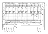
- FIG. 1 is a block diagram illustrating an image sensor according to an embodiment of the present invention
- FIG. 2 is a circuit diagram illustrating a configuration of a photoelectric conversion device according to the embodiment of the present invention
- FIG. 3 is a block diagram illustrating a configuration of a holding circuit
- FIG. 4 is a block diagram illustrating a conventional image sensor and a conventional photoelectric conversion device.
- FIG. 5 is a circuit diagram illustrating a readout circuit block of a conventional image reading apparatus.
- FIG. 1 is a block diagram illustrating an image sensor according to an embodiment of the present invention
- the image sensor of this embodiment includes a plurality of (for example, m) photoelectric conversion devices 1 that are arranged and mounted in one row.
- Each of the photoelectric conversion devices 1 includes an SI terminal for receiving a readout start signal ⁇ SI, a CS terminal for receiving a chip select signal ⁇ SI 2 , a CLK terminal for inputting a clock ⁇ CLK, a MODE terminal for receiving a resolution switching signal ⁇ MODE, an FS terminal for receiving a start pulse ⁇ FS, an SIG terminal for outputting a light reception signal SIG, and an SO terminal for outputting a readout signal.
- the readout start signal ⁇ SI is input to the SI terminal of a first photoelectric conversion device 1 - a .
- the SI terminals of second to m-th photoelectric conversion devices 1 - b to 1 - m are each connected to the SO terminal of the preceding stage.
- the CS terminal of the first photoelectric conversion device 1 - a is connected to the SO terminal of the m-th photoelectric conversion device 1 - m .
- the clock ⁇ CLK is input to the CLK terminals in common.
- the resolution switching signal ⁇ MODE is input to the MODE terminals in common.
- the start pulse ⁇ FS is input to the FS terminals in common.
- the SIG terminals each output the light reception signal SIG.
- FIG. 2 is a circuit diagram illustrating the configuration of the photoelectric conversion device 1 according to this embodiment.
- the photoelectric conversion device 1 includes a photoelectric conversion block 2 including a plurality of (for example, t) photoelectric conversion elements and capacitors, a light reception signal control switch block 3 , an output order control switch block 4 , an output order control circuit 5 , a shift register 8 formed of flip-flops 7 - 1 to 7 - n , a signal processing circuit 11 , a logic circuit 12 , a reference voltage circuit 20 , an output order control signal line 6 , a shift register control signal line 9 , a common signal line 10 , output order control lines 21 - 1 to 21 - j , an SI terminal 13 , a CS terminal 14 , a CLK terminal 15 , a MODE terminal 16 , an FS terminal 17 , an SIG terminal 18 , and an SO terminal 19 .
- the respective circuit elements of the photoelectric conversion device 1 form n photoelectric conversion units U- 1 to U-n each including j photoelectric conversion elements and respective circuit elements corresponding thereto as one group.
- the photoelectric conversion block 2 is connected to the common signal line 10 via the light reception signal control switch block 3 .
- the common signal line 10 is connected to the SIG terminal 18 via the signal processing circuit 11 .
- the SI terminal 13 , the CS terminal 14 , the CLK terminal 15 , the MODE terminal 16 , and the FS terminal 17 are connected to the logic circuit 12 .
- the logic circuit 12 is connected to the output order control circuit 5 by the output order control signal line 6 , and is connected to the shift register 8 by the shift register control signal line 9 .
- the output order control switch block 4 is connected to the control lines of the output order control circuit 5 , the shift register 8 , and the reference voltage circuit 20 to control the light reception signal control switch block 3 by the respective control lines.
- the common signal line 10 may be connected to a constant current source.
- the photoelectric conversion element converts incident light into an electrical signal (light reception signal SIG), and stores the light reception signal SIG in the capacitor.
- the light reception signal SIG stored in the capacitor is sequentially read out to the common signal line 10 via the light reception signal control switch block 3 .
- the light reception signal SIG is output to the SIG terminal 18 via the signal processing circuit 11 .
- the output order control switch block 4 selects the photoelectric conversion element from which the signal is read out in the photoelectric conversion unit U.
- the output order control circuit 5 outputs an output order control signal for controlling the output order control switch block 4 via the output order control lines 21 - 1 to 21 - j .
- the reference voltage circuit 20 supplies a reference voltage to the output order control switch block 4 .
- the logic circuit 12 generates, based on respective signals input to the SI terminal 13 , the CS terminal 14 , the CLK terminal 15 , the MODE terminal 16 , and the FS terminal 17 , a shift register control signal for controlling the shift register 8 and the output order control signal for controlling the output order control circuit 5 .
- the shift register 8 sequentially transfers the shift register control signal from the flip-flop 7 - 1 in the initial stage to the flip-flop 7 - n in the final stage, and further outputs the shift register control signal to the output order control switch block 4 .
- the k-th flip-flop 7 - k has an output connected to the SO terminal 19 .
- the logic circuit 12 includes therein a holding circuit 50 for holding a signal input to the CS terminal 14 at the time of start of readout.
- FIG. 3 is a block diagram illustrating the configuration of the holding circuit 50 .
- the holding circuit 50 of FIG. 3 includes a flip-flop 51 , a single-pulse generating circuit 52 , and a reset control circuit 53 .
- the flip-flop 51 has a terminal D connected to the CS terminal 14 , a terminal CLK connected to the single-pulse generating circuit 52 , a terminal RX connected to the reset control circuit 53 , and a terminal Q connected to the output order control circuit 5 via the output order control signal line 6 .
- the single-pulse generating circuit 52 generates a pulse when the start pulse ⁇ FS is input. Therefore, the flip-flop 51 holds a signal input to the terminal D, that is, the CS terminal 14 at this time, and outputs the signal to the terminal Q.
- the logic circuit 12 determines, based on the data of the terminal Q of the flip-flop 51 , whether the photoelectric conversion device is the first photoelectric conversion device 1 or the photoelectric conversion device 1 in the second or subsequent stage.
- the CS terminal 14 of the photoelectric conversion device 1 - a is connected to the SO terminal 19 (for example, Lo level) of the photoelectric conversion device 1 - m
- the chip select signal ⁇ SI 2 (for example, Hi level) is input to the CS terminals 14 of the photoelectric conversion devices 1 - b to 1 - m .
- the data of the terminal Q of the flip-flop 51 of the first photoelectric conversion device 1 - a is Lo level
- the data of the terminals Q of the flip-flops 51 of the photoelectric conversion devices 1 - b to 1 - m are Hi level.
- whether each of the photoelectric conversion devices 1 - a to 1 - m is the first photoelectric conversion device or not is determined.
- the photoelectric conversion device 1 is configured so that a plurality of resolutions can be obtained depending on the data of the resolution switching signal ⁇ MODE.
- the output order control circuit 5 controls on and off of output order control switches of the output order control switch block 4 via the output order control lines 21 - 1 to 21 - j to switch the resolution. For example, when two adjacent output order control switches of the output order control switch block 4 are simultaneously turned on or off, the resolution becomes 1/2.
- the output order control switches of the output order control switch block 4 are provided in the number corresponding to the number of the photoelectric conversion elements, and the same number of flip-flops 7 are necessary in the shift register 8 for outputting signals for controlling those output order control switches.
- the photoelectric conversion device 1 of this embodiment configured to select the output order control switches by the output order control circuit 5 and the shift register 8 , when the number of the output order control lines 21 is j, the number of the flip-flops 7 may be 1/j.
- the image sensor In response to input of the readout start signal ⁇ SI to the SI terminal 13 of the first photoelectric conversion device 1 - a after the photoelectric conversion elements of the photoelectric conversion block 2 store an optical signal for a predetermined time period, the image sensor starts the readout operation.
- the logic circuit 12 In response to the input of the readout start signal ⁇ SI, the logic circuit 12 generates the output order control signal and the shift register control signal. In response to the input of the output order control signal, the output order control circuit 5 controls the output order control switches connected to the output order control line 21 - 1 so as to establish a conduction state between the output signal of the shift register 8 and a switch control section for the switch of the light reception signal control switch block 3 . Further, the output order control circuit 5 controls the output order control switches connected to the output order control lines 21 - 2 to 21 - j so that the switch control sections for the switches of the light reception signal control switch block 3 become the reference voltage.
- the shift register 8 In response to the input of the shift register control signal, the shift register 8 outputs a signal for the flip-flop 7 - 1 corresponding to the photoelectric conversion unit U- 1 to turn on the switches of the light reception signal control switch block 3 , and outputs signals for the other flip-flops 7 - 2 to 7 - n to turn off the switches of the light reception signal control switch block 3 . Therefore, the first photoelectric conversion element of the photoelectric conversion unit U- 1 is connected to the common signal line 10 to output the light reception signal SIG to the SIG terminal 18 via the signal processing circuit 11 .
- the output order control circuit 5 sequentially outputs the control signals to the output order control lines 21 - 2 to 21 - j so as to turn on the output order control switches.
- the light reception signals SIG of the second to j-th photoelectric conversion elements of the photoelectric conversion unit U- 1 are sequentially output.
- the shift register 8 outputs signals for the flip-flop 7 - 2 to the flip-flop 7 - n to turn on the switches of the light reception signal control switch block 3 . Then, after the light reception signal SIG of the final photoelectric conversion element of the final photoelectric conversion unit U-n is output, the readout of the signals of the first photoelectric conversion device 1 is completed.
- the signal of the flip-flop 7 - k is output to the SO terminal 19 to be input to the SI terminal 13 of the second photoelectric conversion device 1 . That is, based on the signal of the flip-flop 7 - k , preparation of the readout operation of the next photoelectric conversion device 1 is started. At this time, k may be appropriately determined in accordance with a delay time period for starting the readout operation after the photoelectric conversion device 1 inputs the signal to the SI terminal 13 . By configuring the photoelectric conversion device 1 as described above, the readout operation at the time of switch of the photoelectric conversion device 1 can be seamlessly executed.
- the readout operation is sequentially performed from the first photoelectric conversion device 1 - a to the final photoelectric conversion device 1 - m.
- the CS terminal 14 of the photoelectric conversion device 1 - a is connected to the SO terminal 19 of the photoelectric conversion device 1 - m to input the signal of the flip-flop 7 - k of the photoelectric conversion device 1 - m.
- the photoelectric conversion device 1 - a is designated as the first photoelectric conversion device, and hence the logic circuit 12 is set so that the signal input to the CS terminal 14 acts similarly to the readout start signal ⁇ SI. That is, the photoelectric conversion device 1 - a receives the signal of the SO terminal 19 of the photoelectric conversion device 1 - m to start the preparation of the readout operation.
- the number of the flip-flops 7 forming the shift register 8 can be reduced to 1/j, and hence the chip area can be reduced. Further, as compared to the conventional image sensor, a switch is unnecessary for the readout path of the light reception signal SIG, and hence there is achieved such an effect that no noise increase is caused due to the on-resistance of the switch.
- the photoelectric conversion block 2 may include two capacitors with respect to a photoelectric conversion element so as to store an optical signal and a reference charge and output a difference therebetween. Even with this configuration, similar effects can be obtained.
Landscapes
- Engineering & Computer Science (AREA)
- Multimedia (AREA)
- Signal Processing (AREA)
- Facsimile Heads (AREA)
- Power Engineering (AREA)
- Physics & Mathematics (AREA)
- General Physics & Mathematics (AREA)
- Spectroscopy & Molecular Physics (AREA)
- Solid State Image Pick-Up Elements (AREA)
- Transforming Light Signals Into Electric Signals (AREA)
Abstract
Description
Claims (5)
Applications Claiming Priority (2)
| Application Number | Priority Date | Filing Date | Title |
|---|---|---|---|
| JP2012-251588 | 2012-11-15 | ||
| JP2012251588A JP2014099806A (en) | 2012-11-15 | 2012-11-15 | Photoelectric conversion device and image sensor |
Publications (2)
| Publication Number | Publication Date |
|---|---|
| US20140131552A1 US20140131552A1 (en) | 2014-05-15 |
| US9386246B2 true US9386246B2 (en) | 2016-07-05 |
Family
ID=50680781
Family Applications (1)
| Application Number | Title | Priority Date | Filing Date |
|---|---|---|---|
| US14/076,597 Expired - Fee Related US9386246B2 (en) | 2012-11-15 | 2013-11-11 | Photoelectric conversion device and image sensor |
Country Status (5)
| Country | Link |
|---|---|
| US (1) | US9386246B2 (en) |
| JP (1) | JP2014099806A (en) |
| KR (1) | KR20140063412A (en) |
| CN (1) | CN103826073A (en) |
| TW (1) | TWI603621B (en) |
Families Citing this family (1)
| Publication number | Priority date | Publication date | Assignee | Title |
|---|---|---|---|---|
| JP7467380B2 (en) * | 2021-03-18 | 2024-04-15 | 株式会社東芝 | Solid-state imaging device |
Citations (3)
| Publication number | Priority date | Publication date | Assignee | Title |
|---|---|---|---|---|
| US20040032628A1 (en) * | 2002-07-15 | 2004-02-19 | Brother Kogyo Kabushiki Kaisha | Image sensor for reading image and image reading apparatus including the image sensor |
| JP2006025352A (en) | 2004-07-09 | 2006-01-26 | Seiko Instruments Inc | Photoelectric transducer, signal reader circuit and image sensor |
| US20070145244A1 (en) * | 2005-12-19 | 2007-06-28 | Masahiro Yokomichi | Image sensor |
Family Cites Families (9)
| Publication number | Priority date | Publication date | Assignee | Title |
|---|---|---|---|---|
| JPH0817436B2 (en) * | 1990-08-30 | 1996-02-21 | 富士ゼロックス株式会社 | Signal correction circuit and image sensor |
| US5251270A (en) * | 1990-08-30 | 1993-10-05 | Fuji Xerox Co., Ltd. | Matrix calculating circuit |
| JP3006216B2 (en) * | 1991-09-05 | 2000-02-07 | 富士ゼロックス株式会社 | Two-dimensional contact type image sensor and driving method thereof |
| JPH0779315A (en) * | 1993-06-28 | 1995-03-20 | Fuji Xerox Co Ltd | Picture reader |
| JP3483455B2 (en) * | 1998-02-19 | 2004-01-06 | キヤノン株式会社 | Image sensor and image reading device |
| JP3466953B2 (en) * | 1999-04-12 | 2003-11-17 | キヤノン株式会社 | Image sensor |
| JP2002101261A (en) * | 2000-09-26 | 2002-04-05 | Rohm Co Ltd | Image read device |
| WO2011093225A1 (en) * | 2010-01-26 | 2011-08-04 | 国立大学法人静岡大学 | Solid-state imaging device and method of reading signals from the pixel array of solid-state imaging device |
| TWI567735B (en) * | 2011-03-31 | 2017-01-21 | 半導體能源研究所股份有限公司 | Memory circuit, memory unit, and signal processing circuit |
-
2012
- 2012-11-15 JP JP2012251588A patent/JP2014099806A/en active Pending
-
2013
- 2013-09-24 TW TW102134298A patent/TWI603621B/en not_active IP Right Cessation
- 2013-10-15 CN CN201310481248.XA patent/CN103826073A/en active Pending
- 2013-11-04 KR KR1020130132940A patent/KR20140063412A/en not_active Withdrawn
- 2013-11-11 US US14/076,597 patent/US9386246B2/en not_active Expired - Fee Related
Patent Citations (4)
| Publication number | Priority date | Publication date | Assignee | Title |
|---|---|---|---|---|
| US20040032628A1 (en) * | 2002-07-15 | 2004-02-19 | Brother Kogyo Kabushiki Kaisha | Image sensor for reading image and image reading apparatus including the image sensor |
| JP2006025352A (en) | 2004-07-09 | 2006-01-26 | Seiko Instruments Inc | Photoelectric transducer, signal reader circuit and image sensor |
| US8058599B2 (en) | 2004-07-09 | 2011-11-15 | Seiko Instruments Inc. | Photoelectric converter, image sensor, and signal reading circuit |
| US20070145244A1 (en) * | 2005-12-19 | 2007-06-28 | Masahiro Yokomichi | Image sensor |
Also Published As
| Publication number | Publication date |
|---|---|
| JP2014099806A (en) | 2014-05-29 |
| TWI603621B (en) | 2017-10-21 |
| KR20140063412A (en) | 2014-05-27 |
| US20140131552A1 (en) | 2014-05-15 |
| CN103826073A (en) | 2014-05-28 |
| TW201427417A (en) | 2014-07-01 |
Similar Documents
| Publication | Publication Date | Title |
|---|---|---|
| US9398238B2 (en) | Semiconductor device, physical information acquiring apparatus, and signal reading-out method | |
| US7633540B2 (en) | Image pickup apparatus and image reading apparatus using image pickup apparatus | |
| CN101931411B (en) | A/D conversion apparatus, solid-state image capturing apparatus and electronic information device | |
| US20060262205A1 (en) | Column analog-to-digital conversion apparatus and method supporting a high frame rate in a sub-sampling mode | |
| US9848154B2 (en) | Comparator with correlated double sampling scheme and operating method thereof | |
| US10097781B2 (en) | Analog-to-digital converter and operating method thereof | |
| JP2014146849A (en) | Imaging device, method for driving the same, and imaging system | |
| CN112449134B (en) | Image sensor, address decoder, and image processing system | |
| US7746521B2 (en) | Analog-to-digital conversion in CMOS image sensor | |
| CN112087584B (en) | Analog-to-digital converter and image sensor including the same | |
| KR102546191B1 (en) | Analog-digital converting apparatus and operating method, and cmos image sensor thereof using that | |
| US9386246B2 (en) | Photoelectric conversion device and image sensor | |
| US9007252B1 (en) | Analog to digital conversion method and related analog to digital converter | |
| KR0178521B1 (en) | Linear Image Sensor | |
| US9148603B2 (en) | Offset injection in an analog-to-digital converter | |
| US7630104B2 (en) | Image sensor | |
| US7250592B2 (en) | Image sensor with improved sensitivity and method for driving the same | |
| US20070216792A1 (en) | Solid-state imaging device and method of operating solid-state imaging device | |
| US8632010B2 (en) | Photoelectric conversion apparatus and driving method thereof | |
| KR102339605B1 (en) | Read out circuit and image sensor including the same | |
| JP5144177B2 (en) | Information processing device | |
| JP2006109377A (en) | Image sensor and image processing apparatus | |
| KR20060020244A (en) | CMOS image sensor |
Legal Events
| Date | Code | Title | Description |
|---|---|---|---|
| AS | Assignment |
Owner name: SEIKO INSTRUMENTS INC., JAPAN Free format text: ASSIGNMENT OF ASSIGNORS INTEREST;ASSIGNORS:TOMIOKA, TSUTOMU;MURAOKA, DAISUKE;REEL/FRAME:031577/0678 Effective date: 20130911 |
|
| AS | Assignment |
Owner name: SII SEMICONDUCTOR CORPORATION ., JAPAN Free format text: ASSIGNMENT OF ASSIGNORS INTEREST;ASSIGNOR:SEIKO INSTRUMENTS INC;REEL/FRAME:037783/0166 Effective date: 20160209 |
|
| AS | Assignment |
Owner name: SII SEMICONDUCTOR CORPORATION, JAPAN Free format text: CORRECTIVE ASSIGNMENT TO CORRECT THE EXECUTION DATE PREVIOUSLY RECORDED AT REEL: 037783 FRAME: 0166. ASSIGNOR(S) HEREBY CONFIRMS THE ASSIGNMENT;ASSIGNOR:SEIKO INSTRUMENTS INC;REEL/FRAME:037903/0928 Effective date: 20160201 |
|
| ZAAA | Notice of allowance and fees due |
Free format text: ORIGINAL CODE: NOA |
|
| ZAAB | Notice of allowance mailed |
Free format text: ORIGINAL CODE: MN/=. |
|
| STCF | Information on status: patent grant |
Free format text: PATENTED CASE |
|
| AS | Assignment |
Owner name: ABLIC INC., JAPAN Free format text: CHANGE OF NAME;ASSIGNOR:SII SEMICONDUCTOR CORPORATION;REEL/FRAME:045567/0927 Effective date: 20180105 |
|
| MAFP | Maintenance fee payment |
Free format text: PAYMENT OF MAINTENANCE FEE, 4TH YEAR, LARGE ENTITY (ORIGINAL EVENT CODE: M1551); ENTITY STATUS OF PATENT OWNER: LARGE ENTITY Year of fee payment: 4 |
|
| AS | Assignment |
Owner name: ABLIC INC., JAPAN Free format text: CHANGE OF ADDRESS;ASSIGNOR:ABLIC INC.;REEL/FRAME:064021/0575 Effective date: 20230424 |
|
| FEPP | Fee payment procedure |
Free format text: MAINTENANCE FEE REMINDER MAILED (ORIGINAL EVENT CODE: REM.); ENTITY STATUS OF PATENT OWNER: LARGE ENTITY |
|
| LAPS | Lapse for failure to pay maintenance fees |
Free format text: PATENT EXPIRED FOR FAILURE TO PAY MAINTENANCE FEES (ORIGINAL EVENT CODE: EXP.); ENTITY STATUS OF PATENT OWNER: LARGE ENTITY |
|
| STCH | Information on status: patent discontinuation |
Free format text: PATENT EXPIRED DUE TO NONPAYMENT OF MAINTENANCE FEES UNDER 37 CFR 1.362 |
|
| FP | Lapsed due to failure to pay maintenance fee |
Effective date: 20240705 |