US9378920B2 - Electron emission device and electron emission display - Google Patents
Electron emission device and electron emission display Download PDFInfo
- Publication number
- US9378920B2 US9378920B2 US14/600,000 US201514600000A US9378920B2 US 9378920 B2 US9378920 B2 US 9378920B2 US 201514600000 A US201514600000 A US 201514600000A US 9378920 B2 US9378920 B2 US 9378920B2
- Authority
- US
- United States
- Prior art keywords
- electron emission
- layer
- carbon nanotube
- electron
- electrode
- Prior art date
- Legal status (The legal status is an assumption and is not a legal conclusion. Google has not performed a legal analysis and makes no representation as to the accuracy of the status listed.)
- Active
Links
- 239000004065 semiconductor Substances 0.000 claims abstract description 64
- OKTJSMMVPCPJKN-UHFFFAOYSA-N Carbon Chemical compound [C] OKTJSMMVPCPJKN-UHFFFAOYSA-N 0.000 claims description 187
- 239000002041 carbon nanotube Substances 0.000 claims description 151
- 229910021393 carbon nanotube Inorganic materials 0.000 claims description 151
- 239000002238 carbon nanotube film Substances 0.000 claims description 43
- 239000000463 material Substances 0.000 claims description 31
- 229910021389 graphene Inorganic materials 0.000 claims description 29
- 239000000758 substrate Substances 0.000 claims description 26
- BASFCYQUMIYNBI-UHFFFAOYSA-N platinum Chemical compound [Pt] BASFCYQUMIYNBI-UHFFFAOYSA-N 0.000 claims description 10
- OAICVXFJPJFONN-UHFFFAOYSA-N Phosphorus Chemical compound [P] OAICVXFJPJFONN-UHFFFAOYSA-N 0.000 claims description 9
- KDLHZDBZIXYQEI-UHFFFAOYSA-N Palladium Chemical compound [Pd] KDLHZDBZIXYQEI-UHFFFAOYSA-N 0.000 claims description 8
- 229910052697 platinum Inorganic materials 0.000 claims description 5
- PCHJSUWPFVWCPO-UHFFFAOYSA-N gold Chemical group [Au] PCHJSUWPFVWCPO-UHFFFAOYSA-N 0.000 claims description 4
- 229910052737 gold Inorganic materials 0.000 claims description 4
- 239000010931 gold Substances 0.000 claims description 4
- 229910052763 palladium Inorganic materials 0.000 claims description 4
- 229910052706 scandium Inorganic materials 0.000 claims description 4
- SIXSYDAISGFNSX-UHFFFAOYSA-N scandium atom Chemical compound [Sc] SIXSYDAISGFNSX-UHFFFAOYSA-N 0.000 claims description 4
- VBJZVLUMGGDVMO-UHFFFAOYSA-N hafnium atom Chemical compound [Hf] VBJZVLUMGGDVMO-UHFFFAOYSA-N 0.000 claims description 2
- 238000005411 Van der Waals force Methods 0.000 claims 1
- 229910052735 hafnium Inorganic materials 0.000 claims 1
- 239000010410 layer Substances 0.000 description 204
- 238000000034 method Methods 0.000 description 35
- VYPSYNLAJGMNEJ-UHFFFAOYSA-N silicon dioxide Inorganic materials O=[Si]=O VYPSYNLAJGMNEJ-UHFFFAOYSA-N 0.000 description 10
- 238000004519 manufacturing process Methods 0.000 description 8
- 229910052751 metal Inorganic materials 0.000 description 8
- 239000002184 metal Substances 0.000 description 8
- 239000003960 organic solvent Substances 0.000 description 8
- 238000007740 vapor deposition Methods 0.000 description 8
- 238000000231 atomic layer deposition Methods 0.000 description 6
- 239000011521 glass Substances 0.000 description 5
- 239000002356 single layer Substances 0.000 description 5
- 238000005229 chemical vapour deposition Methods 0.000 description 4
- 238000001755 magnetron sputter deposition Methods 0.000 description 4
- 235000012239 silicon dioxide Nutrition 0.000 description 4
- 239000000377 silicon dioxide Substances 0.000 description 4
- ZOKXTWBITQBERF-UHFFFAOYSA-N Molybdenum Chemical compound [Mo] ZOKXTWBITQBERF-UHFFFAOYSA-N 0.000 description 3
- 239000005083 Zinc sulfide Substances 0.000 description 3
- 238000000151 deposition Methods 0.000 description 3
- 230000000694 effects Effects 0.000 description 3
- 229910001092 metal group alloy Inorganic materials 0.000 description 3
- BPUBBGLMJRNUCC-UHFFFAOYSA-N oxygen(2-);tantalum(5+) Chemical compound [O-2].[O-2].[O-2].[O-2].[O-2].[Ta+5].[Ta+5] BPUBBGLMJRNUCC-UHFFFAOYSA-N 0.000 description 3
- 238000002360 preparation method Methods 0.000 description 3
- 238000001878 scanning electron micrograph Methods 0.000 description 3
- 229910001936 tantalum oxide Inorganic materials 0.000 description 3
- 229910052984 zinc sulfide Inorganic materials 0.000 description 3
- DRDVZXDWVBGGMH-UHFFFAOYSA-N zinc;sulfide Chemical compound [S-2].[Zn+2] DRDVZXDWVBGGMH-UHFFFAOYSA-N 0.000 description 3
- 229910052581 Si3N4 Inorganic materials 0.000 description 2
- XLOMVQKBTHCTTD-UHFFFAOYSA-N Zinc monoxide Chemical compound [Zn]=O XLOMVQKBTHCTTD-UHFFFAOYSA-N 0.000 description 2
- UMIVXZPTRXBADB-UHFFFAOYSA-N benzocyclobutene Chemical compound C1=CC=C2CCC2=C1 UMIVXZPTRXBADB-UHFFFAOYSA-N 0.000 description 2
- 239000000919 ceramic Substances 0.000 description 2
- 229910003460 diamond Inorganic materials 0.000 description 2
- 239000010432 diamond Substances 0.000 description 2
- 238000009826 distribution Methods 0.000 description 2
- 238000010329 laser etching Methods 0.000 description 2
- 229910052750 molybdenum Inorganic materials 0.000 description 2
- 239000011733 molybdenum Substances 0.000 description 2
- 238000000059 patterning Methods 0.000 description 2
- 238000005240 physical vapour deposition Methods 0.000 description 2
- 238000001020 plasma etching Methods 0.000 description 2
- 229920003229 poly(methyl methacrylate) Polymers 0.000 description 2
- 239000004926 polymethyl methacrylate Substances 0.000 description 2
- 239000000843 powder Substances 0.000 description 2
- HBMJWWWQQXIZIP-UHFFFAOYSA-N silicon carbide Chemical compound [Si+]#[C-] HBMJWWWQQXIZIP-UHFFFAOYSA-N 0.000 description 2
- HQVNEWCFYHHQES-UHFFFAOYSA-N silicon nitride Chemical compound N12[Si]34N5[Si]62N3[Si]51N64 HQVNEWCFYHHQES-UHFFFAOYSA-N 0.000 description 2
- 238000004544 sputter deposition Methods 0.000 description 2
- 238000001039 wet etching Methods 0.000 description 2
- PFNQVRZLDWYSCW-UHFFFAOYSA-N (fluoren-9-ylideneamino) n-naphthalen-1-ylcarbamate Chemical compound C12=CC=CC=C2C2=CC=CC=C2C1=NOC(=O)NC1=CC=CC2=CC=CC=C12 PFNQVRZLDWYSCW-UHFFFAOYSA-N 0.000 description 1
- WUPHOULIZUERAE-UHFFFAOYSA-N 3-(oxolan-2-yl)propanoic acid Chemical compound OC(=O)CCC1CCCO1 WUPHOULIZUERAE-UHFFFAOYSA-N 0.000 description 1
- 239000004925 Acrylic resin Substances 0.000 description 1
- 229920000178 Acrylic resin Polymers 0.000 description 1
- 229910052582 BN Inorganic materials 0.000 description 1
- PZNSFCLAULLKQX-UHFFFAOYSA-N Boron nitride Chemical compound N#B PZNSFCLAULLKQX-UHFFFAOYSA-N 0.000 description 1
- XMWRBQBLMFGWIX-UHFFFAOYSA-N C60 fullerene Chemical class C12=C3C(C4=C56)=C7C8=C5C5=C9C%10=C6C6=C4C1=C1C4=C6C6=C%10C%10=C9C9=C%11C5=C8C5=C8C7=C3C3=C7C2=C1C1=C2C4=C6C4=C%10C6=C9C9=C%11C5=C5C8=C3C3=C7C1=C1C2=C4C6=C2C9=C5C3=C12 XMWRBQBLMFGWIX-UHFFFAOYSA-N 0.000 description 1
- 229910003481 amorphous carbon Inorganic materials 0.000 description 1
- 230000004888 barrier function Effects 0.000 description 1
- 229910052980 cadmium sulfide Inorganic materials 0.000 description 1
- UHYPYGJEEGLRJD-UHFFFAOYSA-N cadmium(2+);selenium(2-) Chemical compound [Se-2].[Cd+2] UHYPYGJEEGLRJD-UHFFFAOYSA-N 0.000 description 1
- 229910052799 carbon Inorganic materials 0.000 description 1
- 150000001721 carbon Chemical group 0.000 description 1
- 125000004432 carbon atom Chemical group C* 0.000 description 1
- 239000002131 composite material Substances 0.000 description 1
- 150000001875 compounds Chemical class 0.000 description 1
- 239000004020 conductor Substances 0.000 description 1
- 238000005520 cutting process Methods 0.000 description 1
- 230000007547 defect Effects 0.000 description 1
- 239000002079 double walled nanotube Substances 0.000 description 1
- 230000005684 electric field Effects 0.000 description 1
- 238000004924 electrostatic deposition Methods 0.000 description 1
- 238000005516 engineering process Methods 0.000 description 1
- 229910003472 fullerene Inorganic materials 0.000 description 1
- 125000000524 functional group Chemical group 0.000 description 1
- 229910002804 graphite Inorganic materials 0.000 description 1
- 239000010439 graphite Substances 0.000 description 1
- 239000012535 impurity Substances 0.000 description 1
- AMGQUBHHOARCQH-UHFFFAOYSA-N indium;oxotin Chemical compound [In].[Sn]=O AMGQUBHHOARCQH-UHFFFAOYSA-N 0.000 description 1
- 239000011810 insulating material Substances 0.000 description 1
- 238000009830 intercalation Methods 0.000 description 1
- 230000002687 intercalation Effects 0.000 description 1
- 239000007791 liquid phase Substances 0.000 description 1
- QENHCSSJTJWZAL-UHFFFAOYSA-N magnesium sulfide Chemical compound [Mg+2].[S-2] QENHCSSJTJWZAL-UHFFFAOYSA-N 0.000 description 1
- PNHVEGMHOXTHMW-UHFFFAOYSA-N magnesium;zinc;oxygen(2-) Chemical compound [O-2].[O-2].[Mg+2].[Zn+2] PNHVEGMHOXTHMW-UHFFFAOYSA-N 0.000 description 1
- 239000011159 matrix material Substances 0.000 description 1
- 239000012528 membrane Substances 0.000 description 1
- 150000001247 metal acetylides Chemical class 0.000 description 1
- 229910044991 metal oxide Inorganic materials 0.000 description 1
- 150000004706 metal oxides Chemical class 0.000 description 1
- 239000002048 multi walled nanotube Substances 0.000 description 1
- 150000004767 nitrides Chemical class 0.000 description 1
- TWNQGVIAIRXVLR-UHFFFAOYSA-N oxo(oxoalumanyloxy)alumane Chemical compound O=[Al]O[Al]=O TWNQGVIAIRXVLR-UHFFFAOYSA-N 0.000 description 1
- 238000005191 phase separation Methods 0.000 description 1
- 229920003023 plastic Polymers 0.000 description 1
- 239000004033 plastic Substances 0.000 description 1
- 229920000728 polyester Polymers 0.000 description 1
- 229920001296 polysiloxane Polymers 0.000 description 1
- 238000000197 pyrolysis Methods 0.000 description 1
- 239000010453 quartz Substances 0.000 description 1
- 239000011347 resin Substances 0.000 description 1
- 229920005989 resin Polymers 0.000 description 1
- 238000007650 screen-printing Methods 0.000 description 1
- 229910052710 silicon Inorganic materials 0.000 description 1
- 239000010703 silicon Substances 0.000 description 1
- 229910010271 silicon carbide Inorganic materials 0.000 description 1
- 229910052814 silicon oxide Inorganic materials 0.000 description 1
- 239000002109 single walled nanotube Substances 0.000 description 1
- 238000002791 soaking Methods 0.000 description 1
- 238000004729 solvothermal method Methods 0.000 description 1
- 238000003860 storage Methods 0.000 description 1
- 239000000126 substance Substances 0.000 description 1
- 238000003786 synthesis reaction Methods 0.000 description 1
- 230000009897 systematic effect Effects 0.000 description 1
- 239000011787 zinc oxide Substances 0.000 description 1
Images


Classifications
-
- H—ELECTRICITY
- H01—ELECTRIC ELEMENTS
- H01J—ELECTRIC DISCHARGE TUBES OR DISCHARGE LAMPS
- H01J17/00—Gas-filled discharge tubes with solid cathode
- H01J17/02—Details
- H01J17/04—Electrodes; Screens
- H01J17/06—Cathodes
-
- H—ELECTRICITY
- H01—ELECTRIC ELEMENTS
- H01J—ELECTRIC DISCHARGE TUBES OR DISCHARGE LAMPS
- H01J29/00—Details of cathode-ray tubes or of electron-beam tubes of the types covered by group H01J31/00
- H01J29/02—Electrodes; Screens; Mounting, supporting, spacing or insulating thereof
- H01J29/10—Screens on or from which an image or pattern is formed, picked up, converted or stored
- H01J29/18—Luminescent screens
-
- H—ELECTRICITY
- H01—ELECTRIC ELEMENTS
- H01J—ELECTRIC DISCHARGE TUBES OR DISCHARGE LAMPS
- H01J29/00—Details of cathode-ray tubes or of electron-beam tubes of the types covered by group H01J31/00
- H01J29/02—Electrodes; Screens; Mounting, supporting, spacing or insulating thereof
- H01J29/04—Cathodes
-
- H—ELECTRICITY
- H01—ELECTRIC ELEMENTS
- H01B—CABLES; CONDUCTORS; INSULATORS; SELECTION OF MATERIALS FOR THEIR CONDUCTIVE, INSULATING OR DIELECTRIC PROPERTIES
- H01B1/00—Conductors or conductive bodies characterised by the conductive materials; Selection of materials as conductors
- H01B1/04—Conductors or conductive bodies characterised by the conductive materials; Selection of materials as conductors mainly consisting of carbon-silicon compounds, carbon or silicon
-
- H—ELECTRICITY
- H01—ELECTRIC ELEMENTS
- H01J—ELECTRIC DISCHARGE TUBES OR DISCHARGE LAMPS
- H01J1/00—Details of electrodes, of magnetic control means, of screens, or of the mounting or spacing thereof, common to two or more basic types of discharge tubes or lamps
- H01J1/02—Main electrodes
- H01J1/30—Cold cathodes, e.g. field-emissive cathode
- H01J1/304—Field-emissive cathodes
-
- H—ELECTRICITY
- H01—ELECTRIC ELEMENTS
- H01J—ELECTRIC DISCHARGE TUBES OR DISCHARGE LAMPS
- H01J1/00—Details of electrodes, of magnetic control means, of screens, or of the mounting or spacing thereof, common to two or more basic types of discharge tubes or lamps
- H01J1/02—Main electrodes
- H01J1/30—Cold cathodes, e.g. field-emissive cathode
- H01J1/308—Semiconductor cathodes, e.g. cathodes with PN junction layers
-
- H—ELECTRICITY
- H01—ELECTRIC ELEMENTS
- H01J—ELECTRIC DISCHARGE TUBES OR DISCHARGE LAMPS
- H01J1/00—Details of electrodes, of magnetic control means, of screens, or of the mounting or spacing thereof, common to two or more basic types of discharge tubes or lamps
- H01J1/02—Main electrodes
- H01J1/30—Cold cathodes, e.g. field-emissive cathode
- H01J1/312—Cold cathodes, e.g. field-emissive cathode having an electric field perpendicular to the surface, e.g. tunnel-effect cathodes of Metal-Insulator-Metal [MIM] type
-
- H—ELECTRICITY
- H01—ELECTRIC ELEMENTS
- H01J—ELECTRIC DISCHARGE TUBES OR DISCHARGE LAMPS
- H01J17/00—Gas-filled discharge tubes with solid cathode
- H01J17/38—Cold-cathode tubes
- H01J17/48—Cold-cathode tubes with more than one cathode or anode, e.g. sequence-discharge tube, counting tube, dekatron
- H01J17/49—Display panels, e.g. with crossed electrodes, e.g. making use of direct current
-
- H—ELECTRICITY
- H01—ELECTRIC ELEMENTS
- H01J—ELECTRIC DISCHARGE TUBES OR DISCHARGE LAMPS
- H01J31/00—Cathode ray tubes; Electron beam tubes
- H01J31/08—Cathode ray tubes; Electron beam tubes having a screen on or from which an image or pattern is formed, picked up, converted, or stored
- H01J31/10—Image or pattern display tubes, i.e. having electrical input and optical output; Flying-spot tubes for scanning purposes
- H01J31/12—Image or pattern display tubes, i.e. having electrical input and optical output; Flying-spot tubes for scanning purposes with luminescent screen
- H01J31/123—Flat display tubes
- H01J31/125—Flat display tubes provided with control means permitting the electron beam to reach selected parts of the screen, e.g. digital selection
- H01J31/127—Flat display tubes provided with control means permitting the electron beam to reach selected parts of the screen, e.g. digital selection using large area or array sources, i.e. essentially a source for each pixel group
-
- H—ELECTRICITY
- H01—ELECTRIC ELEMENTS
- H01J—ELECTRIC DISCHARGE TUBES OR DISCHARGE LAMPS
- H01J2201/00—Electrodes common to discharge tubes
- H01J2201/30—Cold cathodes
- H01J2201/304—Field emission cathodes
- H01J2201/30446—Field emission cathodes characterised by the emitter material
- H01J2201/30453—Carbon types
- H01J2201/30469—Carbon nanotubes (CNTs)
-
- H—ELECTRICITY
- H01—ELECTRIC ELEMENTS
- H01J—ELECTRIC DISCHARGE TUBES OR DISCHARGE LAMPS
- H01J2201/00—Electrodes common to discharge tubes
- H01J2201/30—Cold cathodes
- H01J2201/312—Cold cathodes having an electric field perpendicular to the surface thereof
- H01J2201/3125—Metal-insulator-Metal [MIM] emission type cathodes
-
- H—ELECTRICITY
- H01—ELECTRIC ELEMENTS
- H01J—ELECTRIC DISCHARGE TUBES OR DISCHARGE LAMPS
- H01J2217/00—Gas-filled discharge tubes
- H01J2217/04—Electrodes
- H01J2217/06—Cathodes
-
- H—ELECTRICITY
- H01—ELECTRIC ELEMENTS
- H01J—ELECTRIC DISCHARGE TUBES OR DISCHARGE LAMPS
- H01J2217/00—Gas-filled discharge tubes
- H01J2217/38—Cold-cathode tubes
- H01J2217/49—Display panels, e.g. not making use of alternating current
-
- H—ELECTRICITY
- H01—ELECTRIC ELEMENTS
- H01J—ELECTRIC DISCHARGE TUBES OR DISCHARGE LAMPS
- H01J2329/00—Electron emission display panels, e.g. field emission display panels
- H01J2329/02—Electrodes other than control electrodes
- H01J2329/04—Cathode electrodes
- H01J2329/0407—Field emission cathodes
- H01J2329/0439—Field emission cathodes characterised by the emitter material
- H01J2329/0444—Carbon types
- H01J2329/0455—Carbon nanotubes (CNTs)
-
- H—ELECTRICITY
- H01—ELECTRIC ELEMENTS
- H01J—ELECTRIC DISCHARGE TUBES OR DISCHARGE LAMPS
- H01J2329/00—Electron emission display panels, e.g. field emission display panels
- H01J2329/02—Electrodes other than control electrodes
- H01J2329/04—Cathode electrodes
- H01J2329/0478—Semiconductor cathodes, e.g. having PN junction layers
-
- H—ELECTRICITY
- H01—ELECTRIC ELEMENTS
- H01J—ELECTRIC DISCHARGE TUBES OR DISCHARGE LAMPS
- H01J2329/00—Electron emission display panels, e.g. field emission display panels
- H01J2329/02—Electrodes other than control electrodes
- H01J2329/04—Cathode electrodes
- H01J2329/0481—Cold cathodes having an electric field perpendicular to the surface thereof
- H01J2329/0484—Metal-Insulator-Metal [MIM] emission type cathodes
Definitions
- the present disclosure relates to an electron emission source, an electron emission device, and an electron emission display with the electron emission device, especially a cold cathode electron emission device with carbon nanotubes and the electron emission display with the same.
- Electron emission display device is an integral part of the various vacuum electronics devices and equipment. In the field of display technology, electron emission display device can be widely used in automobiles, home audio-visual appliances, industrial equipment, and other fields.
- the electron emission source in the electron emission display device has two types: hot cathode electron emission source and the cold cathode electron emission source.
- the cold cathode electron emission source comprises surface conduction electron-emitting source, field electron emission source, metal-insulator-metal (MIM) electron emission sources, and metal-insulator-semiconductor-metal (MISM) electron emission source, etc.
- the electrons need to have sufficient electron average kinetic energy to escape through the upper electrode to a vacuum.
- the barrier is often higher than the average kinetic energy of electrons, the electron emission in the electron emission device is low, and the display effect of the electron emission display is not satisfied.
- FIG. 1 shows a schematic view of one embodiment of an electron emission source.
- FIG. 2 shows a Scanning Electron Microscope (SEM) image of carbon nanotube film.
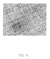
- FIG. 3 shows a SEM image of a stacked carbon nanotube film structure.
- FIG. 4 shows a SEM image of untwisted carbon nanotube wire.
- FIG. 5 shows a SEM image of twisted carbon nanotube wire.
- FIG. 6 shows a flowchart of one embodiment of a method of making electron emission source.
- FIG. 7 shows a cross-section view of another embodiment of an electron emission source.
- FIG. 8 shows a cross-section view of another embodiment of an electron emission device.
- FIG. 9 shows a schematic view of another embodiment of an electron emission device.
- FIG. 10 shows a cross-section view of the electron emission device along a line A-A′ in FIG. 9 .
- FIG. 11 shows a schematic view of one embodiment of an electron emission display.
- FIG. 12 shows an image of display effect of the electron emission display in FIG. 11 .
- FIG. 13 shows a schematic view of another embodiment of an electron emission device.
- FIG. 14 shows a cross-section view of the electron emission device along a line B-B′ in FIG. 13 .
- FIG. 15 shows a schematic view of another embodiment of an electron emission display.
- an electron emission source 10 of one embodiment comprises a first electrode 101 , a semiconductor layer 102 , an electron collection layer 103 , an insulating layer 104 , and a second electrode 105 stacked in that sequence.
- the first electrode 101 is spaced from the second electrode 105 .
- a surface of the first electrode 101 is an electron emission surface to emit electron.
- the electron emission source 10 can be disposed on a substrate 106 , and the second electrode 105 is applied on a surface of the substrate 106 .
- the substrate 106 supports the electron emission source 10 .
- a material of the substrate 106 can glass, quartz, ceramics, diamond, silicon, or other hard plastic materials.
- the material of the substrate 106 can also be resins and other flexible materials.
- the substrate 106 is silica.
- the electron collection layer 103 is sandwiched between the insulating layer 104 and the semiconductor layer 102 .
- the first electrode 101 is located on the semiconductor layer 102 .
- the first electrode 101 is insulated from the second electrode 105 by the insulating layer 104 .
- the electron collection layer 103 collects and storage the electrons.
- the semiconductor layer 102 accelerates the electrons, thus the electrons can have enough energy to escape from the first electrode 101 .
- a material of the insulating layer 104 can be a hard material such as aluminum oxide, silicon nitride, silicon oxide, or tantalum oxide.
- the material of the insulating layer 104 can also be a flexible material such as benzocyclobutene (BCB), acrylic resin, or polyester.
- a thickness of the insulating layer 104 can range from about 50 nanometers to 100 micrometers. In one embodiment, the insulating layer 104 is tantalum oxide with a thickness of 100 nanometers.
- the semiconductor layer 102 is sandwiched between the first electrode 101 and the electron collection layer 103 .
- the semiconductor layer 102 plays a role of accelerating electrons.
- the electrons are accelerated in the semiconductor layer 102 .
- a material of the semiconductor layer 102 can be a semiconductor material, such as zinc sulfide, zinc oxide, magnesium zinc oxide, magnesium sulfide, cadmium sulfide, cadmium selenide, or zinc selenide.
- a thickness of the semiconductor layer 102 can range from about 3 nanometers to about 100 nanometers. In one embodiment, the material of the semiconductor layer 102 is zinc sulfide having a thickness of 50 nanometers.
- the electron collection layer 103 is sandwiched between the semiconductor layer 102 and the insulating layer 104 .
- the electron collection layer 103 is a conductive layer comprising a conductive material.
- the material of the electron collection layer 103 can be gold, platinum, scandium, palladium, hathium, or other metal or metal alloy. Furthermore, the material of the electron collection layer 103 can also be carbon nanotubes or graphene.
- a thickness of the electron collection layer 103 can range from about 10 nanometers to about 1 micrometer.
- the electron collection layer 103 can comprise a carbon nanotube layer.
- the carbon nanotube layer comprises a plurality of carbon nanotubes.
- the carbon nanotubes in the electron collection layer 103 extend parallel to the surface of the electron collection layer 103 .
- the carbon nanotube layer includes a plurality of carbon nanotubes.
- the carbon nanotubes in the carbon nanotube layer can be single-walled, double-walled, or multi-walled carbon nanotubes.
- the length and diameter of the carbon nanotubes can be selected according to need.
- the thickness of the carbon nanotube layer can be in a range from about 10 nm to about 100 ⁇ m, for example, about 10 nm, 100 nm, 200 nm, 1 ⁇ m, 10 ⁇ m or 50 ⁇ m.
- the carbon nanotube layer forms a pattern.
- the patterned carbon nanotube layer defines a plurality of apertures.
- the apertures can be dispersed uniformly.
- the apertures extend throughout the carbon nanotube layer along the thickness direction thereof.
- the aperture can be a hole defined by several adjacent carbon nanotubes, or a gap defined by two substantially parallel carbon nanotubes and extending along axial direction of the carbon nanotubes.
- the size of the aperture can be the diameter of the hole or width of the gap, and the average aperture size can be in a range from about 10 nm to about 500 ⁇ m, for example, about 50 nm, 100 nm, 500 nm, 1 ⁇ m, 10 ⁇ m, 80 ⁇ m or 120 ⁇ m.
- the hole-shaped apertures and the gap-shaped apertures can exist in the patterned carbon nanotube layer at the same time.
- the sizes of the apertures within the same carbon nanotube layer can be different. The smaller the size of the apertures, the less dislocation defects will occur during the process of growing first semiconductor layer 120 . In one embodiment, the sizes of the apertures are in a range from about 10 nm to about 10 ⁇ m.
- the carbon nanotubes of the carbon nanotube layer can be orderly arranged to form an ordered carbon nanotube structure or disorderly arranged to form a disordered carbon nanotube structure.
- disordered carbon nanotube structure includes, but is not limited to, a structure where the carbon nanotubes are arranged along many different directions, and the aligning directions of the carbon nanotubes are random.
- the number of the carbon nanotubes arranged along each different direction can be substantially the same (e.g. uniformly disordered).
- the disordered carbon nanotube structure can be isotropic.
- the carbon nanotubes in the disordered carbon nanotube structure can be entangled with each other.
- ordered carbon nanotube structure includes, but is not limited to, a structure where the carbon nanotubes are arranged in a consistently systematic manner, e.g., the carbon nanotubes are arranged approximately along a same direction and/or have two or more sections within each of which the carbon nanotubes are arranged approximately along a same direction (different sections can have different directions).
- the carbon nanotubes in the carbon nanotube layer are arranged to extend along the direction substantially parallel to the surface of the semiconductor layer 102 . In one embodiment, all the carbon nanotubes in the carbon nanotube layer are arranged to extend along the same direction. In another embodiment, some of the carbon nanotubes in the carbon nanotube layer are arranged to extend along a first direction, and some of the carbon nanotubes in the carbon nanotube layer are arranged to extend along a second direction, perpendicular to the first direction.
- the carbon nanotube layer is a free-standing structure and can be drawn from a carbon nanotube array.
- the term “free-standing structure” means that the carbon nanotube layer can sustain the weight of itself when it is hoisted by a portion thereof without any significant damage to its structural integrity.
- the carbon nanotube layer can be suspended by two spaced supports.
- the free-standing carbon nanotube layer can be laid on the insulating layer 104 directly and easily.
- the carbon nanotube layer can be a substantially pure structure of the carbon nanotubes, with few impurities and chemical functional groups.
- the carbon nanotube layer can be a composite including a carbon nanotube matrix and non-carbon nanotube materials.
- the non-carbon nanotube materials can be graphite, graphene, silicon carbide, boron nitride, silicon nitride, silicon dioxide, diamond, amorphous carbon, metal carbides, metal oxides, or metal nitrides.
- the non-carbon nanotube materials can be coated on the carbon nanotubes of the carbon nanotube layer or filled in the apertures.
- the non-carbon nanotube materials are coated on the carbon nanotubes of the carbon nanotube layer so the carbon nanotubes can have a greater diameter and the apertures can a have smaller size.
- the non-carbon nanotube materials can be deposited on the carbon nanotubes of the carbon nanotube layer by CVD or physical vapor deposition (PVD), such as sputtering.
- the carbon nanotube layer can include at least one carbon nanotube film, at least one carbon nanotube wire, or a combination thereof.
- the carbon nanotube layer can include a single carbon nanotube film or two or more stacked carbon nanotube films.
- the thickness of the carbon nanotube layer can be controlled by the number of the stacked carbon nanotube films.
- the number of the stacked carbon nanotube films can be in a range from about 2 to about 100, for example, about 10, 30, or 50.
- the carbon nanotube layer can include a layer of parallel and spaced carbon nanotube wires.
- the carbon nanotube layer can also include a plurality of carbon nanotube wires crossed or weaved together to form a carbon nanotube net.
- the distance between two adjacent parallel and spaced carbon nanotube wires can be in a range from about 0.1 ⁇ m to about 200 ⁇ m. In one embodiment, the distance between two adjacent parallel and spaced carbon nanotube wires can be in a range from about 10 ⁇ m to about 100 ⁇ m.
- the size of the apertures can be controlled by controlling the distance between two adjacent parallel and spaced carbon nanotube wires.
- the length of the gap between two adjacent parallel carbon nanotube wires can be equal to the length of the carbon nanotube wire. It is understood that any carbon nanotube structure described can be used with all embodiments.
- the carbon nanotube layer includes at least one drawn carbon nanotube film.
- a drawn carbon nanotube film can be drawn from a carbon nanotube array that is able to have a film drawn therefrom.
- the drawn carbon nanotube film includes a plurality of successive and oriented carbon nanotubes joined end-to-end by van der Waals attractive force therebetween.
- the drawn carbon nanotube film is a free-standing film. Referring to FIG. 2 , each drawn carbon nanotube film includes a plurality of successively oriented carbon nanotube segments joined end-to-end by van der Waals attractive force therebetween.
- Each carbon nanotube segment includes a plurality of carbon nanotubes parallel to each other, and combined by van der Waals attractive force therebetween.
- the carbon nanotubes in the drawn carbon nanotube film are oriented along a preferred orientation.
- the drawn carbon nanotube film can be treated with an organic solvent to increase the mechanical strength and toughness, and reduce the coefficient of friction of the drawn carbon nanotube film.
- a thickness of the drawn carbon nanotube film can range from about 0.5 nm to about 100 ⁇ m.
- the carbon nanotube layer can include at least two stacked drawn carbon nanotube films.
- the carbon nanotube layer can include two or more coplanar carbon nanotube films, and each coplanar carbon nanotube film can include multiple layers.
- an angle can exist between the orientation of carbon nanotubes in adjacent films, whether stacked or adjacent. Adjacent carbon nanotube films are combined by the van der Waals attractive force therebetween.
- An angle between the aligned directions of the carbon nanotubes in two adjacent carbon nanotube films can range from about 0 degrees to about 90 degrees.
- the angle between the aligned directions of the carbon nanotubes in adjacent stacked drawn carbon nanotube films is larger than 0 degrees, a plurality of micropores is defined by the carbon nanotube layer.
- the carbon nanotube layer shown with the angle between the aligned directions of the carbon nanotubes in adjacent stacked drawn carbon nanotube films is 90 degrees. Stacking the carbon nanotube films will also add to the structural integrity of the carbon nanotube layer.
- the carbon nanotube wire can be untwisted or twisted. Treating the drawn carbon nanotube film with a volatile organic solvent can form the untwisted carbon nanotube wire. Specifically, the organic solvent is applied to soak the entire surface of the drawn carbon nanotube film. During the soaking, adjacent parallel carbon nanotubes in the drawn carbon nanotube film will bundle together, due to the surface tension of the organic solvent as it volatilizes. Thus, the drawn carbon nanotube film will be shrunk into untwisted carbon nanotube wire.
- the untwisted carbon nanotube wire includes a plurality of carbon nanotubes substantially oriented along a same direction (i.e., a direction along the length of the untwisted carbon nanotube wire).
- the carbon nanotubes are parallel to the axis of the untwisted carbon nanotube wire.
- the untwisted carbon nanotube wire includes a plurality of successive carbon nanotube segments joined end to end by van der Waals attractive force therebetween.
- Each carbon nanotube segment includes a plurality of carbon nanotubes substantially parallel to each other, and combined by van der Waals attractive force therebetween.
- the carbon nanotube segments can vary in width, thickness, uniformity, and shape. Length of the untwisted carbon nanotube wire can be arbitrarily set as desired.
- a diameter of the untwisted carbon nanotube wire ranges from about 0.5 nm to about 100 ⁇ m.
- the twisted carbon nanotube wire can be formed by twisting a drawn carbon nanotube film using a mechanical force to turn the two ends of the drawn carbon nanotube film in opposite directions.
- the twisted carbon nanotube wire includes a plurality of carbon nanotubes helically oriented around an axial direction of the twisted carbon nanotube wire.
- the twisted carbon nanotube wire includes a plurality of successive carbon nanotube segments joined end to end by van der Waals attractive force therebetween.
- Each carbon nanotube segment includes a plurality of carbon nanotubes parallel to each other, and combined by van der Waals attractive force therebetween. Length of the carbon nanotube wire can be set as desired.
- a diameter of the twisted carbon nanotube wire can be from about 0.5 nm to about 100 ⁇ m.
- the twisted carbon nanotube wire can be treated with a volatile organic solvent after being twisted. After being soaked by the organic solvent, the adjacent paralleled carbon nanotubes in the twisted carbon nanotube wire will bundle together, due to the surface tension of the organic solvent when the organic solvent volatilizes. The specific surface area of the twisted carbon nanotube wire will decrease, while the density and strength of the twisted carbon nanotube wire will be increased.
- the electron collection layer 103 can also be a graphene layer.
- the graphene layer can include at least one graphene film.
- the graphene film namely a single-layer graphene, is a single layer of continuous carbon atoms.
- the single-layer graphene is a nanometer-thick two-dimensional analog of fullerenes and carbon nanotubes.
- a plurality of graphene films can be stacked on each other or arranged coplanar side by side.
- the thickness of the graphene layer can be in a range from about 0.34 nanometers to about 10 micrometers.
- the thickness of the graphene layer can be 1 nanometer, 10 nanometers, 200 nanometers, 1 micrometer, or 10 micrometers.
- the single-layer graphene can have a thickness of a single carbon atom.
- the graphene layer is a pure graphene structure consisting of graphene. Because the single-layer graphene has great conductivity, thus the electrons can be easily collected and accelerated to the semiconductor layer 102 .
- the graphene layer can be prepared and transferred to the substrate by graphene powder or graphene film.
- the graphene film can also be prepared by the method of chemical vapor deposition (CVD) method, a mechanical peeling method, electrostatic deposition method, a silicon carbide (SiC) pyrolysis, or epitaxial growth method.
- the graphene powder can prepared by liquid phase separation method, intercalation stripping method, cutting carbon nanotubes, preparation solvothermal method, or organic synthesis method.
- the electron collection layer 103 is a drawn carbon nanotube film having a thickness of 5 nanometers to 50 nanometers.
- the carbon nanotube film has good tensile conductivity and electron collecting effect. Furthermore, the carbon nanotube film has good mechanical properties, which can effectively improve the lifespan of the electron emission source 10 .
- the first electrode 101 is a thin conductive metal film.
- a material of the first electrode 101 can be gold, platinum, scandium, palladium, or hafnium metal.
- the thickness of the first electrode 101 can range from about 10 nanometers to about 100 micrometers, such as 10 nanometers, 50 nanometers.
- the first electrode 101 is molybdenum film having a thickness of 100 nanometers.
- the material of the first electrode 101 may also be carbon nanotube layer or graphene layer.
- the plurality of carbon nanotubes in the carbon nanotube layer form a conductive network.
- the carbon nanotube layer can also define a plurality of apertures. Thus the electrons can be easily escaped from the first electrode 101 .
- the material of the second electrode 105 can be same as the first electrode 101 .
- the electron emission source 10 works in the alternating current (AC) driving mode.
- the working principle of the electron emission source 10 is: in the negative half cycle, the potential of the second electrode 105 is high, and the electrons are injected into the semiconductor layer 102 from the first electrode 101 . While the electrons reach the electron collection layer 103 , the electrons will be collected and stored in the electron collection layer 103 . An interface between the electron collection layer 103 and insulating layer 104 forms an interface state. In the positive half cycle, due to the higher potential of the carbon nanotube layer of the first electrode 101 , the electrons stored on the interface state are pulled to the semiconductor layer 102 and accelerated in the semiconductor layer 102 . Because the semiconductor layer 102 is in contact with the first electrode 101 , a part of high-energy electrons can rapidly pass through the carbon nanotube layer of the first electrode 101 .
- a method of making electron emission source 10 comprises:
- the substrate 106 can be rectangular.
- the material of the substrate 106 can be insulating material such as glass, ceramic, or silicon dioxide.
- the substrate 106 is a silicon dioxide.
- the preparation method of the second electrode 105 can be magnetron sputtering method, vapor deposition method, or an atomic layer deposition method.
- the second electrode 105 is the molybdenum metal film formed by vapor deposition, and the thickness of the second electrode 105 is about 100 nanometers.
- the preparation method of the insulating layer 104 can be the magnetron sputtering method, the vapor deposition method, or the atomic layer deposition method.
- the insulating layer 104 is tantalum oxide formed by atomic layer deposition method, and the thickness of the insulating layer 104 is about 100 nanometers.
- the method of forming the electron collector layer 103 can be selected according to the material. While the material of the electron collector layer 103 is metal or metal alloy, the electron collection layer 103 can be formed by magnetron sputtering, vapor deposition, or atomic layer deposition. While the electron collector layer 103 comprises carbon nanotube layer, the electron collection layer 103 can be formed by directly locating a drawn carbon nanotube film, a flocculate carbon nanotube film, or a pressed carbon nanotube film on the insulating layer 104 . While the material of the electron collector layer 103 is graphene, the electron collection layer 103 can be formed by applying a graphene layer on the insulating layer 104 . In one embodiment, the electron collection layer 103 is formed by directly locating a carbon nanotube film drawn from a carbon nanotube array. The thickness of the electron collector layer 103 ranges from about 5 nanometers to about 50 nanometers.
- the method of forming semiconductor layer 102 can be similar to the method of forming the insulating layer 104 .
- the semiconductor layer 102 is zinc sulfide layer formed by a vapor deposition method, and the thickness of the semiconductor layer 102 is about 50 nanometers.
- step (S15) the method of forming the first electrode 101 can be same as the method of forming the electron collection layer 103 .
- the drawn carbon nanotube film is applied as the first electrode 101 .
- the electron emission source 10 can have the following advantages.
- the electron collection layer 103 is located between the semiconductor layer 102 and the insulating layer 104 , thus the electron collection layer 103 can effectively collect and store the electrons between the semiconductor layer 102 and the insulating layer 104 , and the electron emission efficiency of the electron emission source 10 can be improved compared to the traditional MISM electron emission source.
- an electron emission source 20 of one embodiment comprises a first electrode 101 , a semiconductor layer 102 , an electron collection layer 103 , an insulating layer 104 , and a second electrode 105 stacked in that sequence. Furthermore, a pair of bus electrodes 107 is located on the first electrode 101 .
- the structure of electron emission source 20 is similar to the structure of electron emission source 10 , except that the pair of bus electrodes 107 is located on the first electrode 101 .
- the pair of bus electrodes 107 are spaced from each other and electrically connected to the first electrode 101 in order to supply current.
- Each bus electrode 107 is a bar-shaped electrode.
- the pair of bus electrodes 107 can be applied on the two opposite sides of the first electrode 101 along the extending direction of the carbon nanotubes.
- the extending direction of the bar-shaped bus electrode 107 is perpendicular to the extending direction of the plurality of carbon nanotubes of the first electrode 101 .
- the current can be uniformly distributed in the first electrode 101 .
- a shape of the bus electrode 107 can be bar-shaped, square, triangular, rectangular, etc.
- a material of the bus electrode 107 can be gold, platinum, scandium, palladium, hathium, or metal alloy.
- the bus electrode 107 is bar-shaped platinum electrode.
- the pair of bar-shaped bus electrodes 107 are parallel with and spaced from each other.
- an electron emission device 300 of one embodiment comprises a plurality of electron emission units 30 .
- Each of the plurality of electron emission units 30 comprises a first electrode 101 , a semiconductor layer 102 , an electron collection layer 103 , an insulating layer 104 , and a second electrode 105 stacked in that sequence.
- the insulating layers 104 in the plurality of electron emission units 30 are in contact with each other and form a continuous layer.
- the electron emission device 300 can be located on a substrate 106 .
- the electron emission unit 30 is similar to the electron emission source structure 10 described above, except that the plurality of electron emission units 30 share the common insulating layer 104 .
- the plurality of electron emission units 30 can work independently from each other.
- the first electrodes 101 in adjacent two of the plurality of electron emission units 30 are spaced apart from each other
- the semiconductor layers 102 in adjacent two of the plurality of electron emission units 30 are spaced apart from each other
- the second electrodes 105 in adjacent two of the plurality of electron emission units 30 are also spaced apart from each other.
- a distance between adjacent two semiconductor layers 102 is about 200 nanometers
- a distance between adjacent two first electrodes 101 is about 200 nanometers
- a distance between the adjacent two electrodes 105 is about 200 nanometers.
- An embodiment of a method of making electron emission device 300 comprises:
- the method of making the electron emission device 300 is similar to the method of making the electron emission source 10 , except that the plurality of second electrodes 105 is applied on the substrate 106 and spaced from each other.
- the method of forming the plurality of second electrodes 105 can be screen printing method, magnetron sputtering method, vapor deposition method, atomic layer deposition method.
- the plurality of second electrodes 105 are formed via the vapor deposition method comprising:
- the material of the mask layer can be polymethyl methacrylate (PMMA) or silicone compound (HSQ).
- PMMA polymethyl methacrylate
- HSQ silicone compound
- the size and the position of the openings in the mask layer can be selected according to the requirement of the distribution of the plurality of electron emitting units 30 .
- the material of the second electrode 105 is molybdenum.
- the number of the second electrode 105 is 16, and the number of the electron emission unit 30 is also 16.
- the method for forming the first electrode 101 can be selected according to the material of the first electrode 101 . While the material of the first electrode 101 is conductive metal, the first electrode can be formed by sputtering, atomic layer deposition, vapor deposition method. While the first electrode 101 is graphene or carbon nanotubes, the first electrode 101 can be formed by chemical vapor deposition. The carbon nanotube layer or graphene membrane is etched to form the first electrodes 101 spaced apart.
- the semiconductor layer preform can be patterned via plasma etching, laser etching, or wet etching. In one embodiment, the semiconductor layer preform is patterned according to the distribution of the first electrode 101 .
- each of the plurality of electron emission units 30 comprises one electrode 101 , one semiconductor layer 102 , and one second electrode 105 .
- the electron collection layer 103 can also be patterned.
- the first electrode 101 , the semiconductor layer 102 , the electron collection layer 103 , and the second electrode 105 in the plurality of electron emission units 30 are spaced from each other.
- the plurality of electron emission units 30 share common insulating layer 104 .
- the electron collection layer 103 can be patterned by plasma etching method, laser etching method, or wet etching method.
- an electron emission device 400 of one embodiment comprises a plurality of electron emission units 40 , a plurality of row electrodes 401 , and a plurality of column electrodes 402 on a substrate 106 .
- Each of the plurality of electron emission units 40 comprises a first electrode 101 , a semiconductor layer 102 , an electron collection layer 103 , an insulating layer 104 , and a second electrode 105 stacked in that sequence.
- the insulating layers 104 in the plurality of electron emission units 40 are connected with each other to form a continuous layered structure.
- the electron emission device 400 is similar to the electron emission device 300 , except that the electron emission device 400 further comprises the plurality of row electrodes 401 and the plurality of column electrodes 402 electrically connected to the plurality of electron emission units 40 .
- the plurality of row electrodes 401 is parallel with and spaced from each other.
- the plurality of column electrodes 402 are parallel with and spaced from each other.
- the plurality of column electrodes 402 are insulated from the plurality of row electrodes 402 through the insulating layer 104 .
- the adjacent two row electrodes 401 are intersected with the adjacent two row electrodes 401 to form a grid.
- a section is defined between the adjacent two row electrodes 401 and the adjacent two column electrodes 402 .
- the electron emission unit 40 is received in one of sections and electrically connected to the row electrode 401 and the column electrode 402 .
- the row electrode 401 and the column electrode 402 can electrically connect to the electron emission unit 40 via two electrode leads 403 respectively to supply current for the electron emission unit 40 .
- the plurality of column electrodes 402 are perpendicular to the plurality of row electrodes 401 .
- the plurality of electron emission units 40 form an array with a plurality of rows and columns.
- the plurality of first electrodes 101 in the plurality of electron emission units 40 are spaced apart from each other.
- the plurality of second electrodes 105 in the plurality of electron emission units 40 are also spaced apart from each other.
- the plurality of semiconductor layers 102 in the plurality of electron emission units 40 can be spaced apart from each other.
- the plurality of electron collection layer 103 in the plurality of electron emission units 40 can connect to each other to form an integrated structure. It means that the plurality of electron collection layer 103 form a continuous layered structure, and the plurality of electron emission units 40 share a common electron collection layer 103 .
- an electron emission display 500 of one embodiment comprises a substrate 106 , a plurality of electron emission units 40 on the substrate 106 , and an anode structure 510 .
- the plurality of electron emission units 40 are spaced from the anode structure 510 and face to the anode structure 510 .
- the anode structure 510 comprises a glass substrate 512 , an anode 514 on the glass substrate 512 , and phosphor layer 516 coated on the anode 514 .
- the anode structure 510 is supported by an insulating support 518 .
- the substrate 106 , the glass substrate 512 , and the insulating support 518 form a sealed space.
- the anode 514 can be indium tin oxide (ITO) film.
- the phosphor layer 516 face to the plurality of electron emission units 40 .
- the phosphor layer 516 face to the first electrode 101 to receive electrons emitted from the first electrode 101 .
- different voltages are applied to the first electrode 101 , the second electrode 105 , and the anode 514 of the electron emission display 500 .
- the second electrode 105 is at the ground or zero voltage
- the voltage applied on the first electrode 101 is several tens of volts
- the voltage applied on the anode 514 is a few hundred volts.
- the electrons emitted from the first electrode 101 of the electron emission unit 40 are driven under the electric filed to move toward the phosphor layer 516 .
- the electrons eventually reaches the anode structure 510 and bombarded the phosphor layer 516 coated on the anode 514 .
- fluorescence can be activated from the phosphor layer 516 .
- the electrons in the electron emission display 500 are uniformly emitted, and the electron emission display 500 has better luminous intensity.
- an electron emission device 600 of one embodiment comprises a plurality of first electrodes 1010 spaced from each other, a plurality of second electrodes 1050 spaced from each other.
- the plurality of first electrodes 1010 are bar-shaped and extend along a first direction
- the plurality of second electrodes 1050 are bar-shaped and extend along a second direction that intersects with the first direction.
- the plurality of first electrodes 1010 are intersected with the plurality of second electrodes 1050 .
- a semiconductor layer 102 , an electron collection layer 103 , and an insulating layer 104 are stacked together and sandwiched between the first electrode 1010 and the second electrode 1050 at intersections of the first electrode 1010 and the second electrode 1050 .
- the first electrode 1010 is located on the semiconductor layer 102 .
- the electron emission device 600 is similar to the electron emission device 400 , except that the electron emission device 600 comprises the plurality of bar-shaped first electrodes 1010 and the plurality of bar-shaped second electrodes 1050 .
- the first direction can be defined as the X direction
- the second direction can be defined as the Y direction that intersects with the X direction
- the Z direction is defined as a third direction perpendicular to both the X direction and Y direction.
- the plurality of first electrodes 1010 are aligned along a plurality of rows
- the plurality of second electrodes 1050 are aligned along a plurality of columns.
- An electron emission unit 60 is formed at each intersection in the electron emission device 600 .
- the electron emission unit 60 comprises the semiconductor layer 102 , the electron collection layer 103 , and the insulating layer 104 sandwiched between the first electrode 1010 and the second electrode 1050 at the intersection, and the semiconductor layer 102 is in contact with the first electrode 1010 .
- the plurality of electron emission units 60 can be spaced from each other and aligned along a plurality of rows and a plurality of columns.
- the semiconductor layers 102 in the plurality of electron emission units 60 are also spaced apart from each other.
- the plurality of semiconductor layers 102 aligned along the same row are electrically connected to the same first electrode 101 .
- the plurality of semiconductor layers 102 aligned along the same column are electrically connected to the same second electrode 105 .
- the plurality of electron emission units 60 aligned along the same rows share the same first electrode 101
- the plurality of electron emission units 60 aligned along the same columns share the same second electrode 105 .
- the plurality of electron emission units 60 can share a common electron collection layer 103 .
- the plurality of electron emission units 60 can also share a common insulating layer 104 .
- the electron collection layer 103 in the plurality of electron emission units 60 are spaced apart from each other, and the insulating layer 104 in the plurality of electron emission units 60 are also spaced apart from each other.
- the electrons can be emitted from each of the plurality of electron emission units 60 at the intersections.
- the second electrode 1050 can be applied with a ground or zero voltage, the voltage applied on the first electrode 1010 can be tens of volts to hundreds of volts.
- An electric field is formed between the first electrode 1010 and the second electrode 1050 at the intersection. The electrons pass through the semiconductor layer 102 and emit from the first electrode 1010 .
- An embodiment of a method of making electron emission device 600 comprises:
- the method of making electron emission device 600 in present embodiment is similar to the method of making electron emission device 300 .
- the first direction can be intersected with the second direction.
- the electron collection layer 103 and the insulating layer 104 can also be patterned according the patterned structure of the first electrode 1010 .
- an electron emission display 700 of one embodiment comprises a substrate 106 , an electron emission device 600 located on the substrate 106 , and an anode structure 510 spaced from the electron emission device 600 .
- the electron emission device 600 comprises a plurality of electron emission units 60 .
- the electron emission display 700 is similar to the electron emission display 500 , except that the plurality of first electrodes 101 are connected with each other to form a plurality of bar-shaped first electrodes 1010 along a first direction. Furthermore, the plurality of second electrodes 105 are connected with each other to form the plurality of second electrodes 1050 along a second direction.
- fluorescence is generated from the electron emission display 700 .
Abstract
Description
Claims (18)
Applications Claiming Priority (3)
| Application Number | Priority Date | Filing Date | Title |
|---|---|---|---|
| CN201410024559.8 | 2014-01-20 | ||
| CN201410024559.8A CN104795298B (en) | 2014-01-20 | 2014-01-20 | Electron emission device and display |
| CN201410024559 | 2014-01-20 |
Publications (2)
| Publication Number | Publication Date |
|---|---|
| US20150206697A1 US20150206697A1 (en) | 2015-07-23 |
| US9378920B2 true US9378920B2 (en) | 2016-06-28 |
Family
ID=53545416
Family Applications (1)
| Application Number | Title | Priority Date | Filing Date |
|---|---|---|---|
| US14/600,000 Active US9378920B2 (en) | 2014-01-20 | 2015-01-19 | Electron emission device and electron emission display |
Country Status (4)
| Country | Link |
|---|---|
| US (1) | US9378920B2 (en) |
| JP (1) | JP5818937B2 (en) |
| CN (1) | CN104795298B (en) |
| TW (1) | TWI534846B (en) |
Families Citing this family (8)
| Publication number | Priority date | Publication date | Assignee | Title |
|---|---|---|---|---|
| CN104795292B (en) * | 2014-01-20 | 2017-01-18 | 清华大学 | Electron emission device, manufacturing method thereof and display |
| CN104795300B (en) * | 2014-01-20 | 2017-01-18 | 清华大学 | Electron emission source and manufacturing method thereof |
| CN104795297B (en) * | 2014-01-20 | 2017-04-05 | 清华大学 | Electron emitting device and electron emission display device |
| CN104795294B (en) * | 2014-01-20 | 2017-05-31 | 清华大学 | Electron emitting device and electron emission display device |
| CN104795296B (en) * | 2014-01-20 | 2017-07-07 | 清华大学 | Electron emitting device and display |
| CN104795295B (en) * | 2014-01-20 | 2017-07-07 | 清华大学 | Electron emission source |
| CN104795293B (en) * | 2014-01-20 | 2017-05-10 | 清华大学 | Electron emission source |
| CN104795291B (en) * | 2014-01-20 | 2017-01-18 | 清华大学 | Electron emission device, manufacturing method thereof and display |
Citations (30)
| Publication number | Priority date | Publication date | Assignee | Title |
|---|---|---|---|---|
| JPH10241553A (en) | 1997-02-25 | 1998-09-11 | Yamaha Corp | Cold cathode type field emission element and its manufacture |
| JPH1167065A (en) | 1997-08-08 | 1999-03-09 | Pioneer Electron Corp | Electron emitting element and display device using the same |
| TW518632B (en) | 2001-10-08 | 2003-01-21 | Ind Tech Res Inst | Manufacturing process of cathode plate for nano carbon tube field emission display |
| US20040085010A1 (en) * | 2002-06-24 | 2004-05-06 | Ngk Insulators, Ltd. | Electron emitter, drive circuit of electron emitter and method of driving electron emitter |
| US20050116214A1 (en) * | 2003-10-31 | 2005-06-02 | Mammana Victor P. | Back-gated field emission electron source |
| US20050145835A1 (en) * | 2003-03-15 | 2005-07-07 | Samsung Electronics Co., Ltd. | Emitter for electron-beam projection lithography system and manufacturing method thereof |
| US20060138933A1 (en) * | 2004-11-29 | 2006-06-29 | Yoo Seung J | Electron emission display |
| US20060186786A1 (en) * | 2003-04-21 | 2006-08-24 | Tadashi Iwamatsu | Electron emitting element and image forming apparatus employing it |
| US20060291905A1 (en) * | 2003-06-13 | 2006-12-28 | Hiroyuki Hirakawa | Electron emitter, charger, and charging method |
| US20070018552A1 (en) * | 2005-07-21 | 2007-01-25 | Samsung Sdi Co., Ltd. | Electron emission device, electron emission type backlight unit and flat display apparatus having the same |
| US20080211401A1 (en) * | 2004-12-17 | 2008-09-04 | Tomonari Nakada | Electron Emission Device And Manufacturing Method Of The Same |
| US20080248310A1 (en) * | 2007-04-04 | 2008-10-09 | Samsung Sdi Co., Ltd. | Carbon nanotube hybrid system using carbide-derived carbon, a method of making the same, an electron emitter comprising the same, and an electron emission device comprising the electron emitter |
| CN100530744C (en) | 2006-07-06 | 2009-08-19 | 西安交通大学 | Structure of organic solar cell and organic solar cell produced with the same structure |
| US20100039014A1 (en) * | 2008-08-14 | 2010-02-18 | Seoul National University Research & Development Business Foundation (Snu R&Db Foundation) | Electron multipliers |
| US20100215402A1 (en) * | 2009-02-24 | 2010-08-26 | Ayae Nagaoka | Electron emitting element, electron emitting device, light emitting device, image display device, air blowing device, cooling device, charging device, image forming apparatus, electron-beam curing device, and method for producing electron emitting element |
| US20110169276A1 (en) * | 2008-06-16 | 2011-07-14 | Norio Akamatsu | Field effect power generation device |
| US20110221328A1 (en) * | 2007-02-12 | 2011-09-15 | Nemanich Robert J | Thermionic Electron Emitters/Collectors Have a Doped Diamond Layer with Variable Doping Concentrations |
| US20110254431A1 (en) * | 2010-04-14 | 2011-10-20 | Hiroyuki Hirakawa | Electron emitting element and method for producing the same |
| US20120074874A1 (en) * | 2010-02-24 | 2012-03-29 | Kanako Hirata | Electron emitting element, devices utilizing said element, and method for producing said element |
| TW201222863A (en) | 2010-10-01 | 2012-06-01 | Applied Materials Inc | High efficiency solar cell device with gallium arsenide absorber layer |
| TW201314986A (en) | 2011-07-20 | 2013-04-01 | Sumitomo Chemical Co | Display device and method for manufacturing the same |
| TW201339087A (en) | 2012-03-21 | 2013-10-01 | Hon Hai Prec Ind Co Ltd | Preparation of semiconducting single-walled carbon nanotube |
| US20150206689A1 (en) * | 2014-01-20 | 2015-07-23 | Tsinghua University | Electron emission source |
| US20150206692A1 (en) * | 2014-01-20 | 2015-07-23 | Tsinghua University | Electron emission device and electron emission display |
| US20150206691A1 (en) * | 2014-01-20 | 2015-07-23 | Tsinghua University | Electron emission device and electron emission display |
| US20150206694A1 (en) * | 2014-01-20 | 2015-07-23 | Tsinghua University | Electron emission device and electron emission display |
| US20150206695A1 (en) * | 2014-01-20 | 2015-07-23 | Tsinghua University | Electron emission source and method for making the same |
| US20150206696A1 (en) * | 2014-01-20 | 2015-07-23 | Tsinghua University | Electron emission device and electron emission display |
| US20150206693A1 (en) * | 2014-01-20 | 2015-07-23 | Tsinghua University | Electron emission source |
| US20150206699A1 (en) * | 2014-01-20 | 2015-07-23 | Tsinghua University | Electron emission device and electron emission display |
Family Cites Families (7)
| Publication number | Priority date | Publication date | Assignee | Title |
|---|---|---|---|---|
| CN1137501C (en) * | 1998-10-22 | 2004-02-04 | 先锋电子株式会社 | Electron emission device and display device using such electron emission device |
| US6822380B2 (en) * | 2001-10-12 | 2004-11-23 | Hewlett-Packard Development Company, L.P. | Field-enhanced MIS/MIM electron emitters |
| WO2006006423A1 (en) * | 2004-07-08 | 2006-01-19 | Pioneer Corporation | Electron emission device, and driving method thereof |
| CN1790587A (en) * | 2004-12-17 | 2006-06-21 | 上海广电电子股份有限公司 | Field emission cathode |
| KR100695111B1 (en) * | 2005-06-18 | 2007-03-14 | 삼성에스디아이 주식회사 | Ferroelectric cold cathode and ferroelectric field emission device comprising the same |
| CN101714496B (en) * | 2009-11-10 | 2014-04-23 | 西安交通大学 | Flat gas excitation light source utilizing multilayer thin film type electron source |
| CN102280332B (en) * | 2011-07-04 | 2013-07-24 | 四川大学 | MIPM (multum in parvo mapping)-type internal field emitting cathode |
-
2014
- 2014-01-20 CN CN201410024559.8A patent/CN104795298B/en active Active
- 2014-02-25 TW TW103106199A patent/TWI534846B/en active
- 2014-04-14 JP JP2014082607A patent/JP5818937B2/en active Active
-
2015
- 2015-01-19 US US14/600,000 patent/US9378920B2/en active Active
Patent Citations (32)
| Publication number | Priority date | Publication date | Assignee | Title |
|---|---|---|---|---|
| JPH10241553A (en) | 1997-02-25 | 1998-09-11 | Yamaha Corp | Cold cathode type field emission element and its manufacture |
| JPH1167065A (en) | 1997-08-08 | 1999-03-09 | Pioneer Electron Corp | Electron emitting element and display device using the same |
| TW518632B (en) | 2001-10-08 | 2003-01-21 | Ind Tech Res Inst | Manufacturing process of cathode plate for nano carbon tube field emission display |
| US20040085010A1 (en) * | 2002-06-24 | 2004-05-06 | Ngk Insulators, Ltd. | Electron emitter, drive circuit of electron emitter and method of driving electron emitter |
| US20050145835A1 (en) * | 2003-03-15 | 2005-07-07 | Samsung Electronics Co., Ltd. | Emitter for electron-beam projection lithography system and manufacturing method thereof |
| US20060186786A1 (en) * | 2003-04-21 | 2006-08-24 | Tadashi Iwamatsu | Electron emitting element and image forming apparatus employing it |
| US20060291905A1 (en) * | 2003-06-13 | 2006-12-28 | Hiroyuki Hirakawa | Electron emitter, charger, and charging method |
| US20050116214A1 (en) * | 2003-10-31 | 2005-06-02 | Mammana Victor P. | Back-gated field emission electron source |
| US20060138933A1 (en) * | 2004-11-29 | 2006-06-29 | Yoo Seung J | Electron emission display |
| US20080211401A1 (en) * | 2004-12-17 | 2008-09-04 | Tomonari Nakada | Electron Emission Device And Manufacturing Method Of The Same |
| US20070018552A1 (en) * | 2005-07-21 | 2007-01-25 | Samsung Sdi Co., Ltd. | Electron emission device, electron emission type backlight unit and flat display apparatus having the same |
| CN100530744C (en) | 2006-07-06 | 2009-08-19 | 西安交通大学 | Structure of organic solar cell and organic solar cell produced with the same structure |
| US20110221328A1 (en) * | 2007-02-12 | 2011-09-15 | Nemanich Robert J | Thermionic Electron Emitters/Collectors Have a Doped Diamond Layer with Variable Doping Concentrations |
| US20080248310A1 (en) * | 2007-04-04 | 2008-10-09 | Samsung Sdi Co., Ltd. | Carbon nanotube hybrid system using carbide-derived carbon, a method of making the same, an electron emitter comprising the same, and an electron emission device comprising the electron emitter |
| US20110169276A1 (en) * | 2008-06-16 | 2011-07-14 | Norio Akamatsu | Field effect power generation device |
| US20100039014A1 (en) * | 2008-08-14 | 2010-02-18 | Seoul National University Research & Development Business Foundation (Snu R&Db Foundation) | Electron multipliers |
| US20100215402A1 (en) * | 2009-02-24 | 2010-08-26 | Ayae Nagaoka | Electron emitting element, electron emitting device, light emitting device, image display device, air blowing device, cooling device, charging device, image forming apparatus, electron-beam curing device, and method for producing electron emitting element |
| US20120074874A1 (en) * | 2010-02-24 | 2012-03-29 | Kanako Hirata | Electron emitting element, devices utilizing said element, and method for producing said element |
| US20110254431A1 (en) * | 2010-04-14 | 2011-10-20 | Hiroyuki Hirakawa | Electron emitting element and method for producing the same |
| US8846437B2 (en) | 2010-10-01 | 2014-09-30 | Applied Materials, Inc. | High efficiency thin film transistor device with gallium arsenide layer |
| TW201222863A (en) | 2010-10-01 | 2012-06-01 | Applied Materials Inc | High efficiency solar cell device with gallium arsenide absorber layer |
| TW201314986A (en) | 2011-07-20 | 2013-04-01 | Sumitomo Chemical Co | Display device and method for manufacturing the same |
| TW201339087A (en) | 2012-03-21 | 2013-10-01 | Hon Hai Prec Ind Co Ltd | Preparation of semiconducting single-walled carbon nanotube |
| US9136117B2 (en) | 2012-03-21 | 2015-09-15 | Tsinghua University | Method for making semiconducting single wall carbon nanotubes |
| US20150206689A1 (en) * | 2014-01-20 | 2015-07-23 | Tsinghua University | Electron emission source |
| US20150206692A1 (en) * | 2014-01-20 | 2015-07-23 | Tsinghua University | Electron emission device and electron emission display |
| US20150206691A1 (en) * | 2014-01-20 | 2015-07-23 | Tsinghua University | Electron emission device and electron emission display |
| US20150206694A1 (en) * | 2014-01-20 | 2015-07-23 | Tsinghua University | Electron emission device and electron emission display |
| US20150206695A1 (en) * | 2014-01-20 | 2015-07-23 | Tsinghua University | Electron emission source and method for making the same |
| US20150206696A1 (en) * | 2014-01-20 | 2015-07-23 | Tsinghua University | Electron emission device and electron emission display |
| US20150206693A1 (en) * | 2014-01-20 | 2015-07-23 | Tsinghua University | Electron emission source |
| US20150206699A1 (en) * | 2014-01-20 | 2015-07-23 | Tsinghua University | Electron emission device and electron emission display |
Also Published As
| Publication number | Publication date |
|---|---|
| TWI534846B (en) | 2016-05-21 |
| JP2015138776A (en) | 2015-07-30 |
| CN104795298B (en) | 2017-02-22 |
| TW201530600A (en) | 2015-08-01 |
| CN104795298A (en) | 2015-07-22 |
| JP5818937B2 (en) | 2015-11-18 |
| US20150206697A1 (en) | 2015-07-23 |
Similar Documents
| Publication | Publication Date | Title |
|---|---|---|
| US9373476B2 (en) | Electron emission device and electron emission display | |
| US9275821B2 (en) | Electron emission device and electron emission display | |
| US9362079B2 (en) | Electron emission source and method for making the same | |
| US9390878B2 (en) | Electron emission source | |
| US9362080B2 (en) | Electron emission device and electron emission display | |
| US9373475B2 (en) | Electron emission source | |
| US9269523B2 (en) | Electron emission device and electron emission display | |
| US9373477B2 (en) | Electron emission device and electron emission display | |
| US9378920B2 (en) | Electron emission device and electron emission display |
Legal Events
| Date | Code | Title | Description |
|---|---|---|---|
| AS | Assignment |
Owner name: TSINGHUA UNIVERSITY, CHINA Free format text: ASSIGNMENT OF ASSIGNORS INTEREST;ASSIGNORS:LIU, PENG;LI, DE-JIE;ZHANG, CHUN-HAI;AND OTHERS;REEL/FRAME:034781/0370 Effective date: 20141228 Owner name: HON HAI PRECISION INDUSTRY CO., LTD., TAIWAN Free format text: ASSIGNMENT OF ASSIGNORS INTEREST;ASSIGNORS:LIU, PENG;LI, DE-JIE;ZHANG, CHUN-HAI;AND OTHERS;REEL/FRAME:034781/0370 Effective date: 20141228 |
|
| STCF | Information on status: patent grant |
Free format text: PATENTED CASE |
|
| MAFP | Maintenance fee payment |
Free format text: PAYMENT OF MAINTENANCE FEE, 4TH YEAR, LARGE ENTITY (ORIGINAL EVENT CODE: M1551); ENTITY STATUS OF PATENT OWNER: LARGE ENTITY Year of fee payment: 4 |
|
| MAFP | Maintenance fee payment |
Free format text: PAYMENT OF MAINTENANCE FEE, 8TH YEAR, LARGE ENTITY (ORIGINAL EVENT CODE: M1552); ENTITY STATUS OF PATENT OWNER: LARGE ENTITY Year of fee payment: 8 |