US9362041B2 - Common mode filter - Google Patents

Common mode filter Download PDF

Info

Publication number
US9362041B2
US9362041B2 US14/045,393 US201314045393A US9362041B2 US 9362041 B2 US9362041 B2 US 9362041B2 US 201314045393 A US201314045393 A US 201314045393A US 9362041 B2 US9362041 B2 US 9362041B2
Authority
US
United States
Prior art keywords
wound
wires
turn
wire
sparsely
Prior art date
Legal status (The legal status is an assumption and is not a legal conclusion. Google has not performed a legal analysis and makes no representation as to the accuracy of the status listed.)
Active, expires
Application number
US14/045,393
Other versions
US20140097928A1 (en
Inventor
Toshio Tomonari
Tsutomu Kobayashi
Kazunori Arimitsu
Current Assignee (The listed assignees may be inaccurate. Google has not performed a legal analysis and makes no representation or warranty as to the accuracy of the list.)
TDK Corp
Original Assignee
TDK Corp
Priority date (The priority date is an assumption and is not a legal conclusion. Google has not performed a legal analysis and makes no representation as to the accuracy of the date listed.)
Filing date
Publication date
Application filed by TDK Corp filed Critical TDK Corp
Assigned to TDK CORPORATION reassignment TDK CORPORATION ASSIGNMENT OF ASSIGNORS INTEREST (SEE DOCUMENT FOR DETAILS). Assignors: ARIMITSU, KAZUNORI, KOBAYASHI, TSUTOMU, TOMONARI, TOSHIO
Publication of US20140097928A1 publication Critical patent/US20140097928A1/en
Priority to US15/142,437 priority Critical patent/US10037844B2/en
Application granted granted Critical
Publication of US9362041B2 publication Critical patent/US9362041B2/en
Priority to US16/011,887 priority patent/US10522283B2/en
Priority to US16/690,691 priority patent/US10755848B2/en
Priority to US16/928,407 priority patent/US10910144B2/en
Priority to US17/141,695 priority patent/US11545296B2/en
Priority to US18/072,845 priority patent/US20230095851A1/en
Active legal-status Critical Current
Adjusted expiration legal-status Critical

Links

Images

Classifications

    • HELECTRICITY
    • H01ELECTRIC ELEMENTS
    • H01FMAGNETS; INDUCTANCES; TRANSFORMERS; SELECTION OF MATERIALS FOR THEIR MAGNETIC PROPERTIES
    • H01F27/00Details of transformers or inductances, in general
    • H01F27/28Coils; Windings; Conductive connections
    • H01F27/2823Wires
    • HELECTRICITY
    • H01ELECTRIC ELEMENTS
    • H01FMAGNETS; INDUCTANCES; TRANSFORMERS; SELECTION OF MATERIALS FOR THEIR MAGNETIC PROPERTIES
    • H01F1/00Magnets or magnetic bodies characterised by the magnetic materials therefor; Selection of materials for their magnetic properties
    • H01F1/01Magnets or magnetic bodies characterised by the magnetic materials therefor; Selection of materials for their magnetic properties of inorganic materials
    • H01F1/03Magnets or magnetic bodies characterised by the magnetic materials therefor; Selection of materials for their magnetic properties of inorganic materials characterised by their coercivity
    • H01F1/032Magnets or magnetic bodies characterised by the magnetic materials therefor; Selection of materials for their magnetic properties of inorganic materials characterised by their coercivity of hard-magnetic materials
    • H01F1/04Magnets or magnetic bodies characterised by the magnetic materials therefor; Selection of materials for their magnetic properties of inorganic materials characterised by their coercivity of hard-magnetic materials metals or alloys
    • H01F1/047Alloys characterised by their composition
    • HELECTRICITY
    • H01ELECTRIC ELEMENTS
    • H01FMAGNETS; INDUCTANCES; TRANSFORMERS; SELECTION OF MATERIALS FOR THEIR MAGNETIC PROPERTIES
    • H01F17/00Fixed inductances of the signal type 
    • H01F17/04Fixed inductances of the signal type  with magnetic core
    • H01F17/045Fixed inductances of the signal type  with magnetic core with core of cylindric geometry and coil wound along its longitudinal axis, i.e. rod or drum core
    • HELECTRICITY
    • H01ELECTRIC ELEMENTS
    • H01FMAGNETS; INDUCTANCES; TRANSFORMERS; SELECTION OF MATERIALS FOR THEIR MAGNETIC PROPERTIES
    • H01F27/00Details of transformers or inductances, in general
    • H01F27/24Magnetic cores
    • HELECTRICITY
    • H01ELECTRIC ELEMENTS
    • H01FMAGNETS; INDUCTANCES; TRANSFORMERS; SELECTION OF MATERIALS FOR THEIR MAGNETIC PROPERTIES
    • H01F27/00Details of transformers or inductances, in general
    • H01F27/28Coils; Windings; Conductive connections

Definitions

  • the present invention relates to a common mode filter, and more particularly relates to a common mode filter configured by using a drum core.
  • a toroidal core or a drum core is used as a specific structure of the common mode filter.
  • a leakage flux can be suppressed as compared to the case of using the drum core, and therefore high noise-removal performance can be obtained.
  • automatic coil winding is difficult for the toroidal core, it inevitably requires manual coil winding, thereby increasing variations in characteristics of the common mode filter.
  • an automatic coil winding method can be used, thereby lessening variations in characteristics of the common mode filter. Further, because the automatic coil winding method can be utilized, a drum-core type common mode filter is suitable for mass production.
  • Japanese Patent Nos. 4789076 and 3973028 disclose an example of a common mode filter configured by using a drum core.
  • two wires each of which constitutes an inductance are wound with a double-layer structure.
  • two wires each of which constitutes an inductance are wound together as a pair of wires.
  • the former winding method is referred to as “layer winding”
  • the latter winding method is referred to as “bifilar winding”.
  • Japanese Patent No. 4737268 discloses an example of an automatic coil winder that is used to wind a wire around a drum core.
  • Ethernet has been widely adopted as an in-vehicle LAN.
  • a common mode filter used in in-vehicle Ethernet is required to have more stable characteristics and higher noise-reduction performance than ever before.
  • a drum-core type common mode filter has a feature of being able to lessen variations in its characteristics, as described above. Therefore, when noise-reduction performance of the drum-core type common mode filter can be improved, it is possible to obtain the optimized common mode filter for in-vehicle Ethernet.
  • mode conversion characteristics which indicate the rate of a differential signal component, input to a common mode filter, to be converted into a common mode noise and to be output.
  • Capacitance between different turns a capacitance caused between different turns
  • the capacitance between different turns can be reduced by providing a given space (a “b” portion in FIG. 2 in Japanese Patent No. 3973028) between pairs of wires wound by bifilar winding.
  • a winding method is employed in Japanese Patent No. 3973028 for the purpose of increasing a cutoff frequency, and there is no description of the mode conversion characteristics in Japanese Patent No. 3973028.
  • each of spaces of equal width is provided between any two adjacent turns, and therefore the number of windings is decreased.
  • the actual number of windings in the common mode filter in Japanese Patent No. 3973028 is only four turns, and an inductance (300 ⁇ H), required for a common mode filter utilized in in-vehicle Ethernet, cannot be obtained from the four turns.
  • an object of the present invention is to provide a drum-core type common mode filter that can realize a high inductance, while achieving reduction in mode conversion characteristics by reducing a capacitance between different turns.
  • a common mode filter of the present invention comprises a drum core that includes a winding core portion and a pair of flange portions provided at both ends of the winding core portion, and first and second wires that are wound around the winding core portion so as to form a pair-wire for each turn, wherein the first and second wires include one or a plurality of sparsely-wound portions in which the first and second wires are wound with adjacent pair-wires spaced from each other, and one or a plurality of closely-wound portions in which the first and second wires are wound with adjacent pair-wires in close contact with each other.
  • the present inventors have found that in view of reducing mode conversion characteristics, sufficient reduction in a capacity between different turns can be achieved by providing a space between only a part of adjacent pair-wires, without having a configuration in which a space is provided between each of adjacent pair-wires as disclosed in Japanese Patent No. 3973028.
  • the present invention is based on these new findings, in which while the one or plurality of sparsely-wound portions are provided to reduce the mode conversion characteristics, the one or plurality of closely-wound portions are provided to enable a higher inductance to be obtained as compared to the case where a space is provided between each of adjacent pair-wires.
  • the first and second wires can be wound in order that a relationship between the number of each of the pair-wires counted from one of the pair of flange portions and arrangement of the one or plurality of sparsely-wound portions, and a relationship between the number of each of the pair-wires counted from the other flange portion and arrangement of the one or plurality of sparsely-wound portions are substantially the same with each other.
  • the mounting directionality can be reduced.
  • the one or the plurality of sparsely-wound portions can include a first sparsely-wound portion
  • the one or the plurality of closely-wound portions can include first and second closely-wound portions
  • the first sparsely-wound portion can be arranged between the first and second closely-wound portions.
  • the first and second wires can be wound by layer winding in which the second wire is wound as a first layer, and the first layer is wound as a second wire, and the first and second wires can be wound in order that a relationship between the number of each of the pair-wires counted from one of the pair of flange portions and a position at which the first wire falls to the first layer at an end of the first closely-wound portion, and a relationship between the number of each of the pair-wires counted from the other flange portion and a position at which the first wire falls to the first layer at an end of the second closely-wound portion are substantially the same with each other.
  • the mounting directionality can further be reduced.
  • the first and second wires are wound by bifilar winding, and the first and second wires can cross each other within the first sparsely-wound portion.
  • the polarities are opposite to each other on both sides of the first sparsely-wound portion, and therefore it is possible to balance the polarities.
  • the one or the plurality of sparsely-wound portions can include first and second sparsely-wound portions
  • the one or the plurality of closely-wound portions can include a first closely-wound portion
  • the first closely-wound portion can be arranged between the first and second sparsely-wound portions.
  • the one or the plurality of closely-wound portions further can include second and third closely-wound portions, and the first and second sparsely-wound portions and the first to third closely-wound portions can be arranged from one of the pair of flange portions to the other flange portion in order of the second closely-wound portion, the first sparsely-wound portion, the first closely-wound portion, the second sparsely-wound portion, and the third closely-wound portion.
  • each of the first and second sparsely-wound portions can include a predetermined number of the pair-wires, distances between the adjacent pair-wires in the first sparsely-wound portion can be increasingly shorter in order from a position closer to one of the pair of flange portions, and distances between the adjacent pair-wires in the second sparsely-wound portion can be increasingly shorter in order from a position closer to the other flange portion.
  • the width of spaces is increasingly larger as the spaces are positioned closer to both ends of the winding core portion, which have a large influence on reducing the mode conversion characteristics, and therefore it is possible to reduce the capacitance between different turns efficiently.
  • the first and second wires can be wound by layer winding. With this configuration, it is possible to increase the number of windings as compared to the case of bifilar winding. Certainly, in each of the above common mode filters, the first and second wires can also be wound by bifilar winding.
  • one or a plurality of sparsely-wound portions are provided to achieve reduction in mode conversion characteristics
  • one or a plurality of closely-wound portions are provided to enable a higher inductance to be obtained as compared to the case where a space is provided between each of adjacent pair-wires.
  • FIG. 1 is a schematic perspective view of an exterior structure of a surface-mount common mode filter according to a first embodiment of the present invention
  • FIGS. 2A to 2D are plan views of the common mode filter shown in FIG. 1 with a plate core removed, when viewed respectively from four directions in an x-z plane;
  • FIG. 3 is an electric circuit diagram realized by the common mode filter shown in FIG. 1 ;
  • FIG. 4 is a schematic diagram showing a winding state of the wires in the common mode filter shown in FIG. 1 ;
  • FIGS. 5A and 5B are explanatory diagrams of a winding method of the wires shown in FIG. 4 ;
  • FIG. 6 is a schematic diagram showing a modification of the winding state of the wires shown in FIG. 4 ;
  • FIG. 7 is a schematic diagram showing a winding state of the wires in the common mode filter according to a second embodiment of the present invention.
  • FIG. 8 is a schematic diagram showing a modification of the winding state of the wires shown in FIG. 7 ;
  • FIG. 9 is a schematic diagram showing a winding state of the wires in the common mode filter according to a third embodiment of the present invention.
  • FIG. 10 is an explanatory diagram of a winding method of the wires shown in FIG. 9 ;
  • FIG. 11 is a schematic diagram showing a modification of the winding state of the wires shown in FIG. 9 ;
  • FIG. 12 is a schematic diagram showing a winding state of the wires in the common mode filter according to a fourth embodiment of the present invention.
  • FIG. 13 is a schematic diagram showing a winding state of the wires in the common mode filter according to a fifth embodiment of the present invention.
  • FIG. 1 is a schematic perspective view of an exterior structure of a surface-mount common mode filter 10 according to a first embodiment of the present invention.
  • FIGS. 2A to 2D are plan views of the common mode filter 10 with a plate core 12 (described later) removed, when viewed respectively from four directions in an x-z plane (a plane perpendicular to the y direction).
  • a plate core 12 described later
  • y direction a direction in which a pair of flange portions 11 b and 11 c (described later) are opposed to each other is referred to as “y direction”
  • x direction a direction perpendicular to the y direction in a plane of upper surfaces 11 bs and 11 cs (described later)
  • z direction a direction perpendicular to both the x direction and the y direction
  • the common mode filter 10 is configured by including a drum core 11 , the plate core 12 attached to the drum core 11 , and wires W 1 and W 2 (first and second wires) wound around the drum core 11 .
  • the drum core 11 includes a bar-shaped winding core portion 11 a that is rectangular in cross section, and the flange portions 11 b and 11 c that are provided at both ends of the winding core portion 11 a .
  • the drum core 11 has a structure in which the winding core portion 11 a and the flange portions 11 b and 11 c are integrated with each other.
  • the drum core 11 is installed on a substrate for use, and is affixed to the substrate in a state where an upper surface 11 as of the winding core portion 11 a , and the upper surfaces 11 bs and 11 cs of the flange portions 11 b and 11 c are opposed to the substrate.
  • the plate core 12 is fixedly attached to lower surfaces of the flange portions 11 b and 11 c (opposite surfaces to the upper surfaces 11 bs and 11 cs ).
  • the drum core 11 and the plate core 12 are formed by sintering a magnetic material with relatively high permeability, such as Ni—Zn-based ferrite or Mn—Zn-based ferrite.
  • the high-permeability magnetic material such as Mn—Zn-based ferrite is normally conductive with low specific resistance.
  • Two terminal electrodes E 1 and E 2 are formed on the upper surface 11 bs of the flange portion 11 b .
  • Two terminal electrodes E 3 and E 4 are formed on the upper surface 11 cs of the flange portion 11 c .
  • the terminal electrodes E 1 and E 2 are arranged in this order from one-end side in the x direction.
  • the terminal electrodes E 3 and E 4 are also arranged in this order from one-end side in the x direction.
  • Respective ends of the wires W 1 and W 2 are joined to the terminal electrodes E 1 to E 4 by thermocompression bonding.
  • the wires W 1 and W 2 are covered conductive wires, and are both wound around the winding core portion 11 a in the same winding direction to constitute a coil conductor.
  • the number of turns of the wire W 1 and the number of turns of the W 2 are the same with each other and a pair-wire is formed for each turn.
  • the wires W 1 and W 2 are wound by layer winding to have a double-layer structure. A space is provided between adjacent pair-wires positioned in the middle of the winding core portion 11 a , thereby constituting a sparsely-wound portion S 1 . This point is explained again in detail later.
  • the wires W 1 and W 2 are wound with adjacent pair-wires in close contact with each other.
  • One end W 1 a of the wire W 1 (an end on the side of the flange portion 11 b ) and the other end W 1 b (an end on the side of the flange portion 11 c ) are respectively joined to the terminal electrodes E 1 and E 3 .
  • One end W 2 a of the wire W 2 (an end on the side of the flange portion 11 b ) and the other end W 2 b (an end on the side of the flange portion 11 c ) are respectively joined to the terminal electrodes E 2 and E 4 .
  • FIG. 3 is an electric circuit diagram realized by the common mode filter 10 .
  • the common mode filter 10 has a configuration in which an inductor I 1 , connected between the terminal electrodes E 1 and E 3 , and an inductor 12 , connected between the terminal electrodes E 2 and E 4 , are magnetically coupled with each other.
  • the inductors I 1 and I 2 are configured by the wires W 1 and W 2 , respectively.
  • a common mode filter generally has properties of converting a part of a differential signal, input to an input terminal of the common mode filter, into a common mode noise, and outputting the common mode noise from an output terminal. Because these properties are certainly not desirable, it is necessary to reduce the rate of the differential signal to be converted into the common mode noise (the mode conversion characteristics (Scd) described above) to a given level or lower. Apart from that, it is also necessary for the common mode filter to increase the number of windings of a wire to as many as possible, in order to obtain a required inductance even from a small size.
  • the wires W 1 and W 2 are closely wound in an area other than the sparsely-wound portion S 1 , thereby simultaneously solving the two problems described above. This solution is explained below in detail.
  • FIG. 4 is a schematic diagram showing a winding state of the wires W 1 and W 2 in the common mode filter 10 .
  • an area covering the wires W 1 and W 2 and the winding core portion 11 a is shown as a cross-sectional view taken along the line A-A shown in FIGS. 2B and 2D .
  • An area covering the flange portions 11 b and 11 c is shown as a top view shown also in FIG. 2A .
  • the number shown within each of the wires W 1 and W 2 in FIG. 4 is an illustration of the order of the turn (the turn number of each of the pair-wires) when the number of pair-wires is counted from the end on the side of the flange portion 11 b .
  • the maximum value of the turn number is 11.
  • the actual number of turns is approximately 40.
  • FIG. 4 because priority is given to ease of viewing the drawing, a significantly-reduced number of windings of the wires W 1 and W 2 are shown in a closely-wound portion (described later).
  • the connection relationship between the wires W 1 and W 2 and the terminal electrodes E 1 to E 4 is schematically shown by thick straight lines.
  • the wires W 1 and W 2 include a first sparsely-wound portion S 1 in which the wires W 1 and W 2 are wound with adjacent pair-wires spaced from each other, and first and second closely-wound portions D 1 and D 2 in which the wires W 1 and W 2 are wound with adjacent pair-wires in close contact with each other.
  • the first closely-wound portion D 1 , the first sparsely-wound portion S 1 , and the second closely-wound portion D 2 are arranged in this order from the flange portion 11 b to the flange portion 11 c .
  • the wires W 1 and W 2 with the turn numbers 1 to 5 are included in the first closely-wound portion D 1 .
  • the wires W 1 and W 2 with the turn number 6 are included in the first sparsely-wound portion S 1 .
  • the wires W 1 and W 2 with the turn numbers 7 to 11 are included in the second closely-wound portion D 2 .
  • one turn (the turn number 6) of each of the wires W 1 and W 2 is included in the first sparsely-wound portion S 1 .
  • a turn of each of the wires W 1 and W 2 is not necessarily included in the first sparsely-wound portion S 1 . This point is also applied to other embodiments described later.
  • the common mode filter 10 according to the first embodiment By providing the first sparsely-wound portion S 1 as described above, it is possible for the common mode filter 10 according to the first embodiment to reduce the capacitance between different turns in the wires W 1 and W 2 as compared to the case where no sparsely-wound portion is provided. Therefore, the mode conversion characteristics are also reduced. Meanwhile, because the first and second closely-wound portions D 1 and D 2 are provided, it is possible for the common mode filter 10 according to the first embodiment to obtain a higher inductance as compared to the case where a space is provided between each of adjacent pair-wires.
  • FIGS. 5A and 5B are explanatory diagrams of a winding method of the wires W 1 and W 2 shown in FIG. 4 .
  • Each of a straight line and a broken line shown in FIGS. 5A and 5B connects between cross sections of a wire.
  • the straight line schematically shows the wire located on the front side of the winding core portion 11 a in the drawings.
  • the broken line schematically shows the wire located on the rear side of the winding core portion 11 a in the drawings.
  • the method of winding the wires W 1 and W 2 that include the first and second closely-wound portions D 1 and D 2 , and the first sparsely-wound portion S 1 is briefly explained below with reference to FIGS. 5A and 5B .
  • the wires W 1 and W 2 are wound around the winding core portion 11 a using an automatic coil winder (not shown).
  • this automatic coil winder it is preferable to use an automatic coil winder disclosed in Japanese Patent No. 4737268, for example. Assuming that the automatic coil winder disclosed in Japanese Patent No. 4737268 is used, in winding the wires W 1 and W 2 , first, one end of the wire W 2 wound as a first layer is joined to the terminal electrode E 2 , and then while the drum core 11 is rotated about a rotation axis along the y direction at a constant speed, a nozzle that feeds the wire W 2 is moved in the y direction ( FIG. 5A ).
  • the moving speed of the nozzle is adjusted so as not to create a gap between adjacent pair-wires.
  • the moving speed of the nozzle is adjusted so as to create a space of appropriate size between adjacent pair-wires.
  • the moving speed becomes slowest when the wire W 2 is wound so as not to create a gap, and becomes faster as a larger space is formed. It is necessary to keep the moving speed of the nozzle constant in the first and second closely-wound portions D 1 and D 2 .
  • the moving speed of the nozzle is not necessarily kept constant in the first sparsely-wound portion S 1 .
  • one end of the wire W 1 wound as a second layer is joined to the terminal electrode E 1 , and then while the drum core 11 is rotated again at a constant speed, a nozzle that feeds the wire W 1 is moved in the y direction ( FIG. 5B ). At this time, in an area covering the first and second closely-wound portions D 1 and D 2 , the moving speed of the nozzle is adjusted so as to precisely fit the wire W 1 between the wires W 2 .
  • the moving speed of the nozzle is adjusted so as to wind the wire W 1 along the wire W 2 . That is, within the first sparsely-wound portion S 1 , the positional relationship between the wires W 1 and W 2 is the same as in the case of bifilar winding.
  • the wires W 1 and W 2 are wound in order that the relationship between the number of turns counted from the flange portion 11 b and the arrangement of a sparsely-wound portion S 1 , and the relationship between the number of turns counted from the flange portion 11 c and the arrangement of a sparsely-wound portion S 1 are the same with each other.
  • the wires W 1 and W 2 are wound in order that the wires W 1 and W 2 wound on the side of the flange portion 11 b and the wires W 1 and W 2 wound on the side of the flange portion 11 c are symmetric with respect to the center of the winding core portion 11 a in the y-direction.
  • the first sparsely-wound portion S 1 is arranged between the fifth turn and the seventh turn. And, according to the number of turns counted from the flange portion 11 c , the first sparsely-wound portion S 1 is also arranged between the fifth turn and the seventh turn.
  • the common mode filter 10 can be expected to exhibit almost the same characteristics both in the case where the terminal electrodes E 1 and E 2 are utilized as an input terminal and in the case where the terminal electrodes E 3 and E 4 are utilized as an input terminal. Therefore, at the time of installing the common mode filter 10 on a substrate, it is not necessary to care which of the flange portions corresponds to the terminal electrodes E 1 and E 2 (the mounting directionality is reduced), and accordingly it is possible to reduce the burden of installation work, and to prevent mistakes with the installation.
  • the relationship between the number of turns counted from the flange portion 11 b and the arrangement of a sparsely-wound portion S 1 , and the relationship between the number of turns counted from the flange portion 11 c and the arrangement of a sparsely-wound portion S 1 are not necessarily completely the same with each other. It suffices that these relationships are substantially the same with each other. “Substantially the same with each other” means that a difference between those relationships is allowable, from the realistic viewpoint, as long as the mounting directionality is sufficiently reduced. For example, in the case where the total number of turns is 40, when one of the 40 turns is arranged within the first sparsely-wound portion S 1 as shown in FIG.
  • the wires W 1 and W 2 are not wound in order that the relationship between the number of turns counted from the flange portion 11 b and the arrangement of a sparsely-wound portion S 1 , and the relationship between the number of turns counted from the flange portion 11 c and the arrangement of a sparsely-wound portion S 1 are completely the same with each other.
  • the mounting directionality is sufficiently reduced.
  • the wires W 1 and W 2 are thought to be wound in order that the relationship between the number of turns counted from the flange portion 11 b and the arrangement of a sparsely-wound portion S 1 , and the relationship between the number of turns counted from the flange portion 11 c and the arrangement of a sparsely-wound portion S 1 are substantially the same with each other.
  • the first sparsely-wound portion S 1 is provided, and also the first and second closely-wound portions D 1 and D 2 are provided. Therefore, both reducing the mode conversion characteristics and ensuring a high impedance can be achieved. Further, because the mounting directionality of the common mode filter 10 can be reduced, it is possible to reduce the operation burden of installing the common mode filter 10 on a substrate, and to prevent mistakes with the installation. Furthermore, because layer winding is employed, it is possible to increase the number of windings as compared to the case where bifilar winding is employed.
  • FIG. 6 is a schematic diagram showing a modification of the winding state of the wires W 1 and W 2 shown in FIG. 4 .
  • the wires W 1 and W 2 are wound in order that the wire W 1 with the turn number 7, positioned at the end on the side of the flange portion 11 b , does not fall to the first layer, but the wire W 1 with the turn number 11, positioned at the end on the side of the flange portion 11 c , falls to the first layer.
  • FIG. 7 is a schematic diagram showing a winding state of the wires W 1 and W 2 in the common mode filter 10 according to a second embodiment of the present invention.
  • the common mode filter 10 according to the second embodiment is the same as the common mode filter 10 according to the first embodiment, except for a winding mode of the wires W 1 and W 2 .
  • an area covering the wires W 1 and W 2 and the winding core portion 11 a is shown as a cross-sectional view taken along the line A-A shown in FIGS. 2B and 2D
  • an area covering the flange portions 11 b and 11 c is shown as a top view corresponding to FIG. 2A .
  • FIG. 7 is explained below while focusing on the differences from FIG. 4 .
  • the wires W 1 and W 2 include first and second sparsely-wound portions S 1 and S 2 in which the wires W 1 and W 2 are wound with adjacent pair-wires spaced from each other, and first to third closely-wound portions D 1 to D 3 in which the wires W 1 and W 2 are wound with adjacent pair-wires in close contact with each other.
  • the second closely-wound portion D 2 , the first sparsely-wound portion S 1 , the first closely-wound portion D 1 , the second sparsely-wound portion S 2 , and the third closely-wound portion D 3 are arranged in this order from the flange portion 11 b to the flange portion 11 c .
  • the wires W 1 and W 2 with the turn numbers 1 to 3 are included in the second closely-wound portion D 2 .
  • the wires W 1 and W 2 with the turn number 4 are included in the first sparsely-wound portion S 1 .
  • the wires W 1 and W 2 with the turn numbers 5 to 7 are included in the first closely-wound portion D 1 .
  • the wires W 1 and W 2 with the turn number 8 are included in the second sparsely-wound portion S 2 .
  • the wires W 1 and W 2 with the turn numbers 9 to 11 are included in the third closely-wound port ion D 3 .
  • the second and third closely-wound portions D 2 and D 3 are not necessarily provided, and can be replaced with one turn of each of the wires W 1 and W 2 .
  • the common mode filter 10 By providing the first and second sparsely-wound portions S 1 and S 2 as described above, it is also possible for the common mode filter 10 according to the second embodiment to reduce the capacitance between different turns in the wires W 1 and W 2 as compared to the case where no sparsely-wound portion is provided. Therefore, the mode conversion characteristics are also reduced. Further, because the first to third closely-wound portions D 1 to D 3 are provided, it is possible to obtain a higher inductance as compared to the case where a space is provided between each of adjacent pair-wires.
  • the wires W 1 and W 2 are wound in order that the relationship between the number of turns counted from the flange portion 11 b and the arrangement of sparsely-wound portions, and the relationship between the number of turns counted from the flange portion 11 c and the arrangement of sparsely-wound portions are the same with each other.
  • the sparsely-wound portions are arranged between the third turn and the fifth turn, and between the seventh turn and the ninth turn. Therefore, similarly to the first embodiment, the mounting directionality can be reduced, and it is possible to reduce the burden of installation work, and to prevent mistakes with the installation.
  • the common mode filter 10 according to the second embodiment can also achieve both reducing the mode conversion characteristics and ensuring a high impedance. Further, because the mounting directionality of the common mode filter 10 can be reduced, it is possible to reduce the operation burden of installing the common mode filter 10 on a substrate, and to prevent mistakes with the installation. Furthermore, because layer winding is employed, it is possible to increase the number of windings as compared to the case where bifilar winding is employed.
  • FIG. 8 is a schematic diagram showing a modification of the winding state of the wires W 1 and W 2 shown in FIG. 7 .
  • the wire W 1 with the turn numbers 1, 5, and 9, positioned at each end of the first to third closely-wound portions D 1 to D 3 on the side of the flange portion 11 b falls to the first layer.
  • the wire W 1 with the turn numbers 7 and 11, positioned at each end of the first and third closely-wound portions D 1 and D 3 on the side of the flange portion 11 c falls to the first layer.
  • FIG. 9 is a schematic diagram showing a winding state of the wires W 1 and W 2 in the common mode filter 10 according to a third embodiment of the present invention.
  • the common mode filter 10 according to the third embodiment is the same as the common mode filter 10 according to the first embodiment, except for a winding mode of the wires W 1 and W 2 .
  • an area covering the wires W 1 and W 2 and the winding core portion 11 a is shown as a cross-sectional view taken along the line A-A shown in FIGS. 2B and 2D
  • an area covering the flange portions 11 b and 11 c is shown as a top view corresponding to FIG. 2A .
  • FIG. 9 is explained below while focusing on the differences from FIG. 4 .
  • the wires W 1 and W 2 according to the third embodiment are wound not by layer winding, but by bifilar winding.
  • the wires W 1 and W 2 according to the third embodiment include the first sparsely-wound portion S 1 in which the wires W 1 and W 2 are wound with adjacent pair-wires spaced from each other, and the first and second closely-wound portions D 1 and D 2 in which the wires W 1 and W 2 are wound with adjacent pair-wires in close contact with each other, and the first closely-wound portion D 1 , the first sparsely-wound portion S 1 , and the second closely-wound portion D 2 are arranged in this order from the flange portion 11 b to the flange portion 11 c .
  • the capacitance between different turns in the wires W 1 and W 2 is reduced as compared to the case where no sparsely-wound portion is provided, and the mode conversion characteristics are also reduced. Further, it is possible to obtain a higher inductance as compared to the case where a space is provided between each of adjacent pair-wires.
  • FIG. 10 is an explanatory diagram of a winding method of the wires W 1 and W 2 shown in FIG. 9 .
  • each of a straight line and a broken line connects between cross sections of a wire.
  • the straight line schematically shows the wire located on the front side of the winding core portion 11 a in the drawing.
  • the broken line schematically shows the wire located on the rear side of the winding core portion 11 a in the drawing.
  • the method of winding the wires W 1 and W 2 that include the first and second closely-wound portions D 1 and D 2 , and the first sparsely-wound portion S 1 by bifilar winding is briefly explained below with reference to FIG. 10 .
  • the automatic coil winder disclosed in Japanese Patent No. 4737268 as an automatic coil winder used for winding the wires W 1 and W 2 .
  • the third embodiment first, one end of the wire W 1 is joined to the terminal electrode E 1 , and one end of the wire W 2 is joined to the terminal electrode E 2 .
  • two nozzles that feed the wires W 1 and W 2 respectively are moved in the y direction with their relative positional relationship maintained.
  • the moving speed of each of the nozzles is adjusted so as not to create a gap between adjacent pair-wires.
  • the moving speed of each of the nozzles is adjusted so as to provide a space of appropriate size between adjacent pair-wires. Also in the third embodiment, the moving speed becomes slowest when the wires W 1 and W 2 are wound so as not to create a gap, and becomes faster as a larger space is formed. Further, it is necessary to keep the moving speed of each of the nozzles constant in the first and second closely-wound portions D 1 and D 2 . However, the moving speed of each of the nozzles is not necessarily kept constant in the first sparsely-wound portion S 1 . When winding of the wires W 1 and W 2 is finished, the other end of the wire W 1 is joined to the terminal electrode E 3 , and the other end of the wire W 2 is joined to the terminal electrode E 4 .
  • the wires W 1 and W 2 are wound in order that the relationship between the number of turns counted from the flange portion 11 b and the arrangement of a sparsely-wound portion S 1 , and the relationship between the number of turns counted from the flange portion 11 c and the arrangement of a sparsely-wound portion S 1 are the same with each other.
  • the first sparsely-wound portion S 1 is arranged between the third turn and the fifth turn. Therefore, similarly to the first and second embodiments, the mounting directionality can be reduced, and it is possible to reduce the burden of installation work, and to prevent mistakes with the installation.
  • the common mode filter 10 according to the third embodiment can also achieve both reducing the mode conversion characteristics and ensuring a high impedance. Further, because the mounting directionality of the common mode filter 10 can be reduced, it is possible to reduce the operation burden of installing the common mode filter 10 on a substrate, and to prevent mistakes with the installation.
  • FIG. 11 is a schematic diagram showing a modification of the winding state of the wires W 1 and W 2 shown in FIG. 9 .
  • each of a straight line and a broken line connects between cross sections of a wire.
  • the straight line schematically shows the wire located on the front side of the winding core portion 11 a in the drawing.
  • the broken line schematically shows the wire located on the rear side of the winding core portion 11 a in the drawing.
  • the wires W 1 and W 2 cross each other (their positions are interchanged) within the first sparsely-wound portion S 1 (at a position X 1 shown in FIG. 11 ).
  • the wires W 1 and W 2 cross each other also at the end of the second closely-wound portion D 2 on the side of the flange portion 11 c (at a position X 2 shown in FIG. 11 ).
  • the crossing of the wires W 1 and W 2 is realized by interchanging the positions of two nozzles at a corresponding position.
  • the wires W 1 and W 2 cross each other as described above, the polarities are opposite to each other on both sides of the first sparsely-wound portion S 1 . Therefore, it is possible to balance the polarities. Further, the wires W 1 and W 2 cross each other within the first sparsely-wound portion S 1 (the wires W 1 and W 2 with the turn number 4, which is not in close contact with its adjacent pair-wires on both sides, cross each other). Therefore, it is possible to minimize winding disarray caused by the crossing of the wires W 1 and W 2 .
  • FIG. 12 is a schematic diagram showing a winding state of the wires W 1 and W 2 in the common mode filter 10 according to a fourth embodiment of the present invention.
  • the common mode filter 10 according to the fourth embodiment is the same as the common mode filter 10 according to the third embodiment, except for a winding mode of the wires W 1 and W 2 .
  • an area covering the wires W 1 and W 2 and the winding core portion 11 a is shown as a cross-sectional view taken along the line A-A shown in FIGS. 2B and 2D
  • an area covering the flange portions 11 b and 11 c is shown as a top view corresponding to FIG. 2A .
  • FIG. 12 is explained below while focusing on the differences from FIG. 4 .
  • the wires W 1 and W 2 according to the fourth embodiment are wound not by layer winding, but by bifilar winding.
  • the wires W 1 and W 2 according to the fourth embodiment include the first and second sparsely-wound portions S 1 and S 2 in which the wires W 1 and W 2 are wound with adjacent pair-wires spaced from each other, and the first to third closely-wound portions D 1 to D 3 in which the wires W 1 and W 2 are wound with adjacent pair-wires in close contact with each other, and the second closely-wound portion D 2 , the first sparsely-wound portion S 1 , the first closely-wound portion D 1 , the second sparsely-wound portion S 2 , and the third closely-wound portion D 3 are arranged in this order from the flange portion 11 b to the flange portion 11 c .
  • the capacitance between different turns in the wires W 1 and W 2 is reduced as compared to the case where no sparsely-wound portion is provided, and the mode conversion characteristics are also reduced. Further, it is possible to obtain a higher inductance as compared to the case where a space is provided between each of adjacent pair-wires.
  • the wires W 1 and W 2 are wound in order that the relationship between the number of turns counted from the flange portion 11 b and the arrangement of sparsely-wound portions, and the relationship between the number of turns counted from the flange portion 11 c and the arrangement of sparsely-wound portions are the same with each other.
  • the sparsely-wound portions are arranged between the second turn and the fourth turn, and between the fifth turn and the seventh turn. Therefore, similarly to the first to third embodiments, the mounting directionality can be reduced, and it is possible to reduce the burden of installation work, and to prevent mistakes with the installation.
  • the common mode filter 10 according to the fourth embodiment can also achieve both reducing the mode conversion characteristics and ensuring a high impedance. Further, because the mounting directionality of the common mode filter 10 can be reduced, it is possible to reduce the operation burden of installing the common mode filter 10 on a substrate, and to prevent mistakes with the installation.
  • FIG. 13 is a schematic diagram showing a winding state of the wires W 1 and W 2 in the common mode filter 10 according to a fifth embodiment of the present invention.
  • the common mode filter 10 according to the fifth embodiment is the same as the common mode filter 10 according to the third and fourth embodiments, except for a winding mode of the wires W 1 and W 2 .
  • an area covering the wires W 1 and W 2 and the winding core portion 11 a is shown as a cross-sectional view taken along the line A-A shown in FIGS. 2B and 2D
  • an area covering the flange portions 11 b and 11 c is shown as a top view corresponding to FIG. 2A .
  • FIG. 13 is explained below while focusing on the differences from FIG. 4 .
  • the wires W 1 and W 2 according to the fifth embodiment are wound by bifilar winding, and include the first and second sparsely-wound portions S 1 and S 2 in which the wires W 1 and W 2 are wound with adjacent pair-wires spaced from each other, and the first closely-wound portion D 1 in which the wires W 1 and W 2 are wound with adjacent pair-wires in close contact with each other.
  • the first sparsely-wound portion S 1 , the first closely-wound portion D 1 , and the second sparsely-wound portion S 2 are arranged in this order from the flange portion 11 b to the flange portion 11 c .
  • the wires W 1 and W 2 with the turn numbers 2 and 3 are included in the first sparsely-wound portion S 1 .
  • the wires W 1 and W 2 with the turn numbers 10 and 11 are included in the second sparsely-wound portion S 2 .
  • the wires W 1 and W 2 are wound in order that the relationship between the number of turns counted from the flange portion 11 b and the arrangement of sparsely-wound portions, and the relationship between the number of turns counted from the flange portion 11 c and the arrangement of sparsely-wound portions are the same with each other.
  • the sparsely-wound portions are arranged between the first turn and the fourth turn, and between the ninth turn and the twelfth turn.
  • the first and second sparsely-wound portions S 1 and S 2 , and the first closely-wound portion D 1 are provided, and therefore the capacitance between different turns in the wires W 1 and W 2 is reduced as compared to the case where no sparsely-wound portion is provided, and the mode conversion characteristics are also reduced, similarly to the first to fourth embodiments. Further, it is possible to obtain a higher inductance as compared to the case where a space is provided between each of adjacent pair-wires.
  • the wires W 1 and W 2 are wound in order that the relationship between the number of turns counted from the flange portion 11 b and the arrangement of sparsely-wound portions, and the relationship between the number of turns counted from the flange portion 11 c and the arrangement of sparsely-wound portions are the same with each other. Therefore, the mounting directionality can also be reduced.
  • the arrangement of the wires W 1 and W 2 (with the turn numbers 2 and 3) within the first sparsely-wound portion S 1 is set in order that there are distances L 1 , L 2 , and L 3 between adjacent pair-wires in order from the position closest to the flange portion 11 b , as shown in FIG. 13 .
  • the arrangement of the wires W 1 and W 2 (with the turn numbers 10 and 11) within the second sparsely-wound portion S 2 is set in order that there are distances L 1 , L 2 , and L 3 between adjacent pair-wires in order from the position closest to the flange portion 11 c , as shown in FIG. 13 .
  • the length of the common mode filter 10 in the y direction is different between the embodiments only for convenience of illustration.
  • the size of the common mode filter 10 is decided according to JIS. At the time of commercialization, the size of the common mode filter 10 is decided from among several standardized sizes (such as 0403, 0605, and 0806). Therefore, it is necessary to select and employ the common mode filter 10 that has characteristics appropriate to its size from the above embodiments. For example, a larger number of windings are obtained by layer winding than by bifilar winding from the same size. Therefore, it suffices that when the size of the common mode filter 10 is small, the layer winding is employed.

Abstract

Disclosed herein is a common mode filter that comprises a drum core including a winding core portion and a pair of flange portions provided at both ends of the winding core portion, and first and second wires wound around the winding core portion so as to form a pair-wire for each turn. The first and second wires includes one or a plurality of sparsely-wound portions in which the first and second wires are wound with adjacent pair-wires spaced from each other, and one or a plurality of closely-wound portions in which the first and second wires are wound with adjacent pair-wires in close contact with each other.

Description

BACKGROUND OF THE INVENTION
1. Field of the Invention
The present invention relates to a common mode filter, and more particularly relates to a common mode filter configured by using a drum core.
2. Description of Related Art
There is a known common mode filter that is provided on each of two signal lines constituting a transmission path using a differential transmission method, and that is configured by two inductances magnetically coupled with each other. By inserting the common mode filter into the transmission path using a differential transmission method, it is possible to selectively remove only a common-mode noise current.
It is known that a toroidal core or a drum core is used as a specific structure of the common mode filter. In the case of using the toroidal core, a leakage flux can be suppressed as compared to the case of using the drum core, and therefore high noise-removal performance can be obtained. On the other hand, because automatic coil winding is difficult for the toroidal core, it inevitably requires manual coil winding, thereby increasing variations in characteristics of the common mode filter. In contrast to this, in the case of using the drum core, it is difficult to obtain as high noise-removal performance as that of the toroidal core. On the other hand, an automatic coil winding method can be used, thereby lessening variations in characteristics of the common mode filter. Further, because the automatic coil winding method can be utilized, a drum-core type common mode filter is suitable for mass production.
Japanese Patent Nos. 4789076 and 3973028 disclose an example of a common mode filter configured by using a drum core. In the example of Japanese Patent No. 4789076, two wires each of which constitutes an inductance are wound with a double-layer structure. In contrast, in the example of Japanese Patent No. 3973028, two wires each of which constitutes an inductance are wound together as a pair of wires. Generally, the former winding method is referred to as “layer winding”, and the latter winding method is referred to as “bifilar winding”. Furthermore, Japanese Patent No. 4737268 discloses an example of an automatic coil winder that is used to wind a wire around a drum core.
In recent years, Ethernet has been widely adopted as an in-vehicle LAN. A common mode filter used in in-vehicle Ethernet is required to have more stable characteristics and higher noise-reduction performance than ever before. In this respect, a drum-core type common mode filter has a feature of being able to lessen variations in its characteristics, as described above. Therefore, when noise-reduction performance of the drum-core type common mode filter can be improved, it is possible to obtain the optimized common mode filter for in-vehicle Ethernet.
What is specifically required as high noise-reduction performance is reduction in mode conversion characteristics (Scd) which indicate the rate of a differential signal component, input to a common mode filter, to be converted into a common mode noise and to be output. As a result of extensive studies by the present inventors in order to satisfy the requirement, it has been found that a capacitance caused between different turns (hereinafter, “capacitance between different turns”) is closely associated with the reduction in the mode conversion characteristics in a common mode filter configured by using a drum core. The mode conversion characteristics are reduced by reducing the capacitance between different turns.
As disclosed in Japanese Patent No. 3973028 for example, the capacitance between different turns can be reduced by providing a given space (a “b” portion in FIG. 2 in Japanese Patent No. 3973028) between pairs of wires wound by bifilar winding. Such a winding method is employed in Japanese Patent No. 3973028 for the purpose of increasing a cutoff frequency, and there is no description of the mode conversion characteristics in Japanese Patent No. 3973028. On the other hand, in the winding method as described in Japanese Patent No. 3973028, each of spaces of equal width is provided between any two adjacent turns, and therefore the number of windings is decreased. The actual number of windings in the common mode filter in Japanese Patent No. 3973028 is only four turns, and an inductance (300 μH), required for a common mode filter utilized in in-vehicle Ethernet, cannot be obtained from the four turns.
SUMMARY
Therefore, an object of the present invention is to provide a drum-core type common mode filter that can realize a high inductance, while achieving reduction in mode conversion characteristics by reducing a capacitance between different turns.
In order to achieve the above object, a common mode filter of the present invention comprises a drum core that includes a winding core portion and a pair of flange portions provided at both ends of the winding core portion, and first and second wires that are wound around the winding core portion so as to form a pair-wire for each turn, wherein the first and second wires include one or a plurality of sparsely-wound portions in which the first and second wires are wound with adjacent pair-wires spaced from each other, and one or a plurality of closely-wound portions in which the first and second wires are wound with adjacent pair-wires in close contact with each other.
The present inventors have found that in view of reducing mode conversion characteristics, sufficient reduction in a capacity between different turns can be achieved by providing a space between only a part of adjacent pair-wires, without having a configuration in which a space is provided between each of adjacent pair-wires as disclosed in Japanese Patent No. 3973028. The present invention is based on these new findings, in which while the one or plurality of sparsely-wound portions are provided to reduce the mode conversion characteristics, the one or plurality of closely-wound portions are provided to enable a higher inductance to be obtained as compared to the case where a space is provided between each of adjacent pair-wires.
In the above common mode filter, the first and second wires can be wound in order that a relationship between the number of each of the pair-wires counted from one of the pair of flange portions and arrangement of the one or plurality of sparsely-wound portions, and a relationship between the number of each of the pair-wires counted from the other flange portion and arrangement of the one or plurality of sparsely-wound portions are substantially the same with each other. With this configuration, the mounting directionality can be reduced.
In each of the above common mode filters, the one or the plurality of sparsely-wound portions can include a first sparsely-wound portion, the one or the plurality of closely-wound portions can include first and second closely-wound portions, and the first sparsely-wound portion can be arranged between the first and second closely-wound portions. With this configuration, the number of spaces can be reduced to a minimum (=1), and accordingly it is possible to increase the number of windings.
In this common mode filter, the first and second wires can be wound by layer winding in which the second wire is wound as a first layer, and the first layer is wound as a second wire, and the first and second wires can be wound in order that a relationship between the number of each of the pair-wires counted from one of the pair of flange portions and a position at which the first wire falls to the first layer at an end of the first closely-wound portion, and a relationship between the number of each of the pair-wires counted from the other flange portion and a position at which the first wire falls to the first layer at an end of the second closely-wound portion are substantially the same with each other. With this configuration, the mounting directionality can further be reduced.
In this common mode filter, the first and second wires are wound by bifilar winding, and the first and second wires can cross each other within the first sparsely-wound portion. With this configuration, the polarities are opposite to each other on both sides of the first sparsely-wound portion, and therefore it is possible to balance the polarities.
In each of the above common mode filters, the one or the plurality of sparsely-wound portions can include first and second sparsely-wound portions, the one or the plurality of closely-wound portions can include a first closely-wound portion, and the first closely-wound portion can be arranged between the first and second sparsely-wound portions. With this configuration, a capacitance between different turns can be reduced at a position close to both ends of the winding core portion, which have a large influence on reducing the mode conversion characteristics, and therefore it is possible to reduce the capacitance between different turns efficiently.
Also in this common mode filter, the one or the plurality of closely-wound portions further can include second and third closely-wound portions, and the first and second sparsely-wound portions and the first to third closely-wound portions can be arranged from one of the pair of flange portions to the other flange portion in order of the second closely-wound portion, the first sparsely-wound portion, the first closely-wound portion, the second sparsely-wound portion, and the third closely-wound portion.
Further in this common mode filter, each of the first and second sparsely-wound portions can include a predetermined number of the pair-wires, distances between the adjacent pair-wires in the first sparsely-wound portion can be increasingly shorter in order from a position closer to one of the pair of flange portions, and distances between the adjacent pair-wires in the second sparsely-wound portion can be increasingly shorter in order from a position closer to the other flange portion. With this configuration, the width of spaces is increasingly larger as the spaces are positioned closer to both ends of the winding core portion, which have a large influence on reducing the mode conversion characteristics, and therefore it is possible to reduce the capacitance between different turns efficiently.
In each of the above common mode filters, the first and second wires can be wound by layer winding. With this configuration, it is possible to increase the number of windings as compared to the case of bifilar winding. Certainly, in each of the above common mode filters, the first and second wires can also be wound by bifilar winding.
According to the present invention, while one or a plurality of sparsely-wound portions are provided to achieve reduction in mode conversion characteristics, one or a plurality of closely-wound portions are provided to enable a higher inductance to be obtained as compared to the case where a space is provided between each of adjacent pair-wires.
BRIEF DESCRIPTION OF THE DRAWINGS
The above and other objects, features and advantages of this invention will become more apparent by reference to the following detailed description of the invention taken in conjunction with the accompanying drawings, wherein:
FIG. 1 is a schematic perspective view of an exterior structure of a surface-mount common mode filter according to a first embodiment of the present invention;
FIGS. 2A to 2D are plan views of the common mode filter shown in FIG. 1 with a plate core removed, when viewed respectively from four directions in an x-z plane;
FIG. 3 is an electric circuit diagram realized by the common mode filter shown in FIG. 1;
FIG. 4 is a schematic diagram showing a winding state of the wires in the common mode filter shown in FIG. 1;
FIGS. 5A and 5B are explanatory diagrams of a winding method of the wires shown in FIG. 4;
FIG. 6 is a schematic diagram showing a modification of the winding state of the wires shown in FIG. 4;
FIG. 7 is a schematic diagram showing a winding state of the wires in the common mode filter according to a second embodiment of the present invention;
FIG. 8 is a schematic diagram showing a modification of the winding state of the wires shown in FIG. 7;
FIG. 9 is a schematic diagram showing a winding state of the wires in the common mode filter according to a third embodiment of the present invention;
FIG. 10 is an explanatory diagram of a winding method of the wires shown in FIG. 9;
FIG. 11 is a schematic diagram showing a modification of the winding state of the wires shown in FIG. 9;
FIG. 12 is a schematic diagram showing a winding state of the wires in the common mode filter according to a fourth embodiment of the present invention; and
FIG. 13 is a schematic diagram showing a winding state of the wires in the common mode filter according to a fifth embodiment of the present invention.
DETAILED DESCRIPTION OF THE EMBODIMENTS
Preferred embodiments of the present invention will now be explained in detail with reference to the drawings.
FIG. 1 is a schematic perspective view of an exterior structure of a surface-mount common mode filter 10 according to a first embodiment of the present invention. FIGS. 2A to 2D are plan views of the common mode filter 10 with a plate core 12 (described later) removed, when viewed respectively from four directions in an x-z plane (a plane perpendicular to the y direction). In the present embodiments, as shown in FIG. 1, a direction in which a pair of flange portions 11 b and 11 c (described later) are opposed to each other is referred to as “y direction”, a direction perpendicular to the y direction in a plane of upper surfaces 11 bs and 11 cs (described later) is referred to as “x direction”, and a direction perpendicular to both the x direction and the y direction is referred to as “z direction”.
As shown in FIG. 1, the common mode filter 10 is configured by including a drum core 11, the plate core 12 attached to the drum core 11, and wires W1 and W2 (first and second wires) wound around the drum core 11. The drum core 11 includes a bar-shaped winding core portion 11 a that is rectangular in cross section, and the flange portions 11 b and 11 c that are provided at both ends of the winding core portion 11 a. The drum core 11 has a structure in which the winding core portion 11 a and the flange portions 11 b and 11 c are integrated with each other. The drum core 11 is installed on a substrate for use, and is affixed to the substrate in a state where an upper surface 11 as of the winding core portion 11 a, and the upper surfaces 11 bs and 11 cs of the flange portions 11 b and 11 c are opposed to the substrate. The plate core 12 is fixedly attached to lower surfaces of the flange portions 11 b and 11 c (opposite surfaces to the upper surfaces 11 bs and 11 cs).
The drum core 11 and the plate core 12 are formed by sintering a magnetic material with relatively high permeability, such as Ni—Zn-based ferrite or Mn—Zn-based ferrite. The high-permeability magnetic material such as Mn—Zn-based ferrite is normally conductive with low specific resistance.
Two terminal electrodes E1 and E2 are formed on the upper surface 11 bs of the flange portion 11 b. Two terminal electrodes E3 and E4 are formed on the upper surface 11 cs of the flange portion 11 c. The terminal electrodes E1 and E2 are arranged in this order from one-end side in the x direction. Similarly, the terminal electrodes E3 and E4 are also arranged in this order from one-end side in the x direction. Respective ends of the wires W1 and W2 are joined to the terminal electrodes E1 to E4 by thermocompression bonding.
The wires W1 and W2 are covered conductive wires, and are both wound around the winding core portion 11 a in the same winding direction to constitute a coil conductor. The number of turns of the wire W1 and the number of turns of the W2 are the same with each other and a pair-wire is formed for each turn. In the first embodiment, the wires W1 and W2 are wound by layer winding to have a double-layer structure. A space is provided between adjacent pair-wires positioned in the middle of the winding core portion 11 a, thereby constituting a sparsely-wound portion S1. This point is explained again in detail later. In an area except the sparsely-wound portion S1, the wires W1 and W2 are wound with adjacent pair-wires in close contact with each other. One end W1 a of the wire W1 (an end on the side of the flange portion 11 b) and the other end W1 b (an end on the side of the flange portion 11 c) are respectively joined to the terminal electrodes E1 and E3. One end W2 a of the wire W2 (an end on the side of the flange portion 11 b) and the other end W2 b (an end on the side of the flange portion 11 c) are respectively joined to the terminal electrodes E2 and E4.
FIG. 3 is an electric circuit diagram realized by the common mode filter 10. As shown in FIG. 3, the common mode filter 10 has a configuration in which an inductor I1, connected between the terminal electrodes E1 and E3, and an inductor 12, connected between the terminal electrodes E2 and E4, are magnetically coupled with each other. The inductors I1 and I2 are configured by the wires W1 and W2, respectively. With this configuration, when the terminal electrodes E1 and E2 are used as an input terminal, and the terminal electrodes E3 and E4 are used as an output terminal, a differential signal input from the input terminal is hardly affected by the common mode filter 10, and is output from the output terminal. In contrast, a common mode noise input from the input terminal is attenuated to a large extent by the common mode filter 10, and is hardly output to the output terminal.
A common mode filter generally has properties of converting a part of a differential signal, input to an input terminal of the common mode filter, into a common mode noise, and outputting the common mode noise from an output terminal. Because these properties are certainly not desirable, it is necessary to reduce the rate of the differential signal to be converted into the common mode noise (the mode conversion characteristics (Scd) described above) to a given level or lower. Apart from that, it is also necessary for the common mode filter to increase the number of windings of a wire to as many as possible, in order to obtain a required inductance even from a small size. In the common mode filter 10 according to the first embodiment, while the sparsely-wound portion S1 is provided to reduce a capacitance between different turns, the wires W1 and W2 are closely wound in an area other than the sparsely-wound portion S1, thereby simultaneously solving the two problems described above. This solution is explained below in detail.
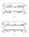
FIG. 4 is a schematic diagram showing a winding state of the wires W1 and W2 in the common mode filter 10. Among constituent elements shown in FIG. 4, an area covering the wires W1 and W2 and the winding core portion 11 a is shown as a cross-sectional view taken along the line A-A shown in FIGS. 2B and 2D. An area covering the flange portions 11 b and 11 c is shown as a top view shown also in FIG. 2A.
The number shown within each of the wires W1 and W2 in FIG. 4 is an illustration of the order of the turn (the turn number of each of the pair-wires) when the number of pair-wires is counted from the end on the side of the flange portion 11 b. In the example in FIG. 4, the maximum value of the turn number is 11. However, the actual number of turns is approximately 40. In FIG. 4, because priority is given to ease of viewing the drawing, a significantly-reduced number of windings of the wires W1 and W2 are shown in a closely-wound portion (described later). In FIG. 4, the connection relationship between the wires W1 and W2 and the terminal electrodes E1 to E4 is schematically shown by thick straight lines. These points are also applied to the drawings explained later.
As shown in FIG. 4, the wires W1 and W2 according to the first embodiment include a first sparsely-wound portion S1 in which the wires W1 and W2 are wound with adjacent pair-wires spaced from each other, and first and second closely-wound portions D1 and D2 in which the wires W1 and W2 are wound with adjacent pair-wires in close contact with each other. The first closely-wound portion D1, the first sparsely-wound portion S1, and the second closely-wound portion D2 are arranged in this order from the flange portion 11 b to the flange portion 11 c. The wires W1 and W2 with the turn numbers 1 to 5 are included in the first closely-wound portion D1. The wires W1 and W2 with the turn number 6 are included in the first sparsely-wound portion S1. The wires W1 and W2 with the turn numbers 7 to 11 are included in the second closely-wound portion D2.
In the first embodiment, one turn (the turn number 6) of each of the wires W1 and W2 is included in the first sparsely-wound portion S1. However, a turn of each of the wires W1 and W2 is not necessarily included in the first sparsely-wound portion S1. This point is also applied to other embodiments described later.
By providing the first sparsely-wound portion S1 as described above, it is possible for the common mode filter 10 according to the first embodiment to reduce the capacitance between different turns in the wires W1 and W2 as compared to the case where no sparsely-wound portion is provided. Therefore, the mode conversion characteristics are also reduced. Meanwhile, because the first and second closely-wound portions D1 and D2 are provided, it is possible for the common mode filter 10 according to the first embodiment to obtain a higher inductance as compared to the case where a space is provided between each of adjacent pair-wires.
FIGS. 5A and 5B are explanatory diagrams of a winding method of the wires W1 and W2 shown in FIG. 4. Each of a straight line and a broken line shown in FIGS. 5A and 5B connects between cross sections of a wire. The straight line schematically shows the wire located on the front side of the winding core portion 11 a in the drawings. The broken line schematically shows the wire located on the rear side of the winding core portion 11 a in the drawings. The method of winding the wires W1 and W2 that include the first and second closely-wound portions D1 and D2, and the first sparsely-wound portion S1 is briefly explained below with reference to FIGS. 5A and 5B.
The wires W1 and W2 are wound around the winding core portion 11 a using an automatic coil winder (not shown). Specifically, as this automatic coil winder, it is preferable to use an automatic coil winder disclosed in Japanese Patent No. 4737268, for example. Assuming that the automatic coil winder disclosed in Japanese Patent No. 4737268 is used, in winding the wires W1 and W2, first, one end of the wire W2 wound as a first layer is joined to the terminal electrode E2, and then while the drum core 11 is rotated about a rotation axis along the y direction at a constant speed, a nozzle that feeds the wire W2 is moved in the y direction (FIG. 5A). At this time, in an area covering the first and second closely-wound portions D1 and D2, the moving speed of the nozzle is adjusted so as not to create a gap between adjacent pair-wires. In contrast, in an area covering the first sparsely-wound portion S1, the moving speed of the nozzle is adjusted so as to create a space of appropriate size between adjacent pair-wires. The moving speed becomes slowest when the wire W2 is wound so as not to create a gap, and becomes faster as a larger space is formed. It is necessary to keep the moving speed of the nozzle constant in the first and second closely-wound portions D1 and D2. However, the moving speed of the nozzle is not necessarily kept constant in the first sparsely-wound portion S1. When winding of the wire W2 is finished, the drum core 11 is stopped rotating, and the other end of the wire W2 is joined to the terminal electrode E4.
Next, one end of the wire W1 wound as a second layer is joined to the terminal electrode E1, and then while the drum core 11 is rotated again at a constant speed, a nozzle that feeds the wire W1 is moved in the y direction (FIG. 5B). At this time, in an area covering the first and second closely-wound portions D1 and D2, the moving speed of the nozzle is adjusted so as to precisely fit the wire W1 between the wires W2. However, because the number of windings of the wire W1 and the number of windings of the wire W2 are the same with each other in either of the first and second closely-wound portions D1 and D2, at one of the ends of each of the first and second closely-wound portions D1 and D2, the wire W1 falls to the first layer as shown in FIG. 5B. In FIG. 5B, the wire W1 with the turn number 1, positioned at the end of the first closely-wound portion D1 on the side of the flange portion 11 b, falls to the first layer, and the wire W1 with the turn number 7, positioned at the end of the second closely-wound portion D2 on the side of the flange portion 11 b, falls to the first layer. Meanwhile, in an area covering the first sparsely-wound portion S1, the moving speed of the nozzle is adjusted so as to wind the wire W1 along the wire W2. That is, within the first sparsely-wound portion S1, the positional relationship between the wires W1 and W2 is the same as in the case of bifilar winding. When winding of the wire W1 is finished, the drum core 11 is stopped rotating, and the other end of the wire W1 is joined to the terminal electrode E3. Following the procedure described above, winding of the wires W1 and W2 around the winding core portion 11 a is completed.
Returning to FIG. 4, the wires W1 and W2 are wound in order that the relationship between the number of turns counted from the flange portion 11 b and the arrangement of a sparsely-wound portion S1, and the relationship between the number of turns counted from the flange portion 11 c and the arrangement of a sparsely-wound portion S1 are the same with each other. In other words, the wires W1 and W2 are wound in order that the wires W1 and W2 wound on the side of the flange portion 11 b and the wires W1 and W2 wound on the side of the flange portion 11 c are symmetric with respect to the center of the winding core portion 11 a in the y-direction. Specifically, according to the number of turns counted from the flange portion 11 b, the first sparsely-wound portion S1 is arranged between the fifth turn and the seventh turn. And, according to the number of turns counted from the flange portion 11 c, the first sparsely-wound portion S1 is also arranged between the fifth turn and the seventh turn.
By setting the relationship between the number of turns and the arrangement of the first sparsely-wound portion S1 as described above, the common mode filter 10 can be expected to exhibit almost the same characteristics both in the case where the terminal electrodes E1 and E2 are utilized as an input terminal and in the case where the terminal electrodes E3 and E4 are utilized as an input terminal. Therefore, at the time of installing the common mode filter 10 on a substrate, it is not necessary to care which of the flange portions corresponds to the terminal electrodes E1 and E2 (the mounting directionality is reduced), and accordingly it is possible to reduce the burden of installation work, and to prevent mistakes with the installation.
The relationship between the number of turns counted from the flange portion 11 b and the arrangement of a sparsely-wound portion S1, and the relationship between the number of turns counted from the flange portion 11 c and the arrangement of a sparsely-wound portion S1 are not necessarily completely the same with each other. It suffices that these relationships are substantially the same with each other. “Substantially the same with each other” means that a difference between those relationships is allowable, from the realistic viewpoint, as long as the mounting directionality is sufficiently reduced. For example, in the case where the total number of turns is 40, when one of the 40 turns is arranged within the first sparsely-wound portion S1 as shown in FIG. 4, then it is inevitable to arrange 19 turns within one of the first and second closely-wound portions D1 and D2, and to arrange 20 turns within the other. In this case, the wires W1 and W2 are not wound in order that the relationship between the number of turns counted from the flange portion 11 b and the arrangement of a sparsely-wound portion S1, and the relationship between the number of turns counted from the flange portion 11 c and the arrangement of a sparsely-wound portion S1 are completely the same with each other. However, from the realistic viewpoint, the mounting directionality is sufficiently reduced. Therefore, in this case, the wires W1 and W2 are thought to be wound in order that the relationship between the number of turns counted from the flange portion 11 b and the arrangement of a sparsely-wound portion S1, and the relationship between the number of turns counted from the flange portion 11 c and the arrangement of a sparsely-wound portion S1 are substantially the same with each other. These points described above are also applied to other embodiments described later and to “the relationship between the number of turns counted from each of the flange portions 11 b and 11 c and the falling position”.
As explained above, in the common mode filter 10 according to the first embodiment, the first sparsely-wound portion S1 is provided, and also the first and second closely-wound portions D1 and D2 are provided. Therefore, both reducing the mode conversion characteristics and ensuring a high impedance can be achieved. Further, because the mounting directionality of the common mode filter 10 can be reduced, it is possible to reduce the operation burden of installing the common mode filter 10 on a substrate, and to prevent mistakes with the installation. Furthermore, because layer winding is employed, it is possible to increase the number of windings as compared to the case where bifilar winding is employed.
FIG. 6 is a schematic diagram showing a modification of the winding state of the wires W1 and W2 shown in FIG. 4. In the modification shown in FIG. 6, in the second closely-wound portion D2, the wires W1 and W2 are wound in order that the wire W1 with the turn number 7, positioned at the end on the side of the flange portion 11 b, does not fall to the first layer, but the wire W1 with the turn number 11, positioned at the end on the side of the flange portion 11 c, falls to the first layer. With this configuration, the relationship between the number of turns counted from the flange portion 11 b and the falling position, and the relationship between the number of turns counted from the flange portion 11 c and the falling position are the same with each other. Therefore, it is possible to further reduce the directionality of the common mode filter 10.
FIG. 7 is a schematic diagram showing a winding state of the wires W1 and W2 in the common mode filter 10 according to a second embodiment of the present invention. The common mode filter 10 according to the second embodiment is the same as the common mode filter 10 according to the first embodiment, except for a winding mode of the wires W1 and W2. In FIG. 7, similarly to FIG. 4, an area covering the wires W1 and W2 and the winding core portion 11 a is shown as a cross-sectional view taken along the line A-A shown in FIGS. 2B and 2D, and an area covering the flange portions 11 b and 11 c is shown as a top view corresponding to FIG. 2A. FIG. 7 is explained below while focusing on the differences from FIG. 4.
As shown in FIG. 7, the wires W1 and W2 according to the second embodiment include first and second sparsely-wound portions S1 and S2 in which the wires W1 and W2 are wound with adjacent pair-wires spaced from each other, and first to third closely-wound portions D1 to D3 in which the wires W1 and W2 are wound with adjacent pair-wires in close contact with each other. The second closely-wound portion D2, the first sparsely-wound portion S1, the first closely-wound portion D1, the second sparsely-wound portion S2, and the third closely-wound portion D3 are arranged in this order from the flange portion 11 b to the flange portion 11 c. The wires W1 and W2 with the turn numbers 1 to 3 are included in the second closely-wound portion D2. The wires W1 and W2 with the turn number 4 are included in the first sparsely-wound portion S1. The wires W1 and W2 with the turn numbers 5 to 7 are included in the first closely-wound portion D1. The wires W1 and W2 with the turn number 8 are included in the second sparsely-wound portion S2. The wires W1 and W2 with the turn numbers 9 to 11 are included in the third closely-wound port ion D3. The second and third closely-wound portions D2 and D3 are not necessarily provided, and can be replaced with one turn of each of the wires W1 and W2.
By providing the first and second sparsely-wound portions S1 and S2 as described above, it is also possible for the common mode filter 10 according to the second embodiment to reduce the capacitance between different turns in the wires W1 and W2 as compared to the case where no sparsely-wound portion is provided. Therefore, the mode conversion characteristics are also reduced. Further, because the first to third closely-wound portions D1 to D3 are provided, it is possible to obtain a higher inductance as compared to the case where a space is provided between each of adjacent pair-wires.
Also in the second embodiment, the wires W1 and W2 are wound in order that the relationship between the number of turns counted from the flange portion 11 b and the arrangement of sparsely-wound portions, and the relationship between the number of turns counted from the flange portion 11 c and the arrangement of sparsely-wound portions are the same with each other. Specifically, according to either the number of turns counted from the flange portion 11 b or the number of turns counted from the flange portion 11 c, the sparsely-wound portions are arranged between the third turn and the fifth turn, and between the seventh turn and the ninth turn. Therefore, similarly to the first embodiment, the mounting directionality can be reduced, and it is possible to reduce the burden of installation work, and to prevent mistakes with the installation.
As explained above, the common mode filter 10 according to the second embodiment can also achieve both reducing the mode conversion characteristics and ensuring a high impedance. Further, because the mounting directionality of the common mode filter 10 can be reduced, it is possible to reduce the operation burden of installing the common mode filter 10 on a substrate, and to prevent mistakes with the installation. Furthermore, because layer winding is employed, it is possible to increase the number of windings as compared to the case where bifilar winding is employed.
In the second embodiment, spaces are formed nearer to the flange portions 11 b and 11 c as compared to the first embodiment. As the positions of the spaces are closer to the flange portions 11 b and 11 c, a larger effect of reducing the mode conversion characteristics can be obtained. Therefore, in the common mode filter 10 according to the second embodiment, it is possible to obtain the effect of reducing the mode conversion characteristics more efficiently (with a narrower space) as compared to the first embodiment.
FIG. 8 is a schematic diagram showing a modification of the winding state of the wires W1 and W2 shown in FIG. 7. In the example in FIG. 7, the wire W1 with the turn numbers 1, 5, and 9, positioned at each end of the first to third closely-wound portions D1 to D3 on the side of the flange portion 11 b, falls to the first layer. However, in the present modification shown in FIG. 8, the wire W1 with the turn numbers 7 and 11, positioned at each end of the first and third closely-wound portions D1 and D3 on the side of the flange portion 11 c, falls to the first layer. With this configuration, the relationship between the number of turns counted from the flange portion 11 b and the falling position, and the relationship between the number of turns counted from the flange portion 11 c and the falling position are not exactly the same with each other, but are similar to each other (substantially the same with each other). Therefore, it is possible to further reduce the directionality of the common mode filter 10 as compared to the example in FIG. 7.
FIG. 9 is a schematic diagram showing a winding state of the wires W1 and W2 in the common mode filter 10 according to a third embodiment of the present invention. The common mode filter 10 according to the third embodiment is the same as the common mode filter 10 according to the first embodiment, except for a winding mode of the wires W1 and W2. In FIG. 9, similarly to FIG. 4, an area covering the wires W1 and W2 and the winding core portion 11 a is shown as a cross-sectional view taken along the line A-A shown in FIGS. 2B and 2D, and an area covering the flange portions 11 b and 11 c is shown as a top view corresponding to FIG. 2A. FIG. 9 is explained below while focusing on the differences from FIG. 4.
As shown in FIG. 9, the wires W1 and W2 according to the third embodiment are wound not by layer winding, but by bifilar winding. Meanwhile, similarly to the first embodiment, the wires W1 and W2 according to the third embodiment include the first sparsely-wound portion S1 in which the wires W1 and W2 are wound with adjacent pair-wires spaced from each other, and the first and second closely-wound portions D1 and D2 in which the wires W1 and W2 are wound with adjacent pair-wires in close contact with each other, and the first closely-wound portion D1, the first sparsely-wound portion S1, and the second closely-wound portion D2 are arranged in this order from the flange portion 11 b to the flange portion 11 c. Therefore, similarly to the first embodiment, in the common mode filter 10 according to the third embodiment, the capacitance between different turns in the wires W1 and W2 is reduced as compared to the case where no sparsely-wound portion is provided, and the mode conversion characteristics are also reduced. Further, it is possible to obtain a higher inductance as compared to the case where a space is provided between each of adjacent pair-wires.
FIG. 10 is an explanatory diagram of a winding method of the wires W1 and W2 shown in FIG. 9. In FIG. 10, similarly to FIGS. 5A and 5B, each of a straight line and a broken line connects between cross sections of a wire. The straight line schematically shows the wire located on the front side of the winding core portion 11 a in the drawing. The broken line schematically shows the wire located on the rear side of the winding core portion 11 a in the drawing. The method of winding the wires W1 and W2 that include the first and second closely-wound portions D1 and D2, and the first sparsely-wound portion S1 by bifilar winding is briefly explained below with reference to FIG. 10.
Similarly to the first embodiment, it is preferable to use the automatic coil winder disclosed in Japanese Patent No. 4737268 as an automatic coil winder used for winding the wires W1 and W2. In the third embodiment, first, one end of the wire W1 is joined to the terminal electrode E1, and one end of the wire W2 is joined to the terminal electrode E2. Next, while the drum core 11 is rotated at a constant speed, two nozzles that feed the wires W1 and W2 respectively are moved in the y direction with their relative positional relationship maintained. At this time, in an area covering the first and second closely-wound portions D1 and D2, the moving speed of each of the nozzles is adjusted so as not to create a gap between adjacent pair-wires. In contrast, in an area covering the first sparsely-wound portion S1, the moving speed of each of the nozzles is adjusted so as to provide a space of appropriate size between adjacent pair-wires. Also in the third embodiment, the moving speed becomes slowest when the wires W1 and W2 are wound so as not to create a gap, and becomes faster as a larger space is formed. Further, it is necessary to keep the moving speed of each of the nozzles constant in the first and second closely-wound portions D1 and D2. However, the moving speed of each of the nozzles is not necessarily kept constant in the first sparsely-wound portion S1. When winding of the wires W1 and W2 is finished, the other end of the wire W1 is joined to the terminal electrode E3, and the other end of the wire W2 is joined to the terminal electrode E4.
Returning to FIG. 9, the wires W1 and W2 are wound in order that the relationship between the number of turns counted from the flange portion 11 b and the arrangement of a sparsely-wound portion S1, and the relationship between the number of turns counted from the flange portion 11 c and the arrangement of a sparsely-wound portion S1 are the same with each other. Specifically, according to either the number of turns counted from the flange portion 11 b or the number of turns counted from the flange portion 11 c, the first sparsely-wound portion S1 is arranged between the third turn and the fifth turn. Therefore, similarly to the first and second embodiments, the mounting directionality can be reduced, and it is possible to reduce the burden of installation work, and to prevent mistakes with the installation.
As explained above, the common mode filter 10 according to the third embodiment can also achieve both reducing the mode conversion characteristics and ensuring a high impedance. Further, because the mounting directionality of the common mode filter 10 can be reduced, it is possible to reduce the operation burden of installing the common mode filter 10 on a substrate, and to prevent mistakes with the installation.
FIG. 11 is a schematic diagram showing a modification of the winding state of the wires W1 and W2 shown in FIG. 9. In FIG. 11, similarly to FIG. 10, each of a straight line and a broken line connects between cross sections of a wire. The straight line schematically shows the wire located on the front side of the winding core portion 11 a in the drawing. The broken line schematically shows the wire located on the rear side of the winding core portion 11 a in the drawing. In the present modification, the wires W1 and W2 cross each other (their positions are interchanged) within the first sparsely-wound portion S1 (at a position X1 shown in FIG. 11). Accordingly, the wires W1 and W2 cross each other also at the end of the second closely-wound portion D2 on the side of the flange portion 11 c (at a position X2 shown in FIG. 11). The crossing of the wires W1 and W2 is realized by interchanging the positions of two nozzles at a corresponding position.
When the wires W1 and W2 cross each other as described above, the polarities are opposite to each other on both sides of the first sparsely-wound portion S1. Therefore, it is possible to balance the polarities. Further, the wires W1 and W2 cross each other within the first sparsely-wound portion S1 (the wires W1 and W2 with the turn number 4, which is not in close contact with its adjacent pair-wires on both sides, cross each other). Therefore, it is possible to minimize winding disarray caused by the crossing of the wires W1 and W2.
FIG. 12 is a schematic diagram showing a winding state of the wires W1 and W2 in the common mode filter 10 according to a fourth embodiment of the present invention. The common mode filter 10 according to the fourth embodiment is the same as the common mode filter 10 according to the third embodiment, except for a winding mode of the wires W1 and W2. In FIG. 12, similarly to FIG. 4, an area covering the wires W1 and W2 and the winding core portion 11 a is shown as a cross-sectional view taken along the line A-A shown in FIGS. 2B and 2D, and an area covering the flange portions 11 b and 11 c is shown as a top view corresponding to FIG. 2A. FIG. 12 is explained below while focusing on the differences from FIG. 4.
Similarly to the third embodiment, the wires W1 and W2 according to the fourth embodiment are wound not by layer winding, but by bifilar winding. Meanwhile, similarly to the second embodiment, the wires W1 and W2 according to the fourth embodiment include the first and second sparsely-wound portions S1 and S2 in which the wires W1 and W2 are wound with adjacent pair-wires spaced from each other, and the first to third closely-wound portions D1 to D3 in which the wires W1 and W2 are wound with adjacent pair-wires in close contact with each other, and the second closely-wound portion D2, the first sparsely-wound portion S1, the first closely-wound portion D1, the second sparsely-wound portion S2, and the third closely-wound portion D3 are arranged in this order from the flange portion 11 b to the flange portion 11 c. Therefore, similarly to the second embodiment, in the common mode filter according to the fourth embodiment, the capacitance between different turns in the wires W1 and W2 is reduced as compared to the case where no sparsely-wound portion is provided, and the mode conversion characteristics are also reduced. Further, it is possible to obtain a higher inductance as compared to the case where a space is provided between each of adjacent pair-wires.
Also in the fourth embodiment, the wires W1 and W2 are wound in order that the relationship between the number of turns counted from the flange portion 11 b and the arrangement of sparsely-wound portions, and the relationship between the number of turns counted from the flange portion 11 c and the arrangement of sparsely-wound portions are the same with each other. Specifically, according to either the number of turns counted from the flange portion 11 b or the number of turns counted from the flange portion 11 c, the sparsely-wound portions are arranged between the second turn and the fourth turn, and between the fifth turn and the seventh turn. Therefore, similarly to the first to third embodiments, the mounting directionality can be reduced, and it is possible to reduce the burden of installation work, and to prevent mistakes with the installation.
As explained above, the common mode filter 10 according to the fourth embodiment can also achieve both reducing the mode conversion characteristics and ensuring a high impedance. Further, because the mounting directionality of the common mode filter 10 can be reduced, it is possible to reduce the operation burden of installing the common mode filter 10 on a substrate, and to prevent mistakes with the installation.
In the fourth embodiment, spaces are formed nearer to the flange portions 11 b and 11 c as compared to the third embodiment. Therefore, it is possible to obtain the effect of reducing the mode conversion characteristics more efficiently (with a narrower space) as compared to the third embodiment.
FIG. 13 is a schematic diagram showing a winding state of the wires W1 and W2 in the common mode filter 10 according to a fifth embodiment of the present invention. The common mode filter 10 according to the fifth embodiment is the same as the common mode filter 10 according to the third and fourth embodiments, except for a winding mode of the wires W1 and W2. In FIG. 13, similarly to FIG. 4, an area covering the wires W1 and W2 and the winding core portion 11 a is shown as a cross-sectional view taken along the line A-A shown in FIGS. 2B and 2D, and an area covering the flange portions 11 b and 11 c is shown as a top view corresponding to FIG. 2A. FIG. 13 is explained below while focusing on the differences from FIG. 4.
As shown in FIG. 13, the wires W1 and W2 according to the fifth embodiment are wound by bifilar winding, and include the first and second sparsely-wound portions S1 and S2 in which the wires W1 and W2 are wound with adjacent pair-wires spaced from each other, and the first closely-wound portion D1 in which the wires W1 and W2 are wound with adjacent pair-wires in close contact with each other. The first sparsely-wound portion S1, the first closely-wound portion D1, and the second sparsely-wound portion S2 are arranged in this order from the flange portion 11 b to the flange portion 11 c. The wires W1 and W2 with the turn numbers 2 and 3 are included in the first sparsely-wound portion S1. The wires W1 and W2 with the turn numbers 10 and 11 are included in the second sparsely-wound portion S2.
Also in the fifth embodiment, the wires W1 and W2 are wound in order that the relationship between the number of turns counted from the flange portion 11 b and the arrangement of sparsely-wound portions, and the relationship between the number of turns counted from the flange portion 11 c and the arrangement of sparsely-wound portions are the same with each other. Specifically, according to either the number of turns counted from the flange portion 11 b or the number of turns counted from the flange portion 11 c, the sparsely-wound portions are arranged between the first turn and the fourth turn, and between the ninth turn and the twelfth turn.
In the common mode filter 10 according to the fifth embodiment, the first and second sparsely-wound portions S1 and S2, and the first closely-wound portion D1 are provided, and therefore the capacitance between different turns in the wires W1 and W2 is reduced as compared to the case where no sparsely-wound portion is provided, and the mode conversion characteristics are also reduced, similarly to the first to fourth embodiments. Further, it is possible to obtain a higher inductance as compared to the case where a space is provided between each of adjacent pair-wires. Furthermore, the wires W1 and W2 are wound in order that the relationship between the number of turns counted from the flange portion 11 b and the arrangement of sparsely-wound portions, and the relationship between the number of turns counted from the flange portion 11 c and the arrangement of sparsely-wound portions are the same with each other. Therefore, the mounting directionality can also be reduced.
In the fifth embodiment, the arrangement of the wires W1 and W2 (with the turn numbers 2 and 3) within the first sparsely-wound portion S1 is set in order that there are distances L1, L2, and L3 between adjacent pair-wires in order from the position closest to the flange portion 11 b, as shown in FIG. 13. Similarly, the arrangement of the wires W1 and W2 (with the turn numbers 10 and 11) within the second sparsely-wound portion S2 is set in order that there are distances L1, L2, and L3 between adjacent pair-wires in order from the position closest to the flange portion 11 c, as shown in FIG. 13.
With this configuration, values of the distances L1 to L3 can be appropriately adjusted. Therefore, in the common mode filter 10 according to the fifth embodiment, it is easier to adjust the mode conversion characteristics to a desired value as compared to the first to fourth embodiments. In view of obtaining the effect of reducing the mode conversion characteristics more efficiently (with a narrower space), it is preferable to select specific values of the distances L1 to L3 so as to satisfy L1>L2>L3 as exemplified in FIG. 13. With this configuration, as spaces are closer to the flange portions 11 b and 11 c, the width of the spaces can be larger, and therefore it is possible to reduce the mode conversion characteristics efficiently.
It is apparent that the present invention is not limited to the above embodiments, but may be modified and changed without departing from the scope and spirit of the invention.
It is possible to apply the configuration as shown in the fifth embodiment for example (FIG. 13), in which the width of plural spaces within a sparsely-wound portion is appropriately adjusted, not only to the bifilar winding shown in FIG. 13, but also to layer winding. For example, also in FIG. 8, two spaces are provided within each of the first and second sparsely-wound portions S1 and S2 (on both sides of the wires W1 and W2 with the turn number 4 and on both sides of the wires W1 and W2 with the turn number 8). The width of these spaces can be appropriately adjusted, thereby adjusting the mode conversion characteristics to a desired value.
In the cross-sectional view of the wires W1 and W2 shown in FIG. 4 and the like, the length of the common mode filter 10 in the y direction is different between the embodiments only for convenience of illustration. The size of the common mode filter 10 is decided according to JIS. At the time of commercialization, the size of the common mode filter 10 is decided from among several standardized sizes (such as 0403, 0605, and 0806). Therefore, it is necessary to select and employ the common mode filter 10 that has characteristics appropriate to its size from the above embodiments. For example, a larger number of windings are obtained by layer winding than by bifilar winding from the same size. Therefore, it suffices that when the size of the common mode filter 10 is small, the layer winding is employed. For another example, when there is room for increasing the size of the common mode filter 10, it suffices that the examples in FIGS. 7 and 12 are employed, in which sparsely-wound portions are provided at a position close to the flange portions 11 b and 11 c. In contrast, when there is no room for increasing the size of the common mode filter 10, it suffices that the examples in FIGS. 4 and 9 are employed, in which one sparsely-wound portion is provided at the center.
Other than that, it is preferable to appropriately select a most appropriate embodiment according to required conditions, such as to employ the example in FIG. 6 in a case where reduction in the directionality is strictly required when the example in FIG. 4 is to be employed, or to employ the example in FIG. 12 in a case where fine adjustments of the mode conversion characteristics are required.

Claims (12)

What is claimed is:
1. A common mode filter, comprising:
a drum core that includes a winding core portion and a pair of flange portions provided at both ends of the winding core portion; and
first and second wires that are wound around the winding core portion so as to form a plurality turns of pair-wire,
the first and second wires including:
one or a plurality of sparsely-wound portions in which adjacent turns of the pair-wire are spaced from each other; and
one or a plurality of closely-wound portions in which adjacent turns of the pair-wire are in close contact with each other,
wherein the one or the plurality of sparsely-wound portions include a first sparsely-wound portion,
wherein the one or the plurality of closely-wound portions include first and second closely-wound portions, and
wherein the first sparsely-wound portion is arranged between the first and second closely-wound portions.
2. The common mode filter as claimed in claim 1, wherein the first and second wires are wound in order that a relationship between a number of each of the pair-wires counted from one of the pair of flange portions and arrangement of the one or plurality of sparsely-wound portions, and a relationship between a number of each of the pair-wires counted from an other flange portion and arrangement of the one or plurality of sparsely-wound portions are substantially the same with each other.
3. The common mode filter as claimed in claim 1, wherein the first and second wires are wound by layer winding in which the second wire is wound as a first layer, and the first wire is wound as a second layer, and
wherein the first and second wires are wound in order that a relationship between a number of each of the pair-wires counted from one of the pair of flange portions and a position at which the first wire falls to the first layer at an end of the first closely-wound portion, and a relationship between a number of each of the pair-wires counted from an other flange portion and a position at which the first wire falls to the first layer at an end of the second closely-wound portion are substantially the same with each other.
4. The common mode filter as claimed in claim 1, wherein the first and second wires are wound by bifilar winding, and
wherein the first and second wires cross each other within the first sparsely-wound portion.
5. The common mode filter as claimed in claim 1, wherein the first and second wires are wound by layer winding.
6. The common mode filter as claimed in claim 1, wherein the first and second wires are wound by bifilar winding.
7. A common mode filter, comprising:
a drum core that includes a winding core portion and a pair of flange portions provided at both ends of the winding core portion; and
first and second wires that are wound around the winding core portion so as to form a plurality turns of pair-wire,
the first and second wires including:
one or a plurality of sparsely-wound portions in which adjacent turns of the pair-wire are spaced from each other; and
one or a plurality of closely-wound portions in which adjacent turns of the pair-wire are in close contact with each other,
wherein the first and second wires are wound in order that a relationship between a number of each of the pair-wires counted from one of the pair of flange portions and arrangement of the one or plurality of sparsely-wound portions, and a relationship between a number of each of the pair-wires counted from an other flange portion and arrangement of the one or plurality of sparsely-wound portions are substantially the same with each other,
wherein the one or the plurality of sparsely-wound portions include a first sparsely-wound portion,
wherein the one or the plurality of closely-wound portions include first and second closely-wound portions, and
wherein the first sparsely-wound portion is arranged between the first and second closely-wound portions,
wherein the first and second wires are wound by bifilar winding, and
wherein the first and second wires cross each other within the first sparsely-wound portion.
8. A common mode filter, comprising:
a winding core portion; and
a pair of wires including first and second wires that are wound around the winding core portion, wherein the pair of wires is wound around the winding core portion in N turns including i−2th turn, i−1th turn, ith turn, i+1th turn, and i+2th turn where i is more than two and less than N−1,
wherein the i−1th turn and the ith turn are wound so as to be spaced from each other,
wherein the ith turn and the i+1th turn are wound so as to be spaced from each other,
wherein the i−1th turn and the i−2th turn are wound so as to be in close contact with each other, and
wherein the i+1th turn and the i+2th turn are wound so as to be in close contact with each other.
9. The common mode filter as claimed in claim 8, wherein the i is (N+1)/2 if the N is an odd number, and the i is N/2 or (N/2)−1 if the N is an even number.
10. The common mode filter as claimed in claim 8, wherein the first and second wires are wound by bifilar winding.
11. The common mode filter as claimed in claim 10, wherein the first and second wires cross each other within an area from the i−1th turn to the i+1th turn.
12. A common mode filter, comprising;
a winding core portion; and
first and second wires that are wound around the winding core portion, each of the first and second wires including at least ith turn, i+1th turn, and i+2th turn,
wherein the ith turn of the first wire and the ith turn of the second wire are wound in a first pitch,
wherein the ith turn of the second wire and the i+1th turn of the first wire are wound in a second pitch,
wherein the i+1th turn of the first wire and the i+1th turn of the second wire are wound in a third pitch,
wherein the i+1th turn of the second wire and the i+2th turn of the first wire are wound in a fourth pitch,
wherein the i+2th turn of the first wire and the i+2th turn of the second wire are wound in a fifth pitch,
wherein the second pitch is wider than each of the first, third, fourth, and fifth pitches,
wherein each of the first and second wires further includes i−1th turn,
wherein the i−1th turn of the first wire and the i−th turn of the second wire are wound in a sixth pitch,
wherein the i−1th turn of the second wire and the ith turn of the first wire are wound in a seventh pitch,
wherein each of the second and seventh pitches is wider than each of the first, third, fourth, fifth, and sixth pitches,
wherein each of the first and second wires further includes i−2th turn,
wherein the i−2th turn of the first wire and the i−2th turn of the second wire are wound in an eighth pitch,
wherein the i−2th turn of the second wire and the i−1th turn of the first wire are wound in a ninth pitch, and
wherein each of the second and seventh pitches is wider than each of the first, third, fourth, fifth, sixth, eighth, and ninth pitches.
US14/045,393 2012-10-05 2013-10-03 Common mode filter Active 2033-11-06 US9362041B2 (en)

Priority Applications (6)

Application Number Priority Date Filing Date Title
US15/142,437 US10037844B2 (en) 2012-10-05 2016-04-29 Common mode filter
US16/011,887 US10522283B2 (en) 2012-10-05 2018-06-19 Common mode filter
US16/690,691 US10755848B2 (en) 2012-10-05 2019-11-21 Common mode filter
US16/928,407 US10910144B2 (en) 2012-10-05 2020-07-14 Common mode filter
US17/141,695 US11545296B2 (en) 2012-10-05 2021-01-05 Common mode filter
US18/072,845 US20230095851A1 (en) 2012-10-05 2022-12-01 Common mode filter

Applications Claiming Priority (2)

Application Number Priority Date Filing Date Title
JP2012-223249 2012-10-05
JP2012223249A JP5821821B2 (en) 2012-10-05 2012-10-05 Common mode filter

Related Child Applications (1)

Application Number Title Priority Date Filing Date
US15/142,437 Continuation US10037844B2 (en) 2012-10-05 2016-04-29 Common mode filter

Publications (2)

Publication Number Publication Date
US20140097928A1 US20140097928A1 (en) 2014-04-10
US9362041B2 true US9362041B2 (en) 2016-06-07

Family

ID=50432247

Family Applications (7)

Application Number Title Priority Date Filing Date
US14/045,393 Active 2033-11-06 US9362041B2 (en) 2012-10-05 2013-10-03 Common mode filter
US15/142,437 Active US10037844B2 (en) 2012-10-05 2016-04-29 Common mode filter
US16/011,887 Active US10522283B2 (en) 2012-10-05 2018-06-19 Common mode filter
US16/690,691 Active US10755848B2 (en) 2012-10-05 2019-11-21 Common mode filter
US16/928,407 Active US10910144B2 (en) 2012-10-05 2020-07-14 Common mode filter
US17/141,695 Active 2034-04-21 US11545296B2 (en) 2012-10-05 2021-01-05 Common mode filter
US18/072,845 Pending US20230095851A1 (en) 2012-10-05 2022-12-01 Common mode filter

Family Applications After (6)

Application Number Title Priority Date Filing Date
US15/142,437 Active US10037844B2 (en) 2012-10-05 2016-04-29 Common mode filter
US16/011,887 Active US10522283B2 (en) 2012-10-05 2018-06-19 Common mode filter
US16/690,691 Active US10755848B2 (en) 2012-10-05 2019-11-21 Common mode filter
US16/928,407 Active US10910144B2 (en) 2012-10-05 2020-07-14 Common mode filter
US17/141,695 Active 2034-04-21 US11545296B2 (en) 2012-10-05 2021-01-05 Common mode filter
US18/072,845 Pending US20230095851A1 (en) 2012-10-05 2022-12-01 Common mode filter

Country Status (2)

Country Link
US (7) US9362041B2 (en)
JP (1) JP5821821B2 (en)

Cited By (4)

* Cited by examiner, † Cited by third party
Publication number Priority date Publication date Assignee Title
US20170288626A1 (en) * 2016-03-30 2017-10-05 Tdk Corporation Common mode filter
CN110098815A (en) * 2018-01-29 2019-08-06 乾坤科技股份有限公司 The common-mode filter of inductive sensor and distribution capacity can be balanced
US20200185145A1 (en) * 2012-12-19 2020-06-11 Tdk Corporation Common mode filter
US20210118607A1 (en) * 2018-06-08 2021-04-22 Murata Manufacturing Co., Ltd. Winding arrangement for use in magnetic devices

Families Citing this family (37)

* Cited by examiner, † Cited by third party
Publication number Priority date Publication date Assignee Title
JP5765400B2 (en) * 2013-03-15 2015-08-19 Tdk株式会社 Common mode filter
JP5971231B2 (en) 2013-12-10 2016-08-17 株式会社村田製作所 Common mode choke coil and manufacturing method thereof
US20150206646A1 (en) * 2013-12-13 2015-07-23 Pulse Electronics, Inc. Methods and apparatus for improving winding balance on inductive devices
JP6205302B2 (en) * 2014-04-15 2017-09-27 株式会社神戸製鋼所 Winding element for noise reduction and inverter device
WO2015178194A1 (en) * 2014-05-19 2015-11-26 株式会社村田製作所 Common-mode choke coil and manufacturing method therefor
JP6578630B2 (en) * 2014-06-19 2019-09-25 Tdk株式会社 Coil component and manufacturing method thereof
JP6287755B2 (en) * 2014-10-23 2018-03-07 株式会社村田製作所 Inductor
JP6589588B2 (en) * 2014-12-02 2019-10-16 Tdk株式会社 Pulse transformer
US9767953B2 (en) * 2014-12-16 2017-09-19 Abc Taiwan Electronics Corp. Common mode filter and core thereof
JP6443104B2 (en) * 2015-02-13 2018-12-26 株式会社村田製作所 Coil parts
US10645811B2 (en) * 2015-07-02 2020-05-05 Pulse Electronics, Inc. Inductive devices with splits and methods of making and using the same
US10003241B2 (en) 2015-07-07 2018-06-19 Kabushiki Kaisha Toyota Jidoshokki Vehicle inverter device and motor-driven compressor
CN107430923B (en) * 2015-10-05 2019-01-18 株式会社村田制作所 Coil component
US10210992B2 (en) 2015-10-06 2019-02-19 Cyntec Co., Ltd. Apparatus of coupled inductors with balanced electromotive forces
JP6443317B2 (en) * 2015-12-15 2018-12-26 株式会社村田製作所 Common mode choke coil
JP6601383B2 (en) * 2016-12-26 2019-11-06 株式会社村田製作所 Inductor parts
JP6794844B2 (en) * 2017-01-23 2020-12-02 Tdk株式会社 Common mode filter
US10878991B2 (en) * 2017-03-22 2020-12-29 Shenzhen Yichong Wireless Power Technology Co. Ltd Sparse-routed magnetic coils for wireless power charging system
JP6955367B2 (en) * 2017-04-28 2021-10-27 太陽誘電株式会社 Manufacturing method of winding type coil parts and winding type coil parts
JP6589934B2 (en) * 2017-05-12 2019-10-16 株式会社村田製作所 Winding device and method of manufacturing coil component
JP7040020B2 (en) * 2018-01-05 2022-03-23 Tdk株式会社 Common mode filter
JP7204468B2 (en) * 2018-01-05 2023-01-16 Tdk株式会社 common mode filter
US11837396B2 (en) 2018-02-05 2023-12-05 Murata Manufacturing Co., Ltd. Common-mode choke coil
JP6879253B2 (en) * 2018-03-30 2021-06-02 株式会社豊田自動織機 In-vehicle electric compressor
TWI650782B (en) * 2018-08-01 2019-02-11 西北臺慶科技股份有限公司 Integrated multi-inductor component
JP6965862B2 (en) * 2018-09-28 2021-11-10 株式会社村田製作所 Coil parts
JP7272789B2 (en) * 2018-12-28 2023-05-12 太陽誘電株式会社 Wound coil parts and drum cores
JP7218589B2 (en) * 2019-01-28 2023-02-07 Tdk株式会社 coil parts
CN109754988B (en) * 2019-02-27 2020-06-23 深圳顺络电子股份有限公司 Coil component and method for manufacturing same
JP7081554B2 (en) * 2019-03-29 2022-06-07 株式会社豊田自動織機 Electric compressor
JP7176466B2 (en) 2019-04-19 2022-11-22 株式会社村田製作所 coil parts
JP7028219B2 (en) 2019-04-19 2022-03-02 株式会社村田製作所 Coil parts and manufacturing method of coil parts
JP7205365B2 (en) 2019-04-19 2023-01-17 株式会社村田製作所 coil parts
JP7270122B2 (en) * 2019-12-25 2023-05-10 パナソニックIpマネジメント株式会社 common mode choke coil
JP7424219B2 (en) * 2020-06-16 2024-01-30 Tdk株式会社 common mode filter
JP2022062301A (en) * 2020-10-08 2022-04-20 株式会社村田製作所 Common mode choke coil
CN114915173A (en) * 2021-02-08 2022-08-16 台达电子工业股份有限公司 Flexible cutting type power converter

Citations (16)

* Cited by examiner, † Cited by third party
Publication number Priority date Publication date Assignee Title
JP2002246244A (en) 2001-02-15 2002-08-30 Murata Mfg Co Ltd Choke coil
JP2003234218A (en) 2002-02-12 2003-08-22 Tdk Corp Common-mode filter and its manufacturing method
JP2004146683A (en) * 2002-10-25 2004-05-20 Tdk Corp Surface-mount common mode noise filter
US20050052267A1 (en) * 2003-07-25 2005-03-10 Kyocera Corporation Ferrite core, method of manufacturing the same, and common-mode noise filter using the same
JP2006049383A (en) 2004-07-30 2006-02-16 Taiyo Yuden Co Ltd Common mode choke coil
US20060170526A1 (en) * 2005-01-31 2006-08-03 Tdk Corporation Coil assembly including common-mode choke coil
JP2007324380A (en) 2006-06-01 2007-12-13 Nec Tokin Corp Common-mode choke coil for high-frequency waves
JP2008034777A (en) 2006-07-31 2008-02-14 Taiyo Yuden Co Ltd Common mode choke coil
US20080309445A1 (en) * 2007-06-14 2008-12-18 Tdk Corporation Transformer
JP2009021558A (en) 2007-06-14 2009-01-29 Tdk Corp Transformer component
JP2009094389A (en) 2007-10-11 2009-04-30 Taiyo Yuden Co Ltd Winding wire type coil component
US20090295525A1 (en) * 2008-05-29 2009-12-03 Tdk Corporation Inductor component
JP2011138914A (en) 2009-12-28 2011-07-14 Tdk Corp Coil component
JP4737268B2 (en) 2008-10-31 2011-07-27 Tdk株式会社 Surface mount pulse transformer and method and apparatus for manufacturing the same
JP4789076B2 (en) 2007-12-14 2011-10-05 Tdk株式会社 Coil parts
JP2011253888A (en) 2010-06-01 2011-12-15 Tdk Corp Coil component and coil component manufacturing method

Family Cites Families (7)

* Cited by examiner, † Cited by third party
Publication number Priority date Publication date Assignee Title
JPS4833347A (en) 1971-09-02 1973-05-09
US5483208A (en) * 1994-08-26 1996-01-09 Scientific-Atlanta, Inc. Radio frequency choke and tap
JP3755488B2 (en) * 2001-08-09 2006-03-15 株式会社村田製作所 Wire wound type chip coil and its characteristic adjusting method
CN101501791A (en) * 2006-07-14 2009-08-05 美商·帕斯脉冲工程有限公司 Self-leaded surface mount inductors and methods
JP2008091359A (en) * 2006-09-29 2008-04-17 Toko Inc Winding type common mode choke coil
CN101449346B (en) * 2007-02-05 2012-07-18 株式会社村田制作所 Winding type coil and its winding method
WO2009028406A1 (en) * 2007-08-31 2009-03-05 Murata Manufacturing Co., Ltd. Wire-wound coil and wire-wound coil manufacturing method

Patent Citations (17)

* Cited by examiner, † Cited by third party
Publication number Priority date Publication date Assignee Title
JP2002246244A (en) 2001-02-15 2002-08-30 Murata Mfg Co Ltd Choke coil
JP2003234218A (en) 2002-02-12 2003-08-22 Tdk Corp Common-mode filter and its manufacturing method
JP2004146683A (en) * 2002-10-25 2004-05-20 Tdk Corp Surface-mount common mode noise filter
JP3973028B2 (en) 2002-10-25 2007-09-05 Tdk株式会社 Surface mount type common mode noise filter
US20050052267A1 (en) * 2003-07-25 2005-03-10 Kyocera Corporation Ferrite core, method of manufacturing the same, and common-mode noise filter using the same
JP2006049383A (en) 2004-07-30 2006-02-16 Taiyo Yuden Co Ltd Common mode choke coil
US20060170526A1 (en) * 2005-01-31 2006-08-03 Tdk Corporation Coil assembly including common-mode choke coil
JP2007324380A (en) 2006-06-01 2007-12-13 Nec Tokin Corp Common-mode choke coil for high-frequency waves
JP2008034777A (en) 2006-07-31 2008-02-14 Taiyo Yuden Co Ltd Common mode choke coil
US20080309445A1 (en) * 2007-06-14 2008-12-18 Tdk Corporation Transformer
JP2009021558A (en) 2007-06-14 2009-01-29 Tdk Corp Transformer component
JP2009094389A (en) 2007-10-11 2009-04-30 Taiyo Yuden Co Ltd Winding wire type coil component
JP4789076B2 (en) 2007-12-14 2011-10-05 Tdk株式会社 Coil parts
US20090295525A1 (en) * 2008-05-29 2009-12-03 Tdk Corporation Inductor component
JP4737268B2 (en) 2008-10-31 2011-07-27 Tdk株式会社 Surface mount pulse transformer and method and apparatus for manufacturing the same
JP2011138914A (en) 2009-12-28 2011-07-14 Tdk Corp Coil component
JP2011253888A (en) 2010-06-01 2011-12-15 Tdk Corp Coil component and coil component manufacturing method

Cited By (8)

* Cited by examiner, † Cited by third party
Publication number Priority date Publication date Assignee Title
US20200185145A1 (en) * 2012-12-19 2020-06-11 Tdk Corporation Common mode filter
US11636973B2 (en) * 2012-12-19 2023-04-25 Tdk Corporation Common mode filter
US20170288626A1 (en) * 2016-03-30 2017-10-05 Tdk Corporation Common mode filter
US10193516B2 (en) * 2016-03-30 2019-01-29 Tdk Corporation Common mode filter
CN110098815A (en) * 2018-01-29 2019-08-06 乾坤科技股份有限公司 The common-mode filter of inductive sensor and distribution capacity can be balanced
TWI682629B (en) * 2018-01-29 2020-01-11 乾坤科技股份有限公司 Common mode filter capable of balancing induced inductance and distributed capacitance
US10559415B2 (en) 2018-01-29 2020-02-11 Cyntec Co., Ltd. Common mode filter capable of balancing induced inductance and distributed capacitance
US20210118607A1 (en) * 2018-06-08 2021-04-22 Murata Manufacturing Co., Ltd. Winding arrangement for use in magnetic devices

Also Published As

Publication number Publication date
US20230095851A1 (en) 2023-03-30
US10522283B2 (en) 2019-12-31
JP5821821B2 (en) 2015-11-24
US20180301275A1 (en) 2018-10-18
US20160247625A1 (en) 2016-08-25
JP2014075533A (en) 2014-04-24
US20200090857A1 (en) 2020-03-19
US10755848B2 (en) 2020-08-25
US20140097928A1 (en) 2014-04-10
US10037844B2 (en) 2018-07-31
US11545296B2 (en) 2023-01-03
US20200343035A1 (en) 2020-10-29
US10910144B2 (en) 2021-02-02
US20210125772A1 (en) 2021-04-29

Similar Documents

Publication Publication Date Title
US10910144B2 (en) Common mode filter
US11636973B2 (en) Common mode filter
US10374568B2 (en) Common mode filter
US9502169B2 (en) Common mode choke coil and manufacturing method thereof
JP6601383B2 (en) Inductor parts
JP6010746B2 (en) Common mode noise filter
JP6202165B2 (en) Common mode filter
US11605485B2 (en) Common mode filter
US10958233B2 (en) Common mode filter
US10778177B2 (en) Common mode noise filter
JP2013062477A (en) Common mode choke coil
JP6336155B2 (en) Common mode filter
JP6563073B2 (en) Common mode filter
JP7067501B2 (en) Coil parts
JP5387502B2 (en) Coil parts and impedance adjustment method
JP5996007B2 (en) Common mode filter
JP6583472B2 (en) Common mode filter
JP6495807B2 (en) Common mode choke coil
JP5996008B2 (en) Common mode filter
JP7270122B2 (en) common mode choke coil
US20230223180A1 (en) Common mode filter

Legal Events

Date Code Title Description
AS Assignment

Owner name: TDK CORPORATION, JAPAN

Free format text: ASSIGNMENT OF ASSIGNORS INTEREST;ASSIGNORS:TOMONARI, TOSHIO;KOBAYASHI, TSUTOMU;ARIMITSU, KAZUNORI;REEL/FRAME:031439/0909

Effective date: 20130924

STCF Information on status: patent grant

Free format text: PATENTED CASE

MAFP Maintenance fee payment

Free format text: PAYMENT OF MAINTENANCE FEE, 4TH YEAR, LARGE ENTITY (ORIGINAL EVENT CODE: M1551); ENTITY STATUS OF PATENT OWNER: LARGE ENTITY

Year of fee payment: 4

MAFP Maintenance fee payment

Free format text: PAYMENT OF MAINTENANCE FEE, 8TH YEAR, LARGE ENTITY (ORIGINAL EVENT CODE: M1552); ENTITY STATUS OF PATENT OWNER: LARGE ENTITY

Year of fee payment: 8