US9353442B2 - Apparatus for forming silicon-containing thin film - Google Patents
Apparatus for forming silicon-containing thin film Download PDFInfo
- Publication number
- US9353442B2 US9353442B2 US14/576,410 US201414576410A US9353442B2 US 9353442 B2 US9353442 B2 US 9353442B2 US 201414576410 A US201414576410 A US 201414576410A US 9353442 B2 US9353442 B2 US 9353442B2
- Authority
- US
- United States
- Prior art keywords
- silicon
- seed layer
- order
- based gas
- forming
- Prior art date
- Legal status (The legal status is an assumption and is not a legal conclusion. Google has not performed a legal analysis and makes no representation as to the accuracy of the status listed.)
- Active, expires
Links
Images


Classifications
-
- C—CHEMISTRY; METALLURGY
- C23—COATING METALLIC MATERIAL; COATING MATERIAL WITH METALLIC MATERIAL; CHEMICAL SURFACE TREATMENT; DIFFUSION TREATMENT OF METALLIC MATERIAL; COATING BY VACUUM EVAPORATION, BY SPUTTERING, BY ION IMPLANTATION OR BY CHEMICAL VAPOUR DEPOSITION, IN GENERAL; INHIBITING CORROSION OF METALLIC MATERIAL OR INCRUSTATION IN GENERAL
- C23C—COATING METALLIC MATERIAL; COATING MATERIAL WITH METALLIC MATERIAL; SURFACE TREATMENT OF METALLIC MATERIAL BY DIFFUSION INTO THE SURFACE, BY CHEMICAL CONVERSION OR SUBSTITUTION; COATING BY VACUUM EVAPORATION, BY SPUTTERING, BY ION IMPLANTATION OR BY CHEMICAL VAPOUR DEPOSITION, IN GENERAL
- C23C16/00—Chemical coating by decomposition of gaseous compounds, without leaving reaction products of surface material in the coating, i.e. chemical vapour deposition [CVD] processes
- C23C16/44—Chemical coating by decomposition of gaseous compounds, without leaving reaction products of surface material in the coating, i.e. chemical vapour deposition [CVD] processes characterised by the method of coating
- C23C16/52—Controlling or regulating the coating process
-
- C—CHEMISTRY; METALLURGY
- C23—COATING METALLIC MATERIAL; COATING MATERIAL WITH METALLIC MATERIAL; CHEMICAL SURFACE TREATMENT; DIFFUSION TREATMENT OF METALLIC MATERIAL; COATING BY VACUUM EVAPORATION, BY SPUTTERING, BY ION IMPLANTATION OR BY CHEMICAL VAPOUR DEPOSITION, IN GENERAL; INHIBITING CORROSION OF METALLIC MATERIAL OR INCRUSTATION IN GENERAL
- C23C—COATING METALLIC MATERIAL; COATING MATERIAL WITH METALLIC MATERIAL; SURFACE TREATMENT OF METALLIC MATERIAL BY DIFFUSION INTO THE SURFACE, BY CHEMICAL CONVERSION OR SUBSTITUTION; COATING BY VACUUM EVAPORATION, BY SPUTTERING, BY ION IMPLANTATION OR BY CHEMICAL VAPOUR DEPOSITION, IN GENERAL
- C23C16/00—Chemical coating by decomposition of gaseous compounds, without leaving reaction products of surface material in the coating, i.e. chemical vapour deposition [CVD] processes
- C23C16/02—Pretreatment of the material to be coated
- C23C16/0272—Deposition of sub-layers, e.g. to promote the adhesion of the main coating
-
- C—CHEMISTRY; METALLURGY
- C23—COATING METALLIC MATERIAL; COATING MATERIAL WITH METALLIC MATERIAL; CHEMICAL SURFACE TREATMENT; DIFFUSION TREATMENT OF METALLIC MATERIAL; COATING BY VACUUM EVAPORATION, BY SPUTTERING, BY ION IMPLANTATION OR BY CHEMICAL VAPOUR DEPOSITION, IN GENERAL; INHIBITING CORROSION OF METALLIC MATERIAL OR INCRUSTATION IN GENERAL
- C23C—COATING METALLIC MATERIAL; COATING MATERIAL WITH METALLIC MATERIAL; SURFACE TREATMENT OF METALLIC MATERIAL BY DIFFUSION INTO THE SURFACE, BY CHEMICAL CONVERSION OR SUBSTITUTION; COATING BY VACUUM EVAPORATION, BY SPUTTERING, BY ION IMPLANTATION OR BY CHEMICAL VAPOUR DEPOSITION, IN GENERAL
- C23C16/00—Chemical coating by decomposition of gaseous compounds, without leaving reaction products of surface material in the coating, i.e. chemical vapour deposition [CVD] processes
- C23C16/22—Chemical coating by decomposition of gaseous compounds, without leaving reaction products of surface material in the coating, i.e. chemical vapour deposition [CVD] processes characterised by the deposition of inorganic material, other than metallic material
- C23C16/24—Deposition of silicon only
-
- C—CHEMISTRY; METALLURGY
- C30—CRYSTAL GROWTH
- C30B—SINGLE-CRYSTAL GROWTH; UNIDIRECTIONAL SOLIDIFICATION OF EUTECTIC MATERIAL OR UNIDIRECTIONAL DEMIXING OF EUTECTOID MATERIAL; REFINING BY ZONE-MELTING OF MATERIAL; PRODUCTION OF A HOMOGENEOUS POLYCRYSTALLINE MATERIAL WITH DEFINED STRUCTURE; SINGLE CRYSTALS OR HOMOGENEOUS POLYCRYSTALLINE MATERIAL WITH DEFINED STRUCTURE; AFTER-TREATMENT OF SINGLE CRYSTALS OR A HOMOGENEOUS POLYCRYSTALLINE MATERIAL WITH DEFINED STRUCTURE; APPARATUS THEREFOR
- C30B25/00—Single-crystal growth by chemical reaction of reactive gases, e.g. chemical vapour-deposition growth
- C30B25/02—Epitaxial-layer growth
- C30B25/18—Epitaxial-layer growth characterised by the substrate
- C30B25/183—Epitaxial-layer growth characterised by the substrate being provided with a buffer layer, e.g. a lattice matching layer
-
- C—CHEMISTRY; METALLURGY
- C30—CRYSTAL GROWTH
- C30B—SINGLE-CRYSTAL GROWTH; UNIDIRECTIONAL SOLIDIFICATION OF EUTECTIC MATERIAL OR UNIDIRECTIONAL DEMIXING OF EUTECTOID MATERIAL; REFINING BY ZONE-MELTING OF MATERIAL; PRODUCTION OF A HOMOGENEOUS POLYCRYSTALLINE MATERIAL WITH DEFINED STRUCTURE; SINGLE CRYSTALS OR HOMOGENEOUS POLYCRYSTALLINE MATERIAL WITH DEFINED STRUCTURE; AFTER-TREATMENT OF SINGLE CRYSTALS OR A HOMOGENEOUS POLYCRYSTALLINE MATERIAL WITH DEFINED STRUCTURE; APPARATUS THEREFOR
- C30B29/00—Single crystals or homogeneous polycrystalline material with defined structure characterised by the material or by their shape
- C30B29/02—Elements
- C30B29/06—Silicon
-
- H—ELECTRICITY
- H01—ELECTRIC ELEMENTS
- H01L—SEMICONDUCTOR DEVICES NOT COVERED BY CLASS H10
- H01L21/00—Processes or apparatus adapted for the manufacture or treatment of semiconductor or solid state devices or of parts thereof
- H01L21/02—Manufacture or treatment of semiconductor devices or of parts thereof
- H01L21/02104—Forming layers
- H01L21/02365—Forming inorganic semiconducting materials on a substrate
- H01L21/02367—Substrates
- H01L21/0237—Materials
- H01L21/02373—Group 14 semiconducting materials
- H01L21/02381—Silicon, silicon germanium, germanium
-
- H—ELECTRICITY
- H01—ELECTRIC ELEMENTS
- H01L—SEMICONDUCTOR DEVICES NOT COVERED BY CLASS H10
- H01L21/00—Processes or apparatus adapted for the manufacture or treatment of semiconductor or solid state devices or of parts thereof
- H01L21/02—Manufacture or treatment of semiconductor devices or of parts thereof
- H01L21/02104—Forming layers
- H01L21/02365—Forming inorganic semiconducting materials on a substrate
- H01L21/02436—Intermediate layers between substrates and deposited layers
- H01L21/02439—Materials
- H01L21/02441—Group 14 semiconducting materials
- H01L21/0245—Silicon, silicon germanium, germanium
-
- H—ELECTRICITY
- H01—ELECTRIC ELEMENTS
- H01L—SEMICONDUCTOR DEVICES NOT COVERED BY CLASS H10
- H01L21/00—Processes or apparatus adapted for the manufacture or treatment of semiconductor or solid state devices or of parts thereof
- H01L21/02—Manufacture or treatment of semiconductor devices or of parts thereof
- H01L21/02104—Forming layers
- H01L21/02365—Forming inorganic semiconducting materials on a substrate
- H01L21/02436—Intermediate layers between substrates and deposited layers
- H01L21/02439—Materials
- H01L21/02488—Insulating materials
-
- H—ELECTRICITY
- H01—ELECTRIC ELEMENTS
- H01L—SEMICONDUCTOR DEVICES NOT COVERED BY CLASS H10
- H01L21/00—Processes or apparatus adapted for the manufacture or treatment of semiconductor or solid state devices or of parts thereof
- H01L21/02—Manufacture or treatment of semiconductor devices or of parts thereof
- H01L21/02104—Forming layers
- H01L21/02365—Forming inorganic semiconducting materials on a substrate
- H01L21/02436—Intermediate layers between substrates and deposited layers
- H01L21/02494—Structure
- H01L21/02496—Layer structure
- H01L21/02505—Layer structure consisting of more than two layers
-
- H—ELECTRICITY
- H01—ELECTRIC ELEMENTS
- H01L—SEMICONDUCTOR DEVICES NOT COVERED BY CLASS H10
- H01L21/00—Processes or apparatus adapted for the manufacture or treatment of semiconductor or solid state devices or of parts thereof
- H01L21/02—Manufacture or treatment of semiconductor devices or of parts thereof
- H01L21/02104—Forming layers
- H01L21/02365—Forming inorganic semiconducting materials on a substrate
- H01L21/02518—Deposited layers
- H01L21/02521—Materials
- H01L21/02524—Group 14 semiconducting materials
- H01L21/02532—Silicon, silicon germanium, germanium
-
- H—ELECTRICITY
- H01—ELECTRIC ELEMENTS
- H01L—SEMICONDUCTOR DEVICES NOT COVERED BY CLASS H10
- H01L21/00—Processes or apparatus adapted for the manufacture or treatment of semiconductor or solid state devices or of parts thereof
- H01L21/02—Manufacture or treatment of semiconductor devices or of parts thereof
- H01L21/02104—Forming layers
- H01L21/02365—Forming inorganic semiconducting materials on a substrate
- H01L21/02518—Deposited layers
- H01L21/0257—Doping during depositing
- H01L21/02573—Conductivity type
-
- H—ELECTRICITY
- H01—ELECTRIC ELEMENTS
- H01L—SEMICONDUCTOR DEVICES NOT COVERED BY CLASS H10
- H01L21/00—Processes or apparatus adapted for the manufacture or treatment of semiconductor or solid state devices or of parts thereof
- H01L21/02—Manufacture or treatment of semiconductor devices or of parts thereof
- H01L21/02104—Forming layers
- H01L21/02365—Forming inorganic semiconducting materials on a substrate
- H01L21/02612—Formation types
- H01L21/02617—Deposition types
- H01L21/0262—Reduction or decomposition of gaseous compounds, e.g. CVD
-
- H10P14/24—
-
- H10P14/2905—
-
- H10P14/3211—
-
- H10P14/3238—
-
- H10P14/3251—
-
- H10P14/3411—
-
- H10P14/3441—
Definitions
- the present invention relates to a method of forming a seed layer, a method of forming a silicon-containing thin film and an apparatus for forming a silicon-containing thin film.
- Patent Reference 1 discloses a film forming method for forming an amorphous silicon film by using a disilane gas.
- One of the indexes for evaluating “quality of a film” is a uniformity of a film thickness within a wafer surface (thickness uniformity).
- Patent Reference 1 when forming an amorphous silicon film, a film forming temperature is set to be 530° C. or lower, and a flow rate of the disilane gas is set as 300 cc or higher per minute. Accordingly, an amorphous silicon film having excellent thickness uniformity is obtained.
- the flow rate of the disilane gas ranges from 1000 cc to 2000 cc, and the film forming temperature ranges from 450° C. to 475° C., and accordingly, the amorphous silicon film having the thickness uniformity of about ⁇ 3.0 to 7.0%, which is very excellent, has been obtained.
- the present invention provides a method of forming a seed layer for forming a thin film, a method of forming a silicon-containing thin film using the seed layer and an apparatus for forming a silicon-containing thin film, which are capable of improving a thickness uniformity of a thin film.
- an apparatus for forming a silicon-containing thin film comprising: a processing chamber in which a substrate having a base is disposed; a process gas supply mechanism which supplies gas used for a process into the processing chamber; a heating device which heats the substrate; an exhauster which evacuates the interior of the processing chamber; and a controller which is configured to control the process gas supplying mechanism, the heating device, and the exhauster to perform: forming a first seed layer on the base by adsorbing at least silicon included in an aminosilane-based gas on the base, using the aminosilane-based gas; forming a second seed layer on the first seed layer by depositing at least silicon included in a higher-order silane-based gas having an order that is equal to or higher than disilane, using the higher-order silane-based gas having an order that is equal to or higher than the disilane, wherein the first seed layer and the second seed layer form a dual seed layer; and forming the silicon-containing thin film
- an apparatus for forming a silicon-containing thin film comprising: a processing chamber in which a substrate having a base is disposed; a process gas supply mechanism which supplies gas used for a process into the processing chamber; a heating device which heats the substrate; an exhauster which evacuates the interior of the processing chamber; and a controller which is configured to control the process gas supplying mechanism, the heating device, and the exhauster to perform: forming a mixed seed layer on the base, using both of an aminosilane-based gas and a higher-order silane-based gas having an order that is equal to or higher than the disilane, by adsorbing at least silicon included in the aminosilane-based gas on the base, filling sites, where at least the silicon included in the aminosilane-based gas is not adsorbed, with at least silicon included in the higher-order silane-based gas having an order that is equal to or higher than disilane, and depositing at least the silicon included in the higher-order si
- FIG. 1 is a flowchart describing an example of a method of forming a seed layer and a method of forming a silicon-containing thin film, according to an embodiment of the present invention
- FIGS. 2A through 2C are cross-sectional views showing principal processes of the method of forming a seed layer and the method of forming a silicon-containing thin film, according to the first embodiment of the present invention
- FIG. 3 is a graph showing film thickness versus thickness uniformity
- FIG. 4 is a flowchart describing a method of forming a seed layer and a method of forming a silicon-containing thin film, according to a second embodiment of the present invention
- FIGS. 5A through 5C are cross-sectional views showing principal processes of the method of forming a seed layer and the method of forming a silicon-containing thin film, according to the second embodiment of the present invention.
- FIG. 6 is a flowchart describing a method of forming a seed layer and a method of forming a silicon-containing thin film, according to a third embodiment of the present invention.
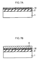
- FIGS. 7A and 7B are cross-sectional views showing principal processes of the method of forming a seed layer and the method of forming a silicon-containing thin film, according to the third embodiment of the present invention.
- FIG. 8 is a sectional view schematically showing an example of a film formation apparatus capable of implementing a silicon-containing thin film formation method according to the fourth embodiment of the present invention.
- FIG. 1 is a flowchart describing an example of a method of forming a seed layer and a method of forming a silicon-containing thin film, according to a first embodiment of the present invention
- FIGS. 2A through 2C are cross-sectional views showing principal processes of the method of forming a seed layer and the method of forming a silicon-containing thin film according to the first embodiment.
- SiO 2 silicon oxide
- An example of the method of forming a seed layer according to the first embodiment is as follows.
- step 11 of FIG. 1 and in FIG. 2A by using an aminosilane-based gas, at least silicon* 1 included in the aminosilane-based gas is adsorbed to a silicon oxide film 2 formed on a silicon substrate 1 .
- the silicon substrate 1 is heated, and the aminosilane-based gas flows onto a main surface of the silicon oxide film 2 as a raw material gas for forming a first seed layer.
- a component including at least silicon, which is included in the aminosilane-based gas is adsorbed to the main surface of the silicon oxide film 2 , and a first seed layer 3 adsorbed at an atomic layer level, for example, a layer level of atoms (monatomic layer order), is formed.
- the first seed layer 3 is a very thin layer.
- FIG. 2A shows the first seed layer 3 , in which silicon atoms are adsorbed as grains.
- the first seed layer 3 may be formed by, for example, an atomic layer deposition (ALD) method, in which a material of a thin film is stacked by a monatomic layer order.
- ALD atomic layer deposition
- aminosilane-based gas may be a gas including at least one of:
- BTBAS Bis(tertiary-butylamino)silane
- TDMAS tris(dimethylamino)silane
- DIPAS diisopropyl aminosilane
- DIPAS is used.
- Processing temperature 400° C.
- step 12 of FIG. 1 and FIG. 2B by using a silane-based gas having an order higher than disilane, at least silicon included in the higher-order silane-based gas having an order equal to or higher than disilane is deposited on the silicon oxide film 2 , on which the at least silicon* 1 included in the aminosilane-based gas is adsorbed, that is, the first seed layer 3 is formed.
- the silicon substrate 1 is heated, and the higher-order silane-based gas, that is, having an order that is equal to or higher than disilane, is flown on the main surface of the silicon substrate 1 , on which the first seed layer 3 is formed, as a raw material gas for forming a second seed layer.
- the second seed layer 4 may be formed on the first seed layer 3 while, for example, filling between grains of the first seed layer 3 , in a case where the first seed layer 3 is configured to include the grains.
- the second seed layer 4 may be formed by using, for example, a chemical vapor deposition (CVD) method, in which a raw material of the thin film is deposited by a CVD reaction.
- CVD chemical vapor deposition
- An example of the higher-order silane-based gas having an order that is equal to or higher than disilane may include at least one of:
- a silicon hydride expressed as Si m H 2m+2 , where m is a natural number that is greater than or equal to 3, and
- n H 2n a silicon hydride expressed as Si n H 2n , where n is a natural number that is greater than or equal to 3.
- the silicon hydride expressed as Si m H 2m+2 is selected from at least one of:
- the silicon hydride expressed as Si n H 2n , where n is a natural number that is greater than or equal to 3, is selected from at least one of:
- disilane is used as the higher-order silane-based gas having an order that is equal to or higher than disilane.
- Examples of processing conditions when forming the second seed layer 4 are:
- Processing temperature 400° C.
- a dual seed layer 5 including the first seed layer 3 and the second seed layer 4 formed on the first seed layer 3 , is formed.
- the dual seed layer 5 is in, for example, an amorphous state.
- a thickness of the dual seed layer 5 may be, for example, greater than 0 nm and equal to or less than 2 nm, in consideration of a film thickness including the thickness of the dual seed layer 5 and a thickness of the main film of the thin film.
- the second seed layer 4 in the dual seed layer 5 may be doped with a dopant.
- a gas containing the dopant may be supplied with the higher-order silane-based gas having an order that is equal to or higher than disilane.
- Examples of the dopant may be:
- the above dopants may be mixed. That is, the gas including at least one dopant selected from the above six kinds of dopants may be supplied with the higher-order silane-based gas having an order that is equal to or higher than disilane to form the second seed layer 4 .
- the silicon included in the higher-order silane-based gas having an order that is equal to or higher than disilane is deposited on the silicon substrate 1 , on which at least the silicon included in the aminosilane-based gas is adsorbed, wherein the silicon included in the higher-order silane-based gas having an order that is equal to or higher than disilane contains at least one of the above six kinds of dopants.
- a silicon-containing thin film 6 is formed on the silicon substrate 1 , on which the dual seed layer 5 is formed, as the main film of the thin film.
- silicon-containing thin film 6 may be a silicon (Si) film or a silicon germanium (SiGe) film.
- the silicon-containing thin film 6 may be formed as follows.
- a lower-order silane-based gas having an order that is lower than the above higher-order silane-based gas having an order that is equal to or higher than disilane is used as a raw material gas for forming the silicon film.
- a disilane gas is used to form the second seed layer 4
- a monosilane gas may be used as the raw material gas for forming the silicon film.
- Examples of processing conditions when the silicon-containing thin film 6 is the silicon film and the monosilane gas is used as the raw material gas are:
- Processing pressure 53.3 Pa (0.4 Torr). Under the above processing conditions, a silicon film having a thickness of about 3 nm is formed as the main film of the thin film.
- a lower-order silane-based gas having an order that is lower than the higher-order silane-based gas having an order that is equal to or higher than disilane and a monogermane (GeH 4 ) gas are used as a raw material gas of the silicon germanium film.
- a monosilane gas and the monogermane gas may be used as the raw material gas of the silicon germanium film.
- Examples of processing conditions when the silicon-containing thin film 6 is the silicon germanium film and the monosilane gas and the monogermane gas are used as the raw material gas are:
- Processing temperature 400° C.
- Processing pressure 533 Pa (4 Torr). Under the above processing conditions, a silicon germanium film having a thickness of about 4 nm is formed as the main film of the thin film.
- the silicon-containing thin film 6 which is composed of the silicon film or the silicon germanium film is formed on the dual seed layer 5 .
- the silicon-containing thin film 6 may be in one of:
- the state of the silicon-containing thin film 6 after the film formation may be determined during the forming of the silicon-containing thin film 6 , or according to a process after the formation of the silicon-containing thin film 6 . For example, if the state is determined during the formation of the silicon-containing thin film 6 , the processing temperature, the processing pressure, and the flow of the raw material gas may be adjusted. In addition, if the state is determined after the formation of the silicon-containing thin film 6 , the silicon substrate 1 on which the silicon-containing thin film 6 is formed may be annealed. The state of the silicon-containing thin film 6 may be controlled to one of the above four states by adjusting a processing temperature, a processing pressure, and a processing time of the annealing.
- the silicon-containing thin film 6 is a main film of the thin film.
- the thickness of the thin film to be formed is almost dependent upon the thickness of the silicon-containing thin film 6 .
- the thickness of the silicon-containing thin film 6 is determined according to demands of a user. However, in consideration of practical use, the thickness of the silicon-containing thin film 6 may be greater than 0 nm and equal to or less than 100 nm.
- the silicon-containing thin film 6 may be doped with a dopant.
- Examples of the dopant may be:
- the above dopants may be mixed, like the dopant with which the second seed layer 4 is doped.
- the dopant may be doped during the formation of the silicon-containing thin film 6 or after the formation of the silicon-containing thin film 6 . If the dopant is doped during the formation of the silicon-containing thin film 6 , in the process shown in step 1 of FIG. 1 and FIG. 2C , a gas containing the dopant may be supplied with, for example, the raw material gas. If the dopant is doped after the formation of the silicon-containing thin film 6 , the dopant may be diffused in the silicon-containing thin film 6 through a vapor deposition process.
- FIG. 3 is a graph showing a relationship between film thickness and thickness uniformity.
- FIG. 3 shows a relationship between the film thickness and the thickness uniformity of the silicon-containing thin film 6 formed on the dual seed layer 5 by using the monosilane gas (the embodiment), a silicon-containing thin film formed on a single seed layer that is formed by using an aminosilane-based gas by using a disilane gas (comparative example 1), and a silicon-containing thin film formed on a base (SiO 2 ) by using a disilane gas without forming a seed layer (comparative example 2).
- the film thickness is a sum of the thickness of the seed layer and the thickness of the silicon-containing thin film, in a case where there is a seed layer.
- the best thickness uniformity value is about ⁇ 2 to 4%.
- the best thickness uniformity value is about ⁇ 1%.
- an excellent thickness uniformity of about ⁇ 1% is also maintained when the film thickness is around 10 nm. That is, according to the embodiment of the present invention, the excellent thickness uniformity may be maintained even when the film thickness increases.
- the thickness uniformity of the comparative example 1 is superior to that of the embodiment of the present invention when the thickness is less than 3.5 nm.
- the thickness may be 3.5 nm or greater.
- the silicon-containing thin film 6 (including the thickness of the dual seed layer 5 ) having a thickness less than 3.5 nm cannot be adopted. Even when the thickness uniformity is about ⁇ 4 to 15%, which satisfies the needs of a user, the silicon-containing thin film 6 having a thickness less than 3.5 nm may be used. Additionally, when the silicon-containing thin film 6 is formed to have a thickness of 3.5 nm or greater (including the thickness of the dual seed layer 5 ), the excellent thickness uniformity of about ⁇ 1% can be obtained.
- the seed layer is the dual seed layer 5 , including the first seed layer 3 formed by using the aminosilane-based gas and the second seed layer 4 formed by using the higher-order silane-based gas having an order that is equal to or higher than disilane, and thus, the thickness uniformity of the thin film may be further improved.
- FIG. 4 is a flowchart describing an example of a method of forming a seed layer and a method of forming a silicon-containing thin film according to a second embodiment of the present invention
- FIGS. 5A through 5C are cross-sectional views showing principal processes of the method of forming a seed layer and the method of forming a silicon-containing thin film, according to the second embodiment.
- the second embodiment is different from the first embodiment in that a multi-layered seed layer is formed by stacking a plurality of seed layers formed by using the aminosilane-based gas and seed layers formed by using the higher-order silane-based gas having an order that is equal to or higher than disilane, while the dual seed layer 5 is formed according to the first embodiment.
- a third seed layer 7 is formed by re-adsorbing at least the silicon* 1 included in the aminosilane-based gas on a base, on which at least the silicon* 2 included in the higher-order silane-based gas having an order that is equal to or higher than the disilane is deposited, that is, on the second seed layer 4 .
- the third seed layer 7 may be formed by using, for example, an ALD method, like the first seed layer 3 .
- aminosilane-based gas used to form the third seed layer 7 is the same as the example of the aminosilane-based gas described in the above first embodiment.
- the aminosilane-based gas used to form the first seed layer 3 may be used to form the third seed layer 7 , of course.
- DIPAS used to form the first seed layer 3 is used.
- processing conditions when forming the third seed layer 7 are:
- Processing temperature 400° C.
- a fourth seed layer 8 is formed by re-depositing at least the silicon* 2 included in the higher-order silane-based gas having an order that is equal to or higher than the disilane on the base, on which at least the silicon* 1 included in the aminosilane-based gas is re-adsorbed, that is, on the third seed layer 7 .
- the fourth seed layer 8 may be formed by using, for example, the CVD method, like the second seed layer 4 .
- An example of the higher-order silane-based gas having an order that is equal to or higher than disilane used to form the fourth seed layer 8 is the same as the example of the higher-order silane-based gas described in the above first embodiment.
- the higher-order silane-based gas having an order that is equal to or higher than the disilane used to form the second seed layer 4 may be used to form the fourth seed layer 8 .
- the disilane used to form the second seed layer 4 is used.
- processing conditions when forming the fourth seed layer 8 are:
- Processing temperature 400° C.
- step 15 of FIG. 4 it is determined whether the number of stacked seed layers reaches a predetermined number. If the number of stacked seed layers has not reached the predetermined number (No), the process goes to step 13 , and then, operations of step 13 and step 14 are repeatedly performed. If the number of stacked seed layers has reached the predetermined number (Yes), the process goes to step 2 , and as shown in FIG. 5C , the silicon-containing thin film 6 is formed on the multi-layered seed layer 9 including at least four layers, that is, first through fourth seed layers 3 , 4 , 7 , and 8 .
- the silicon-containing thin film 6 may be formed by the same method as that described in the first embodiment.
- the seed layer may be the multi-layered seed layer 9 including at least four layers, that is, first through fourth seed layers 3 , 4 , 7 , and 8 . If the seed layer is formed as the multi-layered seed layer 9 , the same advantages as those of the first embodiment may be obtained.
- third and fourth seed layers 7 and 8 may be modified like the first and second seed layers 3 and 4 described in the above first embodiment.
- the fourth seed layer 8 like in the first embodiment may be doped with a dopant, and the multi-layered seed layer 9 may be in an amorphous state.
- the silicon-containing thin film 6 may be modified as described in the first embodiment.
- FIG. 6 is a flowchart describing an example of a method of forming a seed layer and a method of forming a silicon-containing thin film, according to a third embodiment of the present invention
- FIGS. 7A and 7B are cross-sectional views showing principal processes of the method of forming a seed layer and the method of forming a silicon-containing thin film, according to the third embodiment.
- the third embodiment of the present invention is different from the first embodiment in that a mixed seed layer is formed by using both of an aminosilane-based gas and a higher-order silane-based gas having an order that is equal to or higher than disilane, while the dual seed layer 5 is formed in the first embodiment.
- a mixed seed layer 10 is formed on a base, that is, on the silicon oxide film 2 in the present embodiment, by using the aminosilane-based gas and the higher-order silane-based gas having an order that is equal to or higher than disilane.
- the mixed seed layer 10 is formed by, for example, adsorbing at least the silicon* 1 included in the aminosilane-based gas on the base, that is, the silicon oxide film 2 in the present embodiment, and by filling sites, where the silicon* 1 is not adsorbed, with at least the silicon* 2 included in the higher-order silane-based gas and depositing the silicon* 2 .
- Examples of processing conditions when forming the mixed seed layer 10 are:
- Processing temperature 400° C.
- the silicon-containing thin film 6 is formed on the mixed seed layer 10 .
- the silicon-containing thin film 6 may be formed by the same method as that described in the first embodiment.
- the seed layer may be the mixed seed layer 10 formed by using the aminosilane-based gas and the higher-order silane-based gas having an order that is equal to or higher than the disilane, for example, by flowing the gases at the same time. Even when the seed layer is the mixed seed layer 10 , the same advantages as those of the first embodiment may be obtained.
- the silicon-containing thin film 6 may be modified as described in the first embodiment.
- FIG. 8 is a sectional view schematically showing an example of a film formation apparatus for implementing a silicon-containing thin film formation method according to the fourth embodiment of the present invention.
- a film formation apparatus 100 includes a processing chamber 101 having a shape of a bottom-open cylinder with a ceiling.
- the entire processing chamber 101 is formed of quartz, for example.
- a quartz ceiling plate 102 is provided on the ceiling of the processing chamber 101 .
- a manifold 103 which is molded of a stainless steel, for example, and has a cylindrical shape, is connected to a bottom opening of the processing chamber 101 via a sealing member 104 , such as an O-ring.
- the manifold 103 supports the bottom of the processing chamber 101 .
- a quartz wafer boat 105 on which a plurality of, for example, 50 to 100, semiconductor substrates (the silicon substrates 1 in the present embodiment) as objects to be processed can be held in multiple layers, may be inserted from below the manifold 103 into the processing chamber 101 . Accordingly, an object to be processed, e.g., a semiconductor substrate (the silicon substrate 1 on which a SiO 2 film is deposited as a base in advance in the present embodiment), is housed in the processing chamber 101 .
- the wafer boat 105 has a plurality of pillars 106 , so that a plurality of the silicon substrates 1 are supported by grooves formed on the pillars 106 .
- the wafer boat 105 is disposed on a table 108 via a quartz thermos vessel 107 .
- the table 108 is supported by a rotation shaft 110 , which penetrates, for example, a stainless steel cover unit 109 for opening and closing the bottom opening of the manifold 103 .
- a magnetic fluid seal 111 for example, is provided on a portion of the rotation shaft 110 penetrating the cover unit 109 so as to tightly seal the rotation shaft 110 and to rotatably support the rotation shaft 110 .
- a sealing member 112 e.g., an O-ring, is installed between the peripheral portion of the cover unit 109 and the bottom of the manifold 103 . Accordingly, sealing of the processing chamber 101 is held.
- the rotation shaft 110 is attached to the leading end of an arm 113 supported by an elevating mechanism (not shown), such as a boat elevator, or the like. Therefore, the wafer boat 105 , the cover unit 109 , and the like are elevated together and are inserted to and pulled out from the processing chamber 101 .
- an elevating mechanism such as a boat elevator, or the like. Therefore, the wafer boat 105 , the cover unit 109 , and the like are elevated together and are inserted to and pulled out from the processing chamber 101 .
- the film formation apparatus 100 includes a process gas supply mechanism 114 , which supplies a gas for using in process into the processing chamber 101 .
- the process gas supply mechanism 114 includes an aminosilane-based gas supply source 117 and a source 118 for supplying a higher-order silane-based gas having an order that is equal to or higher than disilane.
- the source 118 for supplying a higher-order silane-based gas having an order that is equal to or higher than disilane is connected to a distribution nozzle 125 via a flow controller 121 b and an opening/closing valve 122 b .
- the distribution nozzle 125 is a quartz pipe and penetrates a sidewall of the manifold 103 inwardly, is bent upward and vertically extends.
- a plurality of gas ejecting holes 126 are formed apart from each other at intervals of a predetermined distance in the vertically extending portion of the distribution nozzle 125 .
- the higher-order silane-based gas having an order that is equal to or higher than disilane is ejected from each of the gas ejecting holes 126 almost uniformly in a horizontal direction toward the interior of the processing chamber 101 .
- An exhaust port 129 for evacuating the interior of the processing chamber 101 is provided on a portion of the processing chamber 101 , the portion opposite to the distribution nozzles 123 and 125 .
- the exhaust port 129 is provided to be long and narrow by vertically cutting the sidewall of the processing chamber 101 .
- An exhaust port cover member 130 having a U-shaped cross-section to cover the exhaust port 129 is weld-attached to a portion of the processing chamber 101 corresponding to the exhaust port 129 .
- the exhaust port covering member 130 extends upward along the sidewall of the processing chamber 101 , so that a gas outlet 131 is defined on the top of the processing chamber 101 .
- An exhauster 132 including a vacuum pump or the like is connected to the gas outlet 131 .
- the exhauster 132 evacuates the interior of the processing chamber 101 to evacuate process gas used for a film formation process and to set the pressure inside the processing chamber 101 to a process pressure according to a process.
- a barrel-shaped heating device 133 is disposed to surround the outer perimeter of the processing chamber 101 .
- the heating device 133 activates gas supplied into the processing chamber 101 and heats objects to be processed housed in the processing chamber 101 , e.g., semiconductor substrates (the silicon substrates 1 in the present embodiment).
- a controller 150 which includes, for example, a microprocessor (computer), controls each component of the film formation apparatus 100 .
- a user interface 151 such as a keyboard by which an operator performs command input and the like to manage the film formation apparatus 100 , a display to visually display an operational status of the film formation apparatus 100 , or the like, is connected to the controller 150 .
- a memory unit 152 is connected to the controller 150 .
- the memory unit 152 contains a control program for accomplishing various processes executed in the film formation apparatus 100 under the control of the controller 150 , or a program, that is, a recipe, for instructing each component of the film formation apparatus 100 to execute a process according to process conditions.
- the recipe is stored in a storage medium in the memory unit 152 , for example.
- the storage medium may be a hard disk or a semiconductor memory, or may be a portable type medium such as a CD-ROM, a DVD, a flash memory, or the like.
- the recipe may be suitably transmitted from another device, for example, via a dedicated line. If required, processes desired by the film formation apparatus 100 are performed under the control of the controller 150 by invoking a recipe from the memory unit 152 according to instructions or the like from the user interface 151 and performing a process based on the recipe in the controller 150 .
- the film formation method according to the above embodiment may be performed by the film formation apparatus 100 as shown in FIG. 8 .
- a film formation apparatus according to the present invention is not limited to a batch type film formation apparatus as shown in FIG. 8 , and a single wafer type film formation apparatus may also be utilized.
- processing conditions are described in the above embodiments; however, the processing conditions are not limited to the above examples.
- the silicon oxide film 2 is used as the base; however, the base is not limited to the silicon oxide film 2 .
- the base may be a silicon nitride film, a polycrystalline silicon film, or the silicon substrate 1 .
- a metal film, including an internal wiring layer such as tungsten or copper, may be used as the base.
- a dielectric film having a relative dielectric constant that is higher than that of a silicon oxide film, for example, a tantalum oxide film used as a dielectric film of a capacitor may be used as the base.
- aminosilane-based gas is not limited to the gases above, molecular formulas of which include one Si, but may be a gas, a molecular formula of which includes two Si, for example, hexakisethylaminodisilane (C 12 H 36 N 6 Si 2 ).
- R1, R2, R3 CH 3 , C 2 H 5 , C 3 H 7 ,
- n an integer ranging from 1 to 6
- n an integer of 0, and 1 to 5.
- R1, R2 CH 3 , C 2 H 5 , C 3 H 7
- R1 R2, or may not be the same as each other.
- n an integer ranging from 1 to 6
- n an integer of 0, and 1 to 5.
- the method of forming a seed layer for forming a thin film and the method of forming a silicon-containing thin film by using the seed layer, which are capable of further improving the thickness uniformity of the thin film, may be provided.
Landscapes
- Chemical & Material Sciences (AREA)
- Engineering & Computer Science (AREA)
- Materials Engineering (AREA)
- Organic Chemistry (AREA)
- Metallurgy (AREA)
- Chemical Kinetics & Catalysis (AREA)
- General Chemical & Material Sciences (AREA)
- Mechanical Engineering (AREA)
- Crystallography & Structural Chemistry (AREA)
- Condensed Matter Physics & Semiconductors (AREA)
- Manufacturing & Machinery (AREA)
- General Physics & Mathematics (AREA)
- Physics & Mathematics (AREA)
- Power Engineering (AREA)
- Microelectronics & Electronic Packaging (AREA)
- Computer Hardware Design (AREA)
- Inorganic Chemistry (AREA)
- Chemical Vapour Deposition (AREA)
Abstract
Description
- (Patent Reference 1) Japanese Laid-open Patent Publication No. hei 7-86173
((R1R2)N)nSi2H6-n-m(R3)m . . . n:the number of amino groups,m:the number of alkyl groups (1)
((R1)NH)nSi2H6-n-m(R3)m . . . n:the number of amino groups,m:the number of alkyl groups (2)
((R1R2)N)nSi2H6-n-m(Cl)m . . . n:the number of amino groups,m:the number of chlorine (3)
((R1)NH)nSi2H6-n-m(Cl)m . . . n:the number of amino groups,m:the number of chlorine (4)
Claims (21)
((R1R2)N)nSi2H6-n-m(R3)m; (1)
((R1)NH)nSi2H6-n-m(R3)m; (2)
((R1R2)N)nSi2H6-n-m(Cl)m; and (3)
((R1)NH)nSi2H6-n-m(Cl)m, (4)
Priority Applications (1)
| Application Number | Priority Date | Filing Date | Title |
|---|---|---|---|
| US14/576,410 US9353442B2 (en) | 2011-10-28 | 2014-12-19 | Apparatus for forming silicon-containing thin film |
Applications Claiming Priority (4)
| Application Number | Priority Date | Filing Date | Title |
|---|---|---|---|
| JP2011-237987 | 2011-10-28 | ||
| JP2011237987A JP5793398B2 (en) | 2011-10-28 | 2011-10-28 | Method for forming seed layer and method for forming silicon-containing thin film |
| US13/661,153 US8946065B2 (en) | 2011-10-28 | 2012-10-26 | Method of forming seed layer and method of forming silicon-containing thin film |
| US14/576,410 US9353442B2 (en) | 2011-10-28 | 2014-12-19 | Apparatus for forming silicon-containing thin film |
Related Parent Applications (1)
| Application Number | Title | Priority Date | Filing Date |
|---|---|---|---|
| US13/661,153 Continuation-In-Part US8946065B2 (en) | 2011-10-28 | 2012-10-26 | Method of forming seed layer and method of forming silicon-containing thin film |
Publications (2)
| Publication Number | Publication Date |
|---|---|
| US20150101532A1 US20150101532A1 (en) | 2015-04-16 |
| US9353442B2 true US9353442B2 (en) | 2016-05-31 |
Family
ID=52808555
Family Applications (1)
| Application Number | Title | Priority Date | Filing Date |
|---|---|---|---|
| US14/576,410 Active 2032-12-26 US9353442B2 (en) | 2011-10-28 | 2014-12-19 | Apparatus for forming silicon-containing thin film |
Country Status (1)
| Country | Link |
|---|---|
| US (1) | US9353442B2 (en) |
Families Citing this family (5)
| Publication number | Priority date | Publication date | Assignee | Title |
|---|---|---|---|---|
| JP5947710B2 (en) * | 2012-12-27 | 2016-07-06 | 東京エレクトロン株式会社 | Seed layer forming method, silicon film forming method and film forming apparatus |
| JP5925673B2 (en) * | 2012-12-27 | 2016-05-25 | 東京エレクトロン株式会社 | Silicon film forming method and film forming apparatus |
| JP6082712B2 (en) * | 2013-07-31 | 2017-02-15 | 東京エレクトロン株式会社 | Silicon film forming method and thin film forming method |
| JP6456185B2 (en) * | 2015-02-26 | 2019-01-23 | 東京エレクトロン株式会社 | Method for forming silicon-containing film |
| JP6902958B2 (en) * | 2017-08-02 | 2021-07-14 | 東京エレクトロン株式会社 | Silicon film forming method and forming device |
Citations (6)
| Publication number | Priority date | Publication date | Assignee | Title |
|---|---|---|---|---|
| JPH0786173A (en) | 1993-09-16 | 1995-03-31 | Tokyo Electron Ltd | Deposition method |
| JP2011249764A (en) | 2010-04-27 | 2011-12-08 | Tokyo Electron Ltd | Method and device for forming amorphous silicon film |
| US20110312192A1 (en) | 2010-06-22 | 2011-12-22 | Tokyo Electron Limited | Film formation method and film formation apparatus |
| JP2012004542A (en) | 2010-05-20 | 2012-01-05 | Tokyo Electron Ltd | Method and apparatus for forming silicon film |
| JP2012049509A (en) | 2010-07-29 | 2012-03-08 | Tokyo Electron Ltd | Method for filling trench and film-deposition system |
| US20130084693A1 (en) | 2011-09-30 | 2013-04-04 | Tokyo Electron Limited | Thin film forming method and film forming apparatus |
-
2014
- 2014-12-19 US US14/576,410 patent/US9353442B2/en active Active
Patent Citations (6)
| Publication number | Priority date | Publication date | Assignee | Title |
|---|---|---|---|---|
| JPH0786173A (en) | 1993-09-16 | 1995-03-31 | Tokyo Electron Ltd | Deposition method |
| JP2011249764A (en) | 2010-04-27 | 2011-12-08 | Tokyo Electron Ltd | Method and device for forming amorphous silicon film |
| JP2012004542A (en) | 2010-05-20 | 2012-01-05 | Tokyo Electron Ltd | Method and apparatus for forming silicon film |
| US20110312192A1 (en) | 2010-06-22 | 2011-12-22 | Tokyo Electron Limited | Film formation method and film formation apparatus |
| JP2012049509A (en) | 2010-07-29 | 2012-03-08 | Tokyo Electron Ltd | Method for filling trench and film-deposition system |
| US20130084693A1 (en) | 2011-09-30 | 2013-04-04 | Tokyo Electron Limited | Thin film forming method and film forming apparatus |
Also Published As
| Publication number | Publication date |
|---|---|
| US20150101532A1 (en) | 2015-04-16 |
Similar Documents
| Publication | Publication Date | Title |
|---|---|---|
| US9006021B2 (en) | Amorphous silicon film formation method and amorphous silicon film formation apparatus | |
| US8753984B2 (en) | Method and apparatus for forming silicon nitride film | |
| KR101611680B1 (en) | Method of manufacturing semiconductor device, substrate processing apparatus, and recording medium | |
| KR101813312B1 (en) | Silicon film forming method, thin film forming method and cross-sectional shape control method | |
| KR101682747B1 (en) | Seed layer forming method, silicon film forming method and film forming apparatus | |
| US9607827B2 (en) | Method of manufacturing semiconductor device, and recording medium | |
| US9786570B2 (en) | Methods for depositing films on sensitive substrates | |
| KR101527465B1 (en) | Method of manufacturing semiconductor device, substrate processing apparatus and non-transitory computer-readable recording medium | |
| US20110312192A1 (en) | Film formation method and film formation apparatus | |
| US20120103518A1 (en) | Film formation apparatus | |
| US20140199839A1 (en) | Film-forming method for forming silicon oxide film on tungsten film or tungsten oxide film | |
| US20160329206A1 (en) | Methods of modulating residual stress in thin films | |
| KR101822238B1 (en) | Method of manufacturing semiconductor device, substrate processing apparatus, gas supply system, program, three-dimensional flash memory, dynamic random access memory, and semiconductor device | |
| JP2020155452A (en) | Semiconductor device manufacturing methods, substrate processing devices, and programs | |
| US9353442B2 (en) | Apparatus for forming silicon-containing thin film | |
| US9293323B2 (en) | Method of forming silicon film | |
| KR20130047580A (en) | Formation method of seed layer and film formation method of a silicon containing thin film | |
| KR20170091049A (en) | Method of manufacturing semiconductor device, substrate processing apparatus, gas supply system and program | |
| JP5792101B2 (en) | Method for forming laminated semiconductor film | |
| KR20250107950A (en) | Processing method, production method for semiconductor device, processing apparatus, and program | |
| JP6175541B2 (en) | Seed layer forming method, silicon film forming method and film forming apparatus | |
| US9460913B2 (en) | Film-forming method for forming silicon oxide film on tungsten film or tungsten oxide film | |
| US9466476B2 (en) | Film-forming method for forming silicon oxide film on tungsten film or tungsten oxide film |
Legal Events
| Date | Code | Title | Description |
|---|---|---|---|
| AS | Assignment |
Owner name: TOKYO ELECTRON LIMITED, JAPAN Free format text: ASSIGNMENT OF ASSIGNORS INTEREST;ASSIGNORS:OKADA, MITSUHIRO;KAKIMOTO, AKINOBU;HASEBE, KAZUHIDE;SIGNING DATES FROM 20141212 TO 20141218;REEL/FRAME:034577/0577 |
|
| STCF | Information on status: patent grant |
Free format text: PATENTED CASE |
|
| MAFP | Maintenance fee payment |
Free format text: PAYMENT OF MAINTENANCE FEE, 4TH YEAR, LARGE ENTITY (ORIGINAL EVENT CODE: M1551); ENTITY STATUS OF PATENT OWNER: LARGE ENTITY Year of fee payment: 4 |
|
| MAFP | Maintenance fee payment |
Free format text: PAYMENT OF MAINTENANCE FEE, 8TH YEAR, LARGE ENTITY (ORIGINAL EVENT CODE: M1552); ENTITY STATUS OF PATENT OWNER: LARGE ENTITY Year of fee payment: 8 |