US9344709B2 - Display control circuit, liquid crystal display device including the same, and display control method - Google Patents
Display control circuit, liquid crystal display device including the same, and display control method Download PDFInfo
- Publication number
- US9344709B2 US9344709B2 US14/350,419 US201214350419A US9344709B2 US 9344709 B2 US9344709 B2 US 9344709B2 US 201214350419 A US201214350419 A US 201214350419A US 9344709 B2 US9344709 B2 US 9344709B2
- Authority
- US
- United States
- Prior art keywords
- gray scale
- correction
- eye
- pixel group
- value
- Prior art date
- Legal status (The legal status is an assumption and is not a legal conclusion. Google has not performed a legal analysis and makes no representation as to the accuracy of the status listed.)
- Expired - Fee Related, expires
Links
- 239000004973 liquid crystal related substance Substances 0.000 title claims abstract description 46
- 238000000034 method Methods 0.000 title claims description 24
- 230000008859 change Effects 0.000 claims description 25
- 230000015572 biosynthetic process Effects 0.000 claims description 12
- 230000002123 temporal effect Effects 0.000 claims description 5
- 239000011159 matrix material Substances 0.000 claims description 3
- 239000000284 extract Substances 0.000 claims description 2
- 230000009467 reduction Effects 0.000 abstract description 16
- 238000010586 diagram Methods 0.000 description 29
- 230000004044 response Effects 0.000 description 20
- 230000000694 effects Effects 0.000 description 4
- 230000006872 improvement Effects 0.000 description 3
- 239000000463 material Substances 0.000 description 2
- 230000008569 process Effects 0.000 description 2
- 230000004043 responsiveness Effects 0.000 description 2
- 239000010409 thin film Substances 0.000 description 2
- 241001270131 Agaricus moelleri Species 0.000 description 1
- 230000003111 delayed effect Effects 0.000 description 1
- 239000011521 glass Substances 0.000 description 1
Images


Classifications
-
- H04N13/0422—
-
- H—ELECTRICITY
- H04—ELECTRIC COMMUNICATION TECHNIQUE
- H04N—PICTORIAL COMMUNICATION, e.g. TELEVISION
- H04N13/00—Stereoscopic video systems; Multi-view video systems; Details thereof
- H04N13/30—Image reproducers
- H04N13/324—Colour aspects
-
- G—PHYSICS
- G09—EDUCATION; CRYPTOGRAPHY; DISPLAY; ADVERTISING; SEALS
- G09G—ARRANGEMENTS OR CIRCUITS FOR CONTROL OF INDICATING DEVICES USING STATIC MEANS TO PRESENT VARIABLE INFORMATION
- G09G3/00—Control arrangements or circuits, of interest only in connection with visual indicators other than cathode-ray tubes
- G09G3/20—Control arrangements or circuits, of interest only in connection with visual indicators other than cathode-ray tubes for presentation of an assembly of a number of characters, e.g. a page, by composing the assembly by combination of individual elements arranged in a matrix no fixed position being assigned to or needed to be assigned to the individual characters or partial characters
- G09G3/34—Control arrangements or circuits, of interest only in connection with visual indicators other than cathode-ray tubes for presentation of an assembly of a number of characters, e.g. a page, by composing the assembly by combination of individual elements arranged in a matrix no fixed position being assigned to or needed to be assigned to the individual characters or partial characters by control of light from an independent source
- G09G3/36—Control arrangements or circuits, of interest only in connection with visual indicators other than cathode-ray tubes for presentation of an assembly of a number of characters, e.g. a page, by composing the assembly by combination of individual elements arranged in a matrix no fixed position being assigned to or needed to be assigned to the individual characters or partial characters by control of light from an independent source using liquid crystals
- G09G3/3611—Control of matrices with row and column drivers
- G09G3/3648—Control of matrices with row and column drivers using an active matrix
-
- G—PHYSICS
- G09—EDUCATION; CRYPTOGRAPHY; DISPLAY; ADVERTISING; SEALS
- G09G—ARRANGEMENTS OR CIRCUITS FOR CONTROL OF INDICATING DEVICES USING STATIC MEANS TO PRESENT VARIABLE INFORMATION
- G09G3/00—Control arrangements or circuits, of interest only in connection with visual indicators other than cathode-ray tubes
- G09G3/001—Control arrangements or circuits, of interest only in connection with visual indicators other than cathode-ray tubes using specific devices not provided for in groups G09G3/02 - G09G3/36, e.g. using an intermediate record carrier such as a film slide; Projection systems; Display of non-alphanumerical information, solely or in combination with alphanumerical information, e.g. digital display on projected diapositive as background
- G09G3/003—Control arrangements or circuits, of interest only in connection with visual indicators other than cathode-ray tubes using specific devices not provided for in groups G09G3/02 - G09G3/36, e.g. using an intermediate record carrier such as a film slide; Projection systems; Display of non-alphanumerical information, solely or in combination with alphanumerical information, e.g. digital display on projected diapositive as background to produce spatial visual effects
-
- G—PHYSICS
- G09—EDUCATION; CRYPTOGRAPHY; DISPLAY; ADVERTISING; SEALS
- G09G—ARRANGEMENTS OR CIRCUITS FOR CONTROL OF INDICATING DEVICES USING STATIC MEANS TO PRESENT VARIABLE INFORMATION
- G09G3/00—Control arrangements or circuits, of interest only in connection with visual indicators other than cathode-ray tubes
- G09G3/20—Control arrangements or circuits, of interest only in connection with visual indicators other than cathode-ray tubes for presentation of an assembly of a number of characters, e.g. a page, by composing the assembly by combination of individual elements arranged in a matrix no fixed position being assigned to or needed to be assigned to the individual characters or partial characters
- G09G3/34—Control arrangements or circuits, of interest only in connection with visual indicators other than cathode-ray tubes for presentation of an assembly of a number of characters, e.g. a page, by composing the assembly by combination of individual elements arranged in a matrix no fixed position being assigned to or needed to be assigned to the individual characters or partial characters by control of light from an independent source
- G09G3/36—Control arrangements or circuits, of interest only in connection with visual indicators other than cathode-ray tubes for presentation of an assembly of a number of characters, e.g. a page, by composing the assembly by combination of individual elements arranged in a matrix no fixed position being assigned to or needed to be assigned to the individual characters or partial characters by control of light from an independent source using liquid crystals
- G09G3/3607—Control arrangements or circuits, of interest only in connection with visual indicators other than cathode-ray tubes for presentation of an assembly of a number of characters, e.g. a page, by composing the assembly by combination of individual elements arranged in a matrix no fixed position being assigned to or needed to be assigned to the individual characters or partial characters by control of light from an independent source using liquid crystals for displaying colours or for displaying grey scales with a specific pixel layout, e.g. using sub-pixels
-
- G—PHYSICS
- G09—EDUCATION; CRYPTOGRAPHY; DISPLAY; ADVERTISING; SEALS
- G09G—ARRANGEMENTS OR CIRCUITS FOR CONTROL OF INDICATING DEVICES USING STATIC MEANS TO PRESENT VARIABLE INFORMATION
- G09G2320/00—Control of display operating conditions
- G09G2320/02—Improving the quality of display appearance
- G09G2320/0209—Crosstalk reduction, i.e. to reduce direct or indirect influences of signals directed to a certain pixel of the displayed image on other pixels of said image, inclusive of influences affecting pixels in different frames or fields or sub-images which constitute a same image, e.g. left and right images of a stereoscopic display
- G09G2320/0214—Crosstalk reduction, i.e. to reduce direct or indirect influences of signals directed to a certain pixel of the displayed image on other pixels of said image, inclusive of influences affecting pixels in different frames or fields or sub-images which constitute a same image, e.g. left and right images of a stereoscopic display with crosstalk due to leakage current of pixel switch in active matrix panels
-
- G—PHYSICS
- G09—EDUCATION; CRYPTOGRAPHY; DISPLAY; ADVERTISING; SEALS
- G09G—ARRANGEMENTS OR CIRCUITS FOR CONTROL OF INDICATING DEVICES USING STATIC MEANS TO PRESENT VARIABLE INFORMATION
- G09G2320/00—Control of display operating conditions
- G09G2320/02—Improving the quality of display appearance
- G09G2320/0252—Improving the response speed
-
- G—PHYSICS
- G09—EDUCATION; CRYPTOGRAPHY; DISPLAY; ADVERTISING; SEALS
- G09G—ARRANGEMENTS OR CIRCUITS FOR CONTROL OF INDICATING DEVICES USING STATIC MEANS TO PRESENT VARIABLE INFORMATION
- G09G2320/00—Control of display operating conditions
- G09G2320/02—Improving the quality of display appearance
- G09G2320/0271—Adjustment of the gradation levels within the range of the gradation scale, e.g. by redistribution or clipping
-
- G—PHYSICS
- G09—EDUCATION; CRYPTOGRAPHY; DISPLAY; ADVERTISING; SEALS
- G09G—ARRANGEMENTS OR CIRCUITS FOR CONTROL OF INDICATING DEVICES USING STATIC MEANS TO PRESENT VARIABLE INFORMATION
- G09G2340/00—Aspects of display data processing
- G09G2340/16—Determination of a pixel data signal depending on the signal applied in the previous frame
Definitions
- the present invention relates to a display control circuit and more particularly to a display control circuit provided in a liquid crystal display device capable of performing 3D display.
- liquid crystal display devices capable of performing 3D display (stereoscopic vision) such as 3D television devices have been on the market.
- a liquid crystal display device adopting a frame-sequential method which is one of the methods for achieving 3D display
- a left-eye image and a right-eye image are alternately displayed on a liquid crystal panel every predetermined period of time (e.g., every 1/120 second) and the lenses of active shutter glasses alternately open and close one at a time in synchronization with the display.
- a viewer perceives the image as a stereo image.
- Crosstalk is a phenomenon where a left-eye image is also captured by a viewer's right eye and a right-eye image is also captured by a viewer's left eye, and accordingly, an image where the left-eye image and the right-eye image overlap each other is visually recognized.
- FIG. 19 is a diagram showing an ideal change in luminance for when 3D display is performed.
- FIG. 20 is a diagram showing an actual change in luminance for when 3D display is performed. Note that in FIGS. 19 and 20 , the horizontal axis represents time, and the vertical axis represents luminance. Note also that reference character TL indicates a left-eye image display period, and reference character TR indicates a right-eye image display period. When a frame-sequential method is adopted, liquid crystal molecules are driven such that, as described above, a left-eye image and a right-eye image are alternately displayed.
- the luminance of the left-eye image in a certain region is Lu(R) and the target luminance of the right-eye image in the region is Lu(L), then ideally the luminance should change as shown in FIG. 19 . If the luminance changes as shown in FIG. 19 , crosstalk does not occur. However, since liquid crystal responsiveness is not good, in practice the luminance changes as shown in FIG. 20 . Specifically, at switching timing between left-eye image display and right-eye image display, the luminance changes in a delayed manner compared to the ideal change. In FIG. 20 , a hatched portion indicated by reference character 90 indicates a period during which the target luminance is not reached due to a delay in change in luminance. Due to the difference between the actual luminance and the target luminance during this period, crosstalk occurs.
- Japanese Patent Application Laid-Open No. 2005-242026 describes implementation of a high image quality liquid crystal display that is provided with high-speed responsiveness and high gray scale representation capability by combining overshoot drive that forcefully allows liquid crystal to respond at high speed, and a pseudo-multi-gray-scale technique for increasing the number of display gray scales by applying noise.
- overshoot drive Detailed description of the overshoot drive will be provided later.
- liquid crystal response speed is improved, liquid crystal does not yet sufficiently respond at switching timing between left-eye image display and right-eye image display, and thus, a reduction in image quality caused by crosstalk has not been sufficiently overcome.
- An object of the present invention is therefore to suppress a reduction in image quality caused by crosstalk in a liquid crystal display device capable of performing 3D display.
- a first aspect of the present invention is directed to a display control circuit that generates write gray scale data to be provided to a display device, based on an image signal including left-eye gray scale data and right-eye gray scale data, the display device displaying a 3D image by alternately displaying a left-eye image and a right-eye image, the display control circuit comprising:
- a gray scale correction circuit that corrects the image signal such that an average gray scale value of each of groups is not changed between before and after the correction, each group including a predetermined number of pixels adjacent to each other, and the pixels having a same gray scale value indicated by the left-eye gray scale data and having a same gray scale value indicated by the right-eye gray scale data;
- an overshoot drive circuit that generates the write gray scale data by performing correction on the image signal corrected by the gray scale correction circuit, to emphasize a temporal change of the signal
- the gray scale correction circuit divides the predetermined number of pixels included in each group into a first pixel group and a second pixel group, and corrects the image signal such that a post-correction gray scale value for the left-eye gray scale data and a post-correction gray scale value for the right-eye gray scale data are equal to each other for at least the first pixel group.
- the gray scale correction circuit corrects, for the second pixel group, the image signal such that a gray scale value for the left-eye gray scale data or a gray scale value for the right-eye gray scale data is not changed between before and after the correction.
- the display control circuit further comprises a gray scale correction look-up table that stores a first input value, a second input value, and an output value corresponding to a combination of the first input value and the second input value, wherein
- the gray scale correction circuit extracts an output value from the gray scale correction look-up table, and uses the extracted output value as a post-correction gray scale value for the left-eye gray scale data and the right-eye gray scale data for the first pixel group.
- a fifth aspect of the present invention is directed to a liquid crystal display device comprising:
- a display unit including: a plurality of video signal lines for transmitting a plurality of video signals corresponding to the write gray scale data; a plurality of scanning signal lines intersecting the plurality of video signal lines; a plurality of pixel formation portions arranged in a matrix along the plurality of video signal lines and the plurality of scanning signal lines; and a common electrode that provides a common potential to the plurality of pixel formation portions;
- a video signal line drive circuit that drives the plurality of video signal lines
- a scanning signal line drive circuit that drives the plurality of scanning signal lines.
- a sixth aspect of the present invention is directed to a display control method for generating write gray scale data to be provided to a display device, based on an image signal including left-eye gray scale data and right-eye gray scale data, the display device displaying a 3D image by alternately displaying a left-eye image and a right-eye image, the method comprising:
- the predetermined number of pixels included in each group are divided into a first pixel group and a second pixel group, and the image signal is corrected such that a post-correction gray scale value for the left-eye gray scale data and a post-correction gray scale value for the right-eye gray scale data are equal to each other for at least the first pixel group.
- the predetermined number of pixels having the same gray scale value and adjacent to each other are divided into two pixel groups (a first pixel group and a second pixel group).
- their gray scale values are corrected such that the luminance does not change at switching timing between left-eye image display and right-eye image display.
- crosstalk or flicker does not occur in a first pixel group region.
- gray scale value correction is performed such that an average gray scale value of each group including the predetermined number of pixels is not changed between before and after the correction.
- the luminance greatly changes at switching timing between left-eye image display and right-eye image display.
- the liquid crystal response time is reduced, and accordingly, the occurrence of crosstalk is also suppressed in the second pixel group region.
- post-correction gray scale values can be relatively easily determined.
- the gray scale values for only one of left-eye gray scale data and right-eye gray scale data should be changed upon switching between left-eye image display and right-eye image display. Hence, the load of the process of correcting the gray scale values is reduced.
- data on pre- and post-correction gray scale values can be previously registered in a gray scale correction look-up table such that the liquid crystal response speed in the second pixel group gets higher. Hence, a reduction in image quality caused by crosstalk can be more effectively suppressed.
- a reduction in image quality caused by crosstalk is suppressed.
- the same effects as those obtained in the first aspect of the present invention can be obtained in an invention of a display control method.
- FIG. 1 is a diagram for describing a gray scale value correction method for a liquid crystal display device according to an embodiment of the present invention.
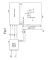
- FIG. 2 is a block diagram showing an overall configuration of the liquid crystal display device in the embodiment.
- FIG. 3 is a block diagram showing a configuration of a display control circuit in the embodiment.
- FIG. 4 is a diagram schematically showing an example of an overshoot look-up table in the embodiment.
- FIG. 5 is a diagram for describing a focused pixel group in the embodiment.
- FIG. 6 is a diagram showing the pre-correction gray scale values of the focused pixel group in the embodiment.
- FIG. 7 is a diagram showing the post-correction gray scale values of the focused pixel group in the embodiment.
- FIG. 8 is a diagram for describing an edge portion of an image in the embodiment.
- FIG. 9 is a diagram showing an example of liquid crystal response time.
- FIG. 10 is a diagram showing a change in the luminance in a focused pixel group in a conventional example.
- FIG. 11 is a diagram showing a change in the luminance in a first pixel group region in the embodiment.
- FIG. 12 is a diagram showing a change in the luminance in a second pixel group region in the embodiment.
- FIG. 13 is a diagram for describing a gray scale value correction method in a first variant of the embodiment.
- FIG. 14 is a block diagram showing a configuration of a display control circuit in a second variant of the embodiment.
- FIG. 15 is a diagram schematically showing a configuration of a gray scale correction look-up table in the second variant of the embodiment.
- FIG. 16 is a diagram for describing a gray scale value correction method in the second variant of the embodiment.
- FIG. 17 is a diagram for describing a gray scale value correction method in a third variant of the embodiment.
- FIG. 18 is a diagram showing an example in which the numbers of rows and columns of pixels forming a focused pixel group are different from each other in the third variant of the embodiment.
- FIG. 19 is a diagram showing an ideal change in luminance for when 3D display is performed in a conventional example.
- FIG. 20 is a diagram showing an actual change in luminance for when 3D display is performed in the conventional example.
- FIG. 2 is a block diagram showing an overall configuration of a liquid crystal display device according to an embodiment of the present invention.
- the liquid crystal display device is composed of a display control circuit 100 , a source driver (video signal line drive circuit) 200 , a gate driver (scanning signal line drive circuit) 300 , and a display unit 400 .
- a plurality of source bus lines (video signal lines) SL and a plurality of gate bus lines (scanning signal lines) GL are arranged in the display unit 400 .
- a pixel formation portion forming a pixel is provided at each of the intersections of the source bus lines SL and the gate bus lines GL. That is, a plurality of pixel formation portions are included in the display unit 400 .
- the plurality of pixel formation portions are arranged in a matrix, forming a pixel array.
- Each pixel formation portion includes a thin film transistor (TFT) 40 which is a switching element connected at its gate terminal to a gate bus line GL passing through a corresponding intersection, and connected at its source terminal to a source bus line SL passing through the intersection; a pixel electrode 41 connected to the drain terminal of the thin film transistor 40 ; a common electrode 42 which is a counter electrode for providing a common potential to the plurality of pixel formation portions; and a liquid crystal layer provided so as to be shared by the plurality of pixel formation portions, and sandwiched between the pixel electrode 41 and the common electrode 42 .
- TFT thin film transistor
- a pixel capacitance Cp By a liquid crystal capacitance formed by the pixel electrode 41 and the common electrode 42 , a pixel capacitance Cp is formed.
- an auxiliary capacitance is provided in parallel with the liquid crystal capacitance so as to securely hold a voltage in the pixel capacitance Cp; however, the auxiliary capacitance is not directly related to the present invention and thus the description and depiction thereof are omitted. Note that in the display unit 400 in FIG. 2 , only those components for one pixel formation portion are shown.
- the liquid crystal display device is configured to allow 3D display (stereoscopic vision).
- 3D display stereographic vision
- a frame-sequential method that alternately displays a left-eye image and a right-eye image is adopted.
- the display control circuit 100 receives from an external source an image signal DAT including left-eye gray scale data and right-eye gray scale data, and timing signals TS such as a horizontal synchronizing signal and a vertical synchronizing signal, and outputs digital video signals DV, a source start pulse signal SSP, a source clock signal SCK, and a latch strobe signal LS for controlling the operation of the source driver 200 , and a gate start pulse signal GSP and a gate clock signal GCK for controlling the operation of the gate driver 300 .
- the source driver 200 receives the digital video signals DV, the source start pulse signal SSP, the source clock signal SCK, and the latch strobe signal LS which are outputted from the display control circuit 100 , and applies drive video signals to the respective source bus lines SL.
- the digital video signals DV indicating voltages to be applied to the respective source bus lines SL are sequentially held at timing at which a pulse of the source clock signal SCK occurs.
- the held digital video signals DV are converted to analog voltages at timing at which a pulse of the latch strobe signal LS occurs.
- the converted analog voltages are simultaneously applied to all of the source bus lines SL, as drive video signals.
- the gate driver 300 repeats application of active scanning signals to the respective gate bus lines GL based on the gate start pulse signal GSP and the gate clock signal GCK which are outputted from the display control circuit 100 , in cycles of one vertical scanning period.
- the drive video signals are applied to the respective source bus lines SL, and the scanning signals are applied to the respective gate bus lines GL, by which a 3D image (stereo image) based on the image signal DAT transmitted from the external source is displayed on the display unit 400 .
- FIG. 3 is a block diagram showing a configuration of the display control circuit 100 in the present embodiment.
- the display control circuit 100 includes a timing control circuit 110 , a gray scale correction circuit 120 , an overshoot drive circuit 130 , a frame memory 140 , and an overshoot look-up table 150 .
- the timing control circuit 110 controls the operation of the gray scale correction circuit 120 and the overshoot drive circuit 130 and outputs a source start pulse signal SSP, a source clock signal SCK, a latch strobe signal LS, a gate start pulse signal GSP, and a gate clock signal GCK, based on timing signals TS transmitted from an external source.
- the gray scale correction circuit 120 performs correction on an image signal DAT to suppress occurrence of crosstalk occurring in displaying an image on the display unit 400 .
- values gray scale values
- values indicated by left-eye gray scale data and right-eye gray scale data which are included in the image signal DAT are corrected. Note that a specific gray scale value correction method will be described later.
- the overshoot drive circuit 130 performs correction on an image signal DAT2 having been subjected to the correction by the gray scale correction circuit 120 , to emphasize a temporal change of the signal (hereinafter, a method for driving liquid crystal after performing this correction is referred to as “overshoot drive”), generates write gray scale data indicating application gray scale values for the respective pixel formation portions, and outputs the write gray scale data as digital video signals DV.
- the overshoot drive is a drive method aimed at suppressing a reduction in image quality upon moving image display, which is caused by a low liquid crystal response speed.
- the overshoot drive according to a combination of an input image signal for a previous frame and an input image signal for a current frame, a higher drive voltage than a gray scale voltage corresponding to the input image signal for the current frame or a lower drive voltage than the gray scale voltage corresponding to the input image signal for the current frame is supplied to the display unit.
- the time required to reach the gray scale voltage corresponding to the input image signal for the current frame is reduced, suppressing a reduction in image quality upon moving image display.
- a liquid crystal display device adopting overshoot drive holds a look-up table (overshoot look-up table 150 ) so as to determine a drive voltage based on a combination of a gray scale value corresponding to an input image signal for a previous frame (hereinafter, referred to as a “previous-frame gray scale value”) and a gray scale value corresponding to an input image signal for a current frame (hereinafter, referred to as a “current-frame gray scale value”).
- FIG. 4 is a diagram schematically showing an example of the overshoot look-up table 150 held in a liquid crystal display device capable of performing 256 gray scale display. In FIG.
- the numerical values described in the leftmost column indicate previous-frame gray scale values
- the numerical values described in the topmost row indicate current-frame gray scale values.
- a numerical value described at a location where a row and a column intersect indicates a gray scale value (hereinafter, referred to as an “application gray scale value”) corresponding to a drive voltage which is determined based on a combination of a previous-frame gray scale value and a current-frame gray scale value. For example, when the previous-frame gray scale value is “64” and the current-frame gray scale value is “128”, the application gray scale value is “155”. In addition, for example, when the previous-frame gray scale value is “160” and the current-frame gray scale value is “64”, the application gray scale value is “20”.
- a higher drive voltage than a gray scale voltage corresponding to an input image signal for a current frame or a lower drive voltage than the gray scale voltage corresponding to the input image signal for the current frame is applied to the liquid crystal.
- gray scale value correction is performed such that four pixels (pixels of two rows ⁇ two columns) having the same gray scale value are considered one collective group.
- the four pixels are referred to as a “focused pixel group”
- correction is performed on the gray scale values of the respective pixels in the focused pixel group such that brightness corresponding to the original gray scale value is visually recognized in a pseudo manner at the entire focused pixel group.
- a pixel arranged in the upper left position is referred to as Pix (1, 1)
- a pixel arranged in the lower left position is referred to as Pix (1, 2)
- a pixel arranged in the upper right position is referred to as Pix (2, 1)
- a pixel arranged in the lower right position is referred to as Pix (2, 2).
- first pixel group pixels whose post-correction gray scale values are the same between a left-eye image and a right-eye image
- second pixel group pixels whose post-correction gray scale values are different between the left-eye image and the right-eye image.
- Pix (1, 2) and Pix (2, 1) serve as the first pixel group
- Pix (1, 1) and Pix (2, 2) serve as the second pixel group.
- the pre-correction gray scale value of the focused pixel group is “12” for the left-eye image, and is “16” for the right-eye image.
- an average value between a pre-correction gray scale value of the left-eye image and a pre-correction gray scale value of the right-eye image is a post-correction gray scale value of the first pixel group. Therefore, in this example, the post-correction gray scale values of Pix (1, 2) and Pix (2, 1) which serve as the first pixel group are “14” which is an average value between “12” and “16”.
- the post-correction gray scale values of the second pixel group are determined such that, for both of the left-eye image and the right-eye image, an average gray scale value of the entire focused pixel group is not changed between before and after the correction. Therefore, in this example, the post-correction gray scale values of Pix (1, 1) and Pix (2, 2) which serve as the second pixel group are “10” for the left-eye image and are “18” for the right-eye image. In the above-described manner, in this example, the post-correction gray scale values of the focused pixel group are such as those shown in FIG. 7 .
- the gray scale values of Pix (1, 2) and Pix (2, 1) are corrected from “12” to “14”, and the gray scale values of Pix (1, 1) and Pix (2, 2) are corrected from “12” to “10”.
- the gray scale values of Pix (1, 2) and Pix (2, 1) are corrected from “16” to “14”, and the gray scale values of Pix (1, 1) and Pix (2, 2) are corrected from “16” to “18”.
- the pre-correction gray scale value of the focused pixel group is GL for the left-eye image and is GR for the right-eye image.
- a post-correction gray scale value GM of the first pixel group for both of the left-eye image and the right-eye image is obtained by the following equation (1).
- GM ( GL+GR )/2 (1)
- a post-correction gray scale value GLa of the second pixel group for the left-eye image is obtained by the following equation (2)
- a post-correction gray scale value GRa of the second pixel group for the right-eye image is obtained by the following equation (3).
- GLa 2 GL ⁇ GM (2)
- GRa 2 GR ⁇ GM (3)
- the pre-correction gray scale values of four pixels included in each group are not always identical. For example, at an edge portion of an image, as shown in FIG. 8 , a plurality of pixels having different gray scale values are present in a group. Gray scale value correction according to the present invention is not performed on such a portion.
- the four pixels when four pixels (pixels of two rows ⁇ two columns) having the same gray scale value are focused, the four pixels are divided into two pixels (first pixel group) whose post-correction gray scale values are the same between a left-eye image and a right-eye image, and two pixels (second pixel group) whose post-correction gray scale values are different between the left-eye image and the right-eye image.
- first pixel group since the luminance does not change at switching timing between left-eye image display and right-eye image display, crosstalk or flicker does not occur.
- the gray scale values of the respective pixels are corrected such that an average gray scale value of all of the four pixels is not changed between before and after the correction.
- FIG. 9 is a diagram showing an example of liquid crystal response time.
- the numerical values described in the leftmost column indicate previous-frame gray scale values
- the numerical values described in the topmost row indicate current-frame gray scale values.
- a numerical value described at a location where a row and a column intersect indicates response time for when the gray scale value changes from a previous-frame gray scale value to a current-frame gray scale value.
- the response time is 6.4 milliseconds when the current-frame gray scale value is “96”, and the response time is 4.1 milliseconds when the current-frame gray scale value is “128”. From this fact, it is grasped that the greater the difference between the previous-frame gray scale value and the current-frame gray scale value is, the shorter the response time is (the higher the response speed is).
- the liquid crystal response time is reduced compared to before the correction.
- the occurrence of crosstalk is suppressed.
- luminance corresponding to a gray scale value n is represented by Lu(n).
- the pre-correction gray scale value of the focused pixel group is “12” for the left-eye image and is “16” for the right-eye image. If image display is performed based on these pre-correction gray scale values, then the gray scale values uniformly change in all pixels in the focused pixel group (see “before correction” in FIG. 1 ) upon switching from a left-eye image display period to a right-eye image display period.
- the luminance changes as shown in FIG. 10 .
- the gray scale values are maintained for some pixels (first pixel group) and the gray scale values greatly change for the remaining pixels (second pixel group) compared to before the correction (see “after correction” in FIG. 1 ) upon switching from a left-eye image display period to a right-eye image display period.
- the luminance is constant as shown in FIG. 11 in the first pixel group region, and the luminance changes as shown in FIG. 12 in the second pixel group region.
- response time TD2 in the present embodiment is smaller than response time TD1 in the conventional example.
- FIG. 13 is a diagram for describing a gray scale value correction method in a first variant of the above-described embodiment.
- gray scale value correction is not performed on a left-eye image.
- the post-correction gray scale value of a first pixel group is the gray-scale value of the left-eye image
- the post-correction gray scale value of a second pixel group is determined such that an average gray scale value of the entire focused pixel group is not changed between before and after the correction.
- the luminance does not change in a first pixel group region, and the luminance greatly changes in a second pixel group region compared to conventional cases (see FIG. 13 ). Therefore, a reduction in image quality caused by crosstalk is suppressed.
- the gray scale values for only one of the left-eye image and the right-eye image should be changed upon switching between left-eye image display and right-eye image display. Hence, the load of the process of correcting the gray scale values is reduced.
- FIG. 14 is a block diagram showing a configuration of a display control circuit 101 in a second variant of the above-described embodiment.
- a gray scale correction look-up table 160 is provided in the display control circuit 101 .
- FIG. 15 is a diagram schematically showing a configuration of the gray scale correction look-up table 160 .
- the numerical values described in the leftmost column indicate the pre-correction gray scale values (first input values) of the focused pixel group for the left-eye image
- the numerical values described in the topmost row indicate the pre-correction gray scale values (second input values) of the focused pixel group for the right-eye image.
- a numerical value described at a location where a row and a column intersect indicates a post-correction gray scale value (output value) of the first pixel group.
- gray scale value correction is performed as follows. First, as in the above-described embodiment, a first pixel group and a second pixel group are determined. Then, with a pre-correction gray scale value of a left-eye image being a first input value and a pre-correction gray scale value of a right-eye image being a second input value, a post-correction gray scale value of the first pixel group is determined from the gray scale correction look-up table 160 . As in the above-described embodiment, the post-correction gray scale values of the second pixel group are determined such that, for both of the left-eye image and the right-eye image, an average gray scale value of the entire focused pixel group is not changed between before and after the correction.
- the post-correction gray scale value of the first pixel group is determined to be “13”.
- the post-correction gray scale value of the second pixel group is determined to be “11” for the left-eye image and is determined to be “19” for the right-eye image.
- the post-correction gray scale values of the first pixel group can be previously set in the look-up table such that the liquid crystal response speed of the second pixel group gets higher.
- a focused pixel group is composed of four pixels, and two of the four pixels serve as a first pixel group and the remaining two pixels serve as a second pixel group
- the present invention is not limited thereto.
- a focused pixel group may be composed of nine pixels.
- two-thirds of the pixels in a focused pixel group may serve as a first pixel group, and one-thirds of the pixels in the focused pixel group may serve as a second pixel group.
- the number of pixels forming a focused pixel group or the component ratio between a first pixel group and a second pixel group in a focused pixel group is not particularly limited.
- the numbers of rows and columns of pixels forming a focused pixel group may be different from each other.
Landscapes
- Engineering & Computer Science (AREA)
- Physics & Mathematics (AREA)
- Computer Hardware Design (AREA)
- General Physics & Mathematics (AREA)
- Theoretical Computer Science (AREA)
- Chemical & Material Sciences (AREA)
- Crystallography & Structural Chemistry (AREA)
- Multimedia (AREA)
- Signal Processing (AREA)
- Control Of Indicators Other Than Cathode Ray Tubes (AREA)
Abstract
Description
- [Patent Document 1] Japanese Patent Application Laid-Open No. 2005-242026
GM=(GL+GR)/2
where GL represents a pre-correction gray scale value for the left-eye gray scale data, and GR represents a pre-correction gray scale value for the right-eye gray scale data.
GM=(GL+GR)/2 (1)
Then, a post-correction gray scale value GLa of the second pixel group for the left-eye image is obtained by the following equation (2), and a post-correction gray scale value GRa of the second pixel group for the right-eye image is obtained by the following equation (3).
GLa=2GL−GM (2)
GRa=2GR−GM (3)
-
- 100 and 101: DISPLAY CONTROL CIRCUIT
- 110: TIMING CONTROL CIRCUIT
- 120: GRAY SCALE CORRECTION CIRCUIT
- 130: OVERSHOOT DRIVE CIRCUIT
- 140: FRAME MEMORY
- 150: OVERSHOOT LOOK-UP TABLE
- 160: GRAY SCALE CORRECTION LOOK-UP TABLE
- 200: SOURCE DRIVER (VIDEO SIGNAL LINE DRIVE CIRCUIT)
- 300: GATE DRIVER (SCANNING SIGNAL LINE DRIVE CIRCUIT)
- 400: DISPLAY UNIT
Claims (6)
GM=(GL+GR)/2
Applications Claiming Priority (3)
| Application Number | Priority Date | Filing Date | Title |
|---|---|---|---|
| JP2011-228701 | 2011-10-18 | ||
| JP2011228701 | 2011-10-18 | ||
| PCT/JP2012/076280 WO2013058158A1 (en) | 2011-10-18 | 2012-10-11 | Display control circuit, liquid crystal display device equipped with same and display control method |
Publications (2)
| Publication Number | Publication Date |
|---|---|
| US20140267463A1 US20140267463A1 (en) | 2014-09-18 |
| US9344709B2 true US9344709B2 (en) | 2016-05-17 |
Family
ID=48140806
Family Applications (1)
| Application Number | Title | Priority Date | Filing Date |
|---|---|---|---|
| US14/350,419 Expired - Fee Related US9344709B2 (en) | 2011-10-18 | 2012-10-11 | Display control circuit, liquid crystal display device including the same, and display control method |
Country Status (2)
| Country | Link |
|---|---|
| US (1) | US9344709B2 (en) |
| WO (1) | WO2013058158A1 (en) |
Families Citing this family (4)
| Publication number | Priority date | Publication date | Assignee | Title |
|---|---|---|---|---|
| CN106461990B (en) * | 2014-06-04 | 2018-03-20 | 堺显示器制品株式会社 | Liquid crystal display device and display method |
| CN114189670B (en) * | 2020-09-15 | 2024-01-23 | 北京小米移动软件有限公司 | Display method, display device, display apparatus and storage medium |
| US20220337807A1 (en) * | 2021-04-15 | 2022-10-20 | Google Llc | Crosstalk compensation for 3d lightfield displays |
| WO2023130444A1 (en) * | 2022-01-10 | 2023-07-13 | 京东方科技集团股份有限公司 | Driving method for display panel, and display apparatus |
Citations (13)
| Publication number | Priority date | Publication date | Assignee | Title |
|---|---|---|---|---|
| US20050190610A1 (en) * | 2004-02-26 | 2005-09-01 | Tomoo Furukawa | Driving system for display device |
| US20080316303A1 (en) * | 2007-06-08 | 2008-12-25 | Joseph Chiu | Display Device |
| US20110001806A1 (en) * | 2009-07-03 | 2011-01-06 | Sony Corporation | Image displaying device and image displaying system |
| US20110037829A1 (en) * | 2009-08-11 | 2011-02-17 | Sony Corporation | Display device, display method and computer program |
| US20110090321A1 (en) * | 2009-10-21 | 2011-04-21 | Sony Corporation | Display device, display method and computer program |
| US20110157161A1 (en) * | 2009-12-24 | 2011-06-30 | Samsung Electronics Co., Ltd. | Method of displaying stereo-scopic image and display apparatus for performing the same |
| US20110210964A1 (en) * | 2007-06-08 | 2011-09-01 | Reald Inc. | Stereoscopic flat panel display with synchronized backlight, polarization control panel, and liquid crystal display |
| US20110310090A1 (en) * | 2010-06-22 | 2011-12-22 | Euitae Kim | Data modulation method and liquid crystal display device using the same |
| US20110316849A1 (en) * | 2010-06-29 | 2011-12-29 | Canon Kabushiki Kaisha | Image processing apparatus for displaying image on display unit and control method thereof |
| US20120007858A1 (en) * | 2010-07-07 | 2012-01-12 | Baek Heumeil | Stereoscopic image display device and driving method thereof |
| US20120007895A1 (en) * | 2010-07-08 | 2012-01-12 | Kim Kiltae | Stereoscopic image display and driving method thereof |
| US20120147161A1 (en) * | 2010-12-10 | 2012-06-14 | Kim Kiltae | Stereoscopic image display and driving method thereof |
| US20130128019A1 (en) * | 2010-08-09 | 2013-05-23 | Sharp Kabushiki Kaisha | Display device, display control method, display control program, and computer readable recording medium |
Family Cites Families (3)
| Publication number | Priority date | Publication date | Assignee | Title |
|---|---|---|---|---|
| JP3760903B2 (en) * | 2002-08-22 | 2006-03-29 | セイコーエプソン株式会社 | Image display device |
| JP4743837B2 (en) * | 2005-01-13 | 2011-08-10 | ルネサスエレクトロニクス株式会社 | Controller / driver, liquid crystal display device using the same, and liquid crystal driving method |
| JP4769003B2 (en) * | 2005-03-28 | 2011-09-07 | パナソニック株式会社 | Display device |
-
2012
- 2012-10-11 WO PCT/JP2012/076280 patent/WO2013058158A1/en not_active Ceased
- 2012-10-11 US US14/350,419 patent/US9344709B2/en not_active Expired - Fee Related
Patent Citations (14)
| Publication number | Priority date | Publication date | Assignee | Title |
|---|---|---|---|---|
| JP2005242026A (en) | 2004-02-26 | 2005-09-08 | Sharp Corp | Display device drive system |
| US20050190610A1 (en) * | 2004-02-26 | 2005-09-01 | Tomoo Furukawa | Driving system for display device |
| US20110210964A1 (en) * | 2007-06-08 | 2011-09-01 | Reald Inc. | Stereoscopic flat panel display with synchronized backlight, polarization control panel, and liquid crystal display |
| US20080316303A1 (en) * | 2007-06-08 | 2008-12-25 | Joseph Chiu | Display Device |
| US20110001806A1 (en) * | 2009-07-03 | 2011-01-06 | Sony Corporation | Image displaying device and image displaying system |
| US20110037829A1 (en) * | 2009-08-11 | 2011-02-17 | Sony Corporation | Display device, display method and computer program |
| US20110090321A1 (en) * | 2009-10-21 | 2011-04-21 | Sony Corporation | Display device, display method and computer program |
| US20110157161A1 (en) * | 2009-12-24 | 2011-06-30 | Samsung Electronics Co., Ltd. | Method of displaying stereo-scopic image and display apparatus for performing the same |
| US20110310090A1 (en) * | 2010-06-22 | 2011-12-22 | Euitae Kim | Data modulation method and liquid crystal display device using the same |
| US20110316849A1 (en) * | 2010-06-29 | 2011-12-29 | Canon Kabushiki Kaisha | Image processing apparatus for displaying image on display unit and control method thereof |
| US20120007858A1 (en) * | 2010-07-07 | 2012-01-12 | Baek Heumeil | Stereoscopic image display device and driving method thereof |
| US20120007895A1 (en) * | 2010-07-08 | 2012-01-12 | Kim Kiltae | Stereoscopic image display and driving method thereof |
| US20130128019A1 (en) * | 2010-08-09 | 2013-05-23 | Sharp Kabushiki Kaisha | Display device, display control method, display control program, and computer readable recording medium |
| US20120147161A1 (en) * | 2010-12-10 | 2012-06-14 | Kim Kiltae | Stereoscopic image display and driving method thereof |
Non-Patent Citations (1)
| Title |
|---|
| Official Communication issued in International Patent Application No. PCT/JP2012/076280, mailed on Dec. 18, 2012. |
Also Published As
| Publication number | Publication date |
|---|---|
| WO2013058158A1 (en) | 2013-04-25 |
| US20140267463A1 (en) | 2014-09-18 |
Similar Documents
| Publication | Publication Date | Title |
|---|---|---|
| US9330617B2 (en) | Method of driving a display panel and display apparatus for performing the same | |
| US9083965B2 (en) | Stereoscopic display device | |
| US9196184B2 (en) | Method of driving display panel and display apparatus for performing the same | |
| US9105227B2 (en) | Electro-optical device and electronic apparatus | |
| US10102811B2 (en) | Method of displaying three-dimensional image and display apparatus using the same | |
| US8179356B2 (en) | Method for driving liquid crystal display with inserting gray image | |
| CN102855853A (en) | Three dimensional image display device and driving method thereof | |
| US10509232B2 (en) | Stereoscopic image display device using spatial-divisional driving and method of driving the same | |
| JP2012189629A (en) | Display device and display control method | |
| US9344709B2 (en) | Display control circuit, liquid crystal display device including the same, and display control method | |
| CN104253987B (en) | Stereoscopic image display and driving method thereof | |
| TWI469130B (en) | Stereo display system | |
| KR20130092906A (en) | Display device and driving method thereof | |
| US9013459B2 (en) | Liquid crystal display device | |
| US9305507B2 (en) | Liquid crystal display device capable of performing 2D display and 3D display, and drive method thereof | |
| US20120026204A1 (en) | Three-dimensional display and driving method thereof | |
| US9324255B2 (en) | Electro-optic device and electronic apparatus | |
| US9161022B2 (en) | Electro-optical device, method of driving electro-optical device, and electronic apparatus | |
| KR101846372B1 (en) | 3D image display device and method of driving the same | |
| JP2011075668A (en) | Image display device and method for driving the same | |
| US20150130854A1 (en) | Liquid-crystal display device and method for driving same | |
| US9473765B2 (en) | Three-dimensional shutter glasses and grayscale driving method thereof | |
| JP2013205462A (en) | Liquid crystal display device | |
| KR101696255B1 (en) | liquid crystal display device and method of driving the same | |
| WO2014030286A1 (en) | Liquid crystal display device |
Legal Events
| Date | Code | Title | Description |
|---|---|---|---|
| AS | Assignment |
Owner name: SHARP KABUSHIKI KAISHA, JAPAN Free format text: ASSIGNMENT OF ASSIGNORS INTEREST;ASSIGNOR:YAMAKAWA, RYO;REEL/FRAME:032626/0503 Effective date: 20140312 |
|
| STCF | Information on status: patent grant |
Free format text: PATENTED CASE |
|
| CC | Certificate of correction | ||
| FEPP | Fee payment procedure |
Free format text: PAYOR NUMBER ASSIGNED (ORIGINAL EVENT CODE: ASPN); ENTITY STATUS OF PATENT OWNER: LARGE ENTITY |
|
| FEPP | Fee payment procedure |
Free format text: MAINTENANCE FEE REMINDER MAILED (ORIGINAL EVENT CODE: REM.); ENTITY STATUS OF PATENT OWNER: LARGE ENTITY |
|
| LAPS | Lapse for failure to pay maintenance fees |
Free format text: PATENT EXPIRED FOR FAILURE TO PAY MAINTENANCE FEES (ORIGINAL EVENT CODE: EXP.); ENTITY STATUS OF PATENT OWNER: LARGE ENTITY |
|
| STCH | Information on status: patent discontinuation |
Free format text: PATENT EXPIRED DUE TO NONPAYMENT OF MAINTENANCE FEES UNDER 37 CFR 1.362 |
|
| FP | Lapsed due to failure to pay maintenance fee |
Effective date: 20200517 |