US9342639B1 - Method of hierarchical timing closure of VLSI circuits using partially disruptive feedback assertions - Google Patents
Method of hierarchical timing closure of VLSI circuits using partially disruptive feedback assertions Download PDFInfo
- Publication number
- US9342639B1 US9342639B1 US14/623,835 US201514623835A US9342639B1 US 9342639 B1 US9342639 B1 US 9342639B1 US 201514623835 A US201514623835 A US 201514623835A US 9342639 B1 US9342639 B1 US 9342639B1
- Authority
- US
- United States
- Prior art keywords
- timing
- component
- assertions
- slack
- feedback
- Prior art date
- Legal status (The legal status is an assumption and is not a legal conclusion. Google has not performed a legal analysis and makes no representation as to the accuracy of the status listed.)
- Expired - Fee Related
Links
Images


Classifications
-
- G—PHYSICS
- G06—COMPUTING OR CALCULATING; COUNTING
- G06F—ELECTRIC DIGITAL DATA PROCESSING
- G06F30/00—Computer-aided design [CAD]
- G06F30/30—Circuit design
- G06F30/32—Circuit design at the digital level
- G06F30/33—Design verification, e.g. functional simulation or model checking
- G06F30/3315—Design verification, e.g. functional simulation or model checking using static timing analysis [STA]
-
- G—PHYSICS
- G06—COMPUTING OR CALCULATING; COUNTING
- G06F—ELECTRIC DIGITAL DATA PROCESSING
- G06F30/00—Computer-aided design [CAD]
- G06F30/30—Circuit design
- G06F30/32—Circuit design at the digital level
- G06F30/33—Design verification, e.g. functional simulation or model checking
- G06F30/3308—Design verification, e.g. functional simulation or model checking using simulation
- G06F30/3312—Timing analysis
-
- G06F17/5031—
-
- G06F17/5081—
-
- G—PHYSICS
- G06—COMPUTING OR CALCULATING; COUNTING
- G06F—ELECTRIC DIGITAL DATA PROCESSING
- G06F30/00—Computer-aided design [CAD]
- G06F30/30—Circuit design
- G06F30/39—Circuit design at the physical level
- G06F30/398—Design verification or optimisation, e.g. using design rule check [DRC], layout versus schematics [LVS] or finite element methods [FEM]
-
- G06F17/5068—
-
- G—PHYSICS
- G06—COMPUTING OR CALCULATING; COUNTING
- G06F—ELECTRIC DIGITAL DATA PROCESSING
- G06F2119/00—Details relating to the type or aim of the analysis or the optimisation
- G06F2119/12—Timing analysis or timing optimisation
-
- G—PHYSICS
- G06—COMPUTING OR CALCULATING; COUNTING
- G06F—ELECTRIC DIGITAL DATA PROCESSING
- G06F30/00—Computer-aided design [CAD]
- G06F30/30—Circuit design
- G06F30/39—Circuit design at the physical level
Definitions
- the present invention generally relates to the field of Electronic Design Automation (EDA), and more particularly, to the generation and consumption of feedback timing assertions from hierarchical designs for timing closure of design components.
- EDA Electronic Design Automation
- Static Timing Analysis is a key step in the design of high speed Very Large Scale Integrated (VLSI) circuits.
- STA is used to verify that a VLSI circuit-design performs correctly at a required frequency before it is released for chip manufacturing.
- a circuit-design must be timing closed prior to manufacturing.
- Timing closure refers to the process of designing and optimizing a circuit such that applied electrical signals can traverse through the circuit within specified timing constraints.
- STA guides and validates the completion of timing closure.
- a circuit-design is represented as a timing graph; the points in the design where timing information is desired constitute the nodes or timing points of this graph, while electrical or logic connections between these nodes are represented as timing arcs of the graph.
- STA is performed typically at the logic gate level using lookup-table based gate timing libraries and involves some runtime expensive circuit simulation for timing calculation of wires and gates using current source model based timing libraries.
- ASIC Application Specific Integrated Circuit
- Performance centric designs especially microprocessor designs, include custom circuit designed components to achieve aggressive frequency targets and can contain upwards of one billion transistors. STA of these designs ideally like to employ circuit simulators for obtaining accurate timing calculations.
- the run-time intensive nature of circuit simulation is impractical for large designs, especially where timing runs are made daily during the design cycle of the chip. In essence, static timing analysis of modern large circuits as a single flattened design is run-time prohibitive. This has led to the development of a hierarchical timing flow wherein a circuit design is partitioned into components.
- a component may be partitioned further into sub-components in a recursive fashion.
- a typical microprocessor design is partitioned into several components called cores, each core is partitioned into components termed units, and each unit is partitioned into components termed macros.
- a core level of hierarchy can contain a set of units connected using wires and additional gates that may not be part of any component.
- a unit level of hierarchy can contain a set of macros connected using wires and additional gates that may not be part of any component.
- the term “component” will be used in this invention to refer to a sub-component or component (e.g. a macro, unit, or the core).
- FIG. 1 it illustrates a unit component containing two sub-components (macros), namely, Macro-1 and Macro-2, and additional gates and wires.
- STA and timing closure for each component is performed in isolation or “out of context” (OOC).
- OOC isolation or “out of context”
- the component is not connected to any other part of the circuit outside its scope.
- a timing abstract could either be a pruned version of the component or a single gate timing model of the component.
- internal latch to latch paths of the component are deleted from the design in the abstract model.
- the primary objective of creating an abstract is to make the timing model of the component simpler.
- Components are next represented using their abstracts at the parent level(s) of hierarchy.
- the hierarchical timing approach enables fast timing analysis and productivity at the parent level, since the abstract models are simpler and allow re-use.
- the benefits are significantly highlighted when multiple instances of a component are used at a level since the flow avoids separate static timing analysis for each instance of the full component.
- FIG. 2 illustrates a component 200 with two primary inputs and one primary output pin.
- the component contains three latches, namely, L 1 , L 2 and L 3 .
- This component is timed at the out-of-context level (not connected to the parent level of hierarchy), and then an abstract 201 of the component is generated.
- the internal latch to latch path from L 1 to L 3 is pruned in the abstract model.
- a component's abstract is typically generated post timing closure and is then used at the parent level of hierarchy.
- timing closure of the component is dependent on the timing assertions at its boundary (primary input and primary output) pins.
- timing closure for a data path starting from a primary input (PI) of a component and leading to either a latch or a primary output (PO) is therefore dependent on when the electrical signal reaches the PI, which in turn is known accurately only at the parent level of hierarchy.
- PI primary input
- PO primary output
- the alternative approach involves a feedback assertion process, wherein multiple iterations of abstracts are generated during the chip design life-cycle.
- assertions for the component being represented by its abstract are generated, and are subsequently used to perform STA and timing closure of the component.
- This is followed by the generation of a new abstract for the component post timing closure using assertions from the prior version of the abstract.
- the new abstract is then used for the next iteration of feedback assertion generation.
- FIG. 3 illustrates a parent level of hierarchy wherein component 300 contains an abstract of a sub-component.
- a set of two numbers is shown on certain pins in the design, and denote the ⁇ arrival-time (AT), required-arrival-time (RAT) ⁇ , respectively, for the corresponding pin.
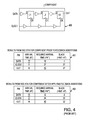
- FIG. 4 depicts the out-of-context timing computation and use of feedback assertions for a component 400 .
- the abstract of this component is assumed to be the one used at the parent level of hierarchy 300 in FIG. 3 .
- the component 400 Prior to feedback assertions, the component 400 is assumed to have been timed using default (or older) assertions which are highlighted as underlined values in table 401 .
- the table 401 contains all timing information computed using these assertions as well. The timing values are based on the assumptions made in the prior section, namely, the path delay from CLOCK to OUT is 16 units, and the RAT of pin DATA is 10 units greater than the AT of pin CLOCK.
- the main advantage of the feedback assertion process is that the most accurate data and clock signal timings at the boundary pins of the component's abstract (as observed during STA at a parent level of hierarchy) are used for timing closure of the component during its “out of context” timing. This enables accurate timing closure of boundary paths of the component.
- a new feedback assertion for a clock PI of the component also impacts the timing of internal latch to latch paths, which may be undesirable.
- applying feedback assertions 302 in FIG. 3 to component 400 in FIG. 4 updates the AT of pins CLOCK and OUT as shown in table 401 to new values as shown in table 402 .
- a method of not using the new assertions for the clock PI pins, but using new assertions for non-clock PI pins will result in inconsistent timing of boundary paths, and may even lead to a false illusion of timing closure eventually resulting in a faulty manufactured chip design.
- a method of not using feedback assertions at all for out-of-context STA of the component is equally susceptible to yielding a faulty manufactured chip. This indicates a need for a method of generating feedback assertions that guarantee timing non-disruptions to the internal latch to latch paths, yet maintain the accuracy of timing closure in the boundary paths of the component.
- an embodiment provides a method and a system for generating and consumption of feedback assertions that do not disrupt timing of internal latch to latch paths during out of context timing of a component during hierarchical timing.
- it provides a method and a system for capturing feedback assertions in the form of slack to be applied during out-of-context timing.
- a method and a system for computing one of arrival time or required arrival time dynamically to be applied as an assertion from a captured slack assertion is provided.
- a method and a system achieve the generation and consumption of statistical feedback assertions that does not disrupt timing of internal latch to latch paths during out-of-context statistical timing of a component during hierarchical statistical timing.
- the generated assertions guarantee timing non-disruption in certain sections of the design component being timed with the assertions, thereby improving chip design and optimization productivity prior to chip manufacturing.
- FIG. 1 shows a prior art illustrative unit component of a hierarchical chip design containing macro sub-components.
- FIG. 2 illustrates the prior art illustrative generation of a timing abstract for a component containing two inputs, one output and three latches.
- FIG. 3 illustrates a prior art illustrative structure and timing of an abstract at its parent level of hierarchy, and generated feedback assertions.
- FIG. 4 illustrates a prior art illustrative structure and timing of a component out-of-context, and the updated time post application of feedback assertions.
- FIG. 5 is a flowchart illustrating the steps of generating feedback assertions in the form of slack, in accordance of an embodiment.
- FIG. 6 illustrates capturing of feedback assertions in the form of slack for an abstract at its parents level of hierarchy, according to an embodiment.
- FIG. 7 is a flowchart illustrating the steps for consuming the feedback assertions captured in a slack form for the out-of-context timing of a component, according to an embodiment.
- FIG. 8 illustrates dynamically generated assertions from captured feedback assertions for a component and its resulting timing, according to an embodiment.
- FIG. 5 is a flow diagram illustrating one embodiment of a method 500 for generating feedback assertions for a sub-component at the parent level of hierarchy for that sub-component.
- the method 500 is initialized in step 501 .
- a component of a hierarchical chip design is read in along with the timing models for all included sub-components and gates, as well as timing assertions.
- Each included sub-component could be either a detailed partition containing gates and wires, or an abstract model of the sub-component that it replaces at the current level of hierarchy.
- Gates and abstract timing models examples include industry standard timing models like Liberty, ECSM and CCS.
- the design may also include transistor level logic which requires a circuit simulator to obtain delay and slew (or waveform) information during static timing analysis.
- step 503 static timing analysis (STA) of the component is performed, wherein timing quantities like arrival times (AT) and required arrival times (RAT) are computed for all desired pins in the design. As part of STA, slacks are also obtained at all desired pins.
- STA static timing analysis
- This step may include traditional static timing analysis related steps like coupling analysis, common path pessimism reduction, and report generation.
- step 504 feedback assertions for each desired unique sub-component type is generated.
- the slack on each output pin of the sub-component is captured.
- the slack for each non-clock input pin of the sub-component is also captured.
- the traditional method of capturing the AT for each input pin, and the RAT for each output pin, respectively, is performed optionally.
- Other aspects of feedback assertions, including capturing the slew on input pins and effective loads on outputs pins are performed in the traditional fashion.
- feedback assertions on the boundary (input and output) pins are captured for each phase individually.
- a reduced set of assertions may be captured by filtering the assertions for non-critical clock phases.
- the captured slack could correspond to a pre-decided instance of the sub-component.
- the decision to choose a critical sub-component could be based on slack.
- the worst slack across multiple instances of a given boundary pin of a given sub-component type is captured as the feedback assertion.
- the method 500 for generating feedback assertions for the sub-component terminates in step 505 .
- FIG. 6 illustrates a parent level of hierarchy wherein component 600 contains an abstract of a sub-component.
- the design illustrated in this figure and the timing information shown is identical to that in FIG. 3 .
- traditional feedback assertions for the abstract as shown in table 302 of FIG. 3 does not contain any slack information, in one embodiment as described in the flow-diagram 500 of FIG. 5 , the feedback assertions include slack information for all output and non-clock input pins as shown in table 601 of FIG. 6 .
- the AT and RAT on some boundary pins are captured as well.
- FIG. 7 is a flow diagram illustrating one embodiment of a method 700 for hierarchical timing analysis at the out-of-context (OOC) level of a component using feedback slack assertions generated from the component's parent level of hierarchy.
- the method 700 is initialized in step 701 .
- step 702 the component circuit is read along with the timing models for all gates (or transistors) and wires in the component. Default or older timing assertions for the circuit are also read in during this step.
- Static timing analysis (STA) of the circuit is next performed in step 703 , wherein timing quantities like delays and slews are propagated throughout the timing graph to obtain arrival times at the primary outputs. Required arrival times are propagated in a traditional manner backwards from the primary outputs to the primary inputs, and subsequently slacks are obtained at all desired timing pins.
- This step may include traditional static timing analysis related steps like coupling analysis, common path pessimism reduction, and report generation.
- Generated slack based feedback assertions are next loaded in step 704 .
- the existing RAT at this pin RAT′ is used in conjunction with the feedback assertion slack SLK* I to generate a new arrival time (AT) assertion: AT* I .
- AT arrival time
- the dynamically generated AT assertion is thus obtained by subtracting the feedback slack assertion from the computed RAT at the pin.
- this example illustrates timing computation in the late mode, wherein slack is defined as (RAT ⁇ AT).
- slack is defined as (AT ⁇ RAT)
- the calculation is modified accordingly.
- the dynamically generated RAT assertion is thus obtained by adding the feedback slack assertion to the computed AT on the pin.
- slack is defined as (RAT ⁇ AT).
- AT ⁇ RAT early mode of calculation
- the calculation is modified accordingly.
- the design contains a combinational path from a non-clock input to an output, only one end of the path is updated with a new assertion. As an example, either just the input would be updated with a new AT, or the output would be updated with a new RAT.
- step 705 a final timing analysis is performed in step 705 to ensure the timing of the design is update. Additional steps of timing including coupling analysis, common path pessimism removal and report generation may be performed at this stage. A new abstract is also generated at this step. The method terminates in step 706 .
- FIG. 8 illustrates the out-of-context timing computation and use of slack based feedback assertions for a component 800 .
- the scenario is identical to that of component 400 in FIG. 4 .
- the abstract of this component is assumed to be the one used at the parent level of hierarchy 600 in FIG. 6 .
- the component 800 Prior to feedback assertions, the component 800 is assumed to have been timed using default (or older) assertions which are highlighted as underlined values in table 801 .
- the table 801 contains all timing information computed using these assertions as well, and is identical to table 401 of FIG. 4 .
- slack based feedback assertions as illustrated in table 601 of FIG. 6
- the timing at various pins in the design is updated as follows.
- the slack based feedback assertion does not capture slack at the parent level of hierarchy. Instead, traditional feedback assertions are generated.
- OOC out-of-context
- traditional feedback assertions are loaded traditionally and timing is performed to obtain slacks at boundary pins. At this stage, these slacks are captured as slack based feedback assertions.
- This embodiment facilitates capturing slack based feedback assertions at the OOC level instead of the parent level. This method is advantageous when traditional (non slack based) feedback assertions are already available, and it is undesirable to generate (slack based) feedback assertions again at the parent level of hierarchy.
- the traditional feedback assertions from the parent level are loaded in an OOC run of the abstract of the component instead of the detailed component, and slack based feedback assertions are generated as described above.
- Flow 700 as illustrated in FIG. 7 can next be applied as described earlier.
- the results of the preliminary timing analysis using default or older assertions may be performed using the abstract of the OOC component instead of the detailed component. This would enable obtaining quantities like RAT I and AT O as shown in E.Q. (1) and E.Q. (2), respectively, more efficiently.
- statistical slack based feedback assertions may be generated and used.
- the slacks captured during timing (either multi-corner or statistical) at the parent level of hierarchy would be captured in a variability aware fashion, an example of which is statistical slack.
- new statistical arrival times and statistical required arrival times would be dynamically generated based on E.Q. (1) and E.Q. (2), wherein each timing quantity like AT, RAT and slack is a statistical quantity instead of a deterministic value. Addition and subtraction of statistical quantities are performed traditionally.
- one or more steps of the methods described herein may include a storing, displaying and/or outputting step as required for a particular application.
- any data, records, fields, and/or intermediate results discussed in the methods can be stored, displayed, and/or outputted to another device as required for a particular application.
Landscapes
- Engineering & Computer Science (AREA)
- Computer Hardware Design (AREA)
- Physics & Mathematics (AREA)
- Theoretical Computer Science (AREA)
- Evolutionary Computation (AREA)
- Geometry (AREA)
- General Engineering & Computer Science (AREA)
- General Physics & Mathematics (AREA)
- Design And Manufacture Of Integrated Circuits (AREA)
Abstract
Description
RATI−AT*I=SLK*I. Therefore:
AT*I=RATI−SLK*I. E.Q. (1)
RAT*O−ATO=SLK*O. Therefore:
RAT*O=ATO+SLK*O. E.Q. (2)
AT*DATA=RATDATA−SLK*DATA. Therefore,
AT*DATA=10−(−3)=13 units. This is shown in table 802.
RAT*OUT=ATOUT+SLK*OUT. Therefore,
RAT*OUT=16+22=38 units. This is shown in table 802.
Claims (16)
Priority Applications (1)
| Application Number | Priority Date | Filing Date | Title |
|---|---|---|---|
| US14/623,835 US9342639B1 (en) | 2015-02-17 | 2015-02-17 | Method of hierarchical timing closure of VLSI circuits using partially disruptive feedback assertions |
Applications Claiming Priority (1)
| Application Number | Priority Date | Filing Date | Title |
|---|---|---|---|
| US14/623,835 US9342639B1 (en) | 2015-02-17 | 2015-02-17 | Method of hierarchical timing closure of VLSI circuits using partially disruptive feedback assertions |
Publications (1)
| Publication Number | Publication Date |
|---|---|
| US9342639B1 true US9342639B1 (en) | 2016-05-17 |
Family
ID=55920134
Family Applications (1)
| Application Number | Title | Priority Date | Filing Date |
|---|---|---|---|
| US14/623,835 Expired - Fee Related US9342639B1 (en) | 2015-02-17 | 2015-02-17 | Method of hierarchical timing closure of VLSI circuits using partially disruptive feedback assertions |
Country Status (1)
| Country | Link |
|---|---|
| US (1) | US9342639B1 (en) |
Cited By (6)
| Publication number | Priority date | Publication date | Assignee | Title |
|---|---|---|---|---|
| US9836566B2 (en) * | 2015-11-02 | 2017-12-05 | International Business Machines Corporation | Hybrid out of context hierarchical design flow for hierarchical timing convergence of integrated circuits for out of context signoff analysis |
| US20180239845A1 (en) * | 2017-02-23 | 2018-08-23 | International Business Machines Corporation | Leverage cycle stealing within optimization flows |
| US10325045B2 (en) | 2017-05-25 | 2019-06-18 | International Business Machines Corporation | Estimating timing convergence using assertion comparisons |
| US10657211B2 (en) | 2018-04-20 | 2020-05-19 | International Business Machines Corporation | Circuit generation based on zero wire load assertions |
| US10970455B1 (en) | 2020-01-30 | 2021-04-06 | International Business Machines Corporation | Apportionment aware hierarchical timing optimization |
| US11720732B2 (en) | 2021-08-16 | 2023-08-08 | International Business Machines Corporation | Determining a blended timing constraint that satisfies multiple timing constraints and user-selected specifications |
Citations (10)
| Publication number | Priority date | Publication date | Assignee | Title |
|---|---|---|---|---|
| US7013443B2 (en) * | 2002-03-27 | 2006-03-14 | Hitachi, Ltd. | Delay diagnosis method for semiconductor integrated circuit, computer program product for diagnosing delay of semiconductor integrated circuit and computer readable recording medium recording program thereon |
| US7306100B1 (en) | 2003-12-22 | 2007-12-11 | Hossein Eslambolchi | Protective cover for fiber cable reels and method for protecting same |
| US7428716B2 (en) | 2003-09-19 | 2008-09-23 | International Business Machines Corporation | System and method for statistical timing analysis of digital circuits |
| US7437697B2 (en) * | 2005-12-16 | 2008-10-14 | International Business Machines Corporation | System and method of criticality prediction in statistical timing analysis |
| US20080307374A1 (en) * | 2007-06-05 | 2008-12-11 | International Business Machines Corporation | Method, system, and computer program product for mapping a logical design onto an integrated circuit with slack apportionment |
| US20090119630A1 (en) * | 2007-11-05 | 2009-05-07 | International Business Machines Corporation | Arrangements for Developing Integrated Circuit Designs |
| US8122404B2 (en) | 2009-02-19 | 2012-02-21 | International Business Machines Corporation | Performing a statistical timing abstraction for a hierarchical timing analysis of VLSI circuits |
| US20120124537A1 (en) * | 2010-11-11 | 2012-05-17 | International Business Machines Corporation | Slack-based timing budget apportionment |
| US20120246606A1 (en) * | 2011-03-21 | 2012-09-27 | International Business Machines Corporation | Generation of an end point report for a timing simulation of an integrated circuit |
| US20140089880A1 (en) * | 2012-09-25 | 2014-03-27 | International Business Machines Corporation | Method and system to fix early mode slacks in a circuit design |
-
2015
- 2015-02-17 US US14/623,835 patent/US9342639B1/en not_active Expired - Fee Related
Patent Citations (13)
| Publication number | Priority date | Publication date | Assignee | Title |
|---|---|---|---|---|
| US7013443B2 (en) * | 2002-03-27 | 2006-03-14 | Hitachi, Ltd. | Delay diagnosis method for semiconductor integrated circuit, computer program product for diagnosing delay of semiconductor integrated circuit and computer readable recording medium recording program thereon |
| US7428716B2 (en) | 2003-09-19 | 2008-09-23 | International Business Machines Corporation | System and method for statistical timing analysis of digital circuits |
| US7306100B1 (en) | 2003-12-22 | 2007-12-11 | Hossein Eslambolchi | Protective cover for fiber cable reels and method for protecting same |
| US7437697B2 (en) * | 2005-12-16 | 2008-10-14 | International Business Machines Corporation | System and method of criticality prediction in statistical timing analysis |
| US20080307374A1 (en) * | 2007-06-05 | 2008-12-11 | International Business Machines Corporation | Method, system, and computer program product for mapping a logical design onto an integrated circuit with slack apportionment |
| US7853912B2 (en) * | 2007-11-05 | 2010-12-14 | International Business Machines Corporation | Arrangements for developing integrated circuit designs |
| US20090119630A1 (en) * | 2007-11-05 | 2009-05-07 | International Business Machines Corporation | Arrangements for Developing Integrated Circuit Designs |
| US8122404B2 (en) | 2009-02-19 | 2012-02-21 | International Business Machines Corporation | Performing a statistical timing abstraction for a hierarchical timing analysis of VLSI circuits |
| US20120124537A1 (en) * | 2010-11-11 | 2012-05-17 | International Business Machines Corporation | Slack-based timing budget apportionment |
| US8250509B2 (en) * | 2010-11-11 | 2012-08-21 | International Business Machines Corporation | Slack-based timing budget apportionment |
| US20120246606A1 (en) * | 2011-03-21 | 2012-09-27 | International Business Machines Corporation | Generation of an end point report for a timing simulation of an integrated circuit |
| US20140089880A1 (en) * | 2012-09-25 | 2014-03-27 | International Business Machines Corporation | Method and system to fix early mode slacks in a circuit design |
| US9058456B2 (en) * | 2012-09-25 | 2015-06-16 | International Business Machines Corporation | Method and system to fix early mode slacks in a circuit design |
Non-Patent Citations (1)
| Title |
|---|
| First-Order "Incremental Block-Based Statistical Timing Analysis", Visweswariah, et al., IEEE, vol. 25, No. 10, Oct. 2006. |
Cited By (12)
| Publication number | Priority date | Publication date | Assignee | Title |
|---|---|---|---|---|
| US9836566B2 (en) * | 2015-11-02 | 2017-12-05 | International Business Machines Corporation | Hybrid out of context hierarchical design flow for hierarchical timing convergence of integrated circuits for out of context signoff analysis |
| US10552561B2 (en) | 2015-11-02 | 2020-02-04 | International Business Machines Corporation | Hybrid out of context hierarchical design flow for hierarchical timing convergence of integrated circuits for out of context signoff analysis |
| US11144694B2 (en) | 2015-11-02 | 2021-10-12 | International Business Machines Corporation | Hybrid out of context hierarchical design flow for hierarchical timing convergence of integrated circuits for out of context signoff analysis |
| US20180239845A1 (en) * | 2017-02-23 | 2018-08-23 | International Business Machines Corporation | Leverage cycle stealing within optimization flows |
| US10216875B2 (en) | 2017-02-23 | 2019-02-26 | International Business Machines Corporation | Leverage cycle stealing within optimization flows |
| US10540465B2 (en) | 2017-02-23 | 2020-01-21 | International Business Machines Corporation | Leverage cycle stealing within optimization flows |
| US10970447B2 (en) | 2017-02-23 | 2021-04-06 | International Business Machines Corporation | Leverage cycle stealing within optimization flows |
| US10325045B2 (en) | 2017-05-25 | 2019-06-18 | International Business Machines Corporation | Estimating timing convergence using assertion comparisons |
| US10572613B2 (en) | 2017-05-25 | 2020-02-25 | International Business Machines Corporation | Estimating timing convergence using assertion comparisons |
| US10657211B2 (en) | 2018-04-20 | 2020-05-19 | International Business Machines Corporation | Circuit generation based on zero wire load assertions |
| US10970455B1 (en) | 2020-01-30 | 2021-04-06 | International Business Machines Corporation | Apportionment aware hierarchical timing optimization |
| US11720732B2 (en) | 2021-08-16 | 2023-08-08 | International Business Machines Corporation | Determining a blended timing constraint that satisfies multiple timing constraints and user-selected specifications |
Similar Documents
| Publication | Publication Date | Title |
|---|---|---|
| US7890901B2 (en) | Method and system for verifying the equivalence of digital circuits | |
| US9342639B1 (en) | Method of hierarchical timing closure of VLSI circuits using partially disruptive feedback assertions | |
| US8572532B1 (en) | Common path pessimism removal for hierarchical timing analysis | |
| US8122404B2 (en) | Performing a statistical timing abstraction for a hierarchical timing analysis of VLSI circuits | |
| US10467365B1 (en) | Systems and methods for calculating common clock path pessimism for hierarchical timing analysis in an electronic design | |
| US10387603B2 (en) | Incremental register retiming of an integrated circuit design | |
| US9607124B2 (en) | Method of hierarchical timing closure employing dynamic load-sensitive feedback constraints | |
| US11361133B2 (en) | Method of reporting circuit performance for high-level synthesis | |
| US20100070941A1 (en) | Achieving Clock Timing Closure in Designing an Integrated Circuit | |
| Schreiner et al. | Design centric modeling of digital hardware | |
| US8650513B2 (en) | Reducing x-pessimism in gate-level simulation and verification | |
| CN104620242A (en) | Related Timing Architecture | |
| Gayathri et al. | RTL synthesis of case study using design compiler | |
| US9449127B1 (en) | System for verifying timing constraints of IC design | |
| US20140096100A1 (en) | Method of sharing and re-using timing models in a chip across multiple voltage domains | |
| US7124070B2 (en) | Method of and apparatus for, and program for verifying equivalence between behavioral description and register transfer level description | |
| CN101341656B (en) | Method for multi-cycle clock gating | |
| US20250103789A1 (en) | Techniques for modeling and verification of convergence for hierarchical domain crossings | |
| Ashar et al. | Verification of RTL generated from scheduled behavior in a high-level synthesis flow | |
| US12073159B2 (en) | Computing device and method for detecting clock domain crossing violation in design of memory device | |
| US10540468B1 (en) | Verification complexity reduction via range-preserving input-to-constant conversion | |
| US20090271750A1 (en) | Timing constraint merging in hierarchical soc designs | |
| US8522179B1 (en) | System and method for managing timing margin in a hierarchical integrated circuit design process | |
| Klemmer et al. | Towards a highly interactive design-debug-verification cycle | |
| Bornebusch et al. | Towards automatic hardware synthesis from formal specification to implementation |
Legal Events
| Date | Code | Title | Description |
|---|---|---|---|
| AS | Assignment |
Owner name: INTERNATIONAL BUSINESS MACHINES CORPORATION, NEW Y Free format text: ASSIGNMENT OF ASSIGNORS INTEREST;ASSIGNORS:CASEY, CHRISTINE;KALAFALA, KERIM;LEDALLA, RAVICHANDER;AND OTHERS;SIGNING DATES FROM 20150216 TO 20150217;REEL/FRAME:034971/0587 |
|
| STCF | Information on status: patent grant |
Free format text: PATENTED CASE |
|
| FEPP | Fee payment procedure |
Free format text: MAINTENANCE FEE REMINDER MAILED (ORIGINAL EVENT CODE: REM.); ENTITY STATUS OF PATENT OWNER: LARGE ENTITY |
|
| LAPS | Lapse for failure to pay maintenance fees |
Free format text: PATENT EXPIRED FOR FAILURE TO PAY MAINTENANCE FEES (ORIGINAL EVENT CODE: EXP.); ENTITY STATUS OF PATENT OWNER: LARGE ENTITY |
|
| STCH | Information on status: patent discontinuation |
Free format text: PATENT EXPIRED DUE TO NONPAYMENT OF MAINTENANCE FEES UNDER 37 CFR 1.362 |
|
| FP | Lapsed due to failure to pay maintenance fee |
Effective date: 20200517 |