US9330228B2 - Generating guiding patterns for directed self-assembly - Google Patents
Generating guiding patterns for directed self-assembly Download PDFInfo
- Publication number
- US9330228B2 US9330228B2 US14/693,304 US201514693304A US9330228B2 US 9330228 B2 US9330228 B2 US 9330228B2 US 201514693304 A US201514693304 A US 201514693304A US 9330228 B2 US9330228 B2 US 9330228B2
- Authority
- US
- United States
- Prior art keywords
- locations
- type
- feature group
- guiding pattern
- recited
- Prior art date
- Legal status (The legal status is an assumption and is not a legal conclusion. Google has not performed a legal analysis and makes no representation as to the accuracy of the status listed.)
- Active
Links
Images


Classifications
-
- G—PHYSICS
- G06—COMPUTING OR CALCULATING; COUNTING
- G06F—ELECTRIC DIGITAL DATA PROCESSING
- G06F30/00—Computer-aided design [CAD]
- G06F30/30—Circuit design
- G06F30/39—Circuit design at the physical level
- G06F30/398—Design verification or optimisation, e.g. using design rule check [DRC], layout versus schematics [LVS] or finite element methods [FEM]
-
- G06F17/5081—
-
- G—PHYSICS
- G03—PHOTOGRAPHY; CINEMATOGRAPHY; ANALOGOUS TECHNIQUES USING WAVES OTHER THAN OPTICAL WAVES; ELECTROGRAPHY; HOLOGRAPHY
- G03F—PHOTOMECHANICAL PRODUCTION OF TEXTURED OR PATTERNED SURFACES, e.g. FOR PRINTING, FOR PROCESSING OF SEMICONDUCTOR DEVICES; MATERIALS THEREFOR; ORIGINALS THEREFOR; APPARATUS SPECIALLY ADAPTED THEREFOR
- G03F7/00—Photomechanical, e.g. photolithographic, production of textured or patterned surfaces, e.g. printing surfaces; Materials therefor, e.g. comprising photoresists; Apparatus specially adapted therefor
- G03F7/0002—Lithographic processes using patterning methods other than those involving the exposure to radiation, e.g. by stamping
-
- G06F17/5009—
-
- G06F17/5072—
-
- G—PHYSICS
- G06—COMPUTING OR CALCULATING; COUNTING
- G06F—ELECTRIC DIGITAL DATA PROCESSING
- G06F30/00—Computer-aided design [CAD]
- G06F30/20—Design optimisation, verification or simulation
-
- G—PHYSICS
- G06—COMPUTING OR CALCULATING; COUNTING
- G06F—ELECTRIC DIGITAL DATA PROCESSING
- G06F30/00—Computer-aided design [CAD]
- G06F30/30—Circuit design
- G06F30/39—Circuit design at the physical level
- G06F30/392—Floor-planning or layout, e.g. partitioning or placement
-
- G—PHYSICS
- G06—COMPUTING OR CALCULATING; COUNTING
- G06F—ELECTRIC DIGITAL DATA PROCESSING
- G06F2111/00—Details relating to CAD techniques
- G06F2111/06—Multi-objective optimisation, e.g. Pareto optimisation using simulated annealing [SA], ant colony algorithms or genetic algorithms [GA]
-
- G—PHYSICS
- G06—COMPUTING OR CALCULATING; COUNTING
- G06F—ELECTRIC DIGITAL DATA PROCESSING
- G06F2111/00—Details relating to CAD techniques
- G06F2111/10—Numerical modelling
-
- G—PHYSICS
- G06—COMPUTING OR CALCULATING; COUNTING
- G06F—ELECTRIC DIGITAL DATA PROCESSING
- G06F2119/00—Details relating to the type or aim of the analysis or the optimisation
- G06F2119/18—Manufacturability analysis or optimisation for manufacturability
-
- G06F2217/08—
-
- G06F2217/12—
-
- G06F2217/16—
-
- Y—GENERAL TAGGING OF NEW TECHNOLOGICAL DEVELOPMENTS; GENERAL TAGGING OF CROSS-SECTIONAL TECHNOLOGIES SPANNING OVER SEVERAL SECTIONS OF THE IPC; TECHNICAL SUBJECTS COVERED BY FORMER USPC CROSS-REFERENCE ART COLLECTIONS [XRACs] AND DIGESTS
- Y02—TECHNOLOGIES OR APPLICATIONS FOR MITIGATION OR ADAPTATION AGAINST CLIMATE CHANGE
- Y02P—CLIMATE CHANGE MITIGATION TECHNOLOGIES IN THE PRODUCTION OR PROCESSING OF GOODS
- Y02P90/00—Enabling technologies with a potential contribution to greenhouse gas [GHG] emissions mitigation
- Y02P90/02—Total factory control, e.g. smart factories, flexible manufacturing systems [FMS] or integrated manufacturing systems [IMS]
Definitions
- the present disclosed technology relates to photolithographic processing technologies.
- Various implementations of the disclosed technology may be particularly useful for directed self-assembly lithographic patterning.
- DSA Directed self-assembly
- PS poly(styrene)
- PMMA poly(methyl-methacrylate)
- a chemo-epitaxy process defines the preferred direction by a chemical brush which changes the surface energy of the substrate, by doing so and due to the different chemical affinity of the different diblock species to the substrate, the material organizes in a preferential direction minimizing the energy required to achieve a specific configuration.
- the benefit of this technique is the ability to pattern dense gratings or arrays as the guiding patterns are underneath the block-copolymer.
- DSA has an advantage of not requiring new capital equipment investment and can be used complimentary with other lithographic techniques, including EUV and Direct Write Electron Beam (Ebeam).
- EUV Direct Write Electron Beam
- Using a grapho-epitaxy process for contact and via layers seems like a promising technique as it has the potential to reduce total mask count and remove one patterning step from the process of record while maintaining the yield.
- DSA has its own set of challenges that need to be addressed before becoming a viable alternative to current lithographic techniques.
- aspects of the disclosed technology relate to techniques of generating guiding patterns for via-type feature groups.
- a method comprising: A: constructing a guiding pattern for a via-type feature group based on seeding positions, wherein the via-type feature group comprises two or more via-type features in a layout design and the seeding positions are initially derived from targeted locations of the two or more via-type features; B: determining a potential energy function for the guiding pattern, wherein the potential energy function is at least a two-dimensional function and comprises a first portion representing interactions between via-type features in the via-type feature group and a second portion representing wall effects of the guiding pattern; C: computing simulated locations of the two or more via-type features based on the potential energy function; D: changing the seeding positions based on differences between the simulated locations and the targeted locations; and F: repeating operations A through D until one of one or more termination conditions is met.
- Initial positions of the seeding positions may be centers of the corresponding target locations.
- the via-type feature group may be DSA (Directed-Self-Assembly)-compliant.
- the constructing may be further based on area ratio information of a di-block copolymer.
- the constructing may comprise generating polygons centered at the seeding positions.
- the one or more termination conditions may comprise whether the simulated locations match the targeted locations and/or wherein the one or more termination conditions comprise number of iterations of operations A through D reaches a predetermined number.
- processor-readable storage devices storing processor-executable instructions for causing one or more processors to perform the above method.
- FIG. 1 illustrates an example of a computing system that may be used to implement various embodiments of the disclosed technology.
- FIG. 2 illustrates an example of a multi-core processor unit that may be used to implement various embodiments of the disclosed technology.
- FIG. 3 illustrates a flow for DSA-based lithographic patterning (prior art).
- FIG. 4 illustrates an example of a DSA-compliant feature grouping tool that may be implemented according to various embodiments of the disclosed technology.
- FIG. 5 illustrates an example of a flow chart describing a method for grouping DSA-compliant features that may be employed according to various embodiments of the disclosed technology.
- FIG. 6A illustrates an example of a distorted area of two via-type features which is not covered by the DSA shells of the two via-type features.
- FIG. 6B illustrates an example of a distorted area of two via-type features which is covered by both of the DSA shells of the two via-type features.
- FIG. 7 illustrates an example of a guiding pattern generation tool 700 that may be implemented according to various embodiments of the disclosed technology.
- FIG. 8 illustrates an example of a flow chart describing methods of guiding pattern generation that may be employed according to various embodiments of the disclosed technology.
- FIG. 9 illustrates an example of constructing a guiding pattern based on targeted locations of via-type features that may be implemented according to various embodiments of the disclosed technology.
- FIG. 10 another example of constructing a guiding pattern based on targeted locations of via-type features that may be implemented according to various embodiments of the disclosed technology.
- FIG. 11 illustrates an example of the vectors used for determining boundary effect of a guiding pattern (wall potential energy).
- any of the disclosed techniques can be implemented in whole or in part by software comprising computer-executable instructions stored on computer-readable media.
- Such software can comprise, for example, an appropriate electronic design automation (“EDA”) software tool (e.g., an automatic test pattern generation (“ATPG”) tool).
- EDA electronic design automation
- AVG automatic test pattern generation
- Such software can be executed on a single computer or on a networked computer (e.g., via the Internet, a wide-area network, a local-area network, a client-server network, or other such network).
- EDA electronic design automation
- AVG automatic test pattern generation
- Such software can be executed on a single computer or on a networked computer (e.g., via the Internet, a wide-area network, a local-area network, a client-server network, or other such network).
- a networked computer e.g., via the Internet, a wide-area network, a local-area network, a client-server network, or other such network.
- the disclosed technology can be implemented using any commercially available computer executing a program written in any commercially available or otherwise suitable language. Any of the disclosed methods can alternatively be implemented (partially or completely) in hardware (e.g., an ASIC, PLD, or SoC).
- Any data produced from any of the disclosed methods can be stored on computer-readable media (e.g., tangible computer-readable media, such as one or more CDs, volatile memory components (such as DRAM or SRAM), or nonvolatile memory components (such as hard drives)) using a variety of different data structures or formats.
- computer-readable media e.g., tangible computer-readable media, such as one or more CDs, volatile memory components (such as DRAM or SRAM), or nonvolatile memory components (such as hard drives)
- Such data can be created, updated, or stored using a local computer or over a network (e.g., by a server computer).
- the singular forms “a,” “an,” and “the” include the plural forms unless the context clearly dictates otherwise. Additionally, the term “includes” means “comprises.” Moreover, unless the context dictates otherwise, the term “coupled” means electrically or electromagnetically connected or linked, and includes both direct connections or direct links and indirect connections or indirect links through one or more intermediate elements not affecting the intended operation of the circuit.
- design is intended to encompass data describing an entire microdevice, such as an integrated circuit device or micro-electromechanical system (MEMS) device. This term also is intended to encompass a smaller group of data describing one or more components of an entire microdevice, however, such as a layer of an integrated circuit device, or even a portion of a layer of an integrated circuit device.
- MEMS micro-electromechanical system
- design also is intended to encompass data describing more than one microdevice, such as data to be used to create a mask or reticle for simultaneously forming multiple microdevices on a single wafer.
- the layout design data may be in any desired format, such as, for example, the Graphic Data System II (GDSII) data format or the Open Artwork System Interchange Standard (OASIS) data format proposed by Semiconductor Equipment and Materials International (SEMI).
- GDSII Graphic Data System II
- OASIS Open Artwork System Interchange Standard
- Other formats include an open source format named Open Access, Milkyway by Synopsys, Inc., and EDDM by Mentor Graphics, Inc.
- the computer network 101 includes a master computer 103 .
- the master computer 103 is a multi-processor computer that includes a plurality of input and output devices 105 and a memory 107 .
- the input and output devices 105 may include any device for receiving input data from or providing output data to a user.
- the input devices may include, for example, a keyboard, microphone, scanner or pointing device for receiving input from a user.
- the output devices may then include a display monitor, speaker, printer or tactile feedback device.
- the memory 107 may similarly be implemented using any combination of computer readable media that can be accessed by the master computer 103 .
- the computer readable media may include, for example, microcircuit memory devices such as read-write memory (RAM), read-only memory (ROM), electronically erasable and programmable read-only memory (EEPROM) or flash memory microcircuit devices, CD-ROM disks, digital video disks (DVD), or other optical storage devices.
- the computer readable media may also include magnetic cassettes, magnetic tapes, magnetic disks or other magnetic storage devices, punched media, holographic storage devices, or any other medium that can be used to store desired information.
- the master computer 103 runs a software application for performing one or more operations according to various examples of the disclosed technology.
- the memory 107 stores software instructions 109 A that, when executed, will implement a software application for performing one or more operations.
- the memory 107 also stores data 109 B to be used with the software application.
- the data 109 B contains process data that the software application uses to perform the operations, at least some of which may be parallel.
- the master computer 103 also includes a plurality of processor units 111 and an interface device 113 .
- the processor units 111 may be any type of processor device that can be programmed to execute the software instructions 109 A, but will conventionally be a microprocessor device.
- one or more of the processor units 111 may be a commercially generic programmable microprocessor, such as Intel® Pentium® or XeonTM microprocessors, Advanced Micro Devices AthlonTM microprocessors or Motorola 68K/Coldfire® microprocessors.
- one or more of the processor units 111 may be a custom-manufactured processor, such as a microprocessor designed to optimally perform specific types of mathematical operations.
- the interface device 113 , the processor units 111 , the memory 107 and the input/output devices 105 are connected together by a bus 115 .
- the master computing device 103 may employ one or more processing units 111 having more than one processor core.
- FIG. 2 illustrates an example of a multi-core processor unit 111 that may be employed with various embodiments of the disclosed technology.
- the processor unit 111 includes a plurality of processor cores 201 .
- Each processor core 201 includes a computing engine 203 and a memory cache 205 .
- a computing engine contains logic devices for performing various computing functions, such as fetching software instructions and then performing the actions specified in the fetched instructions.
- Each computing engine 203 may then use its corresponding memory cache 205 to quickly store and retrieve data and/or instructions for execution.
- Each processor core 201 is connected to an interconnect 207 .
- the particular construction of the interconnect 207 may vary depending upon the architecture of the processor unit 111 .
- the interconnect 207 may be implemented as an interconnect bus.
- the interconnect 207 may be implemented as a system request interface device.
- the processor cores 201 communicate through the interconnect 207 with an input/output interface 209 and a memory controller 210 .
- the input/output interface 209 provides a communication interface between the processor unit 111 and the bus 115 .
- the memory controller 210 controls the exchange of information between the processor unit 111 and the system memory 107 .
- the processor units 111 may include additional components, such as a high-level cache memory accessible shared by the processor cores 201 .
- FIG. 2 shows one illustration of a processor unit 111 that may be employed by some embodiments of the disclosed technology, it should be appreciated that this illustration is representative only, and is not intended to be limiting. Also, with some implementations, a multi-core processor unit 111 can be used in lieu of multiple, separate processor units 111 . For example, rather than employing six separate processor units 111 , an alternate implementation of the disclosed technology may employ a single processor unit 111 having six cores, two multi-core processor units each having three cores, a multi-core processor unit 111 with four cores together with two separate single-core processor units 111 , etc.
- the interface device 113 allows the master computer 103 to communicate with the servant computers 117 A, 117 B, 117 C . . . 117 x through a communication interface.
- the communication interface may be any suitable type of interface including, for example, a conventional wired network connection or an optically transmissive wired network connection.
- the communication interface may also be a wireless connection, such as a wireless optical connection, a radio frequency connection, an infrared connection, or even an acoustic connection.
- the interface device 113 translates data and control signals from the master computer 103 and each of the servant computers 117 into network messages according to one or more communication protocols, such as the transmission control protocol (TCP), the user datagram protocol (UDP), and the Internet protocol (IP).
- TCP transmission control protocol
- UDP user datagram protocol
- IP Internet protocol
- Each servant computer 117 may include a memory 119 , a processor unit 121 , an interface device 123 , and, optionally, one more input/output devices 125 connected together by a system bus 127 .
- the optional input/output devices 125 for the servant computers 117 may include any conventional input or output devices, such as keyboards, pointing devices, microphones, display monitors, speakers, and printers.
- the processor units 121 may be any type of conventional or custom-manufactured programmable processor device.
- one or more of the processor units 121 may be commercially generic programmable microprocessors, such as Intel® Pentium® or XeonTM microprocessors, Advanced Micro Devices AthlonTM microprocessors or Motorola 68K/Coldfire® microprocessors. Alternately, one or more of the processor units 121 may be custom-manufactured processors, such as microprocessors designed to optimally perform specific types of mathematical operations. Still further, one or more of the processor units 121 may have more than one core, as described with reference to FIG. 2 above. For example, with some implementations of the disclosed technology, one or more of the processor units 121 may be a Cell processor.
- the memory 119 then may be implemented using any combination of the computer readable media discussed above. Like the interface device 113 , the interface devices 123 allow the servant computers 117 to communicate with the master computer 103 over the communication interface.
- the master computer 103 is a multi-processor unit computer with multiple processor units 111 , while each servant computer 117 has a single processor unit 121 . It should be noted, however, that alternate implementations of the disclosed technology may employ a master computer having single processor unit 111 . Further, one or more of the servant computers 117 may have multiple processor units 121 , depending upon their intended use, as previously discussed. Also, while only a single interface device 113 or 123 is illustrated for both the master computer 103 and the servant computers, it should be noted that, with alternate embodiments of the disclosed technology, either the computer 103 , one or more of the servant computers 117 , or some combination of both may use two or more different interface devices 113 or 123 for communicating over multiple communication interfaces.
- the master computer 103 may be connected to one or more external data storage devices. These external data storage devices may be implemented using any combination of computer readable media that can be accessed by the master computer 103 .
- the computer readable media may include, for example, microcircuit memory devices such as read-write memory (RAM), read-only memory (ROM), electronically erasable and programmable read-only memory (EEPROM) or flash memory microcircuit devices, CD-ROM disks, digital video disks (DVD), or other optical storage devices.
- the computer readable media may also include magnetic cassettes, magnetic tapes, magnetic disks or other magnetic storage devices, punched media, holographic storage devices, or any other medium that can be used to store desired information.
- one or more of the servant computers 117 may alternately or additionally be connected to one or more external data storage devices.
- these external data storage devices will include data storage devices that also are connected to the master computer 103 , but they also may be different from any data storage devices accessible by the master computer 103 .
- self-assembly may be directed or guided in two ways: grapho-epitaxy and chemo-epitaxy.
- grapho-epitaxy topographical features such as photoresist or hard mask are used to guide the phase segregation.
- chemo-epitaxy a thin underlying pining layer is used to pin the phase segregation process. All process steps can be run inside a standard lithography track and etch tool.
- Directed self-assembly patterning processes may also be divided into two categories according to targeted lithographic patterns: one for line-type features and the other for via-type features.
- the line-type features may be patterned with chemo-epitaxy or grapho-epitaxy while the vis-type features are usually patterned with grapho-epitaxy.
- FIG. 3 illustrates a flow for DSA-based lithographic patterning.
- target patterns are received.
- a target pattern is a feature desired to be “printed” on a chip.
- guiding patterns are generated for the target patterns.
- a guiding pattern is a pattern for directing or guiding self-assembly of certain materials e.g., block copolymers. The pattern formed by the directed self-assembly process resembles the target pattern.
- self-assembled PMMA patterns correspond to target patterns.
- the guiding patterns associated with the target patterns are processed in operation 330 with one or more resolution enhancement techniques (RETs) such as optical proximity correction (OPC).
- RETs resolution enhancement techniques
- OPC optical proximity correction
- directed self-assembly may generate patterns with defects.
- a DSA-specific defect is defined by the occurrence of an undesired morphology of the phase separation or the loss of ordering of the structure.
- the formation of DSA-specific defects is mainly about free energy minimization and governed by thermodynamic principles. Accordingly, generating appropriate guiding patterns is important for reducing/eliminating DSA-specific defects. For some target patterns, however, it may be too difficult if not impossible to generate appropriate guiding patterns.
- These target patterns are referred to as non-DSA-compliant features. Identifying and removing non-DSA-compliant features (or DSA-compliant features) can help the guiding pattern generation.
- FIG. 4 illustrates an example of a DSA-compliant feature grouping tool 400 that may be implemented according to various embodiments of the disclosed technology.
- the DSA-compliant feature grouping tool 400 includes a grouping unit 420 and a DSA-compliance determination unit 440 .
- the grouping unit 420 separates via-type features in a layout design into via-type feature groups and isolated via-type features
- the DSA-compliance determination unit 440 analyzes the via-type feature groups to determine whether the via-type feature groups are DSA-compliant.
- some implementations of the DSA-compliant feature grouping tool 400 may cooperate with (or incorporate) one or more of a correction unit 460 , an input database 405 and an output database 485 . While the input database 405 and the output database 485 are shown as separate units in FIG. 4 , a single data storage medium may be used to implement some or both of these databases.
- one or more of the grouping unit 420 , the DSA-compliance determination unit 440 and the correction unit 460 are implemented by one or more computing systems, such as the computing system illustrated in FIGS. 1 and 2 , executing programmable instructions.
- some other embodiments of the disclosed technology may be implemented by software-executable instructions, stored on a non-transitory computer-readable medium, for instructing a computing system to perform functions of one or more of the grouping unit 420 , the DSA-compliance determination unit 440 and the correction unit 460 .
- non-transitory computer-readable medium refers to computer-readable medium that are capable of storing data for future retrieval, and not for propagating electro-magnetic waves.
- the non-transitory computer-readable medium may be, for example, a magnetic storage device, an optical storage device, a “punched” surface type device, or a solid state storage device.
- DSA-compliant feature grouping tool 400 for grouping DSA-compliant features that may be employed according to various embodiments of the disclosed technology will be described with reference to the DSA-compliant feature grouping tool 400 in FIG. 4 and the flow chart 500 illustrated in FIG. 5 . It should be appreciated, however, that alternate implementations of a DSA-compliant feature grouping tool may be used to perform the methods for grouping DSA-compliant features illustrated by the flow chart 500 according to various embodiments of the disclosed technology. Likewise, the DSA-compliant feature grouping tool 400 may be employed to perform other methods for grouping DSA-compliant features according to various embodiments of the disclosed technology.
- the DSA-compliant feature grouping tool 400 receives information of a layout design.
- a layout design is a physical design that describes specific geometric elements. The geometric elements, which typically are polygons, define the shapes that will be created in various layers of material to manufacture the circuit.
- the layout design may encompass data describing an entire integrated circuit device, a smaller group of data describing one or more components of an entire device such as a portion of an integrated circuit device, or data describing more than one device, such as data to be used to form multiple devices on a single wafer.
- the grouping unit 420 separates via-type features in the layout design into via-type feature groups and isolated via-type features. Whether a via-type feature is an isolated via-type feature or belongs to a via-type feature group may depend at least on distance between the via-type feature and via-type features neighboring the via-type feature. The distance may be center-to-center distance. A predefined threshold value may be used for the grouping operation. If two via-type features are separated by a distance smaller than the predefined threshold value, they may be grouped together by the grouping unit 420 .
- a via-type feature group may include more than two vie-type features.
- the DSA-compliance determination unit 440 analyzes the via-type feature groups to determine whether the via-type feature groups are DSA-compliant.
- An isolated via-type feature is typically DSA-compliant. This may not be the case for a via-type feature group.
- the DSA-compliance determination unit 440 determines distances between neighboring via-type features in the via-type feature group and compares them with predetermined threshold value(s).
- the DSA-compliance determination unit 440 first determines distorted areas for neighboring via-type features in a via-type feature group.
- a distorted area for two neighboring via-type features may be an area covered by neither of or both of DSA shells of the two neighboring via-type features.
- the contour of the DSA shell for a via-type feature may be the contour of an estimated guiding pattern for the via-type feature being isolated or a geometric shape larger than the via-type feature.
- FIGS. 6A and 6B illustrates two examples of distorted areas of a via-type feature group including two neighboring via-type features.
- target patterns of the two via-type features have contours 600 and 605 and the corresponding DSA shells have contours 630 and 620 .
- the distorted area 610 in FIG. 6A is an area not covered by either of the two DSA shells while the distorted area 615 in FIG. 6B is an area covered by both of the two DSA shells.
- the DSA-compliance determination unit 440 accesses whether the via-type feature group is DSA-compliant. If a distorted area of a via-type feature group is greater than a predetermined threshold value, the via-type feature group may be designated as non-DSA-compliant. Distorted areas formed by overlapping of DSA shells and those by non-overlapping of DSA shells may use the same predetermined threshold value or different predetermined threshold values.
- the DSA shells shown in FIGS. 6 A and 6 B have octagon shapes. As will be appreciated by those of ordinary skill in the art, different shapes may be employed by various embodiments of the disclosed technology.
- the correction unit 460 modifies the layout design if one or more via-type feature groups are non-DSA-compliant. After the modification, the operations 530 or both of the operations 520 and 530 may be repeated.
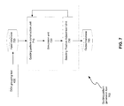
- FIG. 7 illustrates an example of a guiding pattern generation tool 700 that may be implemented according to various embodiments of the disclosed technology.
- the guiding pattern generation tool 700 includes a guiding pattern construction unit 710 , a simulation unit 720 , and a seeding position adjustment unit 730 .
- the guiding pattern construction unit 710 constructs a guiding pattern for a via-type feature group
- the simulation unit 720 determines a potential energy function for the guiding pattern and computes simulated locations of the via-type features in the via-type feature group
- the seeding position adjustment unit 730 determines whether one or more termination conditions are met and if not, changes seeding positions based on differences between the simulated locations and the targeted locations.
- some implementations of the guiding pattern generation tool 700 may cooperate with (or incorporate) one or more of the DSA-compliant feature grouping tool 400 , an input database 705 and an output database 745 . While the input database 705 and the output database 745 are shown as separate units in FIG. 7 , a single data storage medium may be used to implement some or both of these databases.
- one or more of the guiding pattern construction unit 710 , the simulation unit 720 , and the seeding position adjustment unit 730 are implemented by one or more computing systems, such as the computing system illustrated in FIGS. 1 and 2 , executing programmable instructions.
- some other embodiments of the disclosed technology may be implemented by software-executable instructions, stored on a non-transitory computer-readable medium, for instructing a computing system to perform functions of one or more of the guiding pattern construction unit 710 , the simulation unit 720 , and the seeding position adjustment unit 730 .
- non-transitory computer-readable medium refers to computer-readable medium that are capable of storing data for future retrieval, and not for propagating electro-magnetic waves.
- the non-transitory computer-readable medium may be, for example, a magnetic storage device, an optical storage device, a “punched” surface type device, or a solid state storage device.
- guiding pattern generation tool 700 in FIG. 7 and the flow chart 800 illustrated in FIG. 8 . It should be appreciated, however, that alternate implementations of a guiding pattern generation tool may be used to perform the methods of guiding pattern generation illustrated by the flow chart 800 according to various embodiments of the disclosed technology. Likewise, the guiding pattern generation tool 700 may be employed to perform other methods of guiding pattern generation according to various embodiments of the disclosed technology.
- the guiding pattern construction unit 710 constructs a guiding pattern for a via-type feature group based on seeding positions.
- the via-type feature group comprises two or more via-type features in a layout design.
- the two or more via-type features may be grouped together based on at least distances between neighboring via-type features of the two or more via-type features.
- the via-type feature group may be derived according to the flow chart 500 .
- the via-type feature group is DSA-compliant, which may be determined based on, for example, distorted areas.
- the seeding positions are initially derived from targeted locations of the two or more via-type features.
- FIG. 9 illustrates an example of constructing a guiding pattern that may be implemented according to various embodiments of the disclosed technology. Centers of features 910 , 912 and 914 are targeted locations of three via-type features, which are used as the initial seeding positions of the guiding pattern in this example. In this case, shapes of these via-type features are derived by changing the squares 910 , 912 and 914 into octagons 920 , 922 and 924 , respectively. It should be appreciated that other shapes such as hexagons or targeted shapes if provided may also be used.
- the octagons should be the shape formed by one polymer (A) in the di-block copolymer while the guiding pattern represents the shape of the other polymer (B).
- This contour is the contour for the polymer A, i.e., representing the boundary between the two polymers A and B.
- an appropriate threshold T may first be found to deliver the area ratio:
- the derived contour B 940 can be used as the contour for the guiding pattern.
- FIG. 10 illustrates another example of constructing a guiding pattern that may be implemented according to various embodiments of the disclosed technology. Similar to the example in FIG. 9 , the shape of a via-type feature 1010 may be represented by an octagon 1020 . A biased value d is then calculated to achieve desired area ratio. Based on the biased value d, a contour 1030 for the guiding pattern is constructed.
- the simulation unit 720 determines a potential energy function for the constructed guiding pattern.
- the potential energy function is at least a two-dimensional function and comprises a first portion representing interactions between via-type features in the via-type feature group and a second portion representing wall effects of the guiding pattern.
- the first portion may be expressed as:
- k>0 is a dimensionless Hooke coefficients. This formula neglects triple-, quadruple-, and other high order interactions between cells (via-type features).
- P is dimensionless
- E internal measures in units of area.
- ⁇ square root over (( x i ⁇ x j ) 2 +( y i ⁇ y j ) 2 ) ⁇ square root over (( x i ⁇ x j ) 2 +( y i ⁇ y j ) 2 ) ⁇ (5)
- r q >0 (7)
- the potential energy may also be assume as being always positive and with a fixed constant: P ( r ) ⁇ 0 (8) P ( r )
- Lennard-Jones potential There are many potentials (mainly coming from the physics of multi-body problems) that satisfy these requirements. First we mention Lennard-Jones potential:
- the Lennard-Jones potential may be very harsh in its repulsive part.
- the second portion of the potential energy function account for the effect of the walls of the guiding pattern. It may be represented by:
- S contour of the guiding pattern
- s i distance from the cell i to the element ds of the contour:
- s i ( s )
- Eq. (15) is illustrated by FIG. 11 . Note that Eq. (16) is normalized by q to be compatible with dimension of the internal energy E internal .
- the simulation unit 720 computes simulated locations of the two or more via-type features based on the potential energy function.
- the potential energy function for the via-type feature group such as Eq. (18) achieves a minimum value while the via-type features are maintained within the guiding pattern G:
- integrals in the potential energy function may be calculated using standard numerical methods or in exact analytical manner.
- the minimization may be solved by the standard GVSP (gradient variable scale projection) method.
- GVSP gradient variable scale projection
- the seeding position adjustment unit 730 determines whether one of one or more termination conditions is met.
- One termination condition may be the simulated locations match the targeted locations.
- a criterion for checking whether a simulated location matches the corresponding targeted location may be whether the distance between them is within a threshold value.
- Another termination condition may be whether the number of iterations reaches a predetermined number.
- the guiding pattern generation tool 700 may the generated guiding pattern in the output database 745 for further processes.
- the guiding pattern may be processed, for example, by OPC (optical proximity correction) and/or other resolution enhancement techniques. Then masks may then be produced using the circuit design that contains the guiding pattern.
- the seeding position adjustment unit 730 changes seeding positions based on differences between the simulated locations and the targeted locations. For each pair of simulated/targeted locations, a vector representing the location difference may be derived. The vector includes the distance value and the direction. The corresponding seeding position can then be adjusted based on the vector. Using the adjusted seeding position, the operations 810 - 850 are repeated. The seeding position adjustment is made so that the new guiding pattern will lead to the simulated locations closer to the targeted locations.
Landscapes
- Engineering & Computer Science (AREA)
- Physics & Mathematics (AREA)
- Theoretical Computer Science (AREA)
- Computer Hardware Design (AREA)
- General Physics & Mathematics (AREA)
- Evolutionary Computation (AREA)
- Geometry (AREA)
- General Engineering & Computer Science (AREA)
- Architecture (AREA)
- Design And Manufacture Of Integrated Circuits (AREA)
Abstract
Description
A:D(x,y)=0 (1)
This contour is the contour for the polymer A, i.e., representing the boundary between the two polymers A and B. The polymer B is assumed to fill space around the polymer A such that the area ratio B/A=B/A=(1−f)/f. To compute the contour for the polymer B, an appropriate threshold T may first be found to deliver the area ratio:
The contour for B may then be expressed as:
B:D(x,y)=T(f) (3)
The derived
where k>0 is a dimensionless Hooke coefficients. This formula neglects triple-, quadruple-, and other high order interactions between cells (via-type features). P is dimensionless, Einternal is measures in units of area. ri,j is pair-wise distances between centers of cells:
r i,j =|r 1 −r j|=√{square root over ((x i −x j)2+(y i −y j)2)}{square root over ((x i −x j)2+(y i −y j)2)} (5)
P′(r)|r=q=0 (6)
P″(r)|r=q>0 (7)
P(r)≧0 (8)
P(r)|r=q=0 (9)
And the potential may also be assumed to level off asymptotically for large distance so that
P(r→∞)→1 (10)
P(r)=[1−e −a(r-q)]2 (12)
Unlike the Lennard-Jones potential, this one can be adjusted by choosing parameter a that defines width of the well.
P(r)=P 4(ρ)=P 0 +c 1 ρ+c 2ρ2 +c 3ρ3 +c 4ρ4 (13)
where
To find coefficients cj, we set forth the following conditions:
P 4(0)=P 0 ; P 4(1)=0; P 4′(1)=0; P 4(2)=1; and P 4′(2)=0
where S is contour of the guiding pattern; si is distance from the cell i to the element ds of the contour:
s i(s)=|r i −r(s)| (15)
Here the contour is parameterized as
r=r(s) (16)
Eq. (15) is illustrated by
P wall(s i)=P 4(2ρi),ρi =s i /q (17)
Claims (20)
Priority Applications (1)
| Application Number | Priority Date | Filing Date | Title |
|---|---|---|---|
| US14/693,304 US9330228B2 (en) | 2013-11-18 | 2015-04-22 | Generating guiding patterns for directed self-assembly |
Applications Claiming Priority (2)
| Application Number | Priority Date | Filing Date | Title |
|---|---|---|---|
| US14/083,050 US9032357B1 (en) | 2013-11-18 | 2013-11-18 | Generating guiding patterns for directed self-assembly |
| US14/693,304 US9330228B2 (en) | 2013-11-18 | 2015-04-22 | Generating guiding patterns for directed self-assembly |
Related Parent Applications (1)
| Application Number | Title | Priority Date | Filing Date |
|---|---|---|---|
| US14/083,050 Continuation-In-Part US9032357B1 (en) | 2013-11-18 | 2013-11-18 | Generating guiding patterns for directed self-assembly |
Publications (2)
| Publication Number | Publication Date |
|---|---|
| US20150227676A1 US20150227676A1 (en) | 2015-08-13 |
| US9330228B2 true US9330228B2 (en) | 2016-05-03 |
Family
ID=53775144
Family Applications (1)
| Application Number | Title | Priority Date | Filing Date |
|---|---|---|---|
| US14/693,304 Active US9330228B2 (en) | 2013-11-18 | 2015-04-22 | Generating guiding patterns for directed self-assembly |
Country Status (1)
| Country | Link |
|---|---|
| US (1) | US9330228B2 (en) |
Cited By (3)
| Publication number | Priority date | Publication date | Assignee | Title |
|---|---|---|---|---|
| US20160292348A1 (en) * | 2015-03-30 | 2016-10-06 | Mentor Graphics Corporation | Optical Proximity Correction For Directed-Self-Assembly Guiding Patterns |
| US10586013B2 (en) * | 2018-01-30 | 2020-03-10 | International Business Machines Corporation | Calibration of directed self-assembly models using programmed defects of varying topology |
| US11329001B2 (en) | 2019-05-15 | 2022-05-10 | International Business Machines Corporation | Embedded chip identification formed by directed self-assembly |
Families Citing this family (6)
| Publication number | Priority date | Publication date | Assignee | Title |
|---|---|---|---|---|
| US9852260B2 (en) * | 2016-05-27 | 2017-12-26 | International Business Machines Corporation | Method and recording medium of reducing chemoepitaxy directed self-assembled defects |
| US10418245B2 (en) * | 2017-07-31 | 2019-09-17 | Taiwan Semiconductor Manufacturing Co., Ltd. | Method for integrated circuit manufacturing with directed self-assembly (DSA) |
| JP6875234B2 (en) * | 2017-09-13 | 2021-05-19 | キオクシア株式会社 | Guide layout creation device, creation method, and creation program |
| JP7246175B2 (en) * | 2018-12-12 | 2023-03-27 | 株式会社Preferred Networks | Estimation device, training device, estimation method and training method |
| CN111027272B (en) * | 2019-11-28 | 2024-12-31 | 中国科学院微电子研究所 | Method and device for generating through hole layer layout |
| CN113126575B (en) * | 2019-12-31 | 2022-07-26 | 捷普电子(无锡)有限公司 | Guiding method and guiding system for assembly operation process |
Citations (8)
| Publication number | Priority date | Publication date | Assignee | Title |
|---|---|---|---|---|
| US20110209106A1 (en) * | 2010-02-19 | 2011-08-25 | International Business Machines Corporation | Method for designing optical lithography masks for directed self-assembly |
| US8667430B1 (en) * | 2012-10-24 | 2014-03-04 | GlobalFoundries, Inc. | Methods for directed self-assembly process/proximity correction |
| US20140282344A1 (en) * | 2013-03-15 | 2014-09-18 | Taiwan Semiconductor Manufacturing Co., Ltd. | Layout boundary method |
| US20140282306A1 (en) * | 2013-03-15 | 2014-09-18 | Taiwan Semiconductor Manufacturing Company, Ltd. | Layout Optimization for Integrated Design |
| US20150012896A1 (en) * | 2013-07-08 | 2015-01-08 | GlobalFoundries, Inc. | Methods for fabricating integrated circuits including generating photomasks for directed self-assembly |
| US20150012897A1 (en) * | 2013-07-08 | 2015-01-08 | GLOBALFOUNDERIES, Inc. | Methods for fabricating integrated circuits including generating photomasks for directed self-assembly |
| US20150100287A1 (en) * | 2012-04-05 | 2015-04-09 | Commissariat A L'energie Atomique Et Aux Ene Alt | Method for simulating the self-assembly of block copolymers in order to design a printed circuit, corresponding design method, design system and computer program |
| US20150143313A1 (en) * | 2013-11-18 | 2015-05-21 | Mentor Graphics Corporation | Grouping Layout Features For Directed Self Assembly |
-
2015
- 2015-04-22 US US14/693,304 patent/US9330228B2/en active Active
Patent Citations (8)
| Publication number | Priority date | Publication date | Assignee | Title |
|---|---|---|---|---|
| US20110209106A1 (en) * | 2010-02-19 | 2011-08-25 | International Business Machines Corporation | Method for designing optical lithography masks for directed self-assembly |
| US20150100287A1 (en) * | 2012-04-05 | 2015-04-09 | Commissariat A L'energie Atomique Et Aux Ene Alt | Method for simulating the self-assembly of block copolymers in order to design a printed circuit, corresponding design method, design system and computer program |
| US8667430B1 (en) * | 2012-10-24 | 2014-03-04 | GlobalFoundries, Inc. | Methods for directed self-assembly process/proximity correction |
| US20140282344A1 (en) * | 2013-03-15 | 2014-09-18 | Taiwan Semiconductor Manufacturing Co., Ltd. | Layout boundary method |
| US20140282306A1 (en) * | 2013-03-15 | 2014-09-18 | Taiwan Semiconductor Manufacturing Company, Ltd. | Layout Optimization for Integrated Design |
| US20150012896A1 (en) * | 2013-07-08 | 2015-01-08 | GlobalFoundries, Inc. | Methods for fabricating integrated circuits including generating photomasks for directed self-assembly |
| US20150012897A1 (en) * | 2013-07-08 | 2015-01-08 | GLOBALFOUNDERIES, Inc. | Methods for fabricating integrated circuits including generating photomasks for directed self-assembly |
| US20150143313A1 (en) * | 2013-11-18 | 2015-05-21 | Mentor Graphics Corporation | Grouping Layout Features For Directed Self Assembly |
Non-Patent Citations (6)
| Title |
|---|
| Azat Latypov Computational solution of inverse directed self-assembly problem Alternative Lithographic Technologies V, edited by William M. Tong, Douglas J. Resnick, Proc. of SPIE vol. 8680, 2013 SPIE. |
| Azat Latypov, Moshe Preilb, Gerard Schmidc, Ji Xuc, He Yia , Kenji Yoshimotoc,d, Yi Zoua Exploration of the directed self-assembly based nano-fabrication design space using computational simulations Alternative Lithographic Technologies V, edited by William M. Tong, Douglas J. Resnick, Proc. of SPIE vol. 8680, 2013 SPIE. |
| Chi-Chun Liu. et al. "Progress towards the integration of optical proximity correction and directed self-assembly of block copolymers with graphoepitaxy" Alternative Lithographic Technologies IV, edited by William M. Tong, Douglas J. Resnick, Proc. of SPIE, vol. 8323, 2012. |
| F.M. Schellenberg, J.A.R. Torres Using Phase Mask Algorithms to Direct Self Assembly Proc. of SPIE vol. 6151, 13 pages. |
| Kafai Lai, et. al, Computational Aspects of Optical Lithography Extension by Directed Self-Assembly Optical Microlithography XXVI, edited by Will Conley, Proc. of SPIE vol. 8683. |
| William Hinsberg, Joy Cheng, Ho-Cheol Kim and Daniel P. Sanders Self-Assembling Materials for Lithographic Patterning: Overview, Status and Moving Forward Alternative Lithographic Technologies II, edited by Daniel J. C. Herr, Proc. of SPIE vol. 7637, 2010 SPIE. |
Cited By (4)
| Publication number | Priority date | Publication date | Assignee | Title |
|---|---|---|---|---|
| US20160292348A1 (en) * | 2015-03-30 | 2016-10-06 | Mentor Graphics Corporation | Optical Proximity Correction For Directed-Self-Assembly Guiding Patterns |
| US9836556B2 (en) * | 2015-03-30 | 2017-12-05 | Mentor Graphics Corporation | Optical proximity correction for directed-self-assembly guiding patterns |
| US10586013B2 (en) * | 2018-01-30 | 2020-03-10 | International Business Machines Corporation | Calibration of directed self-assembly models using programmed defects of varying topology |
| US11329001B2 (en) | 2019-05-15 | 2022-05-10 | International Business Machines Corporation | Embedded chip identification formed by directed self-assembly |
Also Published As
| Publication number | Publication date |
|---|---|
| US20150227676A1 (en) | 2015-08-13 |
Similar Documents
| Publication | Publication Date | Title |
|---|---|---|
| US9330228B2 (en) | Generating guiding patterns for directed self-assembly | |
| US10311165B2 (en) | Guiding patterns optimization for directed self-assembly | |
| JP5960953B2 (en) | A system for generating a single process window model | |
| US9652581B2 (en) | Directed self-assembly-aware layout decomposition for multiple patterning | |
| CN116710843B (en) | Optical proximity correction for freeform shapes | |
| US8713488B2 (en) | Layout design defect repair based on inverse lithography and traditional optical proximity correction | |
| US10691869B2 (en) | Pattern-based optical proximity correction | |
| US9111067B2 (en) | Grouping layout features for directed self assembly | |
| US10732499B2 (en) | Method and system for cross-tile OPC consistency | |
| US8788982B2 (en) | Layout design defect repair using inverse lithography | |
| US8826196B2 (en) | Integration of optical proximity correction and mask data preparation | |
| TW200532398A (en) | Design pattern correction method, mask producing method , semiconductor device producing method, mask pattern producing method, design pattern correction system and recording media | |
| KR102009552B1 (en) | Method for calculating the metrics of an ic manufacturing process | |
| US20120047473A1 (en) | Layout Decomposition Based on Partial Intensity Distribution | |
| US10418245B2 (en) | Method for integrated circuit manufacturing with directed self-assembly (DSA) | |
| US8191017B2 (en) | Site selective optical proximity correction | |
| US8683394B2 (en) | Pattern matching optical proximity correction | |
| US7974819B2 (en) | Methods and systems for intensity modeling including polarization | |
| TWI620007B (en) | Method and system for transferring patterns | |
| US9032357B1 (en) | Generating guiding patterns for directed self-assembly | |
| US9459523B2 (en) | Pattern optical similarity determination | |
| US8930856B2 (en) | Mask rule checking based on curvature | |
| JP4345804B2 (en) | Mask pattern correction program and mask pattern correction system | |
| US8799832B1 (en) | Optical proximity correction for topographically non-uniform substrates | |
| JP2008235553A (en) | Pattern creation method, pattern verification method, and program |
Legal Events
| Date | Code | Title | Description |
|---|---|---|---|
| AS | Assignment |
Owner name: MENTOR GRAPHICS CORPORATION, OREGON Free format text: ASSIGNMENT OF ASSIGNORS INTEREST;ASSIGNORS:ROBLES, JUAN ANDRES TORRES;MITRA, JOYDEEP;MA, YUANSHENG;AND OTHERS;SIGNING DATES FROM 20150420 TO 20150421;REEL/FRAME:035472/0834 |
|
| STCF | Information on status: patent grant |
Free format text: PATENTED CASE |
|
| MAFP | Maintenance fee payment |
Free format text: PAYMENT OF MAINTENANCE FEE, 4TH YEAR, LARGE ENTITY (ORIGINAL EVENT CODE: M1551); ENTITY STATUS OF PATENT OWNER: LARGE ENTITY Year of fee payment: 4 |
|
| AS | Assignment |
Owner name: SIEMENS INDUSTRY SOFTWARE INC., TEXAS Free format text: MERGER AND CHANGE OF NAME;ASSIGNORS:MENTOR GRAPHICS CORPORATION;SIEMENS INDUSTRY SOFTWARE INC.;REEL/FRAME:056675/0285 Effective date: 20201230 |
|
| MAFP | Maintenance fee payment |
Free format text: PAYMENT OF MAINTENANCE FEE, 8TH YEAR, LARGE ENTITY (ORIGINAL EVENT CODE: M1552); ENTITY STATUS OF PATENT OWNER: LARGE ENTITY Year of fee payment: 8 |